JP3958899B2 - Semiconductor memory device and manufacturing method thereof - Google Patents
Semiconductor memory device and manufacturing method thereof Download PDFInfo
- Publication number
- JP3958899B2 JP3958899B2 JP25078099A JP25078099A JP3958899B2 JP 3958899 B2 JP3958899 B2 JP 3958899B2 JP 25078099 A JP25078099 A JP 25078099A JP 25078099 A JP25078099 A JP 25078099A JP 3958899 B2 JP3958899 B2 JP 3958899B2
- Authority
- JP
- Japan
- Prior art keywords
- insulating film
- film
- semiconductor substrate
- forming
- silicon nitride
- Prior art date
- Legal status (The legal status is an assumption and is not a legal conclusion. Google has not performed a legal analysis and makes no representation as to the accuracy of the status listed.)
- Expired - Fee Related
Links
- 239000004065 semiconductor Substances 0.000 title claims description 161
- 238000004519 manufacturing process Methods 0.000 title claims description 27
- 239000000758 substrate Substances 0.000 claims description 101
- 239000012535 impurity Substances 0.000 claims description 76
- 238000009792 diffusion process Methods 0.000 claims description 71
- 238000000034 method Methods 0.000 claims description 18
- 239000000969 carrier Substances 0.000 claims description 12
- 239000002784 hot electron Substances 0.000 claims description 11
- 238000002955 isolation Methods 0.000 claims description 9
- 230000001590 oxidative effect Effects 0.000 claims description 4
- 238000000059 patterning Methods 0.000 claims description 4
- 229910052581 Si3N4 Inorganic materials 0.000 description 151
- HQVNEWCFYHHQES-UHFFFAOYSA-N silicon nitride Chemical compound N12[Si]34N5[Si]62N3[Si]51N64 HQVNEWCFYHHQES-UHFFFAOYSA-N 0.000 description 151
- VYPSYNLAJGMNEJ-UHFFFAOYSA-N Silicium dioxide Chemical compound O=[Si]=O VYPSYNLAJGMNEJ-UHFFFAOYSA-N 0.000 description 116
- 229910052814 silicon oxide Inorganic materials 0.000 description 116
- 239000010410 layer Substances 0.000 description 80
- XUIMIQQOPSSXEZ-UHFFFAOYSA-N Silicon Chemical compound [Si] XUIMIQQOPSSXEZ-UHFFFAOYSA-N 0.000 description 64
- 229910052710 silicon Inorganic materials 0.000 description 64
- 239000010703 silicon Substances 0.000 description 64
- 230000003647 oxidation Effects 0.000 description 32
- 238000007254 oxidation reaction Methods 0.000 description 32
- 230000015654 memory Effects 0.000 description 26
- 238000005468 ion implantation Methods 0.000 description 19
- 229910021420 polycrystalline silicon Inorganic materials 0.000 description 19
- 238000000206 photolithography Methods 0.000 description 16
- WQJQOUPTWCFRMM-UHFFFAOYSA-N tungsten disilicide Chemical compound [Si]#[W]#[Si] WQJQOUPTWCFRMM-UHFFFAOYSA-N 0.000 description 16
- 229910021342 tungsten silicide Inorganic materials 0.000 description 16
- NBIIXXVUZAFLBC-UHFFFAOYSA-N Phosphoric acid Chemical compound OP(O)(O)=O NBIIXXVUZAFLBC-UHFFFAOYSA-N 0.000 description 14
- 238000001312 dry etching Methods 0.000 description 14
- KRHYYFGTRYWZRS-UHFFFAOYSA-N Fluorane Chemical compound F KRHYYFGTRYWZRS-UHFFFAOYSA-N 0.000 description 12
- 238000005229 chemical vapour deposition Methods 0.000 description 11
- 238000002347 injection Methods 0.000 description 11
- 239000007924 injection Substances 0.000 description 11
- 239000011229 interlayer Substances 0.000 description 11
- QGZKDVFQNNGYKY-UHFFFAOYSA-N Ammonia Chemical compound N QGZKDVFQNNGYKY-UHFFFAOYSA-N 0.000 description 10
- 229910052782 aluminium Inorganic materials 0.000 description 10
- XAGFODPZIPBFFR-UHFFFAOYSA-N aluminium Chemical compound [Al] XAGFODPZIPBFFR-UHFFFAOYSA-N 0.000 description 10
- IJGRMHOSHXDMSA-UHFFFAOYSA-N Atomic nitrogen Chemical compound N#N IJGRMHOSHXDMSA-UHFFFAOYSA-N 0.000 description 9
- 150000002500 ions Chemical class 0.000 description 8
- 229910000147 aluminium phosphate Inorganic materials 0.000 description 7
- 229910052785 arsenic Inorganic materials 0.000 description 7
- RQNWIZPPADIBDY-UHFFFAOYSA-N arsenic atom Chemical compound [As] RQNWIZPPADIBDY-UHFFFAOYSA-N 0.000 description 7
- 238000005530 etching Methods 0.000 description 7
- 239000000243 solution Substances 0.000 description 7
- 230000001133 acceleration Effects 0.000 description 6
- 238000000137 annealing Methods 0.000 description 6
- OAICVXFJPJFONN-UHFFFAOYSA-N Phosphorus Chemical compound [P] OAICVXFJPJFONN-UHFFFAOYSA-N 0.000 description 5
- 230000015572 biosynthetic process Effects 0.000 description 5
- 229910052698 phosphorus Inorganic materials 0.000 description 5
- 239000011574 phosphorus Substances 0.000 description 5
- 229910021529 ammonia Inorganic materials 0.000 description 4
- 238000006243 chemical reaction Methods 0.000 description 4
- QPJSUIGXIBEQAC-UHFFFAOYSA-N n-(2,4-dichloro-5-propan-2-yloxyphenyl)acetamide Chemical compound CC(C)OC1=CC(NC(C)=O)=C(Cl)C=C1Cl QPJSUIGXIBEQAC-UHFFFAOYSA-N 0.000 description 4
- 230000005684 electric field Effects 0.000 description 3
- 230000006870 function Effects 0.000 description 3
- 239000007789 gas Substances 0.000 description 3
- 238000007654 immersion Methods 0.000 description 3
- 229910052757 nitrogen Inorganic materials 0.000 description 3
- 230000002093 peripheral effect Effects 0.000 description 3
- 230000008569 process Effects 0.000 description 3
- 230000001681 protective effect Effects 0.000 description 3
- 238000004544 sputter deposition Methods 0.000 description 3
- 238000001039 wet etching Methods 0.000 description 3
- ZOXJGFHDIHLPTG-UHFFFAOYSA-N Boron Chemical compound [B] ZOXJGFHDIHLPTG-UHFFFAOYSA-N 0.000 description 2
- 230000009471 action Effects 0.000 description 2
- 229910052796 boron Inorganic materials 0.000 description 2
- 230000015556 catabolic process Effects 0.000 description 2
- 238000010586 diagram Methods 0.000 description 2
- 229910021332 silicide Inorganic materials 0.000 description 2
- FVBUAEGBCNSCDD-UHFFFAOYSA-N silicide(4-) Chemical compound [Si-4] FVBUAEGBCNSCDD-UHFFFAOYSA-N 0.000 description 2
- WFKWXMTUELFFGS-UHFFFAOYSA-N tungsten Chemical compound [W] WFKWXMTUELFFGS-UHFFFAOYSA-N 0.000 description 2
- 229910052721 tungsten Inorganic materials 0.000 description 2
- 239000010937 tungsten Substances 0.000 description 2
- 230000004913 activation Effects 0.000 description 1
- 229910021419 crystalline silicon Inorganic materials 0.000 description 1
- 230000007423 decrease Effects 0.000 description 1
- 230000007547 defect Effects 0.000 description 1
- 238000006731 degradation reaction Methods 0.000 description 1
- 230000003111 delayed effect Effects 0.000 description 1
- 238000009826 distribution Methods 0.000 description 1
- 230000000694 effects Effects 0.000 description 1
- 238000010893 electron trap Methods 0.000 description 1
- 238000010438 heat treatment Methods 0.000 description 1
- 230000007246 mechanism Effects 0.000 description 1
- 229910052751 metal Inorganic materials 0.000 description 1
- 239000002184 metal Substances 0.000 description 1
- 238000005498 polishing Methods 0.000 description 1
- 239000000126 substance Substances 0.000 description 1
Images


Classifications
-
- H—ELECTRICITY
- H01—ELECTRIC ELEMENTS
- H01L—SEMICONDUCTOR DEVICES NOT COVERED BY CLASS H10
- H01L29/00—Semiconductor devices adapted for rectifying, amplifying, oscillating or switching, or capacitors or resistors with at least one potential-jump barrier or surface barrier, e.g. PN junction depletion layer or carrier concentration layer; Details of semiconductor bodies or of electrodes thereof ; Multistep manufacturing processes therefor
- H01L29/66—Types of semiconductor device ; Multistep manufacturing processes therefor
- H01L29/68—Types of semiconductor device ; Multistep manufacturing processes therefor controllable by only the electric current supplied, or only the electric potential applied, to an electrode which does not carry the current to be rectified, amplified or switched
- H01L29/76—Unipolar devices, e.g. field effect transistors
- H01L29/772—Field effect transistors
- H01L29/78—Field effect transistors with field effect produced by an insulated gate
- H01L29/788—Field effect transistors with field effect produced by an insulated gate with floating gate
-
- H—ELECTRICITY
- H01—ELECTRIC ELEMENTS
- H01L—SEMICONDUCTOR DEVICES NOT COVERED BY CLASS H10
- H01L29/00—Semiconductor devices adapted for rectifying, amplifying, oscillating or switching, or capacitors or resistors with at least one potential-jump barrier or surface barrier, e.g. PN junction depletion layer or carrier concentration layer; Details of semiconductor bodies or of electrodes thereof ; Multistep manufacturing processes therefor
- H01L29/66—Types of semiconductor device ; Multistep manufacturing processes therefor
- H01L29/68—Types of semiconductor device ; Multistep manufacturing processes therefor controllable by only the electric current supplied, or only the electric potential applied, to an electrode which does not carry the current to be rectified, amplified or switched
- H01L29/76—Unipolar devices, e.g. field effect transistors
- H01L29/772—Field effect transistors
- H01L29/78—Field effect transistors with field effect produced by an insulated gate
- H01L29/792—Field effect transistors with field effect produced by an insulated gate with charge trapping gate insulator, e.g. MNOS-memory transistors
- H01L29/7923—Programmable transistors with more than two possible different levels of programmation
-
- H—ELECTRICITY
- H01—ELECTRIC ELEMENTS
- H01L—SEMICONDUCTOR DEVICES NOT COVERED BY CLASS H10
- H01L29/00—Semiconductor devices adapted for rectifying, amplifying, oscillating or switching, or capacitors or resistors with at least one potential-jump barrier or surface barrier, e.g. PN junction depletion layer or carrier concentration layer; Details of semiconductor bodies or of electrodes thereof ; Multistep manufacturing processes therefor
- H01L29/40—Electrodes ; Multistep manufacturing processes therefor
- H01L29/401—Multistep manufacturing processes
- H01L29/4011—Multistep manufacturing processes for data storage electrodes
- H01L29/40117—Multistep manufacturing processes for data storage electrodes the electrodes comprising a charge-trapping insulator
-
- H—ELECTRICITY
- H01—ELECTRIC ELEMENTS
- H01L—SEMICONDUCTOR DEVICES NOT COVERED BY CLASS H10
- H01L29/00—Semiconductor devices adapted for rectifying, amplifying, oscillating or switching, or capacitors or resistors with at least one potential-jump barrier or surface barrier, e.g. PN junction depletion layer or carrier concentration layer; Details of semiconductor bodies or of electrodes thereof ; Multistep manufacturing processes therefor
- H01L29/66—Types of semiconductor device ; Multistep manufacturing processes therefor
- H01L29/68—Types of semiconductor device ; Multistep manufacturing processes therefor controllable by only the electric current supplied, or only the electric potential applied, to an electrode which does not carry the current to be rectified, amplified or switched
- H01L29/76—Unipolar devices, e.g. field effect transistors
- H01L29/772—Field effect transistors
- H01L29/78—Field effect transistors with field effect produced by an insulated gate
- H01L29/792—Field effect transistors with field effect produced by an insulated gate with charge trapping gate insulator, e.g. MNOS-memory transistors
-
- H—ELECTRICITY
- H10—SEMICONDUCTOR DEVICES; ELECTRIC SOLID-STATE DEVICES NOT OTHERWISE PROVIDED FOR
- H10B—ELECTRONIC MEMORY DEVICES
- H10B43/00—EEPROM devices comprising charge-trapping gate insulators
- H10B43/30—EEPROM devices comprising charge-trapping gate insulators characterised by the memory core region
Description
【0001】
【発明の属する技術分野】
本発明は、半導体記憶装置及びその製造方法に関し、特に、1つのメモリセルに2ビットの情報を記録可能な不揮発性半導体メモリに用いて好適なものである。
【0002】
【従来の技術】
近年、キャリアの注入位置を異ならせることにより、1つのメモリセルに2ビットの情報を記録可能とした不揮発性半導体メモリが研究、開発されている。この不揮発性半導体メモリは、ゲートの下層に設けられた電荷捕獲膜にキャリアを捕獲するメモリであって、情報を書き込む場合と読み出す場合とでソース/ドレイン間に印加する電圧の方向を逆方向とし、チャネル領域の両端部に相当する位置における電荷捕獲膜中にそれぞれ独立して電子を捕獲するように構成されている。そして、両端部それぞれにおける電子の捕獲の有無によって2ビットの情報を記録可能としている。
【0003】
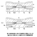
例えば、国際公開WO 99/07000号公報には、上述した構成の不揮発性半導体メモリが開示されている。図8を参照しながら、同公報に開示された不揮発性半導体メモリの構成及びデータの書き込み/読み出しの動作について簡単に説明する。
【0004】
図8に示すように、不揮発性半導体メモリ100は、p型シリコン半導体基板101の表面領域に形成されたソース/ドレインとして機能する1対の不純物拡散層102,103と、当該不純物拡散層102,103間のp型シリコン半導体基板101上に形成された3層構造の絶縁膜及び当該3層構造の絶縁膜上に形成されたゲート電極107から成る。ここで、3層構造の絶縁膜はゲート絶縁膜(シリコン酸化膜)104、電荷捕獲膜(シリコン窒化膜)105、シリコン酸化膜106から構成されている。
【0005】
この不揮発性半導体メモリ100においては、電荷捕獲膜中のチャネル領域の両端部に相当する位置にそれぞれ独立して電子を捕獲するように構成され、RIGHT BIT及びLEFT BITのそれぞれに1ビット、合計2ビットの情報を記録することが可能とされている。情報の記録は、ゲート絶縁膜104と電荷捕獲膜105の界面に電子が注入されることによって成され、RIGHT BITに情報を記録する場合には、図8に示す領域109に電子が注入され、LEFT BITに情報を記録する場合には、領域108に電子が注入される。
【0006】
RIGHT BITへ情報を書き込む場合には、例えばソースを0V、ドレインを5V程度としてソース/ドレイン間に電位差を生じさせ、ゲート107に高電圧(10V程度)を印加してソース/ドレイン間にチャネル110を形成する。ここで、形成されたチャネル110の範囲l1 は同電位であり電界は生じない。チャネル110が形成されていない範囲l2 ではソース/ドレイン間の電位差に起因して電界が生じるため、この範囲l2 においてチャネルホットエレクトロンが発生し、領域109に電子が捕獲(トラップ)される。
【0007】
RIGHT BITから情報を読み出す場合には、書き込みの場合と逆方向の電圧をソース/ドレイン間に印加する。この際、領域109に電子が捕獲されているため、領域109の下層で不純物拡散層103から不純物拡散層102に向かってチャネルが形成されず、しきい値が上昇しているためソース/ドレイン間には電流が流れない。領域109に電子を捕獲していない場合にはソース/ドレイン間にチャネルが形成されて電流が流れるため、電子の捕獲の有無に対応して1ビットの情報を記憶することが可能である。
【0008】
領域109に電子を捕獲した場合において、読み出しの際に書き込みと同じ方向に電圧を印加すると、ソース/ドレイン間にチャネルが形成されて電流が流れてしまうため、情報を読み出す場合には、上述したように書き込みの場合と逆方向の電圧をソース/ドレイン間に印加する必要がある。
【0009】
LEFT BITへの情報の書き込み、読み出しもRIGHT BITの場合と同様に行うことができ、RIGHT BITへの情報の書き込み、読み出しの際に印加する電圧の方向に対してそれぞれ逆方向の電圧を印加することによって行うことができる。
【0010】
【発明が解決しようとする課題】
しかしながら、例えばRIGHT BITに情報を書き込む場合において、書き込み時にメモリセルのしきい値を上昇させるために発生させたチャネルホットエレクトロンの注入位置は、ドレイン103とゲート電極107に印加する電圧に応じて変動するため、上述した従来の構成では、領域109に電子を局在させる必要があるにもかかわらず、本来電子が注入されるべきではないチャネル中央部のゲート絶縁膜104中にも電子が捕獲されるという問題が生じる。
【0011】
また、しきい値が上昇した状態(例えば書き込み状態)において、メモリセルのしきい値を下降させる(例えば消去動作)際に注入されるホットホールは、上述のホットエレクトロンとは発生メカニズムが異なるため、両者の注入位置は必ずしも一致しない。このため、書き込み、消去を繰り返すうちに、いずれか一方の電荷がシリコン窒化膜105中に残る場合が生じ、書き込み又は消去不良が起こるという問題があった。
【0012】
この問題は、しきい値を上昇させる場合には電子を過剰に注入し、しきい値を下降させる場合にはホールを過剰に注入することにより軽減することができるものの、キャリアを過剰に注入すると、書き込み、消去速度の遅延が起こり、素子の性能を劣化させてしまうという別の問題が生じてしまう。また、キャリアの過剰な注入は必要以上の電気的ストレスを絶縁膜に印加することになるため、経時絶縁破壊等の原因となり素子の信頼性の観点からも望ましくない。
【0013】
また、ホール注入の際の電圧印加条件を電子の注入位置の分布に合わせる方法を選択すると、ホールの発生効率は必ずしも最適とはならないため、やはり素子特性の劣化を招来することとなる。
【0014】
本発明は、このような問題を解決するために成されたものであり、キャリアの注入位置を異ならせて2ビットの情報を記録する半導体記憶装置において、2ビットの情報を確実に記録、保持することを可能とし、書き込み不良又は消去不良の発生を抑止して信頼性を向上させた半導体記憶装置及びその製造方法を提供することを目的とする。
【0015】
【課題を解決するための手段】
本発明の半導体記憶装置は、半導体基板の表面領域に形成された1対の不純物拡散層と、前記1対の不純物拡散層間における前記半導体基板上にゲート絶縁膜を介して形成されたゲート電極とを備え、前記ゲート電極に所定電圧を印加することにより前記ゲート絶縁膜にキャリアを捕獲するように成された半導体記憶装置であって、前記1対の不純物拡散層のそれぞれに近接する位置における前記ゲート絶縁膜中に、前記ゲート絶縁膜に比してキャリアトラップ特性が高い電荷捕獲膜が形成されており、前記ゲート絶縁膜は、前記1対の不純物拡散層のそれぞれに近接する位置が他の領域に比して薄く形成されており、ホットエレクトロン又はホットホールからなるキャリアを前記1対の不純物拡散層に近接する位置に形成された2つの前記電荷捕獲膜にそれぞれ注入することによって2つのビットの情報を記憶する。
【0019】
本発明の半導体記憶装置の一態様例においては、前記ゲート絶縁膜上に別の電荷捕獲膜が形成され、前記ゲート絶縁膜上に当該別の電荷捕獲膜を介して前記ゲート電極が形成されている。
【0020】
本発明の半導体記憶装置の製造方法は、ホットエレクトロン又はホットホールからなるキャリアを一対の不純物拡散層に近接する位置に形成された2つの電荷捕獲膜にそれぞれ注入することによって2つのビットの情報を記憶する半導体装置の製造方法に関し、半導体基板上に第1及び第2の絶縁膜を順次形成する第1の工程と、前記第1及び第2の絶縁膜を選択的に除去して共にパターニングする第2の工程と、露出した前記半導体基板上から前記第2の絶縁膜の下方の所定範囲にかけての前記半導体基板上に第3の絶縁膜を形成する第3の工程と、前記第2の絶縁膜をマスクとして前記半導体基板に不純物を導入し、前記第2の絶縁膜の両側の前記半導体基板の表面領域に各々が独立した一対の不純物拡散層を形成する第4の工程と、前記第2の絶縁膜の下方の所定範囲に形成された前記第3の絶縁膜を残し、他の領域の前記第3の絶縁膜を除去して前記半導体基板を露出させる第5の工程と、露出した前記半導体基板を熱酸化して素子分離膜を形成する第6の工程と、前記第1及び第2の絶縁膜を除去して、下層の前記半導体基板及び前記第3の絶縁膜を露出させ、当該第3の絶縁膜を電荷捕獲膜とする第7の工程と、露出した前記半導体基板の表面を熱酸化して第4の絶縁膜を形成し、前記電荷捕獲膜の上層及び下層を当該第4の絶縁膜で覆う第8の工程と、前記第4の絶縁膜の上層に導電膜を形成する第9の工程と、前記導電膜をゲート電極形状にパターニングする第10の工程とを有する。
【0021】
本発明の半導体記憶装置の製造方法の一態様例においては、前記第2の工程と前記第3の工程の間に、前記第1の絶縁膜をパターン幅方向に所定量除去して、前記第2の絶縁膜のパターン幅よりも幅狭にする第11の工程を更に有し、前記第3の工程において、露出した前記半導体基板上及び前記所定量の範囲における前記半導体基板上に前記第3の絶縁膜を形成する。
【0022】
本発明の半導体記憶装置の製造方法の一態様例においては、前記第8の工程と前記第9の工程の間に、前記第4の絶縁膜上に第5の絶縁膜を形成する第12の工程を更に有し、前記第9の工程において前記第4の絶縁膜上に前記第5の絶縁膜を介して前記導電膜を形成する。
【0023】
本発明の半導体記憶装置の製造方法は、ホットエレクトロン又はホットホールからなるキャリアを一対の不純物拡散層に近接する位置に形成された2つの電荷捕獲膜にそれぞれ注入することによって2つのビットの情報を記憶する半導体装置の製造方法に関し、半導体基板上に第1の絶縁膜を形成する工程と、前記第1の絶縁膜を選択的に除去して下層の前記半導体基板を露出させる工程と、前記第1の絶縁膜をマスクとして露出した前記半導体基板に不純物を導入し、前記第1の絶縁膜の両側の前記半導体基板の表面領域に各々が独立した一対の不純物拡散層を形成する工程と、前記不純物拡散層上及び前記第1の絶縁膜を覆うように第2の絶縁膜を形成する工程と、前記第1の絶縁膜上の前記第2の絶縁膜を除去し、前記第1の絶縁膜を露出させる工程と、前記第1の絶縁膜を除去して下層の前記半導体基板を露出させ、この領域を素子活性領域とする工程と、前記素子活性領域における前記半導体基板上に第3の絶縁膜を形成する工程と、前記第3の絶縁膜上に第4の絶縁膜を形成する工程と、前記第4及び第2の絶縁膜を覆うように第5の絶縁膜を形成する工程と、前記素子活性領域の両側にのみ残存するように前記第5の絶縁膜を除去して、前記第2の絶縁膜の側壁に前記第5の絶縁膜から成るサイドウォールを形成するとともに、前記素子活性領域における前記半導体基板を露出させる工程と、露出した前記半導体基板上に第6の絶縁膜を形成する工程と、前記サイドウォールを除去して前記サイドウォールの下層の前記第4の絶縁膜を露出させ、当該第4の絶縁膜を電荷捕獲膜とする工程と、前記電荷捕獲膜上に第7の絶縁膜を形成する工程と、前記第6及び第7の絶縁膜上を覆う導電膜を形成する工程とを有する。
【0024】
【作用】
本発明は上記技術手段より成るので、データ書き込み時にゲート電極に高電圧を印加してホットエレクトロンを発生させると、ゲート絶縁膜中において、チャネル幅中央部よりもキャリアトラップ特性の高い端部に電子が注入されることとなる。これにより、ゲート電極下のゲート絶縁膜の端部に集中的に電子を捕獲することが可能となる。データ消去時にも同様に、ホットホールをゲート絶縁膜の端部に集中的に注入することができるため、安定してデータの消去が行われることとなる。
【0025】
【発明の実施の形態】
以下、本発明のいくつかの実施形態に係る不揮発性半導体メモリの構成及びその製造方法を、図面を参照しながら共に説明する。
【0026】
(第1の実施形態)
先ず、第1の実施形態について説明する。図1は第1の実施形態に係る不揮発性半導体メモリの製造方法を工程順に示す概略断面図である。また、図2及び図3は第1の実施形態に係る不揮発性半導体メモリの平面構成を示す概略平面図である。ここで、図1は不揮発性半導体メモリの1つのメモリセルに着目し、当該メモリセルの断面を製造工程順に示した図であって、図3の一点鎖線I−I’に沿った位置に対応する断面を示している。
【0027】
先ず、p型シリコン半導体基板1上に所定のウェルを形成し、更に周辺回路領域の素子分離を行う(不図示)。次に、図1(a)に示すように、メモリセルの領域において、熱酸化法によりシリコン酸化膜2を20nm程度の膜厚まで成長させ、シリコン酸化膜2上にCVD法によりシリコン窒化膜3を200nm程度の膜厚で堆積する。
【0028】
その後、フォトリソグラフィー及びこれに続くエッチングにより、メモリセルのチャネル領域となる部位のp型シリコン半導体基板1上にはシリコン窒化膜3及びシリコン酸化膜2を残し、その他の領域のシリコン窒化膜3及びシリコン酸化膜2を除去する。
【0029】
次に、図1(b)に示すように、アンモニア(NH3 )ガス雰囲気下において、温度950℃程度、時間20分から120分程度の条件にてアニール処理を行い、露出したp型シリコン半導体基板1上からシリコン窒化膜3のパターン端部の下層の所定範囲にかけてシリコン窒化膜4を形成する。この際に、表面に露出したp型シリコン半導体基板1においては、シリコンとアンモニアガスの直接反応によりシリコン窒化膜4が形成される。また、シリコン窒化膜3のパターン端部下においては、シリコン酸化膜2中を拡散したアンモニアとの反応でシリコン窒化膜4が形成される。シリコン窒化膜4の成膜条件を調整することにより、シリコン窒化膜3のパターン端に形成されるシリコン窒化膜4の幅を制御することができる。
【0030】
なお、シリコン窒化膜4の形成はイオン注入法によって行っても良い。この場合には、窒素(N2 )等を含むイオンを、加速エネルギー30keV程度、ドーズ量1×10¹⁶(ions/cm2 )程度の条件でイオン注入し、アニールすることによりp型シリコン半導体基板1の表面付近に窒素を含んだ膜を形成する。この際、p型シリコン半導体基板1に対するイオン注入の角度を制御することで、シリコン窒化膜3のパターン端の下層に形成されるシリコン窒化膜4の幅を制御することができる。
【0031】
次に、図1(c)に示すように、シリコン窒化膜3をマスクとしてp型シリコン半導体基板1の表面領域にイオン注入を行う。具体的には、n型の不純物である砒素(As)を加速エネルギー50keV程度、ドーズ量を1×10¹⁶(ions/cm2 )程度の条件でイオン注入する。このイオン注入により打ち込まれた不純物は、シリコン窒化膜3の両側のp型シリコン半導体基板1の表面領域における、ソース/ドレインとして機能する1対の不純物拡散層6となる。本実施形態において、不純物拡散層6はビットラインとして機能するため、図2に示すように、不純物拡散層6は複数本が所定方向に延在するように形成され各メモリセルと接続される。
【0032】
次に、図1(d)に示すように、シリコン窒化膜3をマスクとして、熱酸化によりp型シリコン半導体基板1の表面を選択酸化する。この際、図1(c)の工程におけるイオン注入によって、砒素が打ち込まれた領域のシリコン窒化膜4の耐酸化性は失われているため、図1(d)に示す工程での熱酸化によりシリコン窒化膜3の下層以外のp型シリコン半導体基板1の表面が酸化されて、いわゆるLOCOS(Local oxidation of silicon)素子分離としてのシリコン酸化膜5が成長する。そして、シリコン酸化膜5によってp型シリコン半導体基板1上に素子活性領域が画定される。
【0033】
次に、図1(e)に示すように、p型シリコン半導体基板1を温度150℃程度のリン酸溶液中に浸し、シリコン窒化膜3を溶解して除去する。この際、シリコン窒化膜3の下層に形成されているシリコン窒化膜4は、上面がシリコン酸化膜2で覆われて保護されているため、リン酸によって除去されることなくシリコン酸化膜2下に残存する。
【0034】
次に、図1(f)に示すように、p型シリコン半導体基板1上のシリコン酸化膜2をフッ酸(HF)溶液に浸して除去する。その後、熱酸化を施して、ゲート絶縁膜としてのシリコン酸化膜7を膜厚15nm程度形成する。この際、シリコン窒化膜4が形成されている部位では、シリコン窒化膜4の作用により熱酸化による酸化速度が低下するため、この位置におけるシリコン酸化膜7は他の領域に比して薄く形成される。この熱酸化によってシリコン窒化膜4はシリコン酸化膜7によって覆われ、1対の不純物拡散層6のそれぞれの近傍におけるp型シリコン半導体基板1上には、シリコン酸化膜7中にシリコン窒化膜4を含む構造のゲート絶縁膜が形成される。
【0035】
シリコン窒化膜4はシリコン酸化膜7に比してキャリアトラップ特性が高いため、ゲート絶縁膜として機能するシリコン酸化膜7中の一部にシリコン窒化膜4を含ませることによって、この部位におけるキャリアトラップ特性をシリコン酸化膜7の他の領域に比して向上させることができる。すなわち、シリコン酸化膜7の端部にシリコン窒化膜4を形成することによって、チャネル領域の中央近傍に比してチャネル領域端部の電気容量換算膜厚を小さくしたゲート絶縁膜を形成することができる。しかも、シリコン窒化膜4が形成されていない領域では、シリコン窒化膜4が形成された領域よりもシリコン酸化膜7が厚く形成されているため、上部に形成するゲート電極に電圧を印加した場合、ゲート酸化膜7へのキャリアトラップが抑制される。従って、チャネル領域の中央近傍に比してチャネル領域端部におけるキャリアトラップ特性を高めることができる。
【0036】
次に、図1(g)に示すように、CVD法によりリン(P)がドープされた多結晶シリコン膜8をp型シリコン半導体基板1上の全面に形成し、更に、CVD法により多結晶シリコン膜8上にタングステンシリサイド膜9を膜厚100nm程度堆積する。その後、フォトリソグラフィー及びこれに続くドライエッチングにより、多結晶シリコン膜8及びタングステンシリサイド膜9をゲート電極形状にパターニングする。これにより、多結晶シリコン膜8及びタングステンシリサイド膜9から成るポリサイド構造のゲート電極が形成される。そして、以上の工程により、トランジスタの主要部分であるソース/ドレイン拡散層(不純物拡散層6)、ゲート絶縁膜(シリコン酸化膜7、シリコン窒化膜4)、ゲート電極(多結晶シリコン膜8、タングステンシリサイド膜9)の形成が完了する。
【0037】
その後、一般的な配線層の形成工程を行い本実施形態に係る不揮発性半導体メモリを完成させる。すなわち、CVD法により層間絶縁膜(シリコン酸化膜等)を堆積して、多結晶シリコン膜8及びタングステンシリサイド膜9から成るゲート電極を覆い、フォトリソグラフィー及びこれに続くドライエッチングにより、層間絶縁膜にコンタクトホールを形成する。そして、層間絶縁膜上に配線層として例えばアルミニウム膜をスパッタ法により堆積してコンタクトホールを充填し、フォトリソグラフィー及びこれに続くドライエッチングにより、アルミニウム膜を所定形状にパターニングする。その後、アルミニウム膜を覆うように保護膜を形成する。
【0038】
図2は、完成した本実施形態に係る不揮発性半導体メモリの全体の平面構成を示す図であり、ゲート電極上の層間絶縁膜及びアルミニウム膜は図示を省略している。図2に示すように、ゲート電極(多結晶シリコン膜8、タングステンシリサイド膜9)は複数本が並んで配置され、やはり複数本並んで形成された不純物拡散層6に対して直交するように形成される。
【0039】
図3は、図2中の二点鎖線で囲まれた領域Aを拡大して示す模式図であり、素子分離膜としてのシリコン酸化膜5は図示を省略している。図3において、二点鎖線Bで囲まれた領域が1つのメモリセルを構成する領域である。図3に示すように、シリコン窒化膜4は不純物拡散層6の両側に沿って形成され、シリコン酸化膜7を介して対向するように配置されている。データの書き込み、消去は、選択されたメモリセルに対応するゲート電極を高電位とし、当該メモリセルの両側の不純物拡散層6間に電位差を与えることにより行うことができる。
【0040】
図4は、データの書き込み及び読み出しの動作を示す模式図である。データを書き込む際には、図4(a)に示すように、右側に位置する不純物拡散層6aをソースとして接地し、左側に位置する不純物拡散層6bをドレインとして5V程度の電圧を印加する。そして、ゲート電極に高電圧(10V)程度を印加することにより、ドレイン(不純物拡散層6b)近傍でホットエレクトロンが発生してシリコン窒化膜4bに電子eが捕獲される。この際、電子eを捕獲するシリコン窒化膜4bをドレイン近傍にのみ形成し、チャネル幅中央近傍に形成していないため、シリコン窒化膜4bが形成された領域にのみ電子eが捕獲されることになる。従って、シリコン窒化膜4bが形成された領域以外への電子eの捕獲を抑止して、データの書き込みの信頼性を向上させることができる。
【0041】
データを消去する際には、不純物拡散層6aを開放し、不純物拡散層6bをドレインとして5V程度の電圧を印加する。そして、ゲート電極に負電圧(−5V程度)を印加することにより、ドレイン(不純物拡散層6b)近傍でホットホールが発生してシリコン窒化膜4bにホールが捕獲される。この際、ホールを捕獲するシリコン窒化膜4bをドレイン近傍にのみ形成し、チャネル幅中央近傍に形成していないため、シリコン窒化膜4bが形成された領域にのみホールが捕獲されることになり、捕獲されている電子eを確実に消去することができる。従って、データの消去の信頼性を向上させることが可能となる。
【0042】
データを読み出す際には、図4(b)に示すように、不純物拡散層6bをソースとして接地し、不純物拡散層6aをドレインとして1.6V程度の電圧を印加する。シリコン窒化膜4bに電子eが捕獲されている場合には、捕獲された電子eにより生じる負電界によりチャネル消失するため,しきい値が上昇し、不純物拡散層6a,6b間には電流が流れない。シリコン窒化膜4bに電子eが捕獲されていない場合には、チャネルが消失せず、不純物拡散層6a,6b間に電流が流れる。従って、シリコン窒化膜4bへの電子eの捕獲の有無に対応して、1ビットの情報を記憶することが可能である。
【0043】
シリコン窒化膜4aへのデータを書き込み、読み出しは、上述したシリコン窒化膜4bへのデータを書き込み、読み出しと逆方向の電圧を印加することにより行うことができる。これにより、シリコン窒化膜4a,4bに2ビットの情報を記録することが可能となる。
【0044】
以上説明したように、本発明の第1の実施形態によれば、ゲート酸化膜7の両端にキャリアトラップ特性の高いシリコン窒化膜4を形成しているため、構造的に電荷の注入箇所が限定されることとなり、確実にシリコン窒化膜4の近傍のみにキャリアをトラップすることが可能となる。これにより、情報を記録する際に、ゲート電極(多結晶シリコン膜8、タングステンシリサイド膜9)を高電位とし、1対の不純物拡散層6間に電位差を与えた場合において、ゲート電極の電位や1対の不純物拡散層6間の電位差のバラツキ等に影響を受けることなく、確実にシリコン窒化膜4近傍に電子をトラップすることができ、他の領域に電子がトラップされることを抑止することができる。また、データの消去時においても、確実にシリコン窒化膜4近傍に正孔(ホール)をトラップすることができ、他の領域に正孔が捕獲されることを抑止することができる。これにより、必要最小限のキャリアの注入により、安定かつ確実にデータの記録及び消去を行うことが可能となる。
【0045】
(第2の実施形態)
次に、本発明の第2の実施形態について説明する。図5は第2の実施形態に係る不揮発性半導体メモリの製造方法を工程順に示す概略断面図である。第2の実施形態に係る不揮発性半導体メモリの平面構成は、図2及び図3に示した第1の実施形態に係る不揮発性半導体メモリの平面構成と同様である。ここで、図5は不揮発性半導体メモリの1つのメモリセルに着目し、当該メモリセルの断面を製造工程順に示した図であって、第1の実施形態と同様、図3の一点鎖線I−I’に沿った位置に対応する断面を示している。なお、図5において、第1の実施形態と共通の構成要素については図1と同様の符号を記して説明する。
【0046】
先ず、p型シリコン半導体基板1上に所定のウェルを形成し、更に周辺回路領域の素子分離を行う(不図示)。次に、図5(a)に示すように、メモリセルの領域において、熱酸化法によりシリコン酸化膜2を20nm程度の膜厚まで成長させ、シリコン酸化膜2上にCVD法によりシリコン窒化膜3を200nm程度の膜厚で堆積する。
【0047】
その後、フォトリソグラフィー及びこれに続くエッチングにより、メモリセルのチャネル領域となる部位のp型シリコン半導体基板1上にはシリコン窒化膜3及びシリコン酸化膜2を残し、その他の領域のシリコン窒化膜3及びシリコン酸化膜2を除去する。
【0048】
次に、図5(b)に示すように、p型シリコン半導体基板1をフッ酸(HF)溶液に浸し、シリコン酸化膜2を横幅方向に50nm程度ウエットエッチングする。このエッチングにより、シリコン酸化膜2の幅がシリコン窒化膜3の幅よりも狭くなる。その後、アンモニア(NH3 )ガス雰囲気下において、温度950℃程度、時間20分から120分程度の条件にてアニール処理を行い、露出したp型シリコン半導体基板1上からシリコン窒化膜3のパターン端部の下層、シリコン酸化膜2のパターン端にかけてシリコン窒化膜4を形成する。ここで、上述したようにシリコン酸化膜2を横幅方向にエッチングしているため、シリコン窒化膜3のパターン端の下層におけるp型シリコン半導体基板11の表面領域にシリコン窒化膜4を確実に形成することができる。また、シリコン酸化膜2の除去量を制御することにより、シリコン窒化膜3の下層におけるシリコン窒化膜4の横幅を高い精度で調整することが可能となる。
【0049】
なお、シリコン窒化膜4の形成はイオン注入法によって行っても良い。この場合には、窒素(N2 )等を含むイオンを、加速エネルギー30keV程度、ドーズ量1×10¹⁶(ions/cm2 )程度の条件でイオン注入し、アニールすることによりp型シリコン半導体基板1の表面付近に窒素を含んだ膜を形成する。この際、p型シリコン半導体基板1に対するイオン注入の角度を制御することで、シリコン窒化膜3のパターン端の下層に形成されるシリコン窒化膜4の幅を制御することができる。
【0050】
次に、図5(c)に示すように、シリコン窒化膜3をマスクとしてp型シリコン半導体基板1の表面領域にイオン注入を行う。具体的には、n型の不純物である砒素(As)を加速エネルギー50keV程度、ドーズ量を1×10¹⁶(ions/cm2 )程度の条件でイオン注入する。このイオン注入により打ち込まれた不純物は、シリコン窒化膜3の両側のp型シリコン半導体基板1の表面領域における、ソース/ドレインとして機能する1対の不純物拡散層6となる。そして、不純物拡散層6はビットラインとして機能するため、図2に示すように、複数本が所定方向に延在するように形成され、各メモリセルと接続される。
【0051】
次に、図5(d)に示すように、シリコン窒化膜3をマスクとして、熱酸化によりp型シリコン半導体基板1の表面を選択的に酸化する。この際、図5(c)の工程におけるイオン注入によって、砒素が打ち込まれた領域のシリコン窒化膜4の耐酸化性は失われているため、図5(d)に示す工程での熱酸化によりシリコン窒化膜3の下層以外のp型シリコン半導体基板1の表面が酸化されて、いわゆるLOCOS素子分離としてのシリコン酸化膜5が成長する。そして、シリコン酸化膜5によってp型シリコン半導体基板1上に素子活性領域が画定される。
【0052】
次に、図5(e)に示すように、p型シリコン半導体基板1を温度150℃程度のリン酸溶液中に浸し、シリコン窒化膜3を溶解して除去する。この際、シリコン窒化膜3の下層に形成されているシリコン窒化膜4は、上面がシリコン酸化膜2で覆われて保護されているため、リン酸によって除去されることなくシリコン酸化膜2下に残存する。
【0053】
次に、図5(f)に示すように、p型シリコン半導体基板1上のシリコン酸化膜2をフッ酸(HF)溶液に浸して除去する。その後、熱酸化を施して、ゲート絶縁膜としてのシリコン酸化膜7を膜厚15nm程度形成する。この際、シリコン窒化膜4が形成されている部位では、シリコン窒化膜4により熱酸化による酸化速度が低下するため、この位置におけるシリコン酸化膜7は他の領域に比して薄く形成される。この熱酸化によってシリコン窒化膜4はシリコン酸化膜7によって覆われ、1対の不純物拡散層6のそれぞれの近傍におけるp型シリコン半導体基板1上には、シリコン酸化膜7中にシリコン窒化膜4を含む構造のゲート絶縁膜が形成される。
【0054】
シリコン窒化膜4はシリコン酸化膜7に比してキャリアトラップ特性が高いため、第1の実施形態と同様に、ゲート絶縁膜として機能するシリコン酸化膜7中の一部にシリコン窒化膜4を含ませることによって、この部位におけるキャリアトラップ特性をシリコン酸化膜7の他の領域に比して向上させることができる。しかも、シリコン窒化膜4が形成されていない領域では、シリコン窒化膜4が形成された領域よりもシリコン酸化膜7が厚く形成されているため、上部に形成するゲート電極に電圧を印加した場合、ゲート酸化膜7へのキャリアトラップが抑制される。従って、チャネル領域の中央近傍に比してチャネル領域端部におけるキャリアトラップ特性を高めることができる。
【0055】
次に、図5(g)に示すように、CVD法により、リン(P)がドープされた多結晶シリコン膜8をp型シリコン半導体基板1上の全面に形成し、更に、CVD法により多結晶シリコン膜8上にタングステンシリサイド膜9を膜厚100nm程度堆積する。その後、フォトリソグラフィー及びこれに続くドライエッチングにより、多結晶シリコン膜8及びタングステンシリサイド膜9をゲート電極形状にパターニングする。これにより、多結晶シリコン膜8及びタングステンシリサイド膜9から成るポリサイド構造のゲート電極が形成される。そして、以上の工程により、トランジスタの主要部分であるソース/ドレイン拡散層(不純物拡散層6)、ゲート絶縁膜(シリコン酸化膜7、シリコン窒化膜4)、ゲート電極(多結晶シリコン膜8、タングステンシリサイド膜9)の形成が完了する。
【0056】
その後、一般的な配線層の形成工程を行い、本実施形態に係る不揮発性半導体メモリを完成させる。すなわち、CVD法により層間絶縁膜(シリコン酸化膜等)を堆積して、多結晶シリコン膜8及びタングステンシリサイド膜9から成るゲート電極を覆い、フォトリソグラフィー及びこれに続くドライエッチングにより、層間絶縁膜にコンタクトホールを形成する。そして、層間絶縁膜上に配線層として例えばアルミニウム膜をスパッタ法により堆積してコンタクトホールを充填し、フォトリソグラフィー及びこれに続くドライエッチングにより、アルミニウム膜を所定形状にパターニングする。その後、アルミニウム膜を覆うように保護膜を形成する。
【0057】
以上説明したように、本発明の第2の実施形態によれば、第1の実施形態と同様に、ゲート酸化膜7の両端にキャリアトラップ特性の高いシリコン窒化膜4を形成しているため、構造的に電荷の注入箇所が限定されることとなり、確実にシリコン窒化膜4の近傍のみにキャリアをトラップすることが可能となる。また、第2の実施形態においては、シリコン窒化膜4を形成する際に、シリコン窒化膜3の幅よりも幅狭となるように予めシリコン酸化膜2の両端部を所定量除去しているため、除去した領域に確実にシリコン窒化膜4を形成することができる。そして、シリコン酸化膜2の除去量を制御することによって、ゲート電極下のシリコン窒化膜4の幅を高い精度で調整することが可能となる。
【0058】
(第3の実施形態)
次に、本発明の第3の実施形態について説明する。図6は第3の実施形態に係る不揮発性半導体メモリの製造方法を工程順に示す概略断面図である。第2の実施形態に係る不揮発性半導体メモリの平面構成は、図2及び図3に示した第1の実施形態に係る不揮発性半導体メモリの平面構成と同様である。ここで、図6は不揮発性半導体メモリの1つのメモリセルに着目し、当該メモリセルの断面を製造工程順に示した図であって、第1の実施形態と同様、図3の一点鎖線I−I’に沿った位置に対応する断面を示している。なお、図6において、第1の実施形態と共通の構成要素については図1と同様の符号を記して説明する。
【0059】
先ず、p型シリコン半導体基板1上に所定のウェルを形成し、更に周辺回路領域の素子分離を行う(不図示)。次に、図6(a)に示すように、メモリセルの領域において、熱酸化法によりシリコン酸化膜2を20nm程度の膜厚まで成長させ、シリコン酸化膜2上にCVD法によりシリコン窒化膜3を200nm程度の膜厚で堆積する。
【0060】
その後、フォトリソグラフィー及びこれに続くエッチングにより、メモリセルのチャネル領域となる部位のp型シリコン半導体基板1上にはシリコン窒化膜3及びシリコン酸化膜2を残し、その他の領域のシリコン窒化膜3及びシリコン酸化膜2を除去する。
【0061】
次に、図6(b)に示すように、アンモニア(NH3 )ガス雰囲気下において、温度950℃程度、時間20分から120分程度の条件にてアニール処理を行い、露出したp型シリコン半導体基板1上からシリコン窒化膜3のパターン端部の下層の所定範囲にかけてシリコン窒化膜4を形成する。この際に、表面に露出したp型シリコン半導体基板1においては、シリコンとアンモニアガスの直接反応によりシリコン窒化膜4が形成される。また、シリコン窒化膜3のパターン端部下においては、シリコン酸化膜2中を拡散したアンモニアとの反応でシリコン窒化膜4が形成される。シリコン窒化膜4の成膜条件を調整することにより、シリコン窒化膜3のパターン端に形成されるシリコン窒化膜4の幅を制御することが可能である。
【0062】
なお、シリコン窒化膜4の形成はイオン注入法によって行っても良い。この場合には、窒素(N2 )等を含むイオンを、加速エネルギー30keV程度、ドーズ量1×10¹⁶(ions/cm2 )程度の条件でイオン注入し、アニールすることによりp型シリコン半導体基板1の表面付近に窒素を含んだ膜を形成する。この際、p型シリコン半導体基板1に対するイオン注入の角度を制御することで、シリコン窒化膜3のパターン端の下層に形成されるシリコン窒化膜4の幅を制御することができる。
【0063】
次に、図6(c)に示すように、シリコン窒化膜3をマスクとしてp型シリコン半導体基板1の表面領域にイオン注入を行う。具体的には、n型の不純物である砒素(As)を加速エネルギー50keV程度、ドーズ量を1×10¹⁶(ions/cm2 )程度の条件でイオン注入する。このイオン注入により打ち込まれた不純物は、シリコン窒化膜3の両側のp型シリコン半導体基板1の表面領域における、ソース/ドレインとして機能する1対の不純物拡散層6となる。不純物拡散層6はビットラインとして機能するため、図2に示すように、複数本が所定方向に延在するように形成され、各メモリセルと接続される。
【0064】
次に、図6(d)に示すように、シリコン窒化膜3をマスクとして、熱酸化によりp型シリコン半導体基板1の表面を選択酸化する。この際、図6(c)の工程におけるイオン注入によって、砒素が打ち込まれた領域のシリコン窒化膜4の耐酸化性は失われているため、図6(d)に示す工程での熱酸化によりシリコン窒化膜3の下層以外のp型シリコン半導体基板1の表面が酸化されて、いわゆるLOCOS素子分離としてのシリコン酸化膜5が成長する。そして、シリコン酸化膜5によってp型シリコン半導体基板1上に素子活性領域が画定される。
【0065】
次に、図6(e)に示すように、p型シリコン半導体基板1を温度150℃程度のリン酸溶液中に浸し、シリコン窒化膜3を溶解して除去する。この際、シリコン窒化膜3の下層に形成されているシリコン窒化膜4は、上面がシリコン酸化膜2で覆われて保護されているため、リン酸によって除去されることなくシリコン酸化膜2下に残存する。
【0066】
次に、図6(f)に示すように、p型シリコン半導体基板1上のシリコン酸化膜2をフッ酸(HF)溶液に浸して除去する。その後、熱酸化を施して、ゲート絶縁膜としてのシリコン酸化膜7を膜厚15nm程度形成する。この際、シリコン窒化膜4が形成されている部位では、シリコン窒化膜4により熱酸化による酸化速度が低下するため、この位置におけるシリコン酸化膜7は他の領域に比して薄く形成される。この熱酸化によってシリコン窒化膜4はシリコン酸化膜7によって覆われ、1対の不純物拡散層6のそれぞれの近傍におけるp型シリコン半導体基板1上には、シリコン酸化膜7中にシリコン窒化膜4を含む構造のゲート絶縁膜が形成される。
【0067】
シリコン窒化膜4はシリコン酸化膜7に比してキャリアトラップ特性が高いため、第1の実施形態と同様に、ゲート絶縁膜として機能するシリコン酸化膜7中の一部にシリコン窒化膜4を含ませることによって、この部位におけるキャリアトラップ特性をシリコン酸化膜7の他の領域に比して向上させることができる。しかも、シリコン窒化膜4が形成されていない領域では、シリコン窒化膜4が形成された領域よりもシリコン酸化膜7が厚く形成されているため、上部に形成するゲート電極に電圧を印加した場合、ゲート酸化膜7へのキャリアトラップが抑制される。従って、チャネル領域の中央近傍に比してチャネル領域端部におけるキャリアトラップ特性を高めることができる。
【0068】
次に、図6(g)に示すように、CVD法により膜厚6nm程度にシリコン窒化膜10をシリコン酸化膜7及びシリコン酸化膜5上に形成する。これにより、不純物拡散層6の近傍においては、シリコン酸化膜7、シリコン窒化膜4、シリコン酸化膜7、シリコン窒化膜10の積層構造から成るトラップ膜が形成される。このように、電荷をトラップする膜としてのシリコン窒化膜を2層形成することによって、不純物拡散層6の近傍におけるキャリアトラップ特性を更に向上させることができる。
【0069】
その後、CVD法により、リン(P)がドープされた多結晶シリコン膜8をp型シリコン半導体基板1上の全面に形成し、更に、CVD法により多結晶シリコン膜8上にタングステンシリサイド膜9を膜厚100nm程度堆積する。その後、フォトリソグラフィー及びこれに続くドライエッチングにより、多結晶シリコン膜8及びタングステンシリサイド膜9をゲート電極形状にパターニングする。これにより、多結晶シリコン膜8及びタングステンシリサイド膜9から成るポリサイド構造のゲート電極が形成される。そして、以上の工程により、トランジスタの主要部分であるソース/ドレイン拡散層(不純物拡散層6)、ゲート絶縁膜(シリコン酸化膜7、シリコン窒化膜4、シリコン窒化膜10)、ゲート電極(多結晶シリコン膜8、タングステンシリサイド膜9)の形成が完了する。
【0070】
その後、一般的な配線層の形成工程を行い、本実施形態に係る不揮発性半導体メモリを完成させる。すなわち、CVD法により層間絶縁膜(シリコン酸化膜等)を堆積して、多結晶シリコン膜8及びタングステンシリサイド膜9から成るゲート電極を覆い、フォトリソグラフィー及びこれに続くドライエッチングにより、層間絶縁膜にコンタクトホールを形成する。そして、層間絶縁膜上に配線層として例えばアルミニウム膜をスパッタ法により堆積してコンタクトホールを充填し、フォトリソグラフィー及びこれに続くドライエッチングにより、アルミニウム膜を所定形状にパターニングする。その後、アルミニウム膜を覆うように保護膜を形成する。
【0071】
以上説明したように、本発明の第3の実施形態によれば、第1の実施形態と同様に、ゲート酸化膜7の両端にキャリアトラップ特性の高いシリコン窒化膜4を形成しているため、構造的に電荷の注入箇所が限定されることとなり、確実にシリコン窒化膜4の近傍のみにキャリアをトラップすることが可能となる。そして、第3の実施形態においては、シリコン窒化膜4の上層にシリコン窒化膜10を重ねて形成することにより、ゲート酸化膜7の端部におけるキャリアトラップ特性をより向上させることができ、データの記録及び消去を更に確実に行うことができる。
【0072】
(第4の実施形態)
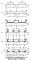
次に、本発明の第4の実施形態について説明する。図7は第4の実施形態に係る不揮発性半導体メモリの製造方法を工程順に示す概略断面図である。第4の実施形態に係る不揮発性半導体メモリの平面構成は、図2及び図3に示した第1の実施形態に係る不揮発性半導体メモリの平面構成と同様である。ここで、図7は不揮発性半導体メモリの2つのメモリセルに着目し、当該メモリセルの断面を製造工程順に示した図であって、図3の一点鎖線II−II’に沿った位置に対応する断面を示している。
【0073】
先ず、図7(a)に示すように、p型シリコン半導体基板11(比抵抗1〜12Ωcm、ホウ素(B)含有)の主表面上に、CVD法によりシリコン窒化膜12を膜厚150nm〜300nm程度に形成する。
【0074】
次に、フォトリソグラフィー及びこれに続くドライエッチングにより、ビットライン拡散層を形成する予定の領域上のシリコン窒化膜12を選択的に除去する。そして、シリコン窒化膜12をマスクとしてイオン注入を行う。具体的には、n型の不純物である砒素(As)を加速エネルギー60keV〜100keV程度、ドーズ量1×10¹⁵〜1×10¹⁶(ions/cm2 )程度の条件でイオン注入し、ビットライン拡散層となる高濃度の不純物拡散層13を形成する。
【0075】
次に、図7(b)に示すように、CVD法によりシリコン酸化膜14を膜厚300nm〜500nm程度形成し、CMP(化学機械研磨)法又はドライエッチングによりビットライン拡散層(不純物拡散層13)上のみにシリコン酸化膜14を残し、その他の領域のシリコン酸化膜14を除去する。これにより、不純物拡散層13上のシリコン酸化膜14の表面がシリコン窒化膜12の表面と略同一面となる。この図7(a)及び図7(b)に示す工程により、不純物拡散層13とシリコン酸化膜14を1回のフォトリソグラフィーで自己整合的に形成することができる。
【0076】
次に、図7(c)に示すように、リン酸等を用いたウエットエッチングによりシリコン窒化膜12を除去し、下層のp型シリコン半導体基板11の表面を露出させる。その後、p型シリコン半導体基板11に熱酸化を施して、シリコン窒化膜12を除去した結果露出したp型シリコン半導体基板11の表面に膜厚10nm〜30nm程度のシリコン酸化膜15を形成する。その後、CVD法により、シリコン酸化膜14及びシリコン酸化膜15上に、キャリアトラップ膜となるシリコン窒化膜16を膜厚10nm〜20nm程度形成する。
【0077】
次に、図7(d)に示すように、CVD法により、例えばシリコン酸化膜17を膜厚300nm〜500nm程度形成し、ドライエッチングによりシリコン酸化膜14の側壁にのみに残存するように除去する。これにより、シリコン酸化膜14の側壁にシリコン酸化膜17及びシリコン窒化膜16から成るサイドウォールが形成される。また、このドライエッチングによりサイドウォール間のシリコン窒化膜16及びシリコン酸化膜15が除去されてp型シリコン半導体基板11の表面が露出する。
【0078】
次に、図7(e)に示すように、温度800〜900℃程度、時間30〜90分程度の条件でp型シリコン半導体基板11の表面に熱酸化を施して、露出しているp型シリコン半導体基板11の表面にシリコン酸化膜18を形成する。その後、ウエットエッチングによりシリコン酸化膜17を除去し、熱酸化を施すことによりシリコン窒化膜16の表面を酸化してシリコン酸化膜19を形成する。ここで、例えば、シリコン酸化膜17中に予め不純物(ホウ素、燐)等を含有させておくことにより、シリコン酸化膜17とシリコン酸化膜14のエッチングレートを異ならせることができ、シリコン酸化膜14の除去量を最小限に抑えた状態でシリコン酸化膜17を除去することが可能である。また、シリコン酸化膜18は熱酸化により形成した酸化膜であるため、シリコン酸化膜17とはエッチングレートが異なり、その除去量は最小限に抑えられる。シリコン酸化膜17の代わりに、シリコン酸化膜14,18とはエッチングレートが異なる他の絶縁膜を用いてもよい。
【0079】
これにより、シリコン酸化膜18の両側のp型シリコン半導体基板11上において、シリコン窒化膜16は、下層がシリコン酸化膜15、上層がシリコン酸化膜19によって覆われることとなり、ゲート絶縁膜が形成される。シリコン酸化膜18を形成する熱酸化の際に、シリコン窒化膜16はシリコン酸化膜17によって覆われているため、シリコン酸化膜18の膜厚を独立して制御することが可能である。
【0080】
なお、シリコン酸化膜17をウエットエッチングによって除去した後、熱酸化を施してシリコン酸化膜18とシリコン酸化膜19を同時に形成してもよい。この場合、シリコン窒化膜16近傍では熱酸化による酸化速度が低下するため、シリコン酸化膜19はシリコン酸化膜18よりも薄く形成される。
【0081】
次に、図7(f)に示すように、CVD法により燐(P)を2×10²⁰〜6×10²⁰(atms/cm3 )程度含有した多結晶シリコン膜20を、膜厚100nm〜200nm程度形成し、フォトリソグラフィー及びこれに続くドライエッチングによりワードライン形状にパターニングする。
【0082】
その後、p型シリコン半導体基板11中の拡散層の熱処理による活性化、層間絶縁膜の形成、コンタクト孔の開孔、メタル配線の形成等を行い、本実施形態に係る不揮発性半導体メモリを完成させる。
【0083】
以上説明したように、本発明の第4の実施形態によれば、第1の実施形態と同様に、ゲート酸化膜18の両端にキャリアトラップ特性の高いシリコン窒化膜15を形成しているため、構造的に電荷の注入箇所が限定されることとなり、確実にシリコン窒化膜15の近傍のみにキャリアをトラップすることが可能となる。また、第4の実施形態によれば、不純物拡散層13と、不純物拡散層13上のシリコン酸化膜14を1回のフォトリソグラフィーで自己整合的に形成することができる。これにより、隣接する2つの不純物拡散層13間にシリコン酸化膜15,18,19及びシリコン窒化膜16から成るゲート絶縁膜を高い精度で形成することが可能となる。また、シリコン酸化膜18を形成する場合に、シリコン窒化膜16をサイドウォールであるシリコン酸化膜17によって覆うことにより、シリコン酸化膜18の膜厚を独立して高い精度で形成することが可能となる。
【0084】
なお、上述の第2〜第4の実施形態に係る不揮発性半導体メモリへのデータの書き込み、消去及び読み出しの各動作については、図4において説明した第1の実施形態と同様に行うことが可能である。
【0085】
また、上記各実施形態においては、キャリアトラップ膜としてシリコン窒化膜を用い、シリコン窒化膜の形成された部位のキャリアトラップ特性を高めた構成を例示したが、本発明はこれに限定されるものではなく、他の絶縁膜を用いる場合を含め、チャネル領域の端部におけるキャリアトラップ特性を局部的に高めた構成は全て本発明の範疇に属する。
【0086】
【発明の効果】
本発明によれば、キャリアの注入位置を異ならせて2ビットの情報を記録する半導体記憶装置において、2ビットの情報を安定かつ確実に記録し、保持することが可能となる。従って、書き込み又は消去不良の発生を抑止することができ、信頼性を向上させた半導体記憶装置及びその製造方法を提供することができる。
【図面の簡単な説明】
【図1】本発明の第1の実施形態に係る不揮発性半導体メモリの製造方法を工程順に示す概略断面図である。
【図2】本発明の各実施形態に係る不揮発性半導体メモリの平面構成を示す概略平面図である。
【図3】本発明の各実施形態に係る不揮発性半導体メモリの平面構成を詳細に示す概略平面図である。
【図4】本発明の各実施形態に係る不揮発性半導体メモリの書き込み、読み出しの動作を示す概略断面図である。
【図5】本発明の第2の実施形態に係る不揮発性半導体メモリの製造方法を工程順に示す概略断面図である。
【図6】本発明の第3の実施形態に係る不揮発性半導体メモリの製造方法を工程順に示す概略断面図である。
【図7】本発明の第4の実施形態に係る不揮発性半導体メモリの製造方法を工程順に示す概略断面図である。
【図8】従来の不揮発性半導体メモリの構成を示す概略断面図である。
【符号の説明】
1,11 p型シリコン半導体基板
2,5,7,14,15,17,18,19 シリコン酸化膜
3,4,10,12,16 シリコン窒化膜
6,13 不純物拡散層
8,20 多結晶シリコン膜
9 タングステンシリサイド膜[0001]
BACKGROUND OF THE INVENTION
The present invention relates to a semiconductor memory device and a method for manufacturing the same, and is particularly suitable for use in a nonvolatile semiconductor memory capable of recording 2-bit information in one memory cell.
[0002]
[Prior art]
In recent years, non-volatile semiconductor memories that can record 2-bit information in one memory cell by changing the carrier injection position have been researched and developed. This non-volatile semiconductor memory is a memory that captures carriers in a charge trapping film provided under the gate, and the direction of the voltage applied between the source and drain is opposite when writing and reading information. The electron traps are independently captured in the charge trapping film at positions corresponding to both ends of the channel region. Then, 2-bit information can be recorded depending on whether electrons are captured at both ends.
[0003]
For example, International Publication WO 99/07000 discloses a nonvolatile semiconductor memory having the above-described configuration. The configuration of the nonvolatile semiconductor memory and the data write / read operation disclosed in the publication will be briefly described with reference to FIG.
[0004]
As shown in FIG. 8, the
[0005]
The
[0006]
In the case of writing information to the RIGHT BIT, for example, the source is set to 0 V and the drain is set to about 5 V, a potential difference is generated between the source and the drain, and a high voltage (about 10 V) is applied to the
[0007]
When information is read from the RIGHT BIT, a voltage in the opposite direction to that in the writing is applied between the source / drain. At this time, since electrons are trapped in the
[0008]
In the case where electrons are captured in the
[0009]
Information can be written to and read from the LEFT BIT in the same manner as in the RIGHT BIT, and a voltage in a direction opposite to the direction of the voltage applied at the time of writing and reading the information to the RIGHT BIT is applied. Can be done.
[0010]
[Problems to be solved by the invention]
However, for example, when information is written to the RIGHT BIT, the channel hot electron injection position generated to raise the threshold value of the memory cell during writing varies depending on the voltage applied to the
[0011]
Further, in the state where the threshold value is raised (for example, in the writing state), the hot hole injected when the threshold value of the memory cell is lowered (for example, the erasing operation) has a different generation mechanism from the above-mentioned hot electrons. The injection positions of the two do not necessarily match. For this reason, there is a problem that either one of the charges may remain in the
[0012]
This problem can be alleviated by injecting excessive electrons when raising the threshold and injecting excessive holes when lowering the threshold. Another problem arises that the writing and erasing speeds are delayed and the performance of the device is deteriorated. In addition, excessive carrier injection causes an electrical stress more than necessary to be applied to the insulating film, which causes dielectric breakdown over time and is not desirable from the viewpoint of device reliability.
[0013]
In addition, if the method of matching the voltage application conditions during hole injection with the distribution of electron injection positions is selected, the hole generation efficiency is not necessarily optimal, and this also leads to degradation of device characteristics.
[0014]
The present invention has been made to solve such problems. In a semiconductor memory device that records 2-bit information by changing the carrier injection position, the 2-bit information is reliably recorded and held. It is an object of the present invention to provide a semiconductor memory device and a method for manufacturing the same that can improve the reliability by suppressing the occurrence of a write failure or an erase failure.
[0015]
[Means for Solving the Problems]
A semiconductor memory device according to the present invention includes a pair of impurity diffusion layers formed in a surface region of a semiconductor substrate, and a gate electrode formed on the semiconductor substrate between the pair of impurity diffusion layers via a gate insulating film. A semiconductor memory device configured to trap carriers in the gate insulating film by applying a predetermined voltage to the gate electrode, wherein the semiconductor memory device is located at a position close to each of the pair of impurity diffusion layers. A charge trapping film having a carrier trap characteristic higher than that of the gate insulating film is formed in the gate insulating film, and the gate insulating film is located at a position adjacent to each of the pair of impurity diffusion layers. Thinly formed compared to the areaThen, information of two bits is stored by injecting carriers consisting of hot electrons or hot holes into the two charge trapping films formed at positions close to the pair of impurity diffusion layers.
[0019]
In one embodiment of the semiconductor memory device of the present invention, another charge trapping film is formed on the gate insulating film, and the gate electrode is formed on the gate insulating film via the another charge trapping film. Yes.
[0020]
A method for manufacturing a semiconductor memory device of the present invention includes:The present invention relates to a method for manufacturing a semiconductor device that stores information of two bits by injecting carriers consisting of hot electrons or hot holes into two charge trapping films formed at positions close to a pair of impurity diffusion layers, respectively.A first step of sequentially forming first and second insulating films on a semiconductor substrate; a second step of selectively removing the first and second insulating films and patterning them; The second insulating film from above the semiconductor substrate;DownA third step of forming a third insulating film on the semiconductor substrate over a predetermined range, and introducing impurities into the semiconductor substrate using the second insulating film as a mask, and both sides of the second insulating film A fourth step of forming a pair of independent impurity diffusion layers in the surface region of the semiconductor substrate, and a step of forming the second insulating filmDownA fifth step of leaving the third insulating film formed in a predetermined range and removing the third insulating film in other regions to expose the semiconductor substrate, and thermally oxidizing the exposed semiconductor substrate A sixth step of forming an element isolation film, and removing the first and second insulating films to expose the underlying semiconductor substrate and the third insulating film; And forming a fourth insulating film by thermally oxidizing the exposed surface of the semiconductor substrate, and covering the upper and lower layers of the charge trapping film with the fourth insulating film. An eighth step, a ninth step of forming a conductive film on the fourth insulating film, and a tenth step of patterning the conductive film into a gate electrode shape.
[0021]
In one embodiment of the method for manufacturing a semiconductor memory device of the present invention, a predetermined amount of the first insulating film is removed in the pattern width direction between the second step and the third step, and the first step is performed. An eleventh step of making the width narrower than the pattern width of the second insulating film, and in the third step, the third step is performed on the exposed semiconductor substrate and on the semiconductor substrate in the predetermined amount range. An insulating film is formed.
[0022]
In one embodiment of the method for manufacturing a semiconductor memory device of the present invention, a twelfth insulating film is formed on the fourth insulating film between the eighth process and the ninth process. In the ninth step, the conductive film is formed on the fourth insulating film via the fifth insulating film.
[0023]
A method for manufacturing a semiconductor memory device of the present invention includes:The present invention relates to a method for manufacturing a semiconductor device that stores information of two bits by injecting carriers consisting of hot electrons or hot holes into two charge trapping films formed at positions close to a pair of impurity diffusion layers, respectively.Forming a first insulating film on the semiconductor substrate; selectively removing the first insulating film to expose the underlying semiconductor substrate; and exposing the first insulating film as a mask. Introducing an impurity into the semiconductor substrate and forming a pair of independent impurity diffusion layers in the surface region of the semiconductor substrate on both sides of the first insulating film; and on the impurity diffusion layer and the first Forming a second insulating film so as to cover the insulating film; removing the second insulating film on the first insulating film to expose the first insulating film; and the first Removing the insulating film, exposing the underlying semiconductor substrate to make this region an element active region, forming a third insulating film on the semiconductor substrate in the element active region, Forming a fourth insulating film on the third insulating film; Forming a fifth insulating film so as to cover the fourth and second insulating films; removing the fifth insulating film so as to remain only on both sides of the element active region; and Forming a sidewall made of the fifth insulating film on the side wall of the insulating film, exposing the semiconductor substrate in the element active region, and forming a sixth insulating film on the exposed semiconductor substrate. A step of removing the side wall to expose the fourth insulating film under the side wall and using the fourth insulating film as a charge trapping film; and a seventh step on the charge trapping film. A step of forming an insulating film; and a step of forming a conductive film covering the sixth and seventh insulating films.
[0024]
[Action]
Since the present invention comprises the above technical means, when a high voltage is applied to the gate electrode during data writing to generate hot electrons, electrons are generated at the end of the gate insulating film having a higher carrier trapping characteristic than the central portion of the channel width. Will be injected. This makes it possible to intensively capture electrons at the end of the gate insulating film below the gate electrode. Similarly, when erasing data, hot holes can be intensively injected into the edge of the gate insulating film, so that data can be erased stably.
[0025]
DETAILED DESCRIPTION OF THE INVENTION
Hereinafter, a configuration of a nonvolatile semiconductor memory and a manufacturing method thereof according to some embodiments of the present invention will be described together with reference to the drawings.
[0026]
(First embodiment)
First, the first embodiment will be described. FIG. 1 is a schematic cross-sectional view showing the method of manufacturing the nonvolatile semiconductor memory according to the first embodiment in the order of steps. 2 and 3 are schematic plan views showing the planar configuration of the nonvolatile semiconductor memory according to the first embodiment. Here, FIG. 1 focuses on one memory cell of the nonvolatile semiconductor memory, and shows the cross section of the memory cell in the order of the manufacturing process, corresponding to the position along the alternate long and short dash line II ′ of FIG. A cross section is shown.
[0027]
First, a predetermined well is formed on the p-type
[0028]
Thereafter, by photolithography and subsequent etching, the
[0029]
Next, as shown in FIG.Three) In a gas atmosphere, annealing is performed under the conditions of a temperature of about 950 ° C. and a time of about 20 minutes to 120 minutes. From the exposed p-type
[0030]
The
[0031]
Next, as shown in FIG. 1C, ion implantation is performed on the surface region of the p-type
[0032]
Next, as shown in FIG. 1D, the surface of the p-type
[0033]
Next, as shown in FIG. 1E, the p-type
[0034]
Next, as shown in FIG. 1F, the
[0035]
Since the
[0036]
Next, as shown in FIG. 1G, a
[0037]
Thereafter, a general wiring layer forming process is performed to complete the nonvolatile semiconductor memory according to the present embodiment. That is, an interlayer insulating film (silicon oxide film or the like) is deposited by the CVD method to cover the gate electrode composed of the
[0038]
FIG. 2 is a diagram showing an overall planar configuration of the completed nonvolatile semiconductor memory according to the present embodiment, and illustration of an interlayer insulating film and an aluminum film on the gate electrode is omitted. As shown in FIG. 2, a plurality of gate electrodes (
[0039]
FIG. 3 is an enlarged schematic view showing a region A surrounded by a two-dot chain line in FIG. 2, and a
[0040]
FIG. 4 is a schematic diagram showing data write and read operations. When writing data, as shown in FIG. 4A, the
[0041]
When erasing data, the
[0042]
When reading data, as shown in FIG. 4B, the
[0043]
Data can be written to and read from the
[0044]
As described above, according to the first embodiment of the present invention, since the
[0045]
(Second Embodiment)
Next, a second embodiment of the present invention will be described. FIG. 5 is a schematic cross-sectional view showing the method of manufacturing the nonvolatile semiconductor memory according to the second embodiment in the order of steps. The planar configuration of the nonvolatile semiconductor memory according to the second embodiment is the same as the planar configuration of the nonvolatile semiconductor memory according to the first embodiment shown in FIGS. Here, FIG. 5 focuses on one memory cell of the nonvolatile semiconductor memory, and shows the cross section of the memory cell in the order of the manufacturing process. Like the first embodiment, FIG. The cross section corresponding to the position along I ′ is shown. In FIG. 5, the same components as those in the first embodiment will be described with the same reference numerals as those in FIG.
[0046]
First, a predetermined well is formed on the p-type
[0047]
Thereafter, by photolithography and subsequent etching, the
[0048]
Next, as shown in FIG. 5B, the p-type
[0049]
The
[0050]
Next, as shown in FIG. 5C, ion implantation is performed on the surface region of the p-type
[0051]
Next, as shown in FIG. 5D, the surface of the p-type
[0052]
Next, as shown in FIG. 5E, the p-type
[0053]
Next, as shown in FIG. 5F, the
[0054]
Since the
[0055]
Next, as shown in FIG. 5G, a
[0056]
Thereafter, a general wiring layer forming step is performed to complete the nonvolatile semiconductor memory according to the present embodiment. That is, an interlayer insulating film (silicon oxide film or the like) is deposited by the CVD method to cover the gate electrode composed of the
[0057]
As described above, according to the second embodiment of the present invention, the
[0058]
(Third embodiment)
Next, a third embodiment of the present invention will be described. FIG. 6 is a schematic cross-sectional view showing the method of manufacturing the nonvolatile semiconductor memory according to the third embodiment in the order of steps. The planar configuration of the nonvolatile semiconductor memory according to the second embodiment is the same as the planar configuration of the nonvolatile semiconductor memory according to the first embodiment shown in FIGS. Here, FIG. 6 focuses on one memory cell of the nonvolatile semiconductor memory, and shows the cross section of the memory cell in the order of the manufacturing process. Like the first embodiment, FIG. A cross section corresponding to a position along I ′ is shown. In FIG. 6, the same components as those in the first embodiment will be described with the same reference numerals as those in FIG.
[0059]
First, a predetermined well is formed on the p-type
[0060]
Thereafter, by photolithography and subsequent etching, the
[0061]
Next, as shown in FIG. 6B, ammonia (NHThree) In a gas atmosphere, annealing is performed under the conditions of a temperature of about 950 ° C. and a time of about 20 minutes to 120 minutes. From the exposed p-type
[0062]
The
[0063]
Next, as shown in FIG. 6C, ion implantation is performed on the surface region of the p-type
[0064]
Next, as shown in FIG. 6D, the surface of the p-type
[0065]
Next, as shown in FIG. 6E, the p-type
[0066]
Next, as shown in FIG. 6F, the
[0067]
Since the
[0068]
Next, as shown in FIG. 6G, a
[0069]
Thereafter, a
[0070]
Thereafter, a general wiring layer forming step is performed to complete the nonvolatile semiconductor memory according to the present embodiment. That is, an interlayer insulating film (silicon oxide film or the like) is deposited by the CVD method to cover the gate electrode composed of the
[0071]
As described above, according to the third embodiment of the present invention, the
[0072]
(Fourth embodiment)
Next, a fourth embodiment of the present invention will be described. FIG. 7 is a schematic cross-sectional view showing the method of manufacturing the nonvolatile semiconductor memory according to the fourth embodiment in the order of steps. The planar configuration of the nonvolatile semiconductor memory according to the fourth embodiment is the same as the planar configuration of the nonvolatile semiconductor memory according to the first embodiment shown in FIGS. Here, FIG. 7 focuses on two memory cells of the nonvolatile semiconductor memory, and shows the cross sections of the memory cells in the order of the manufacturing process, corresponding to the position along the alternate long and short dash line II-II ′ of FIG. A cross section is shown.
[0073]
First, as shown in FIG. 7A, a
[0074]
Next, the
[0075]
Next, as shown in FIG. 7B, a
[0076]
Next, as shown in FIG. 7C, the
[0077]
Next, as shown in FIG. 7D, for example, a
[0078]
Next, as shown in FIG. 7E, the p-type
[0079]
Thus, on the p-type
[0080]
Alternatively, after the
[0081]
Next, as shown in FIG. 7F, phosphorus (P) is added by 2 × 10 2 by CVD.20~ 6 × 10²⁰(Atms / cmThree) A
[0082]
Thereafter, activation of the diffusion layer in the p-type
[0083]
As described above, according to the fourth embodiment of the present invention, the
[0084]
Note that data write, erase, and read operations to the nonvolatile semiconductor memory according to the second to fourth embodiments described above can be performed in the same manner as in the first embodiment described with reference to FIG. It is.
[0085]
In each of the above embodiments, the silicon nitride film is used as the carrier trap film, and the carrier trap characteristic at the portion where the silicon nitride film is formed is exemplified. However, the present invention is not limited to this. In addition, all configurations in which the carrier trap characteristics at the end of the channel region are locally enhanced, including the case where other insulating films are used, belong to the category of the present invention.
[0086]
【The invention's effect】
According to the present invention, it is possible to stably and reliably record and hold 2-bit information in a semiconductor memory device that records 2-bit information at different carrier injection positions. Therefore, it is possible to provide a semiconductor memory device and a method for manufacturing the semiconductor memory device that can suppress the occurrence of writing or erasing defects and have improved reliability.
[Brief description of the drawings]
FIG. 1 is a schematic cross-sectional view showing a method of manufacturing a nonvolatile semiconductor memory according to a first embodiment of the present invention in the order of steps.
FIG. 2 is a schematic plan view showing a planar configuration of a nonvolatile semiconductor memory according to each embodiment of the present invention.
FIG. 3 is a schematic plan view showing in detail a planar configuration of the nonvolatile semiconductor memory according to each embodiment of the present invention.
FIG. 4 is a schematic cross-sectional view showing write and read operations of the nonvolatile semiconductor memory according to each embodiment of the present invention.
FIG. 5 is a schematic cross-sectional view showing the method of manufacturing the nonvolatile semiconductor memory according to the second embodiment of the present invention in the order of steps.
FIG. 6 is a schematic cross-sectional view showing a method of manufacturing a nonvolatile semiconductor memory according to a third embodiment of the present invention in the order of steps.
FIG. 7 is a schematic cross-sectional view showing a method of manufacturing a nonvolatile semiconductor memory according to a fourth embodiment of the present invention in the order of steps.
FIG. 8 is a schematic cross-sectional view showing a configuration of a conventional nonvolatile semiconductor memory.
[Explanation of symbols]
1,11 p-type silicon semiconductor substrate
2, 5, 7, 14, 15, 17, 18, 19 Silicon oxide film
3, 4, 10, 12, 16 Silicon nitride film
6,13 Impurity diffusion layer
8,20 Polycrystalline silicon film
9 Tungsten silicide film
Claims (6)
前記1対の不純物拡散層間における前記半導体基板上にゲート絶縁膜を介して形成されたゲート電極とを備え、
前記ゲート電極に所定電圧を印加することにより前記ゲート絶縁膜にキャリアを捕獲するように成された半導体記憶装置であって、
前記1対の不純物拡散層のそれぞれに近接する位置における前記ゲート絶縁膜中に、前記ゲート絶縁膜に比してキャリアトラップ特性が高い電荷捕獲膜が形成されており、
前記ゲート絶縁膜は、前記1対の不純物拡散層のそれぞれに近接する位置が他の領域に比して薄く形成されており、
ホットエレクトロン又はホットホールからなるキャリアを前記1対の不純物拡散層に近接する位置に形成された2つの前記電荷捕獲膜にそれぞれ注入することによって2つのビットの情報を記憶することを特徴とする半導体記憶装置。A pair of impurity diffusion layers formed in the surface region of the semiconductor substrate;
A gate electrode formed on the semiconductor substrate between the pair of impurity diffusion layers via a gate insulating film;
A semiconductor memory device configured to capture carriers in the gate insulating film by applying a predetermined voltage to the gate electrode,
A charge trapping film having a higher carrier trap characteristic than the gate insulating film is formed in the gate insulating film at a position close to each of the pair of impurity diffusion layers,
The gate insulating film is formed so that a position adjacent to each of the pair of impurity diffusion layers is thinner than other regions ,
Information of two bits is stored by injecting carriers consisting of hot electrons or hot holes into the two charge trapping films formed at positions close to the pair of impurity diffusion layers, respectively. Storage device.
前記第1及び第2の絶縁膜を選択的に除去して共にパターニングする第2の工程と、
露出した前記半導体基板上から前記第2の絶縁膜の下方の所定範囲にかけての前記半導体基板上に第3の絶縁膜を形成する第3の工程と、
前記第2の絶縁膜をマスクとして前記半導体基板に不純物を導入し、前記第2の絶縁膜の両側の前記半導体基板の表面領域に各々が独立した一対の不純物拡散層を形成する第4の工程と、
前記第2の絶縁膜の下方の所定範囲に形成された前記第3の絶縁膜を残し、他の領域の前記第3の絶縁膜を除去して前記半導体基板を露出させる第5の工程と、
露出した前記半導体基板を熱酸化して素子分離膜を形成する第6の工程と、
前記第1及び第2の絶縁膜を除去して、下層の前記半導体基板及び前記第3の絶縁膜を露出させ、当該第3の絶縁膜を電荷捕獲膜とする第7の工程と、
露出した前記半導体基板の表面を熱酸化して第4の絶縁膜を形成し、前記電荷捕獲膜の上層及び下層を当該第4の絶縁膜で覆う第8の工程と、
前記第4の絶縁膜の上層に導電膜を形成する第9の工程と、
前記導電膜をゲート電極形状にパターニングする第10の工程とを有することを特徴とするホットエレクトロン又はホットホールからなるキャリアを前記一対の不純物拡散層に近接する位置に形成された2つの前記電荷捕獲膜にそれぞれ注入することによって2つのビットの情報を記憶する半導体記憶装置の製造方法。A first step of sequentially forming first and second insulating films on a semiconductor substrate;
A second step of selectively removing the first and second insulating films and patterning them together;
A third step of forming a third insulating film on the semiconductor substrate from the exposed semiconductor substrate to a predetermined range below the second insulating film;
A fourth step of introducing impurities into the semiconductor substrate using the second insulating film as a mask, and forming a pair of independent impurity diffusion layers in the surface regions of the semiconductor substrate on both sides of the second insulating film; When,
A fifth step of leaving the third insulating film formed in a predetermined range below the second insulating film and removing the third insulating film in another region to expose the semiconductor substrate;
A sixth step of thermally oxidizing the exposed semiconductor substrate to form an element isolation film;
Removing the first and second insulating films, exposing the underlying semiconductor substrate and the third insulating film, and using the third insulating film as a charge trapping film;
An eighth step of thermally oxidizing the exposed surface of the semiconductor substrate to form a fourth insulating film, and covering an upper layer and a lower layer of the charge trapping film with the fourth insulating film;
A ninth step of forming a conductive film on the fourth insulating film;
And the tenth step of patterning the conductive film into the shape of a gate electrode . The two charge traps formed at positions adjacent to the pair of impurity diffusion layers by carriers made of hot electrons or hot holes. A method of manufacturing a semiconductor memory device that stores information of two bits by injecting each into a film .
前記第3の工程において、露出した前記半導体基板上及び前記所定量の範囲における前記半導体基板上に前記第3の絶縁膜を形成することを特徴とする請求項3に記載の半導体記憶装置の製造方法。Between the second step and the third step, a predetermined amount of the first insulating film is removed in the pattern width direction to make the width narrower than the pattern width of the second insulating film. And further comprising a step
4. The method of manufacturing a semiconductor memory device according to claim 3 , wherein, in the third step, the third insulating film is formed on the exposed semiconductor substrate and on the semiconductor substrate in the predetermined amount range. Method.
前記第9の工程において前記第4の絶縁膜上に前記第5の絶縁膜を介して前記導電膜を形成することを特徴とする請求項3に記載の半導体記憶装置の製造方法。Further comprising a twelfth step of forming a fifth insulating film on the fourth insulating film between the eighth step and the ninth step,
4. The method of manufacturing a semiconductor memory device according to claim 3 , wherein in the ninth step, the conductive film is formed on the fourth insulating film via the fifth insulating film.
前記第1の絶縁膜を選択的に除去して下層の前記半導体基板を露出させる工程と、
前記第1の絶縁膜をマスクとして露出した前記半導体基板に不純物を導入し、
前記第1の絶縁膜の両側の前記半導体基板の表面領域に各々が独立した一対の不純物拡散層を形成する工程と、
前記不純物拡散層上及び前記第1の絶縁膜を覆うように第2の絶縁膜を形成する工程と、
前記第1の絶縁膜上の前記第2の絶縁膜を除去し、前記第1の絶縁膜を露出させる工程と、
前記第1の絶縁膜を除去して下層の前記半導体基板を露出させ、この領域を素子活性領域とする工程と、
前記素子活性領域における前記半導体基板上に第3の絶縁膜を形成する工程と、
前記第3の絶縁膜上に第4の絶縁膜を形成する工程と、
前記第4及び第2の絶縁膜を覆うように第5の絶縁膜を形成する工程と、
前記素子活性領域の両側にのみ残存するように前記第5の絶縁膜を除去して、
前記第2の絶縁膜の側壁に前記第5の絶縁膜から成るサイドウォールを形成するとともに、前記素子活性領域における前記半導体基板を露出させる工程と、
露出した前記半導体基板上に第6の絶縁膜を形成する工程と、
前記サイドウォールを除去して前記サイドウォールの下層の前記第4の絶縁膜を露出させ、当該第4の絶縁膜を電荷捕獲膜とする工程と、
前記電荷捕獲膜上に第7の絶縁膜を形成する工程と、
前記第6及び第7の絶縁膜上を覆う導電膜を形成する工程とを有することを特徴とするホットエレクトロン又はホットホールからなるキャリアを前記一対の不純物拡散層に近接する位置に形成された2つの前記電荷捕獲膜にそれぞれ注入することによって2つのビットの情報を記憶する半導体記憶装置の製造方法。Forming a first insulating film on the semiconductor substrate;
Selectively removing the first insulating film to expose the underlying semiconductor substrate;
Impurities are introduced into the exposed semiconductor substrate using the first insulating film as a mask,
Forming a pair of independent impurity diffusion layers in the surface region of the semiconductor substrate on both sides of the first insulating film;
Forming a second insulating film so as to cover the impurity diffusion layer and the first insulating film;
Removing the second insulating film on the first insulating film and exposing the first insulating film;
Removing the first insulating film to expose the underlying semiconductor substrate, and making this region an element active region;
Forming a third insulating film on the semiconductor substrate in the element active region;
Forming a fourth insulating film on the third insulating film;
Forming a fifth insulating film so as to cover the fourth and second insulating films;
Removing the fifth insulating film so as to remain only on both sides of the element active region;
Forming a sidewall made of the fifth insulating film on a side wall of the second insulating film, and exposing the semiconductor substrate in the element active region;
Forming a sixth insulating film on the exposed semiconductor substrate;
Removing the side wall to expose the fourth insulating film under the side wall, and using the fourth insulating film as a charge trapping film;
Forming a seventh insulating film on the charge trapping film;
Forming a conductive film covering the sixth and seventh insulating films, and forming a carrier made of hot electrons or hot holes at a position close to the pair of impurity diffusion layers. A method of manufacturing a semiconductor memory device, wherein information of two bits is stored by being injected into each of the two charge trapping films .
Priority Applications (4)
| Application Number | Priority Date | Filing Date | Title |
|---|---|---|---|
| JP25078099A JP3958899B2 (en) | 1999-09-03 | 1999-09-03 | Semiconductor memory device and manufacturing method thereof |
| KR1020027002754A KR100727445B1 (en) | 1999-09-03 | 2000-05-30 | Semiconductor memory and method of manufacture thereof |
| PCT/JP2000/003468 WO2001018878A1 (en) | 1999-09-03 | 2000-05-30 | Semiconductor memory and method of manufacture thereof |
| US10/085,023 US6750520B2 (en) | 1999-09-03 | 2002-03-01 | Two-bit semiconductor memory with enhanced carrier trapping |
Applications Claiming Priority (1)
| Application Number | Priority Date | Filing Date | Title |
|---|---|---|---|
| JP25078099A JP3958899B2 (en) | 1999-09-03 | 1999-09-03 | Semiconductor memory device and manufacturing method thereof |
Publications (3)
| Publication Number | Publication Date |
|---|---|
| JP2001077215A JP2001077215A (en) | 2001-03-23 |
| JP2001077215A5 JP2001077215A5 (en) | 2004-12-09 |
| JP3958899B2 true JP3958899B2 (en) | 2007-08-15 |
Family
ID=17212945
Family Applications (1)
| Application Number | Title | Priority Date | Filing Date |
|---|---|---|---|
| JP25078099A Expired - Fee Related JP3958899B2 (en) | 1999-09-03 | 1999-09-03 | Semiconductor memory device and manufacturing method thereof |
Country Status (4)
| Country | Link |
|---|---|
| US (1) | US6750520B2 (en) |
| JP (1) | JP3958899B2 (en) |
| KR (1) | KR100727445B1 (en) |
| WO (1) | WO2001018878A1 (en) |
Families Citing this family (14)
| Publication number | Priority date | Publication date | Assignee | Title |
|---|---|---|---|---|
| JP4923321B2 (en) * | 2000-09-12 | 2012-04-25 | ソニー株式会社 | Method of operating nonvolatile semiconductor memory device |
| SG95637A1 (en) | 2001-03-15 | 2003-04-23 | Micron Technology Inc | Semiconductor/printed circuit board assembly, and computer system |
| JP4670187B2 (en) * | 2001-06-06 | 2011-04-13 | ソニー株式会社 | Nonvolatile semiconductor memory device |
| DE10201304A1 (en) | 2002-01-15 | 2003-07-31 | Infineon Technologies Ag | Non-volatile semiconductor memory cell and associated manufacturing process |
| US6614694B1 (en) * | 2002-04-02 | 2003-09-02 | Macronix International Co., Ltd. | Erase scheme for non-volatile memory |
| JP3664159B2 (en) * | 2002-10-29 | 2005-06-22 | セイコーエプソン株式会社 | Semiconductor device and manufacturing method thereof |
| JP2004266185A (en) * | 2003-03-04 | 2004-09-24 | Renesas Technology Corp | Semiconductor device and its manufacturing method |
| WO2005122246A1 (en) * | 2004-06-14 | 2005-12-22 | Spansion Llc | Semiconductor device and semiconductor device manufacturing method |
| JP4872395B2 (en) * | 2006-03-15 | 2012-02-08 | ヤマハ株式会社 | Silicon oxide film forming method, capacitor element manufacturing method, and semiconductor device manufacturing method |
| JP2008053270A (en) * | 2006-08-22 | 2008-03-06 | Nec Electronics Corp | Semiconductor memory device, and its manufacturing method |
| JP2008227403A (en) * | 2007-03-15 | 2008-09-25 | Spansion Llc | Semiconductor device and its manufacturing method |
| US8283224B2 (en) * | 2008-12-23 | 2012-10-09 | Texas Instruments Incorporated | Ammonia pre-treatment in the fabrication of a memory cell |
| JP5552521B2 (en) * | 2012-11-09 | 2014-07-16 | スパンション エルエルシー | Manufacturing method of semiconductor device |
| US10290352B2 (en) * | 2015-02-27 | 2019-05-14 | Qualcomm Incorporated | System, apparatus, and method of programming a one-time programmable memory circuit having dual programming regions |
Family Cites Families (10)
| Publication number | Priority date | Publication date | Assignee | Title |
|---|---|---|---|---|
| JPS4873086A (en) * | 1971-11-24 | 1973-10-02 | ||
| DE2932712A1 (en) | 1979-08-13 | 1981-03-26 | Basf Ag, 67063 Ludwigshafen | METHOD FOR OBTAINING IMIDAZOLES |
| JPS5632464U (en) * | 1979-08-17 | 1981-03-30 | ||
| JPS60161674A (en) * | 1984-02-02 | 1985-08-23 | Matsushita Electronics Corp | Semiconductor memory device |
| US5143860A (en) * | 1987-12-23 | 1992-09-01 | Texas Instruments Incorporated | High density EPROM fabricaiton method having sidewall floating gates |
| JPH05145080A (en) * | 1991-11-25 | 1993-06-11 | Kawasaki Steel Corp | Nonvolatile storage device |
| JP3397903B2 (en) * | 1994-08-23 | 2003-04-21 | 新日本製鐵株式会社 | Manufacturing method of nonvolatile semiconductor memory device |
| KR100187656B1 (en) | 1995-05-16 | 1999-06-01 | 김주용 | Method for manufacturing a flash eeprom and the programming method |
| US5768192A (en) * | 1996-07-23 | 1998-06-16 | Saifun Semiconductors, Ltd. | Non-volatile semiconductor memory cell utilizing asymmetrical charge trapping |
| US6768165B1 (en) | 1997-08-01 | 2004-07-27 | Saifun Semiconductors Ltd. | Two bit non-volatile electrically erasable and programmable semiconductor memory cell utilizing asymmetrical charge trapping |
-
1999
- 1999-09-03 JP JP25078099A patent/JP3958899B2/en not_active Expired - Fee Related
-
2000
- 2000-05-30 KR KR1020027002754A patent/KR100727445B1/en not_active IP Right Cessation
- 2000-05-30 WO PCT/JP2000/003468 patent/WO2001018878A1/en active Application Filing
-
2002
- 2002-03-01 US US10/085,023 patent/US6750520B2/en not_active Expired - Fee Related
Also Published As
| Publication number | Publication date |
|---|---|
| KR100727445B1 (en) | 2007-06-13 |
| US6750520B2 (en) | 2004-06-15 |
| WO2001018878A1 (en) | 2001-03-15 |
| KR20020026003A (en) | 2002-04-04 |
| JP2001077215A (en) | 2001-03-23 |
| US20020084484A1 (en) | 2002-07-04 |
Similar Documents
| Publication | Publication Date | Title |
|---|---|---|
| US5338954A (en) | Semiconductor memory device having an insulating film and a trap film joined in a channel region | |
| JP3973819B2 (en) | Semiconductor memory device and manufacturing method thereof | |
| JP4325972B2 (en) | Manufacturing method of semiconductor integrated circuit device including nonvolatile semiconductor memory device | |
| JP3496932B2 (en) | Semiconductor integrated circuit device including nonvolatile semiconductor memory device | |
| JP3983094B2 (en) | Method for manufacturing nonvolatile semiconductor memory device | |
| JP3967193B2 (en) | Nonvolatile semiconductor memory device and manufacturing method thereof | |
| JP4152598B2 (en) | Manufacturing method of semiconductor device | |
| JP2882392B2 (en) | Nonvolatile semiconductor memory device and method of manufacturing the same | |
| JP3958899B2 (en) | Semiconductor memory device and manufacturing method thereof | |
| JP3430084B2 (en) | Manufacturing method of nonvolatile semiconductor memory device | |
| JP2006108620A (en) | Nonvolatile memory device containing conductive side wall spacer and its manufacturing method | |
| JP2004193226A (en) | Nonvolatile semiconductor memory device and method of manufacturing the same | |
| JP5486884B2 (en) | Nonvolatile semiconductor memory device and manufacturing method thereof | |
| KR20030081622A (en) | Non-volitile memory device and method thereof | |
| JP2956549B2 (en) | Semiconductor memory device, manufacturing method thereof and data erasing method | |
| US7220651B2 (en) | Transistor and method for manufacturing the same | |
| JP2007158093A (en) | Nonvolatile semiconductor memory device, and manufacturing method thereof | |
| JPWO2007000808A1 (en) | Semiconductor device and manufacturing method thereof | |
| JP4334315B2 (en) | Manufacturing method of semiconductor memory device | |
| JP3016607B2 (en) | Manufacturing method of nonvolatile memory | |
| JP5162129B2 (en) | Semiconductor device | |
| JP2003243544A (en) | Non-volatile semiconductor storage and manufacturing method thereof | |
| JP3807633B2 (en) | Method for manufacturing nonvolatile semiconductor memory device | |
| JP3062043B2 (en) | Nonvolatile memory and manufacturing method thereof | |
| JP3137091B2 (en) | Manufacturing method of nonvolatile semiconductor memory device |
Legal Events
| Date | Code | Title | Description |
|---|---|---|---|
| A711 | Notification of change in applicant |
Free format text: JAPANESE INTERMEDIATE CODE: A711 Effective date: 20060522 |
|
| A711 | Notification of change in applicant |
Free format text: JAPANESE INTERMEDIATE CODE: A711 Effective date: 20060701 |
|
| A131 | Notification of reasons for refusal |
Free format text: JAPANESE INTERMEDIATE CODE: A131 Effective date: 20070306 |
|
| A521 | Request for written amendment filed |
Free format text: JAPANESE INTERMEDIATE CODE: A523 Effective date: 20070410 |
|
| TRDD | Decision of grant or rejection written | ||
| A01 | Written decision to grant a patent or to grant a registration (utility model) |
Free format text: JAPANESE INTERMEDIATE CODE: A01 Effective date: 20070502 |
|
| A61 | First payment of annual fees (during grant procedure) |
Free format text: JAPANESE INTERMEDIATE CODE: A61 Effective date: 20070511 |
|
| R150 | Certificate of patent or registration of utility model |
Free format text: JAPANESE INTERMEDIATE CODE: R150 |
|
| FPAY | Renewal fee payment (event date is renewal date of database) |
Free format text: PAYMENT UNTIL: 20100518 Year of fee payment: 3 |
|
| FPAY | Renewal fee payment (event date is renewal date of database) |
Free format text: PAYMENT UNTIL: 20110518 Year of fee payment: 4 |
|
| FPAY | Renewal fee payment (event date is renewal date of database) |
Free format text: PAYMENT UNTIL: 20120518 Year of fee payment: 5 |
|
| FPAY | Renewal fee payment (event date is renewal date of database) |
Free format text: PAYMENT UNTIL: 20130518 Year of fee payment: 6 |
|
| FPAY | Renewal fee payment (event date is renewal date of database) |
Free format text: PAYMENT UNTIL: 20130518 Year of fee payment: 6 |
|
| RD02 | Notification of acceptance of power of attorney |
Free format text: JAPANESE INTERMEDIATE CODE: R3D02 |
|
| FPAY | Renewal fee payment (event date is renewal date of database) |
Free format text: PAYMENT UNTIL: 20130518 Year of fee payment: 6 |
|
| R250 | Receipt of annual fees |
Free format text: JAPANESE INTERMEDIATE CODE: R250 |
|
| R250 | Receipt of annual fees |
Free format text: JAPANESE INTERMEDIATE CODE: R250 |
|
| R250 | Receipt of annual fees |
Free format text: JAPANESE INTERMEDIATE CODE: R250 |
|
| S111 | Request for change of ownership or part of ownership |
Free format text: JAPANESE INTERMEDIATE CODE: R313111 |
|
| R350 | Written notification of registration of transfer |
Free format text: JAPANESE INTERMEDIATE CODE: R350 |
|
| LAPS | Cancellation because of no payment of annual fees |