JP3952811B2 - Piezoelectric vibrating piece, method for manufacturing piezoelectric vibrating piece, and piezoelectric device - Google Patents
Piezoelectric vibrating piece, method for manufacturing piezoelectric vibrating piece, and piezoelectric device Download PDFInfo
- Publication number
- JP3952811B2 JP3952811B2 JP2002065875A JP2002065875A JP3952811B2 JP 3952811 B2 JP3952811 B2 JP 3952811B2 JP 2002065875 A JP2002065875 A JP 2002065875A JP 2002065875 A JP2002065875 A JP 2002065875A JP 3952811 B2 JP3952811 B2 JP 3952811B2
- Authority
- JP
- Japan
- Prior art keywords
- vibrating piece
- piezoelectric vibrating
- reverse mesa
- end point
- reverse
- Prior art date
- Legal status (The legal status is an assumption and is not a legal conclusion. Google has not performed a legal analysis and makes no representation as to the accuracy of the status listed.)
- Expired - Fee Related
Links
Images


Description
【0001】
【発明の属する技術分野】
本発明は、圧電振動片、その製造方法および圧電デバイスに関するものである。
【0002】
【従来の技術】
電気回路において一定の周波数を得るため、ATカット圧電振動片を実装した圧電デバイスが広く利用されている。一般に、ATカット圧電振動片は、水晶等の圧電材料におけるXZ平面をX軸周りに一定角度回転させた平面を想定し、この平面に沿って切り出した圧電基板から形成されるものである。
【0003】
近年では、高い共振周波数を有する圧電デバイスが要求されている。一般に、圧電振動片の厚さが薄いほど圧電デバイスの共振周波数は高くなるので、例えば100MHz以上の共振周波数を得るためには、圧電振動片の厚さを16μm以下とする必要がある。しかし圧電振動片が極端に薄くなると、加工自体が難しくなることに加え、衝撃力に対する剛性が弱くなる。
【0004】
そこで、逆メサ型圧電振動片が提案されている。図15に逆メサ型圧電振動片の説明図を示す。同図(1)は平面図であり、同図(2)はF−F線における正面断面図である。逆メサ型圧電振動片100は、励振電極120を形成する振動部102の厚さを薄くすることにより高周波での共振を可能とする一方で、その周縁部104の厚さを厚くすることにより剛性を確保したものである。一例をあげれば、周縁部104の厚さは100μm程度に形成し、振動部102の厚さは10μm程度に形成する。
【0005】
上述した逆メサ部はエッチングにより形成する。ここで、水晶等の圧電材料は、その結晶方位によりエッチングレートに異方性を有する。そのため、図15(2)のように逆メサ部110が形成されると考えられていた。すなわち、逆メサ部110の+Y′側端部には急斜面114が形成され、−Y′側端部には垂直面115等が形成されて、急斜面114と垂直面115等との間には、すべて水平面112が形成されると考えられていた。
【0006】
そして、一対の励振電極が平行に配置されていない場合には、不要な振動が多く発生するので、逆メサ部の傾斜面を避けて励振電極を配置する必要がある。そこで、特開2001−203449号公報では、図16(1)に示す逆メサ部210を、矢印211のように移動させることにより、図16(2)に示すように、励振電極220を配置する平行部分Pを、広く確保する構造が提案されている。
【0007】
【発明が解決しようとする課題】
ところが、発明者の実験によれば、図1(2)のように逆メサ部が形成されることが明らかになった。すなわち、+Y′側の逆メサ部の−Z′側端部には、+Z′側端部の急斜面14に比べてZ′方向長さの長い、緩斜面16が形成されることが確認された。そして、この緩斜面16の表面に励振電極の一部を形成すると、励振電極が平行に配置されずに、図14(1)のQ部に示すように、不要な振動が多く発生するという問題がある。
【0008】
これを前提にして、図16に示す特開2001−203449号公報で提案された構造をみれば、矢印211の方向に逆メサ部を移動させると、励振電極を配置する平行部分がかえって減少することになり、不要な振動を発生させるおそれがある。
【0009】
本発明は上記問題点に着目し、励振電極を平行に配置することが可能であり、不要な振動を発生させることのない、圧電振動片およびその製造方法の提供を目的とする。
また本発明は、不要な振動を発生させることのない圧電デバイスの提供を目的とする。
【0010】
【課題を解決するための手段】
上記目的を達成するため、本発明に係る圧電振動片は、結晶軸(X,Y′,Z′)を有するATカット圧電振動片の、±Y′側主面にそれぞれエッチングにより形成された急斜面、緩斜面および該急斜面、緩斜面との間に水平面を有する逆メサ部を形成し、前記各逆メサ部にそれぞれ励振電極を配置した、逆メサ型ATカット圧電振動片であって、
【数7】
![]()
【数8】
![]()
【0011】
これにより、逆メサ型圧電振動片の振動部に、平行部分を広く確保することができる。したがって、励振電極を平行に配置することが可能となり、不要な振動を発生させることがない。
【0012】
また、本発明に係る圧電振動片は、結晶軸(X,Y′,Z′)を有するATカット圧電振動片の、±Y′側主面にそれぞれエッチングにより形成された急斜面、緩斜面および該急斜面、緩斜面との間に水平面を有する逆メサ部を形成し、前記各逆メサ部にそれぞれ励振電極を配置した、逆メサ型ATカット圧電振動片であって、
【数9】
![]()
【0013】
また、本発明に係る圧電振動片の製造方法は、結晶軸(X,Y′,Z′)を有するATカット圧電振動片の、±Y′側主面にそれぞれエッチングにより形成された急斜面、緩斜面および該急斜面、緩斜面との間に水平面を有する逆メサ部を形成し、前記各逆メサ部にそれぞれ励振電極を配置する、逆メサ型ATカット圧電振動片につき、圧電基板の±Y′側にフォトマスクを配置してフォトリソグラフィを行うことにより、前記各逆メサ部を形成する、逆メサ型ATカット圧電振動片の製造方法であって、
【数10】
![]()
【数11】
![]()
これにより、励振電極を平行に配置することが可能となり、不要な振動を発生させることがない。
【0014】
また、本発明に係る圧電振動片の他の製造方法は、結晶軸(X,Y′,Z′)を有するATカット圧電振動片の、±Y′側主面にそれぞれエッチングにより形成された急斜面、緩斜面および該急斜面、緩斜面との間に水平面を有する逆メサ部を形成し、前記各逆メサ部にそれぞれ励振電極を配置する、逆メサ型ATカット圧電振動片につき、圧電基板の±Y′側にフォトマスクを配置してフォトリソグラフィを行うことにより、前記各励振電極を形成する、逆メサ型ATカット圧電振動片の製造方法であって、
【数12】
![]()
【0015】
一方、本発明に係る圧電デバイスは、上述に記載の圧電振動片を使用して製造した構成とした。これにより、不要な振動を発生させることのない圧電デバイスを提供することができる。
【0016】
【発明の実施の形態】
本発明に係る圧電振動片、その製造方法および圧電デバイスの好ましい実施の形態を、添付図面に従って詳細に説明する。なお以下に記載するのは本発明の実施形態の一態様にすぎず、本発明はこれらに限定されるものではない。
【0017】
本発明は、逆メサ型ATカット圧電振動片の逆メサ部を、エッチングによって形成する場合に、逆メサ部のZ′方向両端部に斜面が形成されるという知見に基づいている。図1に逆メサ部に形成される斜面の説明図を示す。一般に、水晶等の圧電材料は三方晶系であり、同図(1)に示す結晶軸を有する。図中のX軸は電気軸であり、Y軸は機械軸であり、Z軸は光軸である。ATカット圧電振動片30は、同図(1)の座標系におけるXZ平面を、X軸周りに角度θだけ回転させた平面に沿って、圧電材料から切り出された平板である。なお、Y軸およびZ軸もX軸周りにθ回転させて、それぞれY′軸およびZ′軸とする。したがって、ATカット圧電振動片30は、結晶軸(X,Y′,Z′)を有する。
【0018】
このATカット圧電振動片30は、Y′軸に直交する面が励振面(主面)となるので、±Y′側主面の中心部付近に、エッチングにより凹部(逆メサ部)を形成する。すると、図1(2)に示すように、逆メサ部のZ′方向両端部に斜面が形成される。そのうち、+Y′側の逆メサ部10において、+Z′側端部に形成される急斜面14は、従来からその存在が知られていたものである。この急斜面14は、上述したように圧電材料が三方晶系であって、Z方向よりY方向のエッチングレートが低くなるために形成されるものと考えられる。一方、−Z′側端部に形成される緩斜面16は、今回初めてその存在が確認されたものである。発明者の実験によれば、この緩斜面16は、あらゆる大きさの圧電振動片において規則的に形成されることが確認された。以下に、その実験の内容を詳述する。
【0019】
実験は、逆メサ部のエッチングが進むにつれて、逆メサ部のZ′方向の形状がどのように変化するかを測定することにより行った。実験には、図1(1)にθで示すカット角が35゜13′30″のATカット水晶振動片を使用した。なお、実験サンプルとして、あらゆる大きさの水晶振動片を使用した。表1に、実験サンプルとして使用した水晶振動片の逆メサ部の外形を示す。なお、水晶振動片の厚さはいずれも0.1mm(100μm)である。
【表1】

エッチングは、ウエットエッチングによって行った。エッチング液には、フッ酸とフッ化アンモニウムとを重量比1:1で混合した液体を使用した。一方、逆メサ部の形状測定は、非接触3次元形状測定装置を使用して行った。
【0021】
具体的な実験手順について、図9および図10を使用して説明する。まず、図9(1)に示すように、水晶振動片61の表面全体に、耐蝕膜であるAu/Cr膜62を、スパッタ法によって形成する。さらに、Au/Cr膜62の表面全体に、レジスト64を塗布する。次に、図9(2)に示すように、逆メサ部10に相当する部分が透光部71aとなっているフォトマスク70aを使用して、水晶振動片61の+Y′側のみレジスト64を露光する。さらに、図9(3)に示すように、逆メサ部10のレジスト64を現像して除去する。次に、図10(1)に示すように、パターニングされたレジスト64をマスクとして、逆メサ部10のAu/Cr膜62をエッチングする。以上により、水晶振動片61の逆メサ部10をエッチングするためのマスクが形成される。
【0022】
次に、上記のように形成したマスクを使用して、水晶振動片の逆メサ部に対し1回目のエッチングを行う。ここでは、逆メサ部の最深部の深さが10μm程度となるように、時間管理をしつつエッチングを行う。次に、3次元形状測定装置を使用して、逆メサ部のZ′方向の形状を測定し記録する。さらに、同一部分に対して2回目のエッチングを行い、形状を測定する。このようにして、エッチングと3次元形状測定とを4回にわたって繰り返すことにより、エッチングが進むにつれて、逆メサ部のZ′方向の形状がどのように変化するかを測定する。なお、各実験サンプルに対して上記と同じ実験を行う。
【0023】
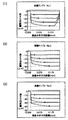
各実験サンプルに対する実験結果を、図2および図3の各図に示す。なお図3は、図2の原点付近の拡大図である。図2および図3の各図では、横軸に逆メサ部の水平(Z′)方向距離を取り、縦軸に逆メサ部の深さ(Y′)方向距離を取っている。また各図では、上から順に、1回目から4回目のエッチング後の形状測定結果を、重ねて記載している。なお、各形状測定結果における水平方向および深さ方向の原点は、逆メサ部の−Z′方向端点とした。なお、エッチングにより逆メサ部は、わずかながら±Z′方向のいずれにも拡大している点を付記しておく。
【0024】
図2において、逆メサ部の中央部には、水平面が存在している。また、逆メサ部の+Z′側端部には、急斜面が存在している。さらに、逆メサ部の−Z′側端部には、ほぼ垂直な面が存在している。以上の各部は、従来からその存在が知られていたものである。これに加えて、中央部の水平面と−Z′側端部の垂直面との角部には、緩斜面が存在していることがわかる。この緩斜面は、その傾きが上述した急斜面に比べて非常に小さいことから、従来は上述した水平面の一部と考えられていたのである。
【0025】
そして、水晶振動片における一対の励振電極は平行に配置する必要があるから、この緩斜面を避けて水平面上に励振電極を配置する必要がある。ところが、図2からわかるように、この緩斜面の水平方向長さは非常に長く、エッチングの進行により逆メサ部の半分以上を占める場合もある。従来の大型の逆メサ型圧電振動片では、結果的に水平面を広く確保できていたので、励振電極の形成位置が問題となることはなかった。しかし、圧電振動片の小型化が強く要求されている今日にあっては、水平面上に励振電極を配置するため、緩斜面がどの程度の長さに形成されるかを知ることが重要になる。
【0026】
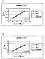
そこで、図2および図3の各図において、水平面と緩斜面との交点にドットを記載する。すると、エッチング途中の形状測定結果に記載された各ドットは、ほぼ一直線上に乗ることがわかる。特に、図3からは、緩斜面の長さが、逆メサ部の外形にかかわらず、逆メサ部の深さにより決定されることがわかる。そこで、図4(1)にエッチング量(逆メサ部の深さ)と緩斜面の長さとの関係を示す。図4(1)により、これらが比例関係にあることが確認できる。したがって、緩斜面のZ′方向長さGは、逆メサ部の深さをDとして、以下の近似式で表すことができる。
【数13】
![]()
一方、図5(1)にエッチング量(逆メサ部の深さ)と急斜面の長さとの関係を示す。これらも比例関係にあるので、急斜面のZ′方向長さHは、以下の近似式で表すことができる。
【数14】
![]()
なお、図4(2)にエッチング量(逆メサ部の深さ)と緩斜面の高さとの関係を示し、図5(2)にエッチング量(逆メサ部の深さ)と急斜面の高さとの関係を示す。図4および図5により、急斜面および緩斜面の長さおよび高さは、エッチング量と比例関係にあることがわかる。また、急斜面および緩斜面の長さおよび高さは、逆メサ部の外形に依存しないことがわかる。以上のことから、主として結晶面に依存するエッチングの異方性により、急斜面および緩斜面が形成されると考えられる。とすれば、エッチングの条件が異なっても、同様の急斜面および緩斜面が形成されると考えられる。
【0029】
上式を利用して、逆メサ型圧電振動片において、各励振電極を平行に配置可能な位置を特定する。図6に励振電極形成位置の説明図を示す。なお図6は、図15のF−F線に相当する部分における正面断面図である。図6では、圧電振動片30の+Y′側に深さDaの逆メサ部10aが形成され、−Y′側に深さDbの逆メサ部10bが形成されている。そして、逆メサ部10aにおける−Z′側端点をRaとし、逆メサ部10bにおける+Z′側端点をRbとしている。ここで、励振電極20を平行に配置することができるのは、逆メサ部10aの水平面12aと逆メサ部10bの水平面12bとがZ′方向において重なり合った平行部分Pである。すなわち、RaのZ′方向位置に、逆メサ部10aの緩斜面16aのZ′方向長さGaを加算した位置以上であり、なおかつ、RbのZ′方向位置から、逆メサ部10bの緩斜面16bのZ′方向長さGbを減算した位置以下である。そして数式13により、Ga=4.0Daであり、Gb=4.0Dbであるから、
【数15】
![]()
【0030】
もっとも、励振電極20の幅Wが、数式15のPの範囲より大きい場合には、励振電極を平行に配置することができない。この場合、逆メサ部の形成位置を変更することにより、平行部分Pの範囲を広げる必要がある。そこで、逆メサ部の形成位置を特定する。
【0031】
図7に逆メサ部を移動させた場合の説明図を示す。図6に対し図7(1)では、矢印11のように、逆メサ部10aを−Z′側に移動させている。図7(1)では、平行部分Pの範囲が励振電極20の幅Wと一致している。すなわち、励振電極20を平行に配置可能となるように、最小限度で逆メサ部10aを移動させた状態である。この場合、圧電振動片の外形を小型化することができる。ここで、逆メサ部10aにおける−Z′側端点Raの位置は、励振電極20における−Z′側端点SaのZ′方向位置から、逆メサ部10aの緩斜面16aのZ′方向長さGa(=4.0Da)を減算した位置である。
【0032】
また、図7(1)に対し図7(2)では、矢印11のように、逆メサ部10aをさらに−Z′側に移動させている。図7(2)では、逆メサ部10aの水平面と逆メサ部10bの水平面とが完全に重なり合い、これ以上逆メサ部10aを−Z′側に移動させると、かえって平行部分Pが減少する。したがって、最大限度まで逆メサ部10aを移動させた状態である。この場合、励振電極の周辺部にも平行部分を確保することが可能となるので、圧電振動片の周波数特性を向上させることができる。ここで、逆メサ部10aにおける−Z′側端点Raの位置は、逆メサ部10bにおける−Z′側端点UbのZ′方向位置に、逆メサ部10bの急斜面14bのZ′方向長さHb(=1.7Db)を加算し、さらに逆メサ部10aの緩斜面16aのZ′方向長さGa(=4.0Da)を減算した位置である。
【0033】
以上により、逆メサ部10aにおける−Z′側端点Raは、次式を満足する位置に形成する。
【数16】
![]()
【数17】
![]()
なお、上記には、逆メサ部を水平移動させて励振電極を平行に配置する場合について述べたが、逆メサ部を拡大することにより励振電極を平行に配置することも可能である。図8に逆メサ部を拡大する場合の説明図を示す。図6に対し図8(1)および(2)はいずれも、逆メサ部10aのみを−Z′方向に拡大したものである。
【0035】
図8(1)では、平行部分Pの範囲が励振電極20の幅Wと一致している。すなわち、励振電極20を平行に配置可能となるように、最小限度で逆メサ部10aを拡大したものである。一方、図8(2)では、逆メサ部10aの水平面と逆メサ部10bの水平面とが完全に重なり合い、これ以上移動させるとかえって平行部分Pは減少する。すなわち、最大限度まで逆メサ部10aを拡大したものである。そしてこの場合にも、逆メサ部10aにおける−Z′側端点Raは、数式16を満足する位置に形成すればよい。なお以上には、+Y′側の逆メサ部10aを拡大する場合を例にして説明したが、−Y′側の逆メサ部10bを拡大する場合も同様に、逆メサ部10bにおける+Z′側端点Rbは、数式17を満足する位置に形成すればよい。
【0036】
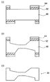
次に、上述した本実施形態に係る逆メサ型ATカット圧電振動片の製造方法について説明する。ここでは代表例として、図7(2)に示す圧電振動片の製造方法について説明する。図9ないし図12に製造工程の説明図を示す。なお、図9および図10では逆メサ部の形成工程を中心に説明するが、現実には圧電基板から圧電振動片をブランクとして形成する工程を同時または順次に行う必要がある。
【0037】
まず、図9(1)に示すように、圧電基板60の表面全体に、耐蝕膜であるAu/Cr膜62を、スパッタ法等により形成する。さらに、Au/Cr膜62の表面全体にポジ型レジスト64を塗布する。
次に、図9(2)に示すように、フォトマスク70a,70bをレジストの上方に配置して、レジスト64を露光する。圧電基板60の+Y′側には、逆メサ部10a(図7(2)参照)に相当する部分に透光部71aを有するフォトマスク70aを配置し、圧電基板60の−Y′側には、逆メサ部10bに相当する部分に透光部71bを有するフォトマスク70bを配置する。なお、ネガ型レジストを使用する場合には、逆メサ部相当部分は遮光部となる。フォトマスク70a,70bには、図15に示す従来の圧電振動片における逆メサ部の形成に使用するフォトマスクを流用することができるので、製造コストを低減することができる。
【0038】
もっとも、本実施形態では、透光部71aにおける−Z′側端点Jaが、透光部71bにおける−Z′側端点Kbより−Z′側に位置するように、フォトマスク70a,70bを配置する。Jaの位置は、図7(2)に示すように、+Y′側励振電極における−Z′側端点SaのZ′方向位置から、逆メサ部10aの緩斜面16aのZ′方向長さGa(=4.0Da)を減算した位置以下とする。なおかつ、逆メサ部10bにおける−Z′側端点UbのZ′方向位置に、逆メサ部10bの急斜面14bのZ′方向長さHb(=1.7Db)を加算し、さらに逆メサ部10aの緩斜面16aのZ′方向長さGa(=4.0Da)を減算した位置以上とする。したがって、
【数18】
![]()
【0039】
および/または、透光部71bにおける+Z′側端点Jbが、透光部71aの+Z′側端点Kaより+Z′側に位置するように、フォトマスク70a,70bを配置する。すなわち、上記と同様の考え方により、
【数19】
![]()
【0040】
なお以上には、逆メサ部の大きさと透光部の大きさとが1:1となる等倍露光の場合について述べている。これ以外の露光倍率(1/5、1/10など)を前提にフォトマスクを形成した場合には、その露光倍率を数式18および数式19の左辺および右辺から除算して、JaおよびJbの位置を決定し、フォトマスク70a,70bを配置する。
そして、上記のように配置したフォトマスク70a,70bを使用して、レジスト64を露光する。次に、図9(3)に示すように、レジスト64を現像して逆メサ部のレジストを除去する。
【0041】
次に、図10(1)に示すように、パターニングされたレジスト64をマスクとして、逆メサ部のAu/Cr膜62をエッチングする。これにより、逆メサ部における圧電基板60が露出することになる。そして、図10(2)に示すように、Au/Cr膜62およびレジスト64をマスクとして、圧電基板60をエッチングする。エッチングはウエットエッチングによって行い、エッチング液にはフッ酸とフッ化アンモニウムとを重量比1:1で混合した液体等を使用する。これにより、圧電基板60の±Y′側が同時にエッチングされる。なお、圧電基板の主振動部が所望の厚さとなるように、時間管理をしつつエッチングを行う。エッチング終了後、レジスト64およびAu/Cr膜62を除去すれば、図10(3)に示すように、圧電振動片の逆メサ部が完成する。
【0042】
次に、圧電振動片の表面に、図15に示す各電極を形成する。まず、図11(1)に示すように、圧電基板60の表面全体に、電極材料であるAu/Cr膜66を、スパッタ法等により形成する。さらに、Au/Cr膜66の表面全体にポジ型レジスト68を塗布する。
【0043】
次に、図11(2)に示すように、圧電基板60の両側におけるレジストの上方にフォトマスク75を配置して、レジスト68を露光する。フォトマスク75は、電極形成部分に相当する部分に、遮光部を有している。なお、ネガ型レジストを使用する場合には、電極相当部分は透光部となる。フォトマスク75には、図15に示す従来の圧電振動片の電極形成に使用するフォトマスクを流用することができるので、製造コストを低減することができる。
【0044】
もっとも、本実施形態では、図7(2)に示すように、逆メサ部10aの水平面と逆メサ部10bの水平面とがZ′方向において重なり合った平行部分Pに、遮光部の励振電極相当部分76が位置するように、フォトマスク75を配置する。平行部分Pは、逆メサ部10aにおける−Z′側端点RaのZ′方向位置に、逆メサ部10aの緩斜面16aのZ′方向長さGa(=4.0Da)を加算した位置以上であって、なおかつ、逆メサ部10bにおける+Z′側端点RbのZ′方向位置から、逆メサ部10bの緩斜面16bのZ′方向長さGb(=4.0Db)を減算した位置以下の範囲である。すなわち、
【数20】
![]()
【0045】
なお以上には、励振電極の大きさと遮光部の大きさとが1:1となる等倍露光の場合について述べている。これ以外の露光倍率(1/5、1/10など)を前提にフォトマスク75を形成した場合には、その露光倍率を数式20の左辺および右辺から除算して、Pの範囲を決定し、フォトマスク75を配置する。
【0046】
そして、上記のように配置したフォトマスク75を使用して、レジスト68を露光する。次に、図11(3)に示すように、レジスト68を現像して、電極形成部分以外の部分のレジストを除去する。
【0047】
次に、図12(1)に示すように、パターニングされたレジスト68をマスクとして、電極形成部分以外の部分のAu/Cr膜66をエッチングする。その後、図12(2)に示すようにレジスト68を除去すれば、圧電基板60の表面に電極が形成される。以上により、圧電振動片が完成する。
【0048】
上記のように形成した本実施形態に係る圧電振動片は、パッケージ内に封入することにより、圧電振動子として使用することができる。図13に圧電振動子の説明図を示す。同図(1)は平面図であり、同図(2)はD−D線における側面断面図である。パッケージ2はセラミック材料等により形成する。また、キャビティ3の底面には電極4及び配線パターン(不図示)を形成して、パッケージ2の底面に形成した外部端子(不図示)との導通を可能とする。そして、圧電振動片30を片持ち状態で実装する。具体的には、電極4の上に導電性接着剤5を塗布し、その上に圧電振動片30の接続電極22を配置して固定する。これにより、パッケージ2の底面の外部端子から、圧電振動片30の励振電極20に通電可能となる。なお、パッケージ2の上部には蓋部材8を装着して、パッケージ2の内部を窒素雰囲気等に保持する。
【0049】
また、本実施形態に係る圧電振動片は、集積回路素子と組み合わせて発振回路を形成することにより、圧電発振器として使用することができる。例えば、図13に示す圧電振動子1と集積回路素子(不図示)とを、配線パターンを形成したモジュール基板上に実装することにより、圧電発振器モジュールを形成することができる。また、図13に示すパッケージ2の内部に、圧電振動片30とともに集積回路素子を封入することにより、圧電発振器パッケージを形成することができる。
【0050】
上述した本実施形態に係る圧電振動片により、励振電極を平行に配置することができる。この点、従来では、逆メサ部に緩斜面が形成されることは知られていなかったので、この緩斜面に励振電極を形成している場合があった。その結果、励振電極が平行に配置されずに、図14(1)のQ部に示すように、不要な振動が多く発生していた。なお、緩斜面に励振電極を形成した場合には、振動部の圧電材料が厚くなっているので、主振動より低い周波数にピークが現れる。
【0051】
なお、特開2001−203449号公報では、図16(1)に示すように、急斜面を外側へ配置する矢印211の方向に、逆メサ部210を水平移動させることにより、図16(2)に示すように、励振電極220を配置する平行部分Pを、広く確保する構造が提案されている。しかし、本発明を前提とすれば、矢印211の方向に逆メサ部を移動させると、励振電極を配置する平行部分がかえって減少することになり、不要な振動を発生させるおそれがある。
【0052】
これに対し、本実施形態に係る逆メサ型ATカット圧電振動片は、特開2001−203449号公報に提案された構造とは逆に、緩斜面を外側へ配置する方向に、逆メサ部210を移動または拡大させる構成とした。これにより、逆メサ型圧電振動片の振動部に平行部分を広く確保することができる。したがって、励振電極を平行に配置することが可能となり、不要な振動を発生させることがない。また、周波数特性に寄与する励振電極の周辺部にも、平行部分を確保することが可能となり、不要な振動を発生させることがない。特に、圧電振動片を小型化する場合には、逆メサ部の水平面が狭くなるので、本実施形態により平行部分を広く確保することが有効である。
【0053】
【発明の効果】
結晶軸(X,Y′,Z′)を有するATカット圧電振動片の、±Y′側主面にそれぞれエッチングにより形成された急斜面、緩斜面および該急斜面、緩斜面との間に水平面を有する逆メサ部を形成し、前記各逆メサ部にそれぞれ励振電極を配置した、逆メサ型ATカット圧電振動片であって、
【数21】
![]()
および/または、
【数22】
![]()
【図面の簡単な説明】
【図1】 逆メサ部に形成される斜面の説明図である。
【図2】 エッチングの進行による逆メサ部の形状変化に関する実験の、各実験サンプルにおける実験結果のグラフであり、(1)はサンプルNo.1の実験結果であり、(2)はサンプルNo.2の実験結果であり、(3)はサンプルNo.3の実験結果である。
【図3】 図2の各図の原点付近の拡大図である。
【図4】 エッチング量と緩斜面の形状との関係を表すグラフであり、(1)は緩斜面の長さとの関係であり、(2)は緩斜面の高さとの関係である。
【図5】 エッチング量と急斜面の形状との関係を表すグラフであり、(1)は急斜面の長さとの関係であり、(2)は急斜面の高さとの関係である。
【図6】 実施形態に係る逆メサ型ATカット圧電振動片の励振電極形成位置の説明図であり、図15のF−F線に相当する部分における正面断面図である。
【図7】 逆メサ部を移動させた場合の説明図であり、(1)は最小限移動させた場合であり、(2)は最大限移動させた場合である。
【図8】 逆メサ部を拡大させた場合の説明図であり、(1)は最小限拡大させた場合であり、(2)は最大限拡大させた場合である。
【図9】 実施形態に係る逆メサ型ATカット圧電振動片の製造方法の工程説明図であり、逆メサ部形成工程の第1説明図である。
【図10】 実施形態に係る逆メサ型ATカット圧電振動片の製造方法の工程説明図であり、逆メサ部形成工程の第2説明図である。
【図11】 実施形態に係る逆メサ型ATカット圧電振動片の製造方法の工程説明図であり、電極形成工程の第1説明図である。
【図12】 実施形態に係る逆メサ型ATカット圧電振動片の製造方法の工程説明図であり、電極形成工程の第2説明図である。
【図13】 圧電振動子の説明図であり、(1)は平面図であり、(2)はD−D線における側面断面図である。
【図14】 逆メサ型ATカット圧電振動片の振動特性図であり、(1)は従来技術に係る圧電振動片であり、(2)は実施形態に係る圧電振動片である。
【図15】 従来技術に係る逆メサ型ATカット圧電振動片の説明図であり、(1)は平面図であり、(2)はF−F線における正面断面図である。
【図16】 特開2001−203449号公報に記載された発明の説明図である。
【符号の説明】
1………圧電振動子、2………パッケージ、3………キャビティ、4………電極、5………導電性接着剤、8………蓋部材、10,10a,10b………逆メサ部、12,12a,12b………水平面、14,14a,14b………急斜面、16,16a,16b………緩斜面、20………励振電極、22………接続電極、30………圧電振動片、60………圧電基板、62………Au/Cr膜、64………レジスト、66………Au/Cr膜、68………レジスト、70,70a,70b………フォトマスク、71a,71b………透光部、75………フォトマスク、76………遮光部、100………圧電振動片、102………振動部、104………周縁部、110………逆メサ部、112………水平面、114………急斜面、115………垂直面、120………励振電極、210………逆メサ部、220………励振電極。[0001]
BACKGROUND OF THE INVENTION
The present invention relates to a piezoelectric vibrating piece, a manufacturing method thereof, and a piezoelectric device.
[0002]
[Prior art]
In order to obtain a constant frequency in an electric circuit, a piezoelectric device on which an AT-cut piezoelectric vibrating piece is mounted is widely used. In general, an AT-cut piezoelectric vibrating piece is formed from a piezoelectric substrate that is cut out along an XZ plane of a piezoelectric material such as quartz that is rotated by a certain angle around the X axis.
[0003]
In recent years, a piezoelectric device having a high resonance frequency has been demanded. In general, the thinner the thickness of the piezoelectric vibrating piece, the higher the resonance frequency of the piezoelectric device. For example, in order to obtain a resonance frequency of 100 MHz or more, the thickness of the piezoelectric vibrating piece needs to be 16 μm or less. However, if the piezoelectric vibrating piece becomes extremely thin, the processing itself becomes difficult, and the rigidity against the impact force becomes weak.
[0004]
Therefore, an inverted mesa type piezoelectric vibrating piece has been proposed. FIG. 15 is an explanatory diagram of an inverted mesa type piezoelectric vibrating piece. FIG. 1A is a plan view, and FIG. 2B is a front sectional view taken along line FF. The inverted mesa type piezoelectric vibrating
[0005]
The reverse mesa portion described above is formed by etching. Here, the piezoelectric material such as quartz has anisotropy in the etching rate depending on the crystal orientation. Therefore, it has been considered that the
[0006]
When the pair of excitation electrodes are not arranged in parallel, many unnecessary vibrations occur, and therefore it is necessary to arrange the excitation electrodes while avoiding the inclined surface of the reverse mesa portion. Therefore, in Japanese Patent Laid-Open No. 2001-203449, by moving the
[0007]
[Problems to be solved by the invention]
However, according to the inventor's experiment, it has been clarified that an inverted mesa portion is formed as shown in FIG. That is, it is confirmed that a
[0008]
If the structure proposed in Japanese Patent Application Laid-Open No. 2001-203449 shown in FIG. 16 is seen on the premise of this, when the reverse mesa portion is moved in the direction of the
[0009]
The present invention pays attention to the above problems, and an object thereof is to provide a piezoelectric vibrating piece and a method for manufacturing the same, in which excitation electrodes can be arranged in parallel and unnecessary vibration is not generated.
Another object of the present invention is to provide a piezoelectric device that does not generate unnecessary vibrations.
[0010]
[Means for Solving the Problems]
In order to achieve the above object, a piezoelectric vibrating piece according to the present invention is a steep slope formed by etching on the ± Y ′ side main surface of an AT-cut piezoelectric vibrating piece having crystal axes (X, Y ′, Z ′). A reverse mesa-type AT-cut piezoelectric vibrating piece in which a reverse mesa portion having a horizontal plane is formed between the gentle slope and the steep slope, the gentle slope, and an excitation electrode is disposed on each reverse mesa portion,
[Expression 7]
![]()
[Equation 8]
![]()
[0011]
Thereby, a wide parallel part can be secured in the vibration part of the inverted mesa type piezoelectric vibrating piece. Therefore, the excitation electrodes can be arranged in parallel, and unnecessary vibrations are not generated.
[0012]
The piezoelectric vibrating piece according to the present invention includes a steep slope, a gentle slope formed by etching on the ± Y ′ side main surface of the AT-cut piezoelectric vibrating piece having crystal axes (X, Y ′, Z ′), and the An inverted mesa type AT-cut piezoelectric vibrating piece in which a reverse mesa part having a horizontal surface is formed between a steep slope and a gentle slope, and an excitation electrode is arranged on each of the reverse mesa parts,
[Equation 9]
![]()
[0013]
In addition, the method for manufacturing a piezoelectric vibrating piece according to the present invention includes an AT cut piezoelectric vibrating piece having crystal axes (X, Y ′, Z ′), a steep slope formed by etching on each ± Y′-side main surface, and a gentle slope. A reverse mesa AT-cut piezoelectric vibrating piece, in which a reverse mesa having a horizontal plane is formed between the slope and the steep slope and the gentle slope, and an excitation electrode is disposed on each reverse mesa, ± Y ′ of the piezoelectric substrate A method for manufacturing an inverted mesa AT-cut piezoelectric vibrating piece, wherein each inverted mesa portion is formed by performing photolithography with a photomask disposed on the side,
[Expression 10]
![]()
[Expression 11]
![]()
As a result, the excitation electrodes can be arranged in parallel, and unnecessary vibrations are not generated.
[0014]
In addition, another method of manufacturing a piezoelectric vibrating piece according to the present invention includes a steep slope formed by etching on each of the ± Y′-side main surfaces of an AT-cut piezoelectric vibrating piece having crystal axes (X, Y ′, Z ′). The reverse mesa-type AT-cut piezoelectric vibrating piece in which a reverse slope mesa part having a horizontal plane is formed between the gentle slope and the steep slope and the gentle slope, and an excitation electrode is disposed on each of the reverse mesa parts. A method of manufacturing an inverted mesa AT-cut piezoelectric vibrating piece, wherein each excitation electrode is formed by performing photolithography with a photomask disposed on the Y ′ side,
[Expression 12]
![]()
[0015]
On the other hand, the piezoelectric device according to the present invention was manufactured using the piezoelectric vibrating piece described above. Thereby, the piezoelectric device which does not generate unnecessary vibration can be provided.
[0016]
DETAILED DESCRIPTION OF THE INVENTION
DESCRIPTION OF EMBODIMENTS Preferred embodiments of a piezoelectric vibrating piece, a manufacturing method thereof, and a piezoelectric device according to the present invention will be described in detail with reference to the accompanying drawings. Note that what is described below is only one aspect of the embodiment of the present invention, and the present invention is not limited thereto.
[0017]
The present invention is based on the knowledge that when the reverse mesa portion of the reverse mesa AT-cut piezoelectric vibrating piece is formed by etching, slopes are formed at both ends in the Z ′ direction of the reverse mesa portion. FIG. 1 is an explanatory view of a slope formed in the reverse mesa portion. In general, piezoelectric materials such as quartz are trigonal and have crystal axes shown in FIG. In the figure, the X axis is an electrical axis, the Y axis is a mechanical axis, and the Z axis is an optical axis. The AT-cut
[0018]
In this AT-cut
[0019]
The experiment was performed by measuring how the shape of the reverse mesa portion in the Z ′ direction changes as the etching of the reverse mesa portion proceeds. In the experiment, an AT-cut quartz crystal vibrating piece having a cut angle of 35 ° 13'30 ″ indicated by θ in FIG. 1 (1) was used. Note that a quartz crystal vibrating piece of any size was used as an experimental sample. The external shape of the inverted mesa portion of the quartz crystal vibrating piece used as an experimental sample is shown in 1. The thickness of each quartz vibrating piece is 0.1 mm (100 μm).
[Table 1]
Etching was performed by wet etching. As the etching solution, a liquid in which hydrofluoric acid and ammonium fluoride were mixed at a weight ratio of 1: 1 was used. On the other hand, the shape measurement of the reverse mesa portion was performed using a non-contact three-dimensional shape measuring apparatus.
[0021]
A specific experimental procedure will be described with reference to FIGS. First, as shown in FIG. 9A, an Au /
[0022]
Next, using the mask formed as described above, the first etching is performed on the inverted mesa portion of the crystal vibrating piece. Here, etching is performed while managing the time so that the depth of the deepest portion of the reverse mesa portion is about 10 μm. Next, using a three-dimensional shape measuring apparatus, the shape of the reverse mesa portion in the Z ′ direction is measured and recorded. Furthermore, the second etching is performed on the same portion, and the shape is measured. Thus, by repeating the etching and the three-dimensional shape measurement four times, it is measured how the shape of the reverse mesa portion in the Z ′ direction changes as the etching progresses. The same experiment as described above is performed for each experimental sample.
[0023]
The experimental results for each experimental sample are shown in FIGS. FIG. 3 is an enlarged view near the origin of FIG. 2 and 3, the horizontal (Z ′) direction distance of the reverse mesa portion is taken on the horizontal axis, and the depth (Y ′) direction distance of the reverse mesa portion is taken on the vertical axis. Further, in each figure, the shape measurement results after the first to fourth etching are shown in an overlapping manner in order from the top. In addition, the origin of the horizontal direction and the depth direction in each shape measurement result was set to the −Z ′ direction end point of the reverse mesa portion. It should be noted that the reverse mesa is slightly expanded in any of the ± Z ′ directions by etching.
[0024]
In FIG. 2, a horizontal plane exists at the center of the inverted mesa portion. In addition, a steep slope exists at the + Z ′ side end of the reverse mesa. Furthermore, a substantially vertical surface exists at the end of the reverse mesa at the −Z ′ side. Each of the above parts has been known to exist. In addition, it can be seen that a gentle slope exists at the corner between the horizontal surface at the center and the vertical surface at the −Z ′ end. Since this gentle slope is much smaller than the steep slope described above, it has been conventionally considered as a part of the horizontal plane described above.
[0025]
And since it is necessary to arrange | position a pair of excitation electrode in a quartz crystal vibrating piece in parallel, it is necessary to arrange | position an excitation electrode on a horizontal surface avoiding this gentle slope. However, as can be seen from FIG. 2, the horizontal length of this gentle slope is very long, and may occupy more than half of the reverse mesa portion due to the progress of etching. In the conventional large-sized inverted mesa type piezoelectric vibrating piece, as a result, a wide horizontal plane could be secured, so the position where the excitation electrode was formed did not become a problem. However, in today where there is a strong demand for miniaturization of the piezoelectric vibrating piece, it is important to know how long the gentle slope is formed in order to arrange the excitation electrode on the horizontal plane. .
[0026]
Therefore, in each of FIGS. 2 and 3, a dot is described at the intersection of the horizontal plane and the gentle slope. Then, it can be seen that the dots described in the shape measurement result during the etching are on a substantially straight line. In particular, it can be seen from FIG. 3 that the length of the gentle slope is determined by the depth of the reverse mesa regardless of the outer shape of the reverse mesa. FIG. 4 (1) shows the relationship between the etching amount (depth of the reverse mesa portion) and the length of the gentle slope. It can be confirmed from FIG. 4A that these are in a proportional relationship. Therefore, the length G of the gentle slope in the Z ′ direction can be expressed by the following approximate expression, where D is the depth of the reverse mesa portion.
[Formula 13]
![]()
On the other hand, FIG. 5A shows the relationship between the etching amount (depth of the reverse mesa portion) and the length of the steep slope. Since these are also in a proportional relationship, the length H of the steep slope in the Z ′ direction can be expressed by the following approximate expression.
[Expression 14]
![]()
4 (2) shows the relationship between the etching amount (depth of the reverse mesa portion) and the height of the gentle slope, and FIG. 5 (2) shows the etching amount (depth of the reverse mesa portion) and the height of the steep slope. The relationship is shown. 4 and 5, it can be seen that the length and height of the steep slope and the gentle slope are proportional to the etching amount. Moreover, it turns out that the length and height of a steep slope and a gentle slope do not depend on the external shape of a reverse mesa part. From the above, it is considered that steep slopes and gentle slopes are formed mainly by etching anisotropy that depends on the crystal plane. If so, it is considered that the same steep slope and gentle slope are formed even if the etching conditions are different.
[0029]
Using the above formula, in the inverted mesa type piezoelectric vibrating piece, a position where each excitation electrode can be arranged in parallel is specified. FIG. 6 is an explanatory diagram of excitation electrode formation positions. FIG. 6 is a front sectional view of a portion corresponding to the line FF in FIG. In FIG. 6, the
[Expression 15]
![]()
[0030]
However, when the width W of the
[0031]
FIG. 7 shows an explanatory diagram when the reverse mesa unit is moved. In FIG. 7A, the
[0032]
Further, in FIG. 7 (2) as compared with FIG. 7 (1), the
[0033]
As described above, the −Z ′ end point Ra in the
[Expression 16]
![]()
[Expression 17]
![]()
In the above description, the case where the reverse mesa portion is horizontally moved and the excitation electrodes are arranged in parallel has been described. However, the excitation electrode may be arranged in parallel by enlarging the reverse mesa portion. FIG. 8 is an explanatory diagram for enlarging the reverse mesa portion. 8 (1) and (2) in FIG. 6 are obtained by enlarging only the
[0035]
In FIG. 8 (1), the range of the parallel portion P coincides with the width W of the
[0036]
Next, a method for manufacturing the inverted mesa AT-cut piezoelectric vibrating piece according to this embodiment described above will be described. Here, as a representative example, a method of manufacturing the piezoelectric vibrating piece shown in FIG. 9 to 12 are explanatory diagrams of the manufacturing process. 9 and 10, the process of forming the reverse mesa portion will be mainly described. However, in reality, the process of forming the piezoelectric vibrating piece from the piezoelectric substrate as a blank needs to be performed simultaneously or sequentially.
[0037]
First, as shown in FIG. 9A, an Au /
Next, as shown in FIG. 9B,
[0038]
However, in the present embodiment, the
[Formula 18]
![]()
[0039]
And / or the
[Equation 19]
![]()
[0040]
In the above description, the case of the same magnification exposure in which the size of the reverse mesa portion and the size of the light transmitting portion is 1: 1 is described. When a photomask is formed on the premise of other exposure magnifications (1/5, 1/10, etc.), the exposure magnification is divided from the left side and the right side of Equations 18 and 19, and the positions of Ja and Jb And
Then, the resist 64 is exposed using the
[0041]
Next, as shown in FIG. 10A, the Au /
[0042]
Next, each electrode shown in FIG. 15 is formed on the surface of the piezoelectric vibrating piece. First, as shown in FIG. 11A, an Au /
[0043]
Next, as shown in FIG. 11B, a
[0044]
However, in this embodiment, as shown in FIG. 7 (2), a portion corresponding to the excitation electrode of the light shielding portion is provided in a parallel portion P where the horizontal plane of the
[Expression 20]
![]()
[0045]
In the above description, the case of the same magnification exposure in which the size of the excitation electrode and the size of the light shielding portion is 1: 1 is described. When the
[0046]
Then, the resist 68 is exposed using the
[0047]
Next, as shown in FIG. 12A, using the patterned resist 68 as a mask, the Au /
[0048]
The piezoelectric vibrating piece according to the present embodiment formed as described above can be used as a piezoelectric vibrator by being enclosed in a package. FIG. 13 is an explanatory diagram of the piezoelectric vibrator. FIG. 1A is a plan view, and FIG. 2B is a side sectional view taken along line DD. The
[0049]
Further, the piezoelectric vibrating piece according to the present embodiment can be used as a piezoelectric oscillator by forming an oscillation circuit in combination with an integrated circuit element. For example, a piezoelectric oscillator module can be formed by mounting the
[0050]
The excitation electrodes can be arranged in parallel by the piezoelectric vibrating piece according to this embodiment described above. In this regard, conventionally, it has not been known that a gentle slope is formed on the reverse mesa portion, and therefore, an excitation electrode may be formed on the gentle slope. As a result, the excitation electrodes were not arranged in parallel, and many unnecessary vibrations occurred as shown in the Q part of FIG. In addition, when the excitation electrode is formed on the gentle slope, the piezoelectric material of the vibration part is thick, and thus a peak appears at a frequency lower than that of the main vibration.
[0051]
In Japanese Patent Application Laid-Open No. 2001-203449, as shown in FIG. 16 (1), by moving the
[0052]
On the other hand, the reverse mesa AT-cut piezoelectric vibrating piece according to the present embodiment has the
[0053]
【The invention's effect】
The AT-cut piezoelectric vibrating piece having crystal axes (X, Y ', Z') has a steep slope, a gentle slope, and a horizontal plane between the steep slope and the gentle slope formed by etching on the main surface of the ± Y 'side. An inverted mesa type AT-cut piezoelectric vibrating piece in which an inverted mesa portion is formed and an excitation electrode is disposed on each of the inverted mesa portions,
[Expression 21]
![]()
And / or
[Expression 22]
![]()
[Brief description of the drawings]
FIG. 1 is an explanatory diagram of a slope formed in a reverse mesa portion.
2 is a graph of experimental results for each experimental sample of an experiment relating to the shape change of the inverted mesa portion due to the progress of etching. (2) is the sample No. 1. (3) is the sample No. 3 shows the experimental results.
FIG. 3 is an enlarged view of the vicinity of the origin of each drawing of FIG. 2;
FIG. 4 is a graph showing the relationship between the etching amount and the shape of a gentle slope, where (1) is the relationship with the length of the gentle slope, and (2) is the relationship with the height of the gentle slope.
FIG. 5 is a graph showing the relationship between the etching amount and the shape of a steep slope, where (1) is the relationship with the length of the steep slope, and (2) is the relationship with the height of the steep slope.
6 is an explanatory diagram of excitation electrode forming positions of the inverted mesa AT-cut piezoelectric vibrating piece according to the embodiment, and is a front sectional view in a portion corresponding to the line FF in FIG. 15;
FIGS. 7A and 7B are explanatory diagrams when the reverse mesa unit is moved. FIG. 7A shows a case where the reverse mesa is moved to the minimum, and FIG. 7B shows a case where the reverse mesa is moved to the maximum.
FIGS. 8A and 8B are explanatory diagrams when the reverse mesa portion is enlarged. FIG. 8A is a case where the reverse mesa portion is enlarged to the minimum, and FIG.
FIG. 9 is a process explanatory diagram of a method for manufacturing an inverted mesa AT-cut piezoelectric vibrating piece according to an embodiment, and is a first explanatory diagram of an inverted mesa part forming process.
FIG. 10 is a process explanatory diagram of a manufacturing method of an inverted mesa AT-cut piezoelectric vibrating piece according to an embodiment, and is a second explanatory diagram of an inverted mesa part forming process.
FIG. 11 is a process explanatory diagram of a method for manufacturing an inverted mesa AT-cut piezoelectric vibrating piece according to an embodiment, and is a first explanatory diagram of an electrode forming process.
FIG. 12 is a process explanatory diagram of a method for manufacturing an inverted mesa AT-cut piezoelectric vibrating piece according to an embodiment, and is a second explanatory diagram of an electrode forming process.
FIG. 13 is an explanatory diagram of a piezoelectric vibrator, (1) is a plan view, and (2) is a side cross-sectional view taken along line DD.
FIG. 14 is a vibration characteristic diagram of an inverted mesa AT-cut piezoelectric vibrating piece, (1) is a piezoelectric vibrating piece according to a conventional technique, and (2) is a piezoelectric vibrating piece according to an embodiment.
FIGS. 15A and 15B are explanatory diagrams of an inverted mesa AT-cut piezoelectric vibrating piece according to the prior art, FIG. 15A is a plan view, and FIG. 15B is a front sectional view taken along line FF.
FIG. 16 is an explanatory diagram of the invention described in Japanese Patent Laid-Open No. 2001-203449.
[Explanation of symbols]
DESCRIPTION OF
Claims (5)
および/または、
前記各励振電極を平行に配置可能としたことを特徴とする圧電振動片。
ただし、Daは+Y′側の前記逆メサ部の深さであり、Dbは−Y′側の前記逆メサ部の深さであり、Saは+Y′側の前記励振電極における−Z′側端点の位置であり、Sbは−Y′側の前記励振電極における+Z′側端点の位置であり、Uaは+Y′側の前記逆メサ部における+Z′側端点の位置であり、Ubは−Y′側の前記逆メサ部における−Z′側端点の位置である。The AT-cut piezoelectric vibrating piece having crystal axes (X, Y ', Z') has a steep slope, a gentle slope, and a horizontal plane between the steep slope and the gentle slope formed by etching on the main surface of the ± Y 'side. An inverted mesa type AT-cut piezoelectric vibrating piece in which an inverted mesa portion is formed and an excitation electrode is disposed on each of the inverted mesa portions,
And / or
A piezoelectric vibrating piece characterized in that the excitation electrodes can be arranged in parallel.
Where Da is the depth of the reverse mesa on the + Y ′ side, Db is the depth of the reverse mesa on the −Y ′ side, and Sa is the −Z ′ end point of the excitation electrode on the + Y ′ side. Sb is the position of the + Z ′ side end point of the excitation electrode on the −Y ′ side, Ua is the position of the + Z ′ side end point of the reverse mesa portion on the + Y ′ side, and Ub is −Y ′. This is the position of the −Z ′ side end point in the reverse mesa portion on the side.
前記各励振電極を平行に配置可能としたことを特徴とする圧電振動片。
ただし、Daは+Y′側の前記逆メサ部の深さであり、Dbは−Y′側の前記逆メサ部の深さであり、Raは+Y′側の前記逆メサ部における−Z′側端点の位置であり、Rbは−Y′側の前記逆メサ部における+Z′側端点の位置である。The AT-cut piezoelectric vibrating piece having crystal axes (X, Y ', Z') has a steep slope, a gentle slope, and a horizontal plane between the steep slope and the gentle slope formed by etching on the main surface of the ± Y 'side. An inverted mesa type AT-cut piezoelectric vibrating piece in which an inverted mesa portion is formed and an excitation electrode is disposed on each of the inverted mesa portions,
A piezoelectric vibrating piece characterized in that the excitation electrodes can be arranged in parallel.
Where Da is the depth of the reverse mesa portion on the + Y ′ side, Db is the depth of the reverse mesa portion on the −Y ′ side, and Ra is the −Z ′ side in the reverse mesa portion on the + Y ′ side. It is the position of the end point, and Rb is the position of the + Z ′ side end point in the reverse mesa portion on the −Y ′ side.
圧電基板の±Y′側にフォトマスクを配置してフォトリソグラフィを行うことにより、前記各逆メサ部を形成する、逆メサ型ATカット圧電振動片の製造方法であって、
および/または、
前記各励振電極を平行に配置可能とすることを特徴とする圧電振動片の製造方法。
ただし、Cは露光倍率であり、Daは+Y′側の前記逆メサ部の深さであり、Dbは−Y′側の前記逆メサ部の深さであり、Saは+Y′側の前記励振電極における−Z′側端点の位置であり、Sbは−Y′側の前記励振電極における+Z′側端点の位置であり、Uaは+Y′側の前記逆メサ部における+Z′側端点の位置であり、Ubは−Y′側の前記逆メサ部における−Z′側端点の位置である。The AT-cut piezoelectric vibrating piece having crystal axes (X, Y ', Z') has a steep slope, a gentle slope, and a horizontal plane between the steep slope and the gentle slope formed by etching on the main surface of the ± Y 'side. For the inverted mesa type AT-cut piezoelectric vibrating piece in which the inverted mesa part is formed and the excitation electrode is arranged on each of the inverted mesa parts,
A method of manufacturing an inverted mesa AT-cut piezoelectric vibrating piece, wherein each of the inverted mesa parts is formed by performing photolithography by arranging a photomask on the ± Y ′ side of the piezoelectric substrate,
And / or
A method of manufacturing a piezoelectric vibrating piece, wherein the excitation electrodes can be arranged in parallel.
Where C is the exposure magnification, Da is the depth of the reverse mesa on the + Y ′ side, Db is the depth of the reverse mesa on the −Y ′ side, and Sa is the excitation on the + Y ′ side. -B 'is the position of the -Z' side end point of the electrode, Sb is the position of the + Z 'side end point of the excitation electrode on the -Y' side, and Ua is the position of the + Z 'side end point of the reverse mesa on the + Y' side. Yes, Ub is the position of the -Z 'end point in the reverse mesa on the -Y' side.
圧電基板の±Y′側にフォトマスクを配置してフォトリソグラフィを行うことにより、前記各励振電極を形成する、逆メサ型ATカット圧電振動片の製造方法であって、
前記各励振電極を平行に配置可能とすることを特徴とする圧電振動片の製造方法。
ただし、Cは露光倍率であり、Daは+Y′側の前記逆メサ部の深さであり、Dbは−Y′側の前記逆メサ部の深さであり、Raは+Y′側逆メサ部の−Z′側端点の位置であり、Rbは−Y′側逆メサ部の+Z′側端点の位置である。The AT-cut piezoelectric vibrating piece having crystal axes (X, Y ', Z') has a steep slope, a gentle slope, and a horizontal plane between the steep slope and the gentle slope formed by etching on the main surface of the ± Y 'side. For the inverted mesa type AT-cut piezoelectric vibrating piece in which the inverted mesa part is formed and the excitation electrode is arranged on each of the inverted mesa parts,
A method for producing an inverted mesa AT-cut piezoelectric vibrating piece, wherein each excitation electrode is formed by performing photolithography with a photomask disposed on the ± Y ′ side of a piezoelectric substrate,
A method of manufacturing a piezoelectric vibrating piece, wherein the excitation electrodes can be arranged in parallel.
Where C is the exposure magnification, Da is the depth of the reverse mesa portion on the + Y ′ side, Db is the depth of the reverse mesa portion on the −Y ′ side, and Ra is the reverse mesa portion on the + Y ′ side. -Z 'side end point, and Rb is the position of the + Z' side end point of the -Y 'side reverse mesa.
Priority Applications (1)
| Application Number | Priority Date | Filing Date | Title |
|---|---|---|---|
| JP2002065875A JP3952811B2 (en) | 2002-03-11 | 2002-03-11 | Piezoelectric vibrating piece, method for manufacturing piezoelectric vibrating piece, and piezoelectric device |
Applications Claiming Priority (1)
| Application Number | Priority Date | Filing Date | Title |
|---|---|---|---|
| JP2002065875A JP3952811B2 (en) | 2002-03-11 | 2002-03-11 | Piezoelectric vibrating piece, method for manufacturing piezoelectric vibrating piece, and piezoelectric device |
Publications (2)
| Publication Number | Publication Date |
|---|---|
| JP2003264446A JP2003264446A (en) | 2003-09-19 |
| JP3952811B2 true JP3952811B2 (en) | 2007-08-01 |
Family
ID=29197966
Family Applications (1)
| Application Number | Title | Priority Date | Filing Date |
|---|---|---|---|
| JP2002065875A Expired - Fee Related JP3952811B2 (en) | 2002-03-11 | 2002-03-11 | Piezoelectric vibrating piece, method for manufacturing piezoelectric vibrating piece, and piezoelectric device |
Country Status (1)
| Country | Link |
|---|---|
| JP (1) | JP3952811B2 (en) |
Families Citing this family (12)
| Publication number | Priority date | Publication date | Assignee | Title |
|---|---|---|---|---|
| JP5534217B2 (en) * | 2010-11-10 | 2014-06-25 | セイコーエプソン株式会社 | Piezoelectric substrate, method for manufacturing the same, and method for manufacturing a piezoelectric vibrating piece |
| TW201251157A (en) | 2011-06-03 | 2012-12-16 | Seiko Epson Corp | Piezoelectric vibration element, manufacturing method for piezoelectric vibration element, piezoelectric vibrator, electronic device, and electronic apparatus |
| CN102957394B (en) | 2011-08-18 | 2016-12-21 | 精工爱普生株式会社 | The manufacture method of vibrating elements, oscillator, electronic installation, electronic equipment, moving body and vibrating elements |
| US8970316B2 (en) | 2011-08-19 | 2015-03-03 | Seiko Epson Corporation | Resonating element, resonator, electronic device, electronic apparatus, and mobile object |
| JP6051885B2 (en) | 2013-01-18 | 2016-12-27 | セイコーエプソン株式会社 | Vibration element, vibrator, oscillator, electronic device, and moving object |
| JP6472941B2 (en) * | 2013-01-18 | 2019-02-20 | セイコーエプソン株式会社 | AT-cut quartz substrate processing method and vibration element manufacturing method |
| JP6390104B2 (en) | 2013-03-05 | 2018-09-19 | セイコーエプソン株式会社 | Vibration element, vibrator, oscillator, electronic device, and moving object |
| JP6107330B2 (en) | 2013-03-29 | 2017-04-05 | セイコーエプソン株式会社 | Vibration element, vibrator, oscillator, electronic device, and moving object |
| JP6498379B2 (en) | 2013-03-29 | 2019-04-10 | セイコーエプソン株式会社 | Vibration element, vibrator, oscillator, electronic device, and moving object |
| JP6435606B2 (en) | 2013-03-29 | 2018-12-12 | セイコーエプソン株式会社 | Vibration element, vibrator, oscillator, electronic device, and moving object |
| JP6410117B2 (en) * | 2017-02-21 | 2018-10-24 | エスアイアイ・クリスタルテクノロジー株式会社 | Method for manufacturing quartz vibrating piece |
| JP7256680B2 (en) * | 2019-04-24 | 2023-04-12 | 京セラ株式会社 | Piezoelectric piece for vibration element, piezoelectric vibration element and piezoelectric device |
-
2002
- 2002-03-11 JP JP2002065875A patent/JP3952811B2/en not_active Expired - Fee Related
Also Published As
| Publication number | Publication date |
|---|---|
| JP2003264446A (en) | 2003-09-19 |
Similar Documents
| Publication | Publication Date | Title |
|---|---|---|
| JP4714770B2 (en) | Tuning fork type piezoelectric vibrating piece and method for manufacturing tuning fork type piezoelectric vibrating piece | |
| JP3952811B2 (en) | Piezoelectric vibrating piece, method for manufacturing piezoelectric vibrating piece, and piezoelectric device | |
| JP5059399B2 (en) | Method for manufacturing piezoelectric vibrating piece, piezoelectric vibrating piece and piezoelectric device | |
| JP4593203B2 (en) | Tuning fork crystal unit and method for manufacturing the same | |
| JPH1041772A (en) | Manufacture of crystal vibrator | |
| JP3844213B2 (en) | Method for manufacturing piezoelectric vibrating piece, photomask, piezoelectric vibrating piece, and piezoelectric device | |
| US10862453B2 (en) | Crystal oscillating element, crystal oscillation device, and method of manufacturing crystal oscillating element | |
| JP5088664B2 (en) | Method for manufacturing piezoelectric vibrating piece | |
| JP5384406B2 (en) | Manufacturing method of tuning-fork type crystal vibrating piece, crystal device | |
| JP2007329879A (en) | Tuning-fork type bending crystal oscillator piece and manufacturing method therefor | |
| JP2011217041A (en) | Method for manufacturing tuning fork type crystal piece | |
| JP2009152988A (en) | Piezoelectric vibration chip, piezoelectric device and manufacturing methods for them | |
| JP2018125656A (en) | Tuning fork type vibrator | |
| JP5171551B2 (en) | Tuning fork type crystal resonator element frequency adjustment method | |
| JP2004120351A (en) | Manufacturing method of piezoelectric vibration piece | |
| JP2008113380A (en) | Method for manufacturing crystal vibrator, crystal vibrator, and electronic component | |
| JP2005020141A (en) | Manufacturing method of piezoelectric vibration chip and manufacturing method of piezoelectric device | |
| JP2011217039A (en) | Method of manufacturing tuning fork type quartz piece | |
| JP2004301552A (en) | Vibrator and physical quantity measuring apparatus | |
| CN112787619A (en) | Piezoelectric element and method for manufacturing the same | |
| JP5534217B2 (en) | Piezoelectric substrate, method for manufacturing the same, and method for manufacturing a piezoelectric vibrating piece | |
| JP2017085341A5 (en) | ||
| JP6611534B2 (en) | Piezoelectric vibrator element and piezoelectric vibrator | |
| JP5908630B2 (en) | Piezoelectric vibrating piece, piezoelectric vibrator, and method of manufacturing piezoelectric vibrating piece | |
| JP7423231B2 (en) | Manufacturing method of piezoelectric vibrating piece, piezoelectric vibrating piece and piezoelectric vibrator |
Legal Events
| Date | Code | Title | Description |
|---|---|---|---|
| A621 | Written request for application examination |
Free format text: JAPANESE INTERMEDIATE CODE: A621 Effective date: 20040430 |
|
| A977 | Report on retrieval |
Free format text: JAPANESE INTERMEDIATE CODE: A971007 Effective date: 20051221 |
|
| A131 | Notification of reasons for refusal |
Free format text: JAPANESE INTERMEDIATE CODE: A131 Effective date: 20060516 |
|
| A521 | Request for written amendment filed |
Free format text: JAPANESE INTERMEDIATE CODE: A523 Effective date: 20060629 |
|
| A02 | Decision of refusal |
Free format text: JAPANESE INTERMEDIATE CODE: A02 Effective date: 20061226 |
|
| A521 | Request for written amendment filed |
Free format text: JAPANESE INTERMEDIATE CODE: A523 Effective date: 20070118 |
|
| A911 | Transfer to examiner for re-examination before appeal (zenchi) |
Free format text: JAPANESE INTERMEDIATE CODE: A911 Effective date: 20070323 |
|
| TRDD | Decision of grant or rejection written | ||
| A01 | Written decision to grant a patent or to grant a registration (utility model) |
Free format text: JAPANESE INTERMEDIATE CODE: A01 Effective date: 20070410 |
|
| A61 | First payment of annual fees (during grant procedure) |
Free format text: JAPANESE INTERMEDIATE CODE: A61 Effective date: 20070423 |
|
| R150 | Certificate of patent or registration of utility model |
Free format text: JAPANESE INTERMEDIATE CODE: R150 |
|
| FPAY | Renewal fee payment (event date is renewal date of database) |
Free format text: PAYMENT UNTIL: 20110511 Year of fee payment: 4 |
|
| FPAY | Renewal fee payment (event date is renewal date of database) |
Free format text: PAYMENT UNTIL: 20120511 Year of fee payment: 5 |
|
| FPAY | Renewal fee payment (event date is renewal date of database) |
Free format text: PAYMENT UNTIL: 20120511 Year of fee payment: 5 |
|
| FPAY | Renewal fee payment (event date is renewal date of database) |
Free format text: PAYMENT UNTIL: 20130511 Year of fee payment: 6 |
|
| FPAY | Renewal fee payment (event date is renewal date of database) |
Free format text: PAYMENT UNTIL: 20140511 Year of fee payment: 7 |
|
| S531 | Written request for registration of change of domicile |
Free format text: JAPANESE INTERMEDIATE CODE: R313531 |
|
| R350 | Written notification of registration of transfer |
Free format text: JAPANESE INTERMEDIATE CODE: R350 |
|
| LAPS | Cancellation because of no payment of annual fees |