JP2004120351A - Manufacturing method of piezoelectric vibration piece - Google Patents
Manufacturing method of piezoelectric vibration piece Download PDFInfo
- Publication number
- JP2004120351A JP2004120351A JP2002280909A JP2002280909A JP2004120351A JP 2004120351 A JP2004120351 A JP 2004120351A JP 2002280909 A JP2002280909 A JP 2002280909A JP 2002280909 A JP2002280909 A JP 2002280909A JP 2004120351 A JP2004120351 A JP 2004120351A
- Authority
- JP
- Japan
- Prior art keywords
- wafer
- corrosion
- resistant film
- forming
- exposed
- Prior art date
- Legal status (The legal status is an assumption and is not a legal conclusion. Google has not performed a legal analysis and makes no representation as to the accuracy of the status listed.)
- Granted
Links
Images


Abstract
Description
【0001】
【発明の属する技術分野】
本発明は、エッチング異方性を有す根水晶等の圧電材料からになるウエハをフォトエッチングしかつその表面に電極膜をパターニングして圧電振動片を製造する方法に関し、特に、圧電振動ジャイロのような音叉型圧電振動片の振動腕の側面に、その厚み方向に分離された電極を形成する方法に関する。
【0002】
【従来の技術】
従来より、船舶・航空機・自動車等の姿勢制御や航行制御、ビデオカメラ等の手振れ防止・検出等における回転角速度センサとして、圧電振動ジャイロが広く利用されており、3次元立体マウス等の回転方向センサにも応用されている。図5は、このような圧電振動ジャイロに使用するための音叉型水晶振動片の一例を示している。音叉型水晶振動片1は、図5(A)に示すように、中央の基部2から一方の側に延出する1対の駆動用振動腕3と、それとは反対側に延出する1対の検出用振動腕4とを有する。音叉型水晶振動片1は、基部2から突出する支持部2a、2bを接着固定して所定のパッケージ内にマウントされ、圧電振動ジャイロを構成する。(例えば、下記特許文献1を参照。)
【0003】
検出用振動腕4には、図5(B)に示すように、その側面にそれぞれ厚み方向に分離された2対の検出用電極5a、5bが設けられている。駆動用振動腕3には、図5(C)に示すように、その上下主面に形成された長手方向の溝6の内面に第1の駆動用電極7a、7bが設けられ、かつその側面に第2の駆動用電極8a、8bが設けられ、互いに電気的に接続されて音叉型水晶振動片1を振動させる駆動電極を構成している。前記駆動電極に所定の交流電圧を印加すると、隣接する第1及び第2の駆動用電極7a、8a及び7b、8b間で電界が交互に発生して、その共振周波数で駆動用振動腕3が屈曲振動する。このように第1の駆動用電極7a、7bが溝6の内面に設けられた構成では、前記電界が前記各主面に平行に発生するので、電界効率が大幅に向上し、CI値を低く抑制することができる。
【0004】
この状態で音叉型水晶振動片1が図5(A)のY軸9を中心に回転すると、その回転角速度に対して、その振動方向と直交する向きに働くコリオリ力により、駆動用振動腕3は垂直方向に応力を受け、垂直方向に振動する。この振動が基部2を介して伝達されて、検出用振動腕4をその共振周波数で振動させる。これを電気信号として検出用電極5a、5bから検出することにより、音叉型水晶振動片1の回転角速度及びその回転方向等が求められる。
【0005】
従来、音叉型水晶振動片1は、フォトリソグラフィ技術を利用して水晶ウエハをウエットエッチングすることにより所望の外形及び各振動腕の溝を加工し、かつその表面にスパッタリング等で被着させた電極膜をパターニングして所望の電極や電極パッド及びそれらを接続する配線パターンを形成する。検出用電極5a、5bは、水晶ウエハが或る程度の厚みを有する場合には、検出用振動腕4の側面全面に電極膜を成膜した後、その厚み方向中央の不要部分を機械的又は化学的に剥離することによって形成できる。しかしながら最近は、電子機器の小型化に伴い圧電デバイスが小型化・薄型化されて、ウエハが非常に薄くなっているので、このような方法で電極膜を分離させることは困難である。
【0006】
圧電デバイスの小型化・薄型化に対応するために、下記特許文献1には、水晶板に振動子の外形を両面から、その厚みを一部残すようにエッチングして溝を形成しかつその側面に電極膜を形成した後、該溝のエッチング残りの部分を機械的に折って、個々の振動子を分離させると同時に、その際に溝に残存する突起によって厚み方向に分離させた電極を形成する方法が記載されている。更に下記特許文献2には、前記溝のエッチング残りの部分をエッチングで除去することにより、同様に電極を厚み方向に分割させる方法が開示されている。
【0007】
【特許文献1】特開平8−18371号公報
【特許文献2】特開平8−162874号公報
【0008】
【発明が解決しようとする課題】
しかしながら、上記特許文献1に記載される方法では、溝のエッチング残りの部分を折る際に、水晶の破片が生じて水晶振動子に付着し、その振動特性を変化させたり、隣接する水晶振動子や治具と接触して電極膜を損傷し、不良品の発生及び歩留まりの低下を招く虞がある。更に、折る位置を正確に制御できないので、水晶振動子の側面に残存する突起の大きさが均一にならず、振動腕のバランスを損なって不要な振動を発生させ、振動特性を低下させるという問題が生じる。
また、エッチング残りの部分で水晶振動子を折るためには、特殊な治具が必要で、そのために作業が複雑化しかつ製造コストを増大させる結果となる。
【0009】
また、上記特許文献2の方法では、エッチングでエッチング残りの部分を完全に除去する際に、水晶の結晶異方性のために、水晶振動子の側面がオーバエッチングされて凹みが形成される虞がある。更に、エッチング残りの部分に形成したレジスト膜を剥離することにより、その上に後から形成された電極膜をリフトオフしているが、このとき除去された電極材料が電極に再付着する虞がある。
【0010】
そこで本発明は、上述した従来の問題点に鑑みてなされたものであり、その目的は、フォトリソグラフィ技術を利用した従来の加工工程を用いて、複雑な工程を追加したり特別な工具や設備を用いる必要が無く、電極を損傷したり振動特性に影響を与えることなく、簡単にかつ低コストで、圧電振動片側面の厚み方向に分離した電極を有する圧電振動片を製造し得る方法を提供することにある。
【0011】
【課題を解決するための手段】
本発明によれば、上記目的を達成するために、厚み方向により高いエッチングレートを有する圧電材料からなるウエハの両主面に耐蝕膜を形成する工程と、振動片の外形及びその外側に拡大した余白部分を含む予備形状を前記耐蝕膜にパターニングして、前記ウエハの表面を露出させる工程と、前記耐蝕膜の上にフォトレジスト層を形成して前記振動片外形をパターニングし、前記余白部分に対応する前記耐蝕膜の部分を露出させる工程と、前記ウエハの露出面を貫通エッチングして、前記予備形状を形成する工程と、前記余白部分に対応する前記耐蝕膜の露出部分を除去して、前記ウエハの表面を露出させる工程と、前記予備形状の側面にその厚み方向中央に突条を残すように前記ウエハの露出面をエッチングして、前記振動片外形を形成する工程と、残存する前記フォトレジスト層及び前記耐蝕膜を除去した後、前記突条を含む前記振動片側面に電極膜を形成しかつパターニングして、前記突条の先端に前記圧電材料の表面を露出させる工程と、残存する前記フォトレジスト層を除去する工程とを含むことを特徴とする圧電振動片の製造方法が提供される。
【0012】
前記ウエハは、厚み方向により高いエッチングレートを有するので、振動片外形を形成するためにウエハ露出面をエッチングする際に、ウエハはその幅方向よりも厚み方向により速くエッチングされるから、耐蝕膜のパターニングで加工範囲を限定しつつ、加工時間等の条件を調整することによって、振動片自体が小型化されても、振動片側面の厚み方向中央に突条を形成することは容易である。このように圧電材料のエッチング異方性を利用してウエハの厚み方向と幅方向とでエッチング速度を制御することにより、振動片の特性に影響を与えない程度の高さを有する突条を側面に形成し、該側面に形成される電極を従来のフォトリソグラフィ技術を利用したエッチング工程により、厚み方向に分離させることができる。従って、複雑な工程を追加したり特別な工具や設備を用いる必要が無く低コストであり、加工時に電極を損傷したり異物の付着により振動特性に影響を与えることなく、所望の圧電振動片を歩留まり良く製造することができる。
【0013】
圧電材料としては、従来から一般に採用されている水晶が好ましく、その結晶異方性からウエハの厚み方向を水晶のZ軸方向に対応して配向するのが好ましい。
【0014】
或る実施例において、ウエハ側面に形成した電極膜のパターニングは、フォトリソグラフィ技術を利用して、前記電極膜の上にフォトレジスト層を形成しかつパターニングして前記突条の先端に電極膜を露出させ、この電極膜の露出部分を除去して突条の先端に圧電材料の表面を露出させることにより、簡単に加工することができる。
【0015】
本発明の別の側面によれば、厚み方向により高いエッチングレートを有する圧電材料からなるウエハの両主面に耐蝕膜を形成する工程と、1対の振動腕を有する音叉型振動片の外形及び前記振動腕の外側に拡大した余白部分を含む予備形状を前記耐蝕膜にパターニングして、前記ウエハの表面を露出させる工程と、前記耐蝕膜の上にフォトレジスト層を形成して前記振動片外形をパターニングし、前記余白部分に対応する前記耐蝕膜の部分を露出させる工程と、前記ウエハの露出面を貫通エッチングして、前記予備形状を形成する工程と、前記余白部分に対応する前記耐蝕膜の露出部分を除去して、前記予備形状の表面を露出させる工程と、前記ウエハの側面にその厚み方向中央に突条を残すように前記ウエハの露出面をエッチングして、前記振動片外形を形成する工程と、残存する前記フォトレジスト層及び前記耐蝕膜を除去した後、前記突条を含む前記振動片側面に電極膜を形成しかつパターニングして、前記突条の先端に前記圧電材料の表面を露出させる工程と、残存する前記フォトレジスト層を除去する工程とを含むことを特徴とする圧電振動片の製造方法が提供される。
【0016】
同様に、圧電材料としては、従来から一般に採用されている水晶が好ましく、その結晶異方性から振動腕の長手方向、幅方向及び厚み方向をそれぞれ水晶のY軸方向、X軸方向及びZ軸方向に対応して配向するのが好ましい。
【0017】
また、前記ウエハ側面に形成した電極膜のパターニングは、同様に前記電極膜の上にフォトレジスト層を形成しかつパターニングして前記突条の先端に電極膜を露出させ、この電極膜の露出部分を除去して突条の先端に圧電材料の表面を露出させることにより、簡単に加工することができる。
【0018】
或る実施例では、前記音叉型振動片が前記1対の振動腕とは逆向きに延出する別の1対の振動腕を有し、前記予備形状が前記別の1対の振動腕の外側には拡大した余白部分を含まないように形成され、振動片側面に電極膜を形成しかつパターニングする前記工程において、それと同時に、前記別の1対の振動腕の全表面に電極膜を形成しかつパターニングする。これにより、図5に関連して上述した圧電ジャイロセンサのような音叉型圧電振動片の2対の振動腕を、工数を増やすことなく同時に加工することができる。
【0019】
別の実施例では、更に前記音叉型振動片が前記別の1対の振動腕の主面にその内面に駆動用電極が形成される長手方向の溝を有し、耐蝕膜上にフォトレジスト層を形成して振動片外形をパターニングする前記工程において、余白部分に対応する耐蝕膜の部分を露出させると同時に、前記溝に対応する耐蝕膜の部分を露出させ、余白部分に対応する耐蝕膜の露出部分を除去する前記工程において、それと同時に、前記溝に対応する耐蝕膜の露出部分を除去してウエハの表面を露出させ、ウエハ露出面をエッチングする前記工程において、振動片側面の厚み方向中央に突条を残すと同時に、前記別の1対の振動腕の主面に前記溝を形成する。これにより、振動腕の溝の内面に電極を設けて電界効率が大幅に向上させかつCI値を低く抑制した構成の圧電振動片を、その製造工程をそのまま利用して、工数を増やすことなく製造することができる。
【0020】
【発明の実施の形態】
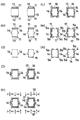
図1〜図4は、本発明の方法を適用して、図5に示す圧電振動ジャイロ用音叉型水晶振動片1を製造する過程を示しており、特に図1及び図2は検出用振動腕4の断面を、図3及び図4は駆動用振動腕3の断面をそれぞれ示している。先ず、図1(A)、図3(A)に示すように、本実施例において水晶である圧電材料のウエハ10の両面に耐蝕膜11を全面に形成し、かつその上にフォトレジスト層12をスピンコートによりウエハ全面に形成する。耐蝕膜11は、一般にウエハのエッチング液に対して十分な耐蝕性を有する金属材料で形成され、本実施例では、それぞれスパッタリング又は蒸着でウエハ表面に積層したCr/Au膜を使用する。
【0021】
次に、第1フォトマスクを用いてフォトレジスト層12をパターニングし、それにより露出した耐蝕膜11をエッチングにより図1(B)、図3(B)のように除去して、ウエハ10表面を露出させる。前記第1フォトマスクは、振動片1の外形及びその検出用振動腕4の外側に拡大した余白部分を含む予備形状のマスクパターンを有する。但し、この予備形状は、駆動用振動腕3の外側には余白部分を設けない。このとき、前記第1フォトマスクはウエハ10に対して、水晶の結晶異方性を考慮して、前記各振動腕の長手方向、幅方向及び厚み方向がそれぞれ水晶のY軸方向、X軸方向及びZ軸方向に対応するように配向する。
【0022】
図1(C)及び(D)、図3(C)及び(D)に示すように、残存するフォトレジスト層12を完全に除去した後、新たにフォトレジスト層13をスピンコートによりウエハ全面に形成する。フォトレジスト層13は、振動片1の外形及び駆動用振動腕3の溝6に対応するマスクパターンの第2フォトマスクを用いてパターニングする。これにより、検出用振動腕については、図1(E)に示すように前記余白部分に対応する耐蝕膜11の部分及びウエハ10表面が露出する。駆動用振動腕については、図3(E)に示すように前記溝に対応する耐蝕膜11の部分及びウエハ10表面が露出する。
【0023】
次に、ウエハ10の露出面を弗酸(HF)等の適当なエッチング液で貫通エッチングする。これにより、検出用振動腕については、図1(F)に示すように前記余白部分を含む前記予備形状の外形を、駆動用振動腕については、図3(F)に示すように所望の外形を形成する。図1(F)及び図3(F)の耐蝕膜11の各露出部分は、それぞれエッチングにより除去する。これにより、検出用振動腕については、図2(G)に示すように前記余白部分に対応するウエハ10の表面が露出し、駆動用振動腕については、図4(G)に示すように溝6に対応するウエハ10の表面が露出する。
【0024】
次に、ウエハ10の露出面を適当なエッチング液でエッチングする。検出用振動腕については、図2(H)に示すように前記余白部分が削除され、かつその側面の厚み方向中央に突条14が残るように加工する。これと同時に、駆動用振動腕については、図4(H)に示すように溝6が上下主面に形成される。上述したように前記各振動腕の長手方向、幅方向及び厚み方向をそれぞれ水晶のY軸方向、X軸方向及びZ軸方向に対応させて配向し、厚み方向のエッチングレートが幅方向よりも高くなるようにしたので、エッチング時間等の加工条件を適当に制御することによって、水晶振動片1の振動特性に実質的な影響を与えない程度の突条14を容易に形成することができる。
【0025】
残存するフォトレジスト層13及び耐蝕膜11を完全に除去すると、図2(I)、図4(I)のように所望の外形及び表面形状を有する水晶素子片15が完成する。次に、図2(J)、図4(J)に示すように、溝6の内面を含む水晶素子片15の全表面に、Cr/Au膜からなる電極膜16を形成しかつその上にフォトレジスト層17を形成する。
【0026】
フォトレジスト層17は、電極膜16を所望の電極パターンに形成するために、第3フォトマスク18を用いてパターニングする。検出用振動腕については、図2(K)に示すようにフォトレジスト層17の突条14先端に形成した部分と上下主面の中央部分とを露光しかつ現像して、図2(L)に示すようにこれらの部分に電極膜16を露出させる。同時に、駆動用振動腕については、図4(L)に示すように上下主面の溝6の両側をパターニングして、電極膜16を露出させる。
【0027】
次に、電極膜16の露出部分を適当なエッチング液で除去して、ウエハ表面を露出させる。これにより、検出用振動腕については、図2(M)に示すように、その側面に厚み方向の中央で突条14により分離された所望の検出用電極5a・5bが形成される。同時に、駆動用振動腕については、図4(M)に示すように溝6の内面と側面とに分離された駆動用電極7a・7bが得られる。最後に、残存するフォトレジスト層17を除去することにより、図5の音叉型水晶振動片1が完成する。
【0028】
以上、本発明の好適な実施例について詳細に説明したが、本発明はその技術的範囲において上記実施例に様々な変形・変更を加えて実施することができる。例えば、上記実施例ではウエハの表面をウェットエッチングにより加工したが、ドライエッチングを用いることもできる。また、上記実施例では、圧電振動ジャイロ用の圧電振動子について、その検出用電極を形成する過程を説明したが、本発明は、その側面に厚み方向に分離した電極を有する様々な圧電振動片の製造に適用することができる。
【図面の簡単な説明】
【図1】本発明の方法を適用して圧電振動ジャイロ用音叉型水晶振動片を製造する過程を、図5のB−B断面において工程順に示す(A)〜(F)図からなる断面図。
【図2】図1に続く過程を工程順に示す(G)〜(N)図からなる同様の断面図。
【図3】図1に対応する過程を、図5のC−C断面において工程順に示す(A)〜(F)図からなる断面図。
【図4】図3に続く過程を工程順に示す(G)〜(N)図からなる同様の断面図。
【図5】(A)図は圧電振動ジャイロ用音叉型水晶振動片の平面図、(B)図はそのB−B線における検出用振動腕の断面図、(C)図はそのC−C線における駆動用振動腕の断面図である。
【符号の説明】
1 音叉型水晶振動片、2 基部、2a・2b 支持部、3 駆動用振動腕、4検出用振動腕、5a・5b 検出用電極、6 溝、7a・7b 第1の駆動用電極、8a・8b 第2の駆動用電極、9 Y軸、10 ウエハ、11 耐蝕膜、12・13 フォトレジスト層、14 突条、15 水晶素子片、16 電極膜、17 フォトレジスト層、18 第3フォトマスク[0001]
TECHNICAL FIELD OF THE INVENTION
The present invention relates to a method for manufacturing a piezoelectric vibrating reed by photoetching a wafer made of a piezoelectric material such as a root quartz having etching anisotropy and patterning an electrode film on the surface thereof. The present invention relates to a method of forming electrodes separated in the thickness direction on the side surface of a vibrating arm of such a tuning-fork type piezoelectric vibrating reed.
[0002]
[Prior art]
2. Description of the Related Art Piezoelectric vibrating gyroscopes have been widely used as rotational angular velocity sensors for attitude control and navigation control of ships, aircraft, automobiles, etc., and for camera shake prevention / detection of video cameras and the like. Has also been applied. FIG. 5 shows an example of a tuning-fork type crystal vibrating piece for use in such a piezoelectric vibrating gyroscope. As shown in FIG. 5A, the tuning-fork type
[0003]
As shown in FIG. 5 (B), the
[0004]
In this state, when the tuning-fork type
[0005]
Conventionally, a tuning-fork type
[0006]
In order to cope with the miniaturization and thinning of the piezoelectric device, Japanese Patent Application Laid-Open No. H11-163,199 discloses that a groove is formed by etching the outer shape of a vibrator on both sides of a quartz plate so as to partially leave its thickness. After the electrode film is formed, the remaining portion of the groove is mechanically bent to separate the individual vibrators, and at the same time, an electrode separated in the thickness direction by the protrusion remaining in the groove is formed. A method is described. Further, Patent Literature 2 below discloses a method of similarly dividing an electrode in a thickness direction by removing an etching remaining portion of the groove by etching.
[0007]
[Patent Document 1] JP-A-8-18371 [Patent Document 2] JP-A-8-162874 [0008]
[Problems to be solved by the invention]
However, according to the method described in
In addition, a special jig is required to fold the crystal unit at the remaining portion of the etching, which complicates the operation and increases the manufacturing cost.
[0009]
Further, in the method disclosed in Patent Document 2, when the remaining portion is completely removed by etching, there is a possibility that the side surface of the crystal unit is over-etched due to the crystal anisotropy of the crystal and a dent is formed. There is. Further, by removing the resist film formed on the remaining portion of the etching, the electrode film formed later thereon is lifted off. However, there is a possibility that the removed electrode material may adhere to the electrode again. .
[0010]
Therefore, the present invention has been made in view of the above-mentioned conventional problems, and an object of the present invention is to use a conventional processing process utilizing photolithography technology to add a complicated process or to use special tools or equipment. A method for manufacturing a piezoelectric vibrating reed having electrodes separated in the thickness direction on the side surface of the piezoelectric vibrating reed simply and at low cost without using an electrode and without damaging the electrode or affecting the vibration characteristics. Is to do.
[0011]
[Means for Solving the Problems]
According to the present invention, in order to achieve the above object, a step of forming a corrosion resistant film on both main surfaces of a wafer made of a piezoelectric material having a higher etching rate in the thickness direction, and expanding the outer shape of the resonator element and the outside thereof. Patterning a preliminary shape including a blank portion on the corrosion-resistant film, exposing the surface of the wafer, forming a photoresist layer on the corrosion-resistant film and patterning the outer shape of the resonator element, Exposing the corresponding portion of the corrosion-resistant film, through-etching the exposed surface of the wafer to form the preliminary shape, and removing the exposed portion of the corrosion-resistant film corresponding to the blank portion, Exposing the surface of the wafer, and etching the exposed surface of the wafer so as to leave a ridge at the center in the thickness direction on the side surface of the preliminary shape to form the outer shape of the resonator element. And removing the remaining photoresist layer and the corrosion-resistant film, and then forming and patterning an electrode film on the side surface of the vibrating piece including the ridge, and forming a surface of the piezoelectric material on the tip of the ridge. And a step of removing the remaining photoresist layer.
[0012]
Since the wafer has a higher etching rate in the thickness direction, when the exposed surface of the wafer is etched to form the outer shape of the resonator element, the wafer is etched faster in the thickness direction than in the width direction. By adjusting the processing time and other conditions while limiting the processing range by patterning, it is easy to form a ridge at the center in the thickness direction of the side surface of the resonator element even if the resonator element itself is downsized. By controlling the etching rate in the thickness and width directions of the wafer by utilizing the etching anisotropy of the piezoelectric material, the ridge having a height that does not affect the characteristics of the resonator element can be formed on the side. And the electrodes formed on the side surfaces can be separated in the thickness direction by an etching process using a conventional photolithography technique. Therefore, there is no need to add complicated processes or use special tools and equipment, and the cost is low, and the desired piezoelectric vibrating reed can be formed without damaging the electrodes during processing and without affecting the vibration characteristics due to the attachment of foreign matter. It can be manufactured with good yield.
[0013]
As the piezoelectric material, quartz which has been conventionally generally used is preferable, and from the crystal anisotropy, it is preferable that the thickness direction of the wafer is oriented corresponding to the Z-axis direction of the quartz.
[0014]
In one embodiment, the patterning of the electrode film formed on the side surface of the wafer is performed by forming and patterning a photoresist layer on the electrode film by using a photolithography technique to form an electrode film on the tip of the ridge. By exposing, removing the exposed portion of the electrode film and exposing the surface of the piezoelectric material to the tip of the ridge, processing can be easily performed.
[0015]
According to another aspect of the present invention, a step of forming a corrosion-resistant film on both principal surfaces of a wafer made of a piezoelectric material having a higher etching rate in the thickness direction, the outer shape of a tuning fork vibrating piece having a pair of vibrating arms, and Patterning a preliminary shape including a blank portion enlarged outside the vibrating arm on the corrosion-resistant film to expose a surface of the wafer; and forming a photoresist layer on the corrosion-resistant film to form the vibrating piece. Patterning and exposing a portion of the corrosion resistant film corresponding to the blank portion; a process of forming the preliminary shape by penetrating an exposed surface of the wafer; and forming the corrosion resistant film corresponding to the blank portion. Exposing the exposed portion of the wafer to expose the surface of the preliminary shape, and etching the exposed surface of the wafer so as to leave a ridge at the center in the thickness direction on the side surface of the wafer. After forming the resonator element outer shape and removing the remaining photoresist layer and the corrosion-resistant film, an electrode film is formed on the side of the resonator element including the ridge and patterned to form a tip on the ridge. A method for manufacturing a piezoelectric vibrating reed is provided, comprising a step of exposing a surface of the piezoelectric material and a step of removing the remaining photoresist layer.
[0016]
Similarly, as the piezoelectric material, a quartz crystal which has been conventionally generally used is preferable. Due to its crystal anisotropy, the longitudinal direction, the width direction and the thickness direction of the vibrating arm are respectively defined in the Y-axis direction, the X-axis direction and the Z-axis direction of the crystal. It is preferable to orient in accordance with the direction.
[0017]
The patterning of the electrode film formed on the side surface of the wafer is performed by similarly forming a photoresist layer on the electrode film and patterning the photoresist film to expose the electrode film at the tip of the ridge. By exposing the surface of the piezoelectric material at the tip of the ridge, the processing can be easily performed.
[0018]
In one embodiment, the tuning-fork type vibrating reed has another pair of vibrating arms extending in a direction opposite to the pair of vibrating arms, and the preliminary shape is the same as that of the another pair of vibrating arms. In the step of forming an electrode film on the side surface of the vibrating piece and patterning the same, the electrode film is formed on the entire surface of the another pair of vibrating arms at the same time. And patterning. Thereby, two pairs of vibrating arms of a tuning fork type piezoelectric vibrating piece such as the piezoelectric gyro sensor described above with reference to FIG. 5 can be simultaneously processed without increasing the number of steps.
[0019]
In another embodiment, the tuning-fork type vibrating reed further has a longitudinal groove in which a driving electrode is formed on an inner surface of a main surface of the another pair of vibrating arms, and a photoresist layer is formed on the corrosion-resistant film. In the step of patterning the outer shape of the resonator element by forming the above, simultaneously with exposing the portion of the corrosion-resistant film corresponding to the blank portion, exposing the portion of the corrosion-resistant film corresponding to the groove, the corrosion-resistant film corresponding to the blank portion In the step of removing the exposed portion, at the same time, in the step of removing the exposed portion of the corrosion-resistant film corresponding to the groove to expose the surface of the wafer and etching the wafer exposed surface, And the grooves are formed in the main surfaces of the another pair of vibrating arms. As a result, a piezoelectric vibrating reed having a configuration in which an electrode is provided on the inner surface of the groove of the vibrating arm to greatly improve the electric field efficiency and suppress the CI value to a low level can be manufactured without increasing the number of steps by using the manufacturing process as it is. can do.
[0020]
BEST MODE FOR CARRYING OUT THE INVENTION
FIGS. 1 to 4 show a process of manufacturing the tuning-fork type
[0021]
Next, the
[0022]
As shown in FIGS. 1 (C) and 1 (D), and FIGS. 3 (C) and 3 (D), after completely removing the remaining
[0023]
Next, the exposed surface of the
[0024]
Next, the exposed surface of the
[0025]
When the remaining
[0026]
The
[0027]
Next, the exposed portion of the
[0028]
As described above, the preferred embodiments of the present invention have been described in detail. However, the present invention can be implemented by adding various modifications and changes to the above embodiments within the technical scope thereof. For example, in the above embodiment, the surface of the wafer is processed by wet etching, but dry etching can also be used. Further, in the above-described embodiment, the process of forming the detection electrode for the piezoelectric vibrator for the piezoelectric vibrating gyroscope was described. However, the present invention provides various piezoelectric vibrating reeds having electrodes separated on the side in the thickness direction. It can be applied to the manufacture of
[Brief description of the drawings]
1A to 1F are cross-sectional views showing a process of manufacturing a tuning-fork type quartz vibrating piece for a piezoelectric vibrating gyroscope by applying the method of the present invention in the order of steps along the line BB in FIG. .
FIG. 2 is a similar cross-sectional view including (G) to (N) showing steps subsequent to FIG. 1 in the order of steps.
3A to 3F are cross-sectional views showing a process corresponding to FIG. 1 in the order of steps along the line CC in FIG. 5;
FIG. 4 is a similar cross-sectional view including (G) to (N) showing steps subsequent to FIG. 3 in the order of steps.
FIG. 5A is a plan view of a tuning-fork type quartz vibrating piece for a piezoelectric vibrating gyroscope, FIG. 5B is a cross-sectional view of a detecting vibrating arm taken along line BB, and FIG. It is sectional drawing of the drive vibration arm in a line.
[Explanation of symbols]
REFERENCE SIGNS
Claims (8)
振動片の外形及びその外側に拡大した余白部分を含む予備形状を前記耐蝕膜にパターニングして、前記ウエハの表面を露出させる工程と、
前記耐蝕膜の上にフォトレジスト層を形成して前記振動片外形をパターニングし、前記余白部分に対応する前記耐蝕膜の部分を露出させる工程と、
前記ウエハの露出面を貫通エッチングして、前記予備形状を形成する工程と、前記余白部分に対応する前記耐蝕膜の露出部分を除去して、前記ウエハの表面を露出させる工程と、
前記予備形状の側面にその厚み方向中央に突条を残すように前記ウエハの露出面をエッチングして、前記振動片外形を形成する工程と、
残存する前記フォトレジスト層及び前記耐蝕膜を除去した後、前記突条を含む前記振動片側面に電極膜を形成しかつパターニングして、前記突条の先端に前記圧電材料の表面を露出させる工程と、
残存する前記フォトレジスト層を除去する工程とを含むことを特徴とする圧電振動片の製造方法。Forming a corrosion-resistant film on both main surfaces of a wafer made of a piezoelectric material having a higher etching rate in the thickness direction;
Patterning the outer shape of the vibrating reed and a preliminary shape including a margin portion enlarged outside thereof on the corrosion-resistant film, and exposing the surface of the wafer;
Forming a photoresist layer on the corrosion-resistant film, patterning the outer shape of the resonator element, and exposing a portion of the corrosion-resistant film corresponding to the blank portion;
Forming the preliminary shape by penetrating the exposed surface of the wafer, removing the exposed portion of the corrosion-resistant film corresponding to the blank portion, exposing the surface of the wafer,
Etching the exposed surface of the wafer so as to leave a ridge at the center in the thickness direction on the side surface of the preliminary shape, and forming the resonator element outer shape;
After removing the remaining photoresist layer and the corrosion-resistant film, forming and patterning an electrode film on the side surface of the vibrating piece including the ridge, and exposing the surface of the piezoelectric material to the tip of the ridge. When,
Removing the remaining photoresist layer.
1対の振動腕を有する音叉型振動片の外形及び前記振動腕の外側に拡大した余白部分を含む予備形状を前記耐蝕膜にパターニングして、前記ウエハの表面を露出させる工程と、
前記耐蝕膜の上にフォトレジスト層を形成して前記振動片外形をパターニングし、前記余白部分に対応する前記耐蝕膜の部分を露出させる工程と、
前記ウエハの露出面を貫通エッチングして、前記予備形状を形成する工程と、前記余白部分に対応する前記耐蝕膜の露出部分を除去して、前記ウエハの表面を露出させる工程と、
前記予備形状の側面にその厚み方向中央に突条を残すように前記ウエハの露出面をエッチングして、前記振動片外形を形成する工程と、
残存する前記フォトレジスト層及び前記耐蝕膜を除去した後、前記突条を含む前記振動片側面に電極膜を形成しかつパターニングして、前記突条の先端に前記圧電材料の表面を露出させる工程と、
残存する前記フォトレジスト層を除去する工程とを含むことを特徴とする圧電振動片の製造方法。Forming a corrosion-resistant film on both main surfaces of a wafer made of a piezoelectric material having a higher etching rate in the thickness direction;
Patterning the outer shape of the tuning-fork type vibrating reed having a pair of vibrating arms and a preliminary shape including a blank portion enlarged outside the vibrating arms on the corrosion-resistant film, thereby exposing the surface of the wafer;
Forming a photoresist layer on the corrosion-resistant film, patterning the outer shape of the resonator element, and exposing a portion of the corrosion-resistant film corresponding to the blank portion;
Forming the preliminary shape by penetrating the exposed surface of the wafer, removing the exposed portion of the corrosion-resistant film corresponding to the blank portion, exposing the surface of the wafer,
Etching the exposed surface of the wafer so as to leave a ridge at the center in the thickness direction on the side surface of the preliminary shape, and forming the resonator element outer shape;
After removing the remaining photoresist layer and the corrosion-resistant film, forming and patterning an electrode film on the side surface of the vibrating piece including the ridge, and exposing the surface of the piezoelectric material to the tip of the ridge. When,
Removing the remaining photoresist layer.
前記予備形状が、前記別の1対の振動腕の外側には拡大した余白部分を含まないように形成され、
前記ウエハ側面に電極膜を形成しかつパターニングする前記工程において、同時に、前記別の1対の振動腕の全表面に電極膜を形成しかつパターニングすることを特徴とする請求項4乃至6のいずれかに記載の圧電振動片の製造方法。The tuning fork-type vibrating reed has another pair of vibrating arms extending in a direction opposite to the pair of vibrating arms,
The preliminary shape is formed so as not to include an enlarged blank portion outside the another pair of vibrating arms,
7. The method according to claim 4, wherein the step of forming and patterning the electrode film on the side surface of the wafer includes simultaneously forming and patterning the electrode film on the entire surfaces of the another pair of vibrating arms. A method for manufacturing a piezoelectric vibrating reed according to any of the above items.
前記耐蝕膜上にフォトレジスト層を形成して振動片外形をパターニングする前記工程において、前記余白部分に対応する前記耐蝕膜の部分を露出させると同時に、前記溝に対応する前記耐蝕膜の部分を露出させ、
前記余白部分に対応する前記耐蝕膜の露出部分を除去する前記工程において、それと同時に、前記溝に対応する前記耐蝕膜の露出部分を除去して前記ウエハの表面を露出させ、
前記ウエハ露出面をエッチングする前記工程において、前記振動片側面の厚み方向中央に突条を残すと同時に、前記別の1対の振動腕の主面に前記溝を形成することを特徴とする請求項7に記載の圧電振動片の製造方法。The tuning fork-type vibrating reed has a longitudinal groove in which a drive electrode is formed on an inner surface of a main surface of the another pair of vibrating arms,
In the step of forming a photoresist layer on the corrosion-resistant film and patterning the outer shape of the resonator element, exposing a portion of the corrosion-resistant film corresponding to the blank portion and simultaneously removing a portion of the corrosion-resistant film corresponding to the groove. Exposed,
In the step of removing the exposed portion of the corrosion resistant film corresponding to the blank portion, at the same time, removing the exposed portion of the corrosion resistant film corresponding to the groove to expose the surface of the wafer,
In the step of etching the exposed surface of the wafer, a ridge is left in the center of the side surface of the vibrating piece in the thickness direction, and the groove is formed in the main surface of the another pair of vibrating arms. Item 8. The method for manufacturing a piezoelectric vibrating reed according to Item 7.
Priority Applications (1)
| Application Number | Priority Date | Filing Date | Title |
|---|---|---|---|
| JP2002280909A JP4010218B2 (en) | 2002-09-26 | 2002-09-26 | Method for manufacturing piezoelectric vibrating piece |
Applications Claiming Priority (1)
| Application Number | Priority Date | Filing Date | Title |
|---|---|---|---|
| JP2002280909A JP4010218B2 (en) | 2002-09-26 | 2002-09-26 | Method for manufacturing piezoelectric vibrating piece |
Publications (2)
| Publication Number | Publication Date |
|---|---|
| JP2004120351A true JP2004120351A (en) | 2004-04-15 |
| JP4010218B2 JP4010218B2 (en) | 2007-11-21 |
Family
ID=32275494
Family Applications (1)
| Application Number | Title | Priority Date | Filing Date |
|---|---|---|---|
| JP2002280909A Expired - Fee Related JP4010218B2 (en) | 2002-09-26 | 2002-09-26 | Method for manufacturing piezoelectric vibrating piece |
Country Status (1)
| Country | Link |
|---|---|
| JP (1) | JP4010218B2 (en) |
Cited By (9)
| Publication number | Priority date | Publication date | Assignee | Title |
|---|---|---|---|---|
| JP2005134364A (en) * | 2003-10-10 | 2005-05-26 | Nippon Dempa Kogyo Co Ltd | Tuning fork type quartz oscillator for angular velocity sensor, and manufacturing method therefor |
| JP2006108765A (en) * | 2004-09-30 | 2006-04-20 | Seiko Epson Corp | Manufacturing method of piezoelectric vibration chip and piezoelectric device |
| JP2007295555A (en) * | 2006-03-31 | 2007-11-08 | Nippon Dempa Kogyo Co Ltd | Quartz vibrator, its manufacturing method and quartz vibrator package |
| EP1903675A1 (en) * | 2006-09-21 | 2008-03-26 | Nihon Dempa Kogyo Co., Ltd. | Method of manufacturing piezoelectric resonator |
| JP2010193133A (en) * | 2009-02-18 | 2010-09-02 | Epson Toyocom Corp | Bending vibrator piece and bending vibrator |
| US8307521B2 (en) | 2007-03-19 | 2012-11-13 | Seiko Epson Corporation | Method for manufacturing acceleration sensing unit |
| US8445185B2 (en) | 2009-11-30 | 2013-05-21 | Seiko Instruments Inc. | Method of manufacturing piezoelectric vibrating reed, piezoelectric vibrating reed, piezoelectric vibrator, oscillator, electronic apparatus, and radio-controlled timepiece |
| JP2014090348A (en) * | 2012-10-31 | 2014-05-15 | Kyocera Crystal Device Corp | Method of manufacturing piezoelectric element |
| US9231555B2 (en) | 2013-06-24 | 2016-01-05 | Seiko Epson Corporation | Quartz resonator with cut sections formed on the support arm |
Families Citing this family (1)
| Publication number | Priority date | Publication date | Assignee | Title |
|---|---|---|---|---|
| JP5724672B2 (en) | 2011-06-24 | 2015-05-27 | セイコーエプソン株式会社 | Bending vibration piece, manufacturing method thereof, and electronic device |
-
2002
- 2002-09-26 JP JP2002280909A patent/JP4010218B2/en not_active Expired - Fee Related
Cited By (12)
| Publication number | Priority date | Publication date | Assignee | Title |
|---|---|---|---|---|
| JP2005134364A (en) * | 2003-10-10 | 2005-05-26 | Nippon Dempa Kogyo Co Ltd | Tuning fork type quartz oscillator for angular velocity sensor, and manufacturing method therefor |
| JP4509621B2 (en) * | 2003-10-10 | 2010-07-21 | 日本電波工業株式会社 | Manufacturing method of tuning-fork type crystal resonator for angular velocity sensor |
| JP2006108765A (en) * | 2004-09-30 | 2006-04-20 | Seiko Epson Corp | Manufacturing method of piezoelectric vibration chip and piezoelectric device |
| JP4548077B2 (en) * | 2004-09-30 | 2010-09-22 | セイコーエプソン株式会社 | Quartz crystal resonator element and crystal resonator manufacturing method |
| JP2007295555A (en) * | 2006-03-31 | 2007-11-08 | Nippon Dempa Kogyo Co Ltd | Quartz vibrator, its manufacturing method and quartz vibrator package |
| EP1903675A1 (en) * | 2006-09-21 | 2008-03-26 | Nihon Dempa Kogyo Co., Ltd. | Method of manufacturing piezoelectric resonator |
| US7947187B2 (en) | 2006-09-21 | 2011-05-24 | Nihon Dempa Kogyo Co., Ltd. | Method of manufacturing piezoelectric resonator |
| US8307521B2 (en) | 2007-03-19 | 2012-11-13 | Seiko Epson Corporation | Method for manufacturing acceleration sensing unit |
| JP2010193133A (en) * | 2009-02-18 | 2010-09-02 | Epson Toyocom Corp | Bending vibrator piece and bending vibrator |
| US8445185B2 (en) | 2009-11-30 | 2013-05-21 | Seiko Instruments Inc. | Method of manufacturing piezoelectric vibrating reed, piezoelectric vibrating reed, piezoelectric vibrator, oscillator, electronic apparatus, and radio-controlled timepiece |
| JP2014090348A (en) * | 2012-10-31 | 2014-05-15 | Kyocera Crystal Device Corp | Method of manufacturing piezoelectric element |
| US9231555B2 (en) | 2013-06-24 | 2016-01-05 | Seiko Epson Corporation | Quartz resonator with cut sections formed on the support arm |
Also Published As
| Publication number | Publication date |
|---|---|
| JP4010218B2 (en) | 2007-11-21 |
Similar Documents
| Publication | Publication Date | Title |
|---|---|---|
| JP5059399B2 (en) | Method for manufacturing piezoelectric vibrating piece, piezoelectric vibrating piece and piezoelectric device | |
| JP5216288B2 (en) | Method for manufacturing piezoelectric vibrating piece, method for manufacturing piezoelectric device | |
| JP4478495B2 (en) | Vibrating gyro sensor element and manufacturing method thereof | |
| JP2009060478A (en) | Manufacturing method of piezoelectric vibration chip, and tuning fork type piezoelectric vibration chip | |
| JPH1041772A (en) | Manufacture of crystal vibrator | |
| JP4010218B2 (en) | Method for manufacturing piezoelectric vibrating piece | |
| JP2012257141A (en) | Crystal vibrating piece, gyro sensor, electronic apparatus and manufacturing method of crystal vibrating piece | |
| JP3941736B2 (en) | Quartz vibrating piece, manufacturing method thereof, quartz crystal device using quartz crystal vibrating piece, mobile phone device using quartz crystal device, and electronic apparatus using quartz crystal device | |
| US20130320816A1 (en) | Vibrator element, electronic device, electronic apparatus, and method of manufacturing vibrator element | |
| JP2000004138A (en) | Manufacture of vibrator and electronic equipment | |
| JP2004364019A (en) | Piezoelectric vibration chip, piezoelectric vibrator, piezoelectric oscillator, gyroscope sensor, electronic apparatus, and manufacturing method | |
| JP2009152988A (en) | Piezoelectric vibration chip, piezoelectric device and manufacturing methods for them | |
| JP2008085631A (en) | Manufacturing method of vibration reed, vibration reed, and vibrator | |
| JP4136754B2 (en) | Rotational angular velocity measuring device | |
| JP2006214779A (en) | Manufacturing method of vibrator | |
| JPH10170272A (en) | Piezoelectric gyro-sensor and its manufacture | |
| JP4305728B2 (en) | Manufacturing method of vibrating piece | |
| JP2004304577A (en) | Piezoelectric device and gyro sensor, method of manufacturing piezoelectric vibration reed and piezoelectric device, mobile phone using piezoelectric device, and electronic equipment using piezoelectric device | |
| JP2007306471A (en) | Quartz-crystal oscillator, its manufacturing method, and physical quantity sensor | |
| JP4441729B2 (en) | Electronics | |
| JP5353651B2 (en) | Manufacturing method of angular velocity sensor | |
| JP6055273B2 (en) | Method for manufacturing piezoelectric element | |
| JPH10339638A (en) | Angular speed sensor | |
| JP5864140B2 (en) | Piezoelectric vibrator and manufacturing method thereof | |
| JP3998515B2 (en) | Vibrating piece, vibrator, vibrating gyroscope, and method of manufacturing the vibrating piece |
Legal Events
| Date | Code | Title | Description |
|---|---|---|---|
| A621 | Written request for application examination |
Free format text: JAPANESE INTERMEDIATE CODE: A621 Effective date: 20050114 |
|
| A977 | Report on retrieval |
Free format text: JAPANESE INTERMEDIATE CODE: A971007 Effective date: 20070119 |
|
| A131 | Notification of reasons for refusal |
Free format text: JAPANESE INTERMEDIATE CODE: A131 Effective date: 20070220 |
|
| A521 | Request for written amendment filed |
Free format text: JAPANESE INTERMEDIATE CODE: A523 Effective date: 20070423 |
|
| TRDD | Decision of grant or rejection written | ||
| A01 | Written decision to grant a patent or to grant a registration (utility model) |
Free format text: JAPANESE INTERMEDIATE CODE: A01 Effective date: 20070814 |
|
| A61 | First payment of annual fees (during grant procedure) |
Free format text: JAPANESE INTERMEDIATE CODE: A61 Effective date: 20070827 |
|
| R150 | Certificate of patent or registration of utility model |
Free format text: JAPANESE INTERMEDIATE CODE: R150 |
|
| FPAY | Renewal fee payment (event date is renewal date of database) |
Free format text: PAYMENT UNTIL: 20100914 Year of fee payment: 3 |
|
| FPAY | Renewal fee payment (event date is renewal date of database) |
Free format text: PAYMENT UNTIL: 20100914 Year of fee payment: 3 |
|
| FPAY | Renewal fee payment (event date is renewal date of database) |
Free format text: PAYMENT UNTIL: 20110914 Year of fee payment: 4 |
|
| FPAY | Renewal fee payment (event date is renewal date of database) |
Free format text: PAYMENT UNTIL: 20120914 Year of fee payment: 5 |
|
| FPAY | Renewal fee payment (event date is renewal date of database) |
Free format text: PAYMENT UNTIL: 20130914 Year of fee payment: 6 |
|
| S531 | Written request for registration of change of domicile |
Free format text: JAPANESE INTERMEDIATE CODE: R313531 |
|
| R350 | Written notification of registration of transfer |
Free format text: JAPANESE INTERMEDIATE CODE: R350 |
|
| LAPS | Cancellation because of no payment of annual fees |