JP3944446B2 - Digital camera for optical equipment - Google Patents
Digital camera for optical equipment Download PDFInfo
- Publication number
- JP3944446B2 JP3944446B2 JP2002348837A JP2002348837A JP3944446B2 JP 3944446 B2 JP3944446 B2 JP 3944446B2 JP 2002348837 A JP2002348837 A JP 2002348837A JP 2002348837 A JP2002348837 A JP 2002348837A JP 3944446 B2 JP3944446 B2 JP 3944446B2
- Authority
- JP
- Japan
- Prior art keywords
- digital camera
- solid
- circuit board
- printed circuit
- image sensor
- Prior art date
- Legal status (The legal status is an assumption and is not a legal conclusion. Google has not performed a legal analysis and makes no representation as to the accuracy of the status listed.)
- Expired - Lifetime
Links
- 230000003287 optical effect Effects 0.000 title claims description 38
- 238000006073 displacement reaction Methods 0.000 claims description 32
- 238000001816 cooling Methods 0.000 claims description 21
- 238000007789 sealing Methods 0.000 claims description 19
- 238000003384 imaging method Methods 0.000 claims description 17
- 239000002470 thermal conductor Substances 0.000 claims description 2
- ORQBXQOJMQIAOY-UHFFFAOYSA-N nobelium Chemical compound [No] ORQBXQOJMQIAOY-UHFFFAOYSA-N 0.000 description 13
- 239000011521 glass Substances 0.000 description 12
- 239000000463 material Substances 0.000 description 6
- 238000000034 method Methods 0.000 description 5
- 239000000758 substrate Substances 0.000 description 5
- 238000010586 diagram Methods 0.000 description 4
- 230000017525 heat dissipation Effects 0.000 description 4
- 125000006850 spacer group Chemical group 0.000 description 4
- 230000005494 condensation Effects 0.000 description 3
- 238000009833 condensation Methods 0.000 description 3
- 239000002274 desiccant Substances 0.000 description 3
- 230000000694 effects Effects 0.000 description 3
- 239000010408 film Substances 0.000 description 3
- 230000035945 sensitivity Effects 0.000 description 3
- 239000004593 Epoxy Substances 0.000 description 2
- 238000004519 manufacturing process Methods 0.000 description 2
- 230000007246 mechanism Effects 0.000 description 2
- 229910052751 metal Inorganic materials 0.000 description 2
- 239000002184 metal Substances 0.000 description 2
- 230000000149 penetrating effect Effects 0.000 description 2
- 230000035699 permeability Effects 0.000 description 2
- 230000009467 reduction Effects 0.000 description 2
- 229910001369 Brass Inorganic materials 0.000 description 1
- 208000032368 Device malfunction Diseases 0.000 description 1
- VYPSYNLAJGMNEJ-UHFFFAOYSA-N Silicium dioxide Chemical compound O=[Si]=O VYPSYNLAJGMNEJ-UHFFFAOYSA-N 0.000 description 1
- 229910052782 aluminium Inorganic materials 0.000 description 1
- XAGFODPZIPBFFR-UHFFFAOYSA-N aluminium Chemical compound [Al] XAGFODPZIPBFFR-UHFFFAOYSA-N 0.000 description 1
- 239000010951 brass Substances 0.000 description 1
- 239000000470 constituent Substances 0.000 description 1
- 230000008878 coupling Effects 0.000 description 1
- 238000010168 coupling process Methods 0.000 description 1
- 238000005859 coupling reaction Methods 0.000 description 1
- 238000005520 cutting process Methods 0.000 description 1
- 238000003745 diagnosis Methods 0.000 description 1
- 238000000799 fluorescence microscopy Methods 0.000 description 1
- CNQCVBJFEGMYDW-UHFFFAOYSA-N lawrencium atom Chemical compound [Lr] CNQCVBJFEGMYDW-UHFFFAOYSA-N 0.000 description 1
- 230000000116 mitigating effect Effects 0.000 description 1
- 230000004048 modification Effects 0.000 description 1
- 238000012986 modification Methods 0.000 description 1
- 238000010827 pathological analysis Methods 0.000 description 1
- 230000002093 peripheral effect Effects 0.000 description 1
- 229920001296 polysiloxane Polymers 0.000 description 1
- 230000002265 prevention Effects 0.000 description 1
- 239000011347 resin Substances 0.000 description 1
- 229920005989 resin Polymers 0.000 description 1
- 239000000741 silica gel Substances 0.000 description 1
- 229910002027 silica gel Inorganic materials 0.000 description 1
- GGCZERPQGJTIQP-UHFFFAOYSA-N sodium;9,10-dioxoanthracene-2-sulfonic acid Chemical compound [Na+].C1=CC=C2C(=O)C3=CC(S(=O)(=O)O)=CC=C3C(=O)C2=C1 GGCZERPQGJTIQP-UHFFFAOYSA-N 0.000 description 1
- 238000005476 soldering Methods 0.000 description 1
- 239000010409 thin film Substances 0.000 description 1
- 230000000007 visual effect Effects 0.000 description 1
- 238000003466 welding Methods 0.000 description 1
Images


Landscapes
- Microscoopes, Condenser (AREA)
- Transforming Light Signals Into Electric Signals (AREA)
- Studio Devices (AREA)
Description
【0001】
【発明の属する技術分野】
本発明は、例えば顕微鏡等の光学装置に好適な光学装置用デジタルカメラに関する。
【0002】
【従来の技術】
顕微鏡観察においては、細胞の形態により診断を行う病理診断や、微弱な蛍光により標本の変化を測定する蛍光イメージング等を行うのに、高画質の画像が要求されている。画像を得るための手段として、撮像媒体として在来からの銀塩フィルムを用いたカメラシステムに代えてCCD素子等の固体撮像素子(以下、「CCD素子」と称する)を用いたデジタルカメラシステムが用いられるようになっている。
【0003】
撮像媒体であるCCD素子は、光入力が無い場合にも微少な出力電流が流れる暗電流がある。暗電流は、温度の上昇に依存して増加して、画像信号へのノイズとなり、その結果、SNを低下させる。このため、CCD素子を冷却することにより暗電流を低減させて、画像信号のSNの向上を図る方法が採られている。
【0004】
しかし、CCD素子が冷却された状態で湿度の高い外気に触れると、CCD素子の表面が結露して水分が付着する。これにより、画像が劣化したり、周辺機器が誤動作したりする。このために、CCD素子を湿度の低い密閉容器内に配置する密閉構造が採られる。
【0005】
従来の密閉構造として以下の技術が知られている(特開平6―45570号公報参照)。
【0006】
即ち、この密閉構造は、次のように構成されている。通気性が無く、且つ、薄いフィルム素材を用いたケーブルを用いて2分割した密閉容器の間からケーブルが外部に引き出される。そして、ケーブルの間にOリングを挟み込むことにより、その隙間を埋めて密閉する。
【0007】
しかしながら、上記の密閉構造では、専用のケーブルを生産しなければならないので、高価となり、しかも、その電流容量を大きくすることが困難である。
【0008】
ところで、上記のCCD素子は、2次元状に配列した受光素子を備えているので、受光素子の総数により解像度が決定される。しかし、受光素子の解像度を上げるために、CCD素子を多数に分割して数を増やすと、感度が低下し、しかも、高価になる。
【0009】
CCD素子で取得する画像信号の高画質化を図る手段として、少ない画素数のCCD素子を、2次元的に移動させることにより、感度を低下させることなく画素数の向上を図り、高画質化を実現する技術が開示されている(特開平9―219867号公報参照)。
【0010】
上記の技術は、板状の金属部材を折曲げ形成して、その弾性力を利用した変位機構にCCD素子を組付ける。そして、変位機構を介してCCD素子を2次元的に移動させることによって、感度を低下させることなく画素数の向上を図る。
【0011】
しかしながら、上記CCD素子の高画質化を図る手段では、CCD素子の暗電流を低減させる手段が提案されていない。
【0012】
以上述べたように、従来のCCD素子の密閉構造では、専用の接続ケーブルの製作が必要でかつ電流容量による基板構成の制約を有し、又、従来のCCD素子の高画質化を図る手段では、解像度の向上は図れるものの暗電流が上昇してSNの低下を招くという不具合を有する。
【0013】
【発明が解決しようとする課題】
本発明は、構成簡易にして、電流容量の向上を図り得、且つ、暗電流の発生を防止して、高画質化の促進を図り得るようにした光学装置用デジタルカメラを提供することを目的とする。
【0014】
【課題を解決する為の手段】
本発明に係わる光学装置用デジタルカメラは、対象物を撮像するための固体撮像素子と、前記固体撮像素子を冷却する固体撮像素子冷却手段と、電気信号配線用のプリント基板と、前記電気信号配線用のプリント基板が前記固体撮像素子及び固体撮像素子冷却手段を密閉する密閉手段の一部を構成していることを特徴とする。
【0015】
【発明の実施の形態】
図面を参照して本発明の実施の形態を説明する。
【0016】
以下、本発明の実施の形態について、図面を参照して詳細に説明する。
【0017】
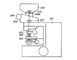
図1は、本発明の第1の実施の形態に係る光学装置用デジタルカメラの搭載された顕微鏡を示す図である。顕微鏡本体201には、標本206の位置決めが可能なステージ202が光軸方向に昇降自在に設けられている。更に、顕微鏡本体201には、ステージ202に対向して標本像を拡大するための対物レンズ203と、結像レンズ207及び目視観察のための接眼レンズ204を装着した鏡筒205とが組合せ配置される。そして、結像レンズ207の後段には、光学装置用デジタルカメラを構成するカメラ本体208が配設される。
【0018】
上記構成により、標本像を取得する場合には、ステージ202上に標本206を載置して、ステージ202を上下動させ、対物レンズ203の焦点位置に標本を合わせると、結像レンズ、接眼レンズにより標本の拡大像が観察可能となる。同時に、結像レンズによりカメラ本体208のCCD素子(固体撮像素子)209の撮像面209aに標本の拡大像が結像されて、標本画像が取得される。
【0019】
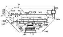
カメラ本体208は、図2に示すように下側外装106と上側外装117を備えている。密閉容器を構成する下側外装106には、取付用のメスネジ部108が、鏡筒205に設けられた図示しないオスネジ に対応して設けられている。メスネジ部108が鏡筒205のオスネジに螺合されて顕微鏡本体201に組付けられる。
【0020】
CCD素子209は、カメラ本体208内に収容配置されたCCD素子用プリント基板101に半田接続されて搭載される。そして、CCD素子209の背面209bには、電圧印加で熱の移動を行うペルチェ素子102が熱伝導率の高い熱伝導性弾性部材103を介して熱的に結合される。このペルチェ素子102は、後述する変位部材105に取付け配置される。なお、熱伝導性の高い弾性部材103の材質等は特に限定されないが、例えば、信越シリコーン(株)製 高熱伝導性ゴムシートのような熱伝導性の優れた弾性部材であればどのような材料を用いても良い。
【0021】
変位部材105とCCD素子用プリント基板101との間には、スペーサ104が介在される。ペルチェ素子102と高熱伝導性弾性部材103の長さよりも、CCD素子209の背面209bからCCD素子用プリント基板101の取付面101aとスペーサ104の長さを足した長さが短くなるように、スペーサ104の長さが設定される。これにより、上記変位部材105とプリント基板101とを、ビス120aを用いて固定すると、ペルチェ素子102は、高熱伝導性弾性部材103が変形して密着した状態で、プリント基板101が変位部材105に固定される。そのため、各部材間の熱抵抗は、低い状態で固定される。変位部材105は、下側外装106にビスを用いて固定される。
【0022】
また、下側外装106には、映像を取り込むためのガラス部材115が、固定部材107を介して下側外装106のメスネジ部108内に固定配置される。そして、ガラス部材115と下側外装106の密閉を高めるために、下側外装106には、溝106aがガラス部材115の一方の面に対向して形成されている。溝106aには、弾性を有するゴム材料よりなるOリング110が挿着される。
【0023】
Oリング110の線径は、上記溝106aの深さより約30%太く設定され、溝106aに収容されると、ガラス部材115の一方の面でつぶされた状態で固定される。これにより、小さな隙間も埋めることができるので、高い密閉性を得ることが可能となる。
【0024】
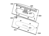
また、下側外装106には、メスネジ部108と逆側に溝106bが設けられている。溝106bには、Oリング112が挿着される。そして、溝106bのうえから中蓋109が被着される。溝106bとOリング112の大きさは、それぞれ上述した溝106a及びOリング110と同様の大きさに設定されて、上記と同様に所望の密閉性を有するように設置される。この中蓋109を介してケーブル111が基板114に接続される様子を図3に示す。図3は、図2のA部を拡大して示す分解斜視図である。
【0025】
中蓋109には、図3に示すようにケーブル挿通用の四角形状の長孔109aが設けられている。長孔109aの周囲には、6本の基板固定用スタッド113と、Oリング302位置決め用の2本の位置決め用スタッド301がそれぞれ溶接等により所定の間隔に固着される。位置決め用スタッド301間には、Oリング302が引伸ばされた状態で取り付けられる。
【0026】
スタッド113、301の高さとOリング302の線径は、
Oリング302の線径>スタッド113高さ>スタッド301高さ
に設定される。これにより、制御用プリント基板114を中蓋109にビス120bを用いてビス固定すると、スタッド113の高さまでOリング302は、全周均等に潰される。
【0027】
制御用プリント基板114は、外部コネクタ118を介して外部の図示しないパソコンと外部接続される。制御用プリント基板114の内面側に図4に示すように表面実装タイプのコネクタ304が搭載される。そして、コネクタ304は、ケーブル111を介してCCD素子用プリント基板101と電気的に接続される。
【0028】
制御用プリント基板114には、ビス孔303がスタッド113に対応してOリング302の接触範囲内(図3及び図4において、破線Aで囲まれた部分。以下、「破線A」とのみ称する)を除いた部位に形成され(図4参照)、このビス孔303を通してビス120bがスタッド113に螺着されて固定される。
【0029】
即ち、制御用プリント基板114には、ビス孔303の他、多層基板で各層を導通させるためのスルーホール400が上記接触範囲(破線A)内の外側に形成される。また、制御用プリント基板114に使用されるコネクタ304は、上述したように表面実装タイプであることから、上記接触範囲(破線A)内に孔は無く通気性はほとんどない。そして、制御用プリント基板114は、基板製造上、その表面に樹脂材料のレジスト膜が塗布されている。このため、仮に通気性のあるガラスエポキシ材料で形成した場合においても、密閉容器として使用する範囲である上記接触範囲(破線A)内にレジスト膜を通過する孔が存在しない。従って、プリント基板114が密閉容器の一部として機能し、所望の密閉構造が実現される。
【0030】
上記構成により、CCD素子209、ペルチェ素子102、高熱伝導性弾性部材103は、密閉容器を構成する下側外装106、ガラス部材115、中蓋109、制御用プリント基板114と各Oリング110、112、302により密閉されて外気から遮断される。
【0031】
また、密閉容器を構成する中蓋109の内面に所定量のシリカゲル等の乾燥剤116が取り付けられる。これにより、密閉容器内は、作業時に取り込んだ湿気や、わずかな隙間より侵入する湿気が乾燥剤116により除湿されて密閉容器内部が低湿度に保たれる。これにより、密閉容器内の湿気による露点より低い温度まで冷却しない限り、外部の湿度に影響なく、CCD素子209の撮像面209aに結露が発生することがない。
【0032】
また、密閉容器の一部をスルーホール等の孔の無い制御用プリント基板114で構成している。これにより、密閉容器内外の電気的接続のために従来のようなフラットケーブルなどの特殊な部品を設ける必要がない。従って、電流容量も多く取ることができ、多様な構成を採ることが可能となる。
【0033】
ここで、変位部材105について説明する。変位部材105は、図5に示すように変位部位105a、固定部位105b、両者を連結するヒンジ部105cで構成され、例えばワイヤーカット加工法により一体的に形成される。そして、変位部位105aと固定部位105bとの間の直角な2方向には、変位手段を構成するピエゾ素子500が接着されている。
【0034】
ピエゾ素子500は、印加電圧に比例して変位する性質を有する。そして、印加電圧を図示しない制御部を介して制御することで、変位部材105の変位部位105aを任意量変位させることができる。これにより、変位部位105aに支持されるCCD素子209がピエゾ素子500の変位に連動して2次元に移動制御される。
【0035】
また、変位部材105には、CCD素子209と高熱伝導性弾性部材103が熱的に結合されて取り付けられている。これにより、変位部材105は、CCD素子209を冷却するためペルチェ素子102が移動した熱を伝達する。すると、変位部材105によって伝達された熱は、下側外装106に伝達されて、最終的に外気に放熱される。このように、ペルチェ素子102の放熱経路は、変位部材105、下側外装106で構成されている。これにより、少ない部品で、且つ、放熱経路が機械的結合のみで構成されることにより、熱抵抗を低く抑えた放熱経路を実現できる。
【0036】
このように、本実施形態に係る光学装置用デジタルカメラは、撮影するためのCCD素子209と、CCD素子209を冷却するCCD素子冷却手段を構成するペルチェ素子102とを密閉する密閉容器の一部を制御用プリント基板114で形成するように構成した。
【0037】
これによれば、密閉容器の一部を構成する制御用プリント基板114を介して、外部接続が可能となる。これにより、従来のように外部接続部品として専用ケーブルを用いた密閉構造のものを用いる必要がなくなる。このため、暗電流の低減と、結露防止とを実現したうえで、電流容量による制約を受けない基板構成が可能となる。
【0038】
また、本実施形態に係る光学装置用デジタルカメラは、CCD素子209と、CCD素子209を変位可能に支持する変位部材105とを、ペルチェ素子102を介して構成している。
【0039】
これにより、CCD素子209を冷却させるためにペルチェ素子102で移動した熱は、変位部材105を介して密閉容器を構成する下側外装106に伝達され放熱される。これにより、ペルチェ素子102の放熱経路を新たに設ける必要がないため、変位部材の負荷を軽減でき、かつ部品の削減が可能となる。
【0040】
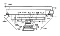
上記の第1の実施の形態では、密閉容器の一部を中蓋109及び制御用プリント基板114で構成した場合で説明したが、これに限ることなく、図6に示すように制御用プリント基板600で直接的に下側外装を閉塞して密閉容器を構成するように構成することも可能である。図6は、本発明の第2の実施の形態に係る光学装置用デジタルカメラの要部を示した構成図である。但し、図6においては、便宜上、図1乃至図5と同一部分について、同一符号を付して、その詳細な説明を省略する。
【0041】
即ち、上記下側外装106の溝106bには、Oリング112が挿着され、その上から制御用プリント基板600をビス固定する。これにより、制御用プリント基板600上の凹凸や、下側外装106の小さな隙間は、第1の実施形態と同様に封止されて密閉構造が形成される。
【0042】
第2の実施形態によれば、第1の実施の形態における中蓋109、Oリング112を省略することが可能となる。なお、第2の実施の形態においては、制御用プリント基板600の各層間の接続は全ての基板間を貫通する孔を設けるのでなく、例えば4枚の基板構成では3枚のみを貫通する孔を設け、前記孔には埋め込みビアと呼ばれる導通性のある部材を挿入し、3枚の導通を取る手段を用いることになる。
【0043】
また、上記の各実施の形態においては、光学装置のうち顕微鏡に適用した場合で説明したが、本発明は、これに限ることなく、その他の光学装置に適用することも可能である。また、上記の実施形態では、ペルチェ素子102を変位部材105に取り付けるものとしたが、高解像度の必要がなければ、単にペルチェ素子102からの熱を下側外装106に伝達するための熱伝導性部材、例えばアルミや真鍮といった金属板であっても良い。
【0044】
本発明は、上記各実施の形態に限ることなく、その他、実施段階ではその要旨を逸脱しない範囲で種々の変形を実施し得ることが可能である。さらに、上記各実施形態には、種々の段階の発明が含まれており、開示される複数の構成要件における適宜な組合せにより種々の発明が抽出され得る。
【0045】
本発明の一局面に係る光学装置用デジタルカメラは、対象物を撮像するための固体撮像素子と、前記固体撮像素子を冷却する固体撮像素子冷却手段と、電気信号配線用のプリント基板を含み、前記固体撮像素子と前記固体撮像素子冷却手段とを密閉する密閉手段と、を具備することを特徴とする。なお、前記固体撮像素子冷却手段は、ペルチェ素子と、熱伝導性部材と、を有することが好ましい。
【0046】
本発明の一局面に係る光学装置用デジタルカメラの好ましい実施態様は以下の通りである。なお、以下の各実施態様は、それぞれ独立して適用しても良いし、適宜組み合わせて適用しても良い。
【0047】
(1) 前記ペルチェ素子と前記固体撮像素子との間に配置された熱良導体の弾性部材を更に備えたこと。
【0048】
(2)前記プリント基板は、電気接続のためのコネクタと、スルーホールと、取付孔と、を有し、前記コネクタは、前記密閉手段の蓋部として機能する部分に取り付けられ、前記スルーホール及び取付孔は、前記密閉手段の蓋部として機能する部分以外の場所に取り付けられること。
【0049】
(3) (2)において、前記外装は、前記プリント基板のコネクタに接続されるコネクタ用配線が貫通する開口部を有する中蓋を備え、前記プリント基板は、前記中蓋の開口部を密封すること。
【0050】
(4) 前記密閉手段は、前記固体撮像素子冷却手段を覆う外装を更に備え、前記プリント基板は、前記外装の開口部を封止する蓋として機能すること。
【0051】
(5) (4)において、前記固体撮像素子で発生した熱は、前記弾性部材、前記ペルチェ素子、熱伝導性部材及び前記外装を介して外部に放出されること。
【0052】
(6) (5)において、前記熱伝導性部材は変位部材であること。
【0053】
(7) (4)において、前記プリント基板は、電気接続のためのコネクタと、スルーホールと、取付孔と、を有し、前記コネクタは、前記外装の開口部に取り付けられ、前記スルーホール及び取付孔は、前記外装の開口部以外の場所に取り付けられること。
【0054】
上記の実施形態によれば、密閉容器の一部を構成するプリント基板より、外部接続が可能となることにより、外部接続用接続部品として専用ケーブルを用いた密閉構造のものを用いることがなくなる。従って、暗電流の防止と共に、結露防止を実現したうえで、電流容量による制約を受けない基板構成が可能となる。
【0055】
上記の実施形態によれば、固体撮像素子冷却手段により固体撮像素子で生じた熱は、変位手段を介して外部に放熱させるため、解像度の向上を図った上で、固体撮像素子の暗電流の軽減が可能となる。
【0056】
上記の実施形態によれば、プリント基板で一部を直接的に閉塞した密閉手段を構成することが可能となる。これにより、部品点数の軽減が図れ、組立て作業の簡略化の促進が図れる。
【0057】
また、例えば各実施形態に示される全構成要件から幾つかの構成要件が削除されても、発明が解決しようとする課題の欄で述べた課題が解決でき、発明の効果で述べられている効果が得られる場合には、この構成要件が削除された構成が発明として抽出され得る。
【0058】
例えば、上記実施の形態に基づいて光学装置に用いられるデジタルカメラであって、CCD素子を微動量変位させるための弾性ヒンジを有した一体式の変位部材と、前記変位部材を微小量変位させる駆動手段と、前記CCD素子を冷却するための冷却手段と、前記冷却手段により冷却される冷却部を外気より遮断する密閉容器と、を具備し、前記密閉容器の一部がガラスエポキシよりなるプリント基板にて構成されることを特徴とする光学装置用デジタルカメラを提供することができる。
【0059】
なお、上述した実施形態では、下側外装106に密閉を目的としてガラス部材115が固定されていたが、更に密閉以外の目的としてガラス部材115にフィルタ機能、例えばIRカットフィルタの機能を付加させることも可能である。
【0060】
このようにすることにより、例えば、第1の実施形態にIRカットフィルタの機能が求められていた場合、下側外装106に固定配置されるガラス部材115には、フィルタの機能がないので、フィルタを別体の光学部材として光路中に固定配置することとなるが、ガラス部材自体にフィルタ機能を一体的に付加するようにしたことで、別体の光学部材を設ける必要がなくなり、構成の簡素化及びコストの低減化を実現できる。
【0061】
【発明の効果】
以上詳述したように、本発明によれば、撮像素子の冷却が効率的かつ確実に行えると共に、構成簡易にして、電流容量による制約を受けない構成が可能であり、且つ、暗電流の発生を低減して、高画質化の促進を図り得るようにした光学装置用デジタルカメラを提供することができる。
【図面の簡単な説明】
【図1】 本発明の第1の実施の形態に係る光学装置用デジタルカメラを顕微鏡に組付けた状態を示した配置図。
【図2】 本発明の第1の実施の形態に係る光学装置用デジタルカメラを示した構成図。
【図3】 図2の要部を拡大して示した詳細説明図。
【図4】 図2の制御用プリント基板を取り出し示した詳細説明図。
【図5】 図2の変位部材を取り出した詳細説明図。
【図6】 本発明の第2の実施の形態に係る光学装置用デジタルカメラの要部を示した構成図。
【符号の説明】
101a…取付面
101…プリント基板
102…ペルチェ素子
103…弾性部材
104…スペーサ
105…変位部材
105a…変位部位
105b…固定部位
105c…ヒンジ部
106…下側外装
106a、106b…溝
107…固定部材
108…メスネジ部
109…中蓋
109a…長孔
110…Oリング
111…ケーブル
112…Oリング
113…スタッド
114…プリント基板
115…ガラス部材
116…乾燥剤
117…上側外装
118…外部コネクタ
120a…ビス
120b…ビス
201…顕微鏡本体
202…ステージ
203…対物レンズ
204…接眼レンズ
205…鏡筒
206…標本
207…結像レンズ
208…カメラ本体
209…CCD素子
209a…撮像面
209b…背面
301…スタッド
302…Oリング
303…ビス孔
304…コネクタ
400…スルーホール
500…ピエゾ素子
600…プリント基板[0001]
BACKGROUND OF THE INVENTION
The present invention relates to a digital camera for an optical apparatus suitable for an optical apparatus such as a microscope.
[0002]
[Prior art]
In microscopic observation, high-quality images are required for performing pathological diagnosis in which diagnosis is performed according to cell morphology, fluorescence imaging in which changes in specimens are measured by weak fluorescence, and the like. As a means for obtaining an image, there is a digital camera system using a solid-state image pickup device such as a CCD device (hereinafter referred to as “CCD device”) instead of a conventional camera system using a silver salt film as an image pickup medium. It has come to be used.
[0003]
A CCD element as an imaging medium has a dark current in which a minute output current flows even when there is no light input. The dark current increases depending on the temperature rise and becomes noise to the image signal, and as a result, SN is lowered. For this reason, a method is adopted in which the dark current is reduced by cooling the CCD element to improve the SN of the image signal.
[0004]
However, when the outside of the CCD element is touched with high humidity in the cooled state, the surface of the CCD element is condensed and moisture is attached. As a result, the image deteriorates or the peripheral device malfunctions. For this purpose, a sealed structure is adopted in which the CCD element is arranged in a sealed container with low humidity.
[0005]
The following technique is known as a conventional sealed structure (see Japanese Patent Laid-Open No. 6-45570).
[0006]
That is, this sealed structure is configured as follows. There is no air permeability, and the cable is drawn out from between the sealed containers divided into two using a cable made of a thin film material. And by inserting an O-ring between the cables, the gap is filled and sealed.
[0007]
However, since the above-described sealed structure has to produce a dedicated cable, it is expensive and it is difficult to increase its current capacity.
[0008]
By the way, since the CCD element includes light receiving elements arranged in a two-dimensional manner, the resolution is determined by the total number of light receiving elements. However, if the number of CCD elements is increased by increasing the number of the CCD elements in order to increase the resolution of the light receiving elements, the sensitivity is lowered and the cost is increased.
[0009]
As a means to improve the image quality of the image signal acquired by the CCD element, the CCD element with a small number of pixels is moved two-dimensionally to improve the number of pixels without lowering the sensitivity, thereby improving the image quality. A technique to be realized is disclosed (see Japanese Patent Laid-Open No. 9-21867).
[0010]
In the above technique, a plate-like metal member is bent and a CCD element is assembled to a displacement mechanism using the elastic force. Then, by moving the CCD element two-dimensionally via the displacement mechanism, the number of pixels is improved without reducing the sensitivity.
[0011]
However, no means for reducing the dark current of the CCD element has been proposed as means for improving the image quality of the CCD element.
[0012]
As described above, the conventional sealed structure of the CCD element requires the production of a dedicated connection cable and has a limitation of the substrate configuration due to the current capacity. In addition, the means for improving the image quality of the conventional CCD element is not possible. Although the resolution can be improved, the dark current increases and the SN is lowered.
[0013]
[Problems to be solved by the invention]
SUMMARY OF THE INVENTION An object of the present invention is to provide a digital camera for an optical device that has a simple configuration, can improve the current capacity, and can prevent the occurrence of dark current and promote the enhancement of image quality. And
[0014]
[Means for solving the problems]
A digital camera for an optical apparatus according to the present invention includes a solid-state image sensor for imaging an object, a solid-state image sensor cooling means for cooling the solid-state image sensor , a printed circuit board for electric signal wiring, and the electric signal wiring. The printed circuit board for use constitutes a part of the sealing means for sealing the solid-state image sensor and the solid-state image sensor cooling means.
[0015]
DETAILED DESCRIPTION OF THE INVENTION
Embodiments of the present invention will be described with reference to the drawings.
[0016]
Hereinafter, embodiments of the present invention will be described in detail with reference to the drawings.
[0017]
FIG. 1 is a diagram showing a microscope equipped with a digital camera for an optical device according to a first embodiment of the present invention. The microscope
[0018]
With the above configuration, when acquiring a specimen image, the specimen 206 is placed on the stage 202, the stage 202 is moved up and down, and the specimen is aligned with the focal position of the
[0019]
The
[0020]
The
[0021]
A
[0022]
In addition, a
[0023]
The wire diameter of the O-
[0024]
Further, the
[0025]
As shown in FIG. 3, the
[0026]
The height of the
The wire diameter of the O-
[0027]
The control printed
[0028]
In the printed
[0029]
That is, in the control printed
[0030]
With the above configuration, the
[0031]
A predetermined amount of a desiccant 116 such as silica gel is attached to the inner surface of the
[0032]
Further, a part of the hermetic container is constituted by a control printed
[0033]
Here, the
[0034]
The
[0035]
Further, a
[0036]
As described above, the digital camera for an optical apparatus according to the present embodiment is a part of a sealed container that seals the
[0037]
According to this, external connection becomes possible via the printed
[0038]
In the digital camera for an optical apparatus according to the present embodiment, a
[0039]
Thereby, the heat moved by the
[0040]
In the first embodiment, the case where a part of the hermetic container is configured by the
[0041]
That is, an O-
[0042]
According to the second embodiment, the
[0043]
In each of the above-described embodiments, the description has been given of the case where the optical device is applied to a microscope. However, the present invention is not limited to this and can be applied to other optical devices. In the above embodiment, the
[0044]
The present invention is not limited to the above-described embodiments, and various modifications can be made without departing from the scope of the invention at the stage of implementation. Further, the above embodiments include inventions at various stages, and various inventions can be extracted by appropriately combining a plurality of disclosed constituent elements.
[0045]
A digital camera for an optical device according to an aspect of the present invention includes a solid-state image sensor for imaging an object, a solid-state image sensor cooling means for cooling the solid-state image sensor, and a printed circuit board for electric signal wiring. A sealing means for sealing the solid-state image sensor and the solid-state image sensor cooling means is provided. In addition, it is preferable that the said solid-state image sensor cooling means has a Peltier device and a heat conductive member.
[0046]
Preferred embodiments of the digital camera for an optical device according to one aspect of the present invention are as follows. The following embodiments may be applied independently or may be applied in appropriate combination.
[0047]
(1) An elastic member having a good thermal conductor disposed between the Peltier element and the solid-state imaging element is further provided.
[0048]
(2) The printed circuit board includes a connector for electrical connection, a through hole, and an attachment hole, and the connector is attached to a portion that functions as a lid portion of the sealing means, The attachment hole should be attached to a place other than the portion functioning as the lid of the sealing means.
[0049]
(3) In (2), the exterior includes an inner lid having an opening through which a connector wiring connected to the connector of the printed board passes, and the printed board seals the opening of the inner lid. thing.
[0050]
(4) The sealing means further includes an exterior covering the solid-state image sensor cooling means, and the printed circuit board functions as a lid for sealing the opening of the exterior.
[0051]
(5) In (4), the heat generated in the solid-state imaging device is released to the outside through the elastic member, the Peltier device, the heat conductive member, and the exterior.
[0052]
(6) In (5), the thermally conductive member is a displacement member.
[0053]
(7) In (4), the printed circuit board has a connector for electrical connection, a through hole, and an attachment hole, and the connector is attached to the opening of the exterior, and the through hole and The attachment hole should be attached to a place other than the opening of the exterior.
[0054]
According to the embodiment described above, external connection is possible from the printed circuit board constituting a part of the sealed container, so that a sealed structure using a dedicated cable is not used as a connection component for external connection. Therefore, it is possible to realize a substrate configuration that is not restricted by current capacity while preventing dark current and preventing condensation.
[0055]
According to the above embodiment, the heat generated in the solid-state image sensor by the solid-state image sensor cooling means is dissipated to the outside through the displacement means. Therefore, after improving the resolution, the dark current of the solid-state image sensor is reduced. Mitigation is possible.
[0056]
According to the above embodiment, it is possible to configure a sealing means in which a part is directly closed with a printed circuit board. As a result, the number of parts can be reduced, and the assembly work can be simplified.
[0057]
In addition, for example, even if some structural requirements are deleted from all the structural requirements shown in each embodiment, the problem described in the column of the problem to be solved by the invention can be solved, and the effect described in the effect of the invention Can be obtained as an invention.
[0058]
For example, a digital camera used in an optical device based on the above embodiment, an integrated displacement member having an elastic hinge for finely displacing a CCD element, and a drive for displacing the displacement member by a small amount A printed circuit board comprising: a means; a cooling means for cooling the CCD element; and a sealed container that blocks a cooling part cooled by the cooling means from outside air, wherein a part of the sealed container is made of glass epoxy. It is possible to provide a digital camera for an optical device characterized by comprising
[0059]
In the above-described embodiment, the
[0060]
By doing so, for example, when the function of the IR cut filter is required in the first embodiment, the
[0061]
【The invention's effect】
As described above in detail, according to the present invention, the image sensor can be cooled efficiently and reliably, the configuration can be simplified, and a configuration that is not restricted by the current capacity is possible, and the generation of dark current is possible. Thus, it is possible to provide a digital camera for an optical apparatus that can promote the enhancement of the image quality.
[Brief description of the drawings]
FIG. 1 is a layout view showing a state in which a digital camera for an optical device according to a first embodiment of the present invention is assembled to a microscope.
FIG. 2 is a configuration diagram showing a digital camera for an optical device according to the first embodiment of the present invention.
FIG. 3 is a detailed explanatory view showing an enlarged main part of FIG. 2;
4 is a detailed explanatory view showing the control printed circuit board shown in FIG. 2 taken out. FIG.
FIG. 5 is a detailed explanatory view showing the displacement member in FIG. 2 taken out.
FIG. 6 is a configuration diagram showing a main part of a digital camera for an optical device according to a second embodiment of the present invention.
[Explanation of symbols]
DESCRIPTION OF
Claims (9)
前記固体撮像素子を冷却する固体撮像素子冷却手段と、
電気信号配線用のプリント基板と、
前記電気信号配線用のプリント基板が前記固体撮像素子及び固体撮像素子冷却手段を密閉する密閉手段の一部を構成していることを特徴とする光学装置用デジタルカメラ。A solid-state image sensor for imaging an object;
A solid-state image sensor cooling means for cooling the solid-state image sensor;
A printed circuit board for electrical signal wiring;
The digital camera for an optical apparatus, wherein the printed circuit board for electrical signal wiring constitutes a part of a sealing means for sealing the solid-state image sensor and the solid-state image sensor cooling means .
前記プリント基板は、電気接続のためのコネクタと、スルーホールと、取付孔と、を有し、
前記コネクタは、前記密閉手段の蓋部として機能する部分に取り付けられ、
前記スルーホール及び取付孔は、前記密閉手段の蓋部として機能する部分以外の場所に取り付けられることを特徴とする光学装置用デジタルカメラ。In the digital camera for optical devices according to claim 1 or 2,
The printed circuit board has a connector for electrical connection, a through hole, and a mounting hole,
The connector is attached to a portion that functions as a lid of the sealing means,
The digital camera for an optical device, wherein the through hole and the attachment hole are attached to a place other than a portion functioning as a lid portion of the sealing means.
前記プリント基板のコネクタに接続されるコネクタ用配線が貫通する開口部を有する中蓋を備え、
前記プリント基板は、前記中蓋の開口部を密封することを特徴とする光学装置用デジタルカメラ。In the digital camera for optical devices according to claim 4,
Comprises a inner lid of the wiring connector is connected to a printed circuit board connector having an opening therethrough,
The digital camera for an optical device, wherein the printed circuit board seals an opening of the inner lid.
前記密閉手段は、前記固体撮像素子冷却手段を覆う外装を更に備え、
前記プリント基板は、前記外装の開口部を封止する蓋として機能することを特徴とする光学装置用デジタルカメラ。The digital camera for an optical device according to any one of claims 1, 2 and 3,
The sealing means further includes an exterior covering the solid-state image sensor cooling means,
The digital camera for an optical apparatus, wherein the printed circuit board functions as a lid for sealing the opening of the exterior.
前記プリント基板は、電気接続のためのコネクタと、スルーホールと、取付孔と、を有し、
前記コネクタは、前記外装の開口部に取り付けられ、
前記スルーホール及び取付孔は、前記外装の開口部以外の場所に取り付けられることを特徴とする光学装置用デジタルカメラ。The digital camera for an optical device according to claim 6,
The printed circuit board has a connector for electrical connection, a through hole, and a mounting hole,
The connector is attached to the opening of the exterior,
The digital camera for an optical device, wherein the through hole and the attachment hole are attached to a place other than the opening of the exterior.
Priority Applications (1)
| Application Number | Priority Date | Filing Date | Title |
|---|---|---|---|
| JP2002348837A JP3944446B2 (en) | 2001-11-29 | 2002-11-29 | Digital camera for optical equipment |
Applications Claiming Priority (3)
| Application Number | Priority Date | Filing Date | Title |
|---|---|---|---|
| JP2001-365018 | 2001-11-29 | ||
| JP2001365018 | 2001-11-29 | ||
| JP2002348837A JP3944446B2 (en) | 2001-11-29 | 2002-11-29 | Digital camera for optical equipment |
Publications (3)
| Publication Number | Publication Date |
|---|---|
| JP2003230031A JP2003230031A (en) | 2003-08-15 |
| JP2003230031A5 JP2003230031A5 (en) | 2005-08-11 |
| JP3944446B2 true JP3944446B2 (en) | 2007-07-11 |
Family
ID=27759485
Family Applications (1)
| Application Number | Title | Priority Date | Filing Date |
|---|---|---|---|
| JP2002348837A Expired - Lifetime JP3944446B2 (en) | 2001-11-29 | 2002-11-29 | Digital camera for optical equipment |
Country Status (1)
| Country | Link |
|---|---|
| JP (1) | JP3944446B2 (en) |
Families Citing this family (3)
| Publication number | Priority date | Publication date | Assignee | Title |
|---|---|---|---|---|
| JP4722505B2 (en) * | 2005-02-10 | 2011-07-13 | オリンパス株式会社 | Imaging device |
| JP4626474B2 (en) * | 2005-10-12 | 2011-02-09 | 株式会社ニコン | Electronic camera and microscope with cooling control function |
| JP5896650B2 (en) * | 2011-08-31 | 2016-03-30 | オリンパス株式会社 | Imaging device |
-
2002
- 2002-11-29 JP JP2002348837A patent/JP3944446B2/en not_active Expired - Lifetime
Also Published As
| Publication number | Publication date |
|---|---|
| JP2003230031A (en) | 2003-08-15 |
Similar Documents
| Publication | Publication Date | Title |
|---|---|---|
| US11887839B2 (en) | Imaging unit and imaging apparatus | |
| WO2021164519A1 (en) | Camera module and electronic device | |
| JP4083521B2 (en) | Imaging device | |
| JP4438737B2 (en) | Portable electronic devices | |
| US8106952B2 (en) | Imaging device unit and imaging apparatus | |
| RU2575944C2 (en) | Electronic component and electronic device | |
| JP2004120583A (en) | Image pickup apparatus | |
| JP5871534B2 (en) | Imaging device | |
| KR20110064156A (en) | Imaging device and its manufacturing method | |
| JP5117967B2 (en) | Electronic equipment and electronic equipment with imaging function | |
| CN101916766B (en) | Imaging device module and portable electronic apparatus utilizing the same | |
| JP2008219704A (en) | Semiconductor device | |
| JP4722505B2 (en) | Imaging device | |
| JP6218469B2 (en) | Imaging device | |
| JP3944446B2 (en) | Digital camera for optical equipment | |
| CN110290293B (en) | Photosensitive module | |
| KR102413918B1 (en) | Camera module, manufacturing method and electronic device | |
| WO2020220815A1 (en) | Camera module and photosensitive assembly thereof, and electronic device and preparation method | |
| CN216817067U (en) | Optical element driving mechanism | |
| US7545437B2 (en) | Digital camera for an optical apparatus including a cooling mechanism for a solid-state imaging device | |
| JP5896650B2 (en) | Imaging device | |
| JP2014225580A (en) | Imaging unit and imaging apparatus | |
| US20230413426A1 (en) | Circuit board assembly for blocking unwanted light, camera module, and electronic device having the same | |
| JP5896697B2 (en) | Microscope imaging device | |
| JP2018125582A (en) | Fine adjustment device |
Legal Events
| Date | Code | Title | Description |
|---|---|---|---|
| A521 | Request for written amendment filed |
Free format text: JAPANESE INTERMEDIATE CODE: A523 Effective date: 20050126 |
|
| A621 | Written request for application examination |
Free format text: JAPANESE INTERMEDIATE CODE: A621 Effective date: 20050126 |
|
| A977 | Report on retrieval |
Free format text: JAPANESE INTERMEDIATE CODE: A971007 Effective date: 20061222 |
|
| A131 | Notification of reasons for refusal |
Free format text: JAPANESE INTERMEDIATE CODE: A131 Effective date: 20070116 |
|
| A521 | Request for written amendment filed |
Free format text: JAPANESE INTERMEDIATE CODE: A523 Effective date: 20070307 |
|
| TRDD | Decision of grant or rejection written | ||
| A01 | Written decision to grant a patent or to grant a registration (utility model) |
Free format text: JAPANESE INTERMEDIATE CODE: A01 Effective date: 20070403 |
|
| A61 | First payment of annual fees (during grant procedure) |
Free format text: JAPANESE INTERMEDIATE CODE: A61 Effective date: 20070409 |
|
| R151 | Written notification of patent or utility model registration |
Ref document number: 3944446 Country of ref document: JP Free format text: JAPANESE INTERMEDIATE CODE: R151 |
|
| FPAY | Renewal fee payment (event date is renewal date of database) |
Free format text: PAYMENT UNTIL: 20110413 Year of fee payment: 4 |
|
| FPAY | Renewal fee payment (event date is renewal date of database) |
Free format text: PAYMENT UNTIL: 20120413 Year of fee payment: 5 |
|
| FPAY | Renewal fee payment (event date is renewal date of database) |
Free format text: PAYMENT UNTIL: 20130413 Year of fee payment: 6 |
|
| FPAY | Renewal fee payment (event date is renewal date of database) |
Free format text: PAYMENT UNTIL: 20140413 Year of fee payment: 7 |
|
| S531 | Written request for registration of change of domicile |
Free format text: JAPANESE INTERMEDIATE CODE: R313531 |
|
| R350 | Written notification of registration of transfer |
Free format text: JAPANESE INTERMEDIATE CODE: R350 |
|
| R250 | Receipt of annual fees |
Free format text: JAPANESE INTERMEDIATE CODE: R250 |
|
| R250 | Receipt of annual fees |
Free format text: JAPANESE INTERMEDIATE CODE: R250 |