JP3934191B2 - Semiconductor manufacturing equipment - Google Patents
Semiconductor manufacturing equipment Download PDFInfo
- Publication number
- JP3934191B2 JP3934191B2 JP35408796A JP35408796A JP3934191B2 JP 3934191 B2 JP3934191 B2 JP 3934191B2 JP 35408796 A JP35408796 A JP 35408796A JP 35408796 A JP35408796 A JP 35408796A JP 3934191 B2 JP3934191 B2 JP 3934191B2
- Authority
- JP
- Japan
- Prior art keywords
- substrate
- speed
- chamber
- transfer
- acceleration
- Prior art date
- Legal status (The legal status is an assumption and is not a legal conclusion. Google has not performed a legal analysis and makes no representation as to the accuracy of the status listed.)
- Expired - Lifetime
Links
Images


Description
【0001】
【発明の属する技術分野】
本発明は、複数のチャンバを備えた半導体製造装置において、複数のチャンバに対する基板の搬送処理を行う基板搬送装置に関する。
【0002】
【従来の技術】
半導体製造装置には、半導体ウェーハやガラス基板等といった処理対象の基板に対して複数の所定の処理を施すために、複数のチャンバを備え、各チャンバ間の基板の搬送処理を基板搬送装置によって行わせるものがある。
このような半導体製造装置を図3に示す当該装置の一部分を参照して説明する。
この半導体製造装置は、基板に対して所定の処理を施すプロセスチャンバPC1〜PC3と、チャンバ間の基板の搬送処理を行う基板搬送装置Jと、を備えている。
【0003】
プロセスチャンバPC1〜PC3は、互いに異なる処理を行うチャンバとなっており、チャンバの形状が異なっている。
基板搬送装置Jは、基板を載置保持する基板保持手段Tと、回転及び伸縮動作を行うことによって基板保持手段Tを移動させる駆動手段Rと、を備え、各チャンバに対する基板の搬入処理及び搬出処理を予め設定された同一の搬送速度及び搬送加速度に基づいて行っている。
【0004】
例えば、プロセスチャンバPC1へ基板を搬入する場合には、前記設定に基づいた回転及び伸長動作によって駆動手段Rが基板を載置保持した基板保持手段TをプロセスチャンバPC1内に移動させ、所定の基板載置位置に基板保持手段Tが保持する基板を載置させる。次いで、前記設定に基づいた収縮動作によって駆動手段Rが基板保持手段TをプロセスチャンバPC1外に移動させる。
【0005】
一方、プロセスチャンバPC1から基板を搬出する場合には、前記設定に基づいた回転及び伸長動作によって駆動手段RがプロセスチャンバPC1内に移動させ、所定の基板載置位置の基板を基板保持手段Tに載置させる。次いで、前記設定に基づいた収縮動作によって駆動手段Rが基板を載置保持した基板保持手段TをプロセスチャンバPC1外に移動させる。
そして、他のチャンバに対しても予め設定された前記同一の搬送速度及び搬送加速度に基づいて基板の搬送処理を行っている。
なお、駆動装置Rが複数の機構(軸)で構成されている場合には、上記した搬送速度及び搬送加速度として、各軸毎の速度及び加速度が設定されている場合がある。
【0006】
なお、特開平7−307373号公報に記載された発明では、ウエハ(基板)の搬送処理において、ウエハが保持されているか否かによって、速度及び加速度を変えることによって、搬送処理の処理効率を向上させることが記載されている。
【0007】
【発明が解決しようとする課題】
半導体製造装置では、基板の搬送処理に要する時間を短縮して処理効率を向上させることが望まれており、このために、上記した基板搬送装置では、搬送速度を速く、搬送加速度を大きくすることが行われている。
【0008】
しかしながら、上記した従来の基板搬送装置においては、駆動装置が伸長する長さが長くなるほど、基板保持手段に与える振動が大きくなり、搬送速度が速く又は搬送加速度が大きくなるほど振動が基板保持手段の基板に与える影響が大きくなるといった傾向にあり、基板保持手段が基板を保持している際の搬送速度及び搬送加速度は、駆動装置による最も長い伸長動作を必要とするチャンバに対する搬送処理において、基板のずれ、基板の脱落等といった事態を防止できるものでなければならず、時間の短縮にも限度があった。
【0009】
そこで、本発明は、従来の事情に鑑みなされたもので、搬送処理において基板のずれを防止するとともに基板搬送処理の処理効率をさらに向上することのできる基板搬送装置を提供することを目的としている。
【0010】
【課題を解決するための手段】
上記した目的を達成するために本発明は、搬送対象のチャンバ毎に基板のずれが発生する搬送速度及び搬送加速度が異なる場合があることに着目してなされたもので、各チャンバ毎に搬送処理における搬送速度及び搬送加速度の少なくとも一方の制御条件を設定し、当該制御条件に基づいて、各チャンバに対する搬送処理を行う。
【0011】
本発明に係る基板搬送装置は、複数のチャンバに対して基板の搬送処理を行う基板搬送装置において、基板を保持して搬送を行う基板保持手段と、基板保持手段を移動させてチャンバに対する基板の搬送を行わせる駆動手段と、各チャンバ毎に設定された搬送速度及び搬送加速度の少なくとも一方の制御条件に基づいて、各チャンバ毎に駆動手段による基板保持手段の移動を制御する駆動制御手段と、を備えたことを特徴とする。
【0012】
上記した基板搬送装置では、駆動制御手段が各チャンバ毎に設定された搬送速度及び搬送加速度の少なくとも一方の制御条件に基づいて駆動手段による基板保持手段の移動を制御し、チャンバに対する基板の搬送を行わせる。
したがって、各チャンバ毎に基板のずれが発生することのない搬送速度及び搬送加速度の少なくとも一方の制御条件を設定することによって、基板のずれの発生を防止することができる。
また、各チャンバ毎に基板のずれが発生しない範囲内で、搬送速度を速く、搬送加速度を大きく設定することによって、搬送処理にかかる時間を短縮することができる。
【0013】
【発明の実施の形態】
本発明の一実施例に係る基板搬送装置を備えた半導体製造装置の一部分を図1を参照して説明する。なお、従来例と同一部分には同一番号を付している。
基板搬送装置Kは、基板を載置保持する基板保持手段Tと、基板保持手段Tを移動させる駆動手段Rと、駆動手段Rの動作を規定する速度及び加速度の制御条件を保持するメモリMと、メモリMの制御条件に基づいて駆動手段Rを制御する駆動制御手段Cと、を備えている。
【0014】
駆動手段Rは、複数の軸を備えた構成となっており、各軸が供働することによって伸長、収縮、回転といった動作を行って基板保持手段Tを移動させる。
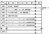
メモリMは、例えば、図2に示すように駆動手段Rによる動作の状況に対応させた速度及び加速度の制御条件をテーブルとして保持しており、本実施例では、速度及び加速度の制御条件を駆動手段Rの各軸毎に分けて保持している。
【0015】
例えば、駆動手段Rの加速度(減速度)を”速度1”として、駆動手段Rを通常移動させる際のイニシャル速度と、プロセスチャンバ内の異物を検出しながら基板を搬送するといった事象の第1調整速度とを”速度2”として、駆動手段Rの軸1〜軸4による動作を行う或る事象の速度と、駆動手段Rの軸5及び軸6による動作を行う或る事象の第2調整速度とを”速度3”として、基板保持手段Tが基板を保持していない場合の速度を”速度4”として、プロセスチャンバPC1に対しての動作において基板保持手段Tが基板を保持している際に基板のずれを生じさせることのない搬送速度を”速度5”として、プロセスチャンバPC2に対しての動作において基板保持手段Tが基板を保持している際に基板のずれを生じさせることのない搬送速度を”速度6”として、プロセスチャンバPC2に対しての動作において基板保持手段Tが基板を保持している際に基板のずれを生じさせることのない搬送速度を”速度7”として保持している。
ここで、基板を保持していない場合の速度”速度4”としては、基板を保持している場合の速度”速度5”、”速度6”及び”速度7”よりも速いものを設定している。
【0016】
なお、複数の事象であっても速度が同一の場合には、上記した”速度2”のように同一のエントリにまとめることによって、メモリMの記憶効率を向上させることができる。また、或る事象において動作する軸と、他の或る事象において動作する軸とが重ならない場合には、上記した”速度3”のように同一のエントリにまとめることによってメモリMの記憶効率を向上することができる。
【0017】
なお、図2に示すテーブルをディスプレイ装置等の表示装置(図示せず)に表示させておき、キーボード等の入力手段(図示せず)からオペレータがメモリMへ情報を設定できるようにすることもできる。
【0018】
駆動制御手段Cは、駆動手段Rを動作させる状況に応じて、メモリMから当該状況に対応する速度及び加速度を取り出し、取り出した速度及び加速度に従って駆動手段Rの各軸を制御する。
例えば、プロセスチャンバPC1に対して基板を搬入する場合においては、メモリMから”速度1”及び”速度5”を取り出し、当該取り出した”速度1”を搬送加速度とし、”速度5”を搬送速度として、駆動手段Rの各軸を制御する。
【0019】
次に、上記した基板搬送装置Kの動作をプロセスチャンバPC1に載置されている基板をプロセスチャンバPC3に搬送する場合を例にとって説明する。
まず、駆動制御手段CがメモリMから基板不保持速度”速度4”と、加速度”速度1”を取り出し、当該”速度4”及び”速度1”に従って、駆動手段Rを回転及び伸長させて基板を保持していない基板保持手段TをプロセスチャンバPC1内に移動させ、所定の基板載置位置の基板を基板保持手段Tに載置させる。次いで、駆動制御手段Cは、メモリMからプロセスチャンバPC1に対する基板の搬送速度”速度5”を取り出し、当該”速度5”及び”速度1”に従って、駆動手段Rを収縮させて、基板保持手段TをプロセスチャンバPC1外に移動させる。
【0020】
次に、駆動制御手段CがメモリMからプロセスチャンバPC3に対する基板搬送速度”速度7”を取り出し、当該”速度7”及び”速度1”に従って、駆動手段Rを回転及び伸長させて基板保持手段TをプロセスチャンバPC3内に移動させ、所定の基板載置位置に基板保持手段Tが保持する基板を載置させる。次いで、駆動制御手段Cは、メモリMから基板不保持速度”速度4”を取り出し、当該”速度4”及び”速度1”に従って、駆動手段Rを収縮させて、基板保持手段TをプロセスチャンバPC3外に移動させる。
【0021】
このように、各チャンバに対する駆動手段Rによる動作時に、基板保持手段Tが基板を保持している場合には、基板のずれを生じさせない各チャンバ毎の搬送速度に従って基板の搬送が行われるために、基板のずれが発生することを防止できる。また、各チャンバ毎の搬送速度を基板のずれが発生しない範囲で速くすればするほど、搬送処理時間を短縮することができる。
また、基板を搬送していない場合には基板を保持している場合よりも速度を速くしたために、搬送処理の時間をさらに短縮することができる。
【0022】
なお、例えば、高温処理を行うプロセスチャンバに対して搬送処理を行う場合には、搬送処理の時間を短縮することができるために、搬送処理中に当該チャンバから奪われる熱量を抑えることができ、当該チャンバに対する温度制御を容易にすることができる。
【0023】
なお、上記した実施例では、いずれのチャンバに対する搬送処理においても搬送加速度を同一にしていたが、各チャンバ毎に搬送加速度を設定するようにすれば、より効果的に各チャンバに対する搬送処理での基板のずれを防ぐとともに、搬送処理の時間を短縮することができる。
また、基板を保持していない場合の加速度は、基板を保持している場合の搬送加速度よりも大きくすることができるので、基板を保持していない場合の加速度を基板を保持している場合より大きく設定しておけば、搬送処理の時間をより短縮することができる。
【0024】
なお、上記した実施例では、基板を保持していない場合の速度を、基板を保持している場合の搬送速度より速くすることによって、搬送処理時間をより効果的に短縮していたが、基板を保持しているか否かに関わらず速度を同一として、各チャンバ毎に設定した場合においても、搬送処理の時間を短縮することができる。
【0025】
なお、上記した実施例では、各チャンバ毎に設定された搬送速度及び搬送加速度の両方の制御条件に基づいて、駆動手段を制御するようにしていたが、各チャンバ毎に搬送加速度のみの制御条件を設定し、当該制御条件に基づいて制御を行うようにしてもよく、要は、各チャンバ毎に設定された搬送速度及び搬送加速度の少なくとも一方の制御条件に基づいて制御を行えばよい。
【0026】
【発明の効果】
以上説明したように、本発明に係る基板搬送装置では、各チャンバ毎に搬送速度及び搬送加速度の少なくとも一方の制御条件を設定し、当該制御条件に基づいて、基板の搬送を行うようにしたために、各チャンバに対する搬送処理において、基板のずれが発生するといった事態を防ぐことができるとともに、搬送処理に要する時間を短縮することができる。
【図面の簡単な説明】
【図1】 本発明の一実施例に係る基板搬送装置を備えた半導体製造装置の一部分の構成図である。
【図2】 本発明の一実施例に係る駆動手段を制御する速度及び加速度の制御条件を説明する図である。
【図3】 従来例に係る基板搬送装置を備えた半導体製造装置の一部分の構成図である。
【符号の説明】
PC1、PC2、PC3・・プロセスチャンバ、
J、K・・基板搬送装置、
T・・基板保持手段、
R・・駆動手段、
C・・駆動制御手段、
M・・メモリ、[0001]
BACKGROUND OF THE INVENTION
The present invention relates to a substrate transfer apparatus that performs transfer processing of a substrate to a plurality of chambers in a semiconductor manufacturing apparatus including a plurality of chambers.
[0002]
[Prior art]
A semiconductor manufacturing apparatus includes a plurality of chambers for performing a plurality of predetermined processes on a substrate to be processed such as a semiconductor wafer and a glass substrate, and the substrate transfer apparatus performs a substrate transfer process between the chambers. There is something to make.
Such a semiconductor manufacturing apparatus will be described with reference to a part of the apparatus shown in FIG.
The semiconductor manufacturing apparatus includes process chambers PC1 to PC3 that perform predetermined processing on a substrate, and a substrate transfer device J that performs transfer processing of the substrate between the chambers.
[0003]
The process chambers PC1 to PC3 are chambers that perform different processes, and the shapes of the chambers are different.
The substrate transfer device J includes a substrate holding means T for placing and holding a substrate, and a driving means R for moving the substrate holding means T by performing rotation and expansion / contraction operations. The processing is performed based on the same preset conveyance speed and conveyance acceleration.
[0004]
For example, when a substrate is carried into the process chamber PC1, the driving means R moves the substrate holding means T on which the substrate is placed and held into the process chamber PC1 by the rotation and extension operations based on the setting, and a predetermined substrate is obtained. The substrate held by the substrate holding means T is placed at the placement position. Next, the driving means R moves the substrate holding means T out of the process chamber PC1 by a contraction operation based on the setting.
[0005]
On the other hand, when the substrate is unloaded from the process chamber PC1, the driving means R is moved into the process chamber PC1 by the rotation and extension operations based on the setting, and the substrate at a predetermined substrate placement position is transferred to the substrate holding means T. Place. Next, the driving means R moves the substrate holding means T, on which the substrate is placed and held, to the outside of the process chamber PC1 by the contraction operation based on the setting.
Then, the substrate is transported based on the same transport speed and transport acceleration set in advance for the other chambers.
When the drive device R is configured by a plurality of mechanisms (axes), the speed and acceleration for each axis may be set as the above-described transport speed and transport acceleration.
[0006]
In the invention described in Japanese Patent Laid-Open No. 7-307373, the processing efficiency of the transfer process is improved by changing the speed and acceleration depending on whether or not the wafer is held in the transfer process of the wafer (substrate). Is described.
[0007]
[Problems to be solved by the invention]
In semiconductor manufacturing equipment, it is desired to improve processing efficiency by shortening the time required for substrate transport processing. For this reason, in the above-described substrate transport device, the transport speed is increased and the transport acceleration is increased. Has been done.
[0008]
However, in the above-described conventional substrate transfer apparatus, the longer the extension length of the drive device, the greater the vibration applied to the substrate holding means, and the more the transfer speed is increased or the transfer acceleration is increased, the more the vibration is applied to the substrate holding means substrate. The transport speed and transport acceleration when the substrate holding means is holding the substrate are different from each other in the transport processing for the chamber that requires the longest extension operation by the driving device. In addition, it must be possible to prevent a situation such as dropping off the substrate, and there is a limit to shortening the time.
[0009]
Therefore, the present invention has been made in view of the conventional circumstances, and an object of the present invention is to provide a substrate transfer apparatus that can prevent the substrate from being displaced in the transfer process and can further improve the processing efficiency of the substrate transfer process. .
[0010]
[Means for Solving the Problems]
In order to achieve the above-described object, the present invention was made paying attention to the fact that the conveyance speed and the acceleration at which the substrate is displaced may be different for each chamber to be conveyed. At least one control condition of transport speed and transport acceleration is set, and transport processing for each chamber is performed based on the control condition.
[0011]
A substrate transfer apparatus according to the present invention is a substrate transfer apparatus for transferring a substrate to a plurality of chambers, a substrate holding means for holding and transferring a substrate, and a substrate holding means for moving the substrate relative to the chamber. A drive means for carrying, a drive control means for controlling the movement of the substrate holding means by the drive means for each chamber, based on the control conditions of at least one of the carry speed and the carry acceleration set for each chamber; It is provided with.
[0012]
In the substrate transport apparatus described above, the drive control unit controls the movement of the substrate holding unit by the drive unit based on the control condition of at least one of the transport speed and the transport acceleration set for each chamber, and transports the substrate to the chamber. Let it be done.
Therefore, by setting at least one control condition of the conveyance speed and the conveyance acceleration that does not cause the substrate displacement for each chamber, the occurrence of the substrate displacement can be prevented.
In addition, the time required for the transfer process can be shortened by setting the transfer speed to be high and the transfer acceleration to be large within a range where the substrate does not shift for each chamber.
[0013]
DETAILED DESCRIPTION OF THE INVENTION
A part of a semiconductor manufacturing apparatus including a substrate transfer apparatus according to an embodiment of the present invention will be described with reference to FIG. In addition, the same number is attached | subjected to the part same as a prior art example.
The substrate transfer device K includes a substrate holding means T for placing and holding a substrate, a driving means R for moving the substrate holding means T, a memory M for holding speed and acceleration control conditions that define the operation of the driving means R, and Drive control means C for controlling the drive means R based on the control conditions of the memory M.
[0014]
The driving means R has a configuration including a plurality of shafts, and the substrate holding means T is moved by performing operations such as expansion, contraction, and rotation by the operation of each shaft.
For example, as shown in FIG. 2, the memory M holds a speed and acceleration control condition corresponding to the state of operation by the driving means R as a table. In this embodiment, the memory M drives the speed and acceleration control condition. The means R is held separately for each axis.
[0015]
For example, when the acceleration (deceleration) of the driving means R is “speed 1”, the initial adjustment when the driving means R is normally moved, and the first adjustment of the event of transporting the substrate while detecting foreign matter in the process chamber Speed is “speed 2”, the speed of a certain event in which the operation of the driving means R by the axes 1 to 4 is performed, and the second adjustment speed of a certain event in which the movement of the driving means R by the axes 5 and 6 is performed. And “speed 3”, the speed when the substrate holding means T is not holding the substrate is “speed 4”, and the substrate holding means T is holding the substrate in the operation with respect to the process chamber PC1. In this operation, the substrate holding means T holds the substrate in the operation with respect to the process chamber PC2 with the conveyance speed that does not cause the substrate being shifted as "speed 5". The feeding speed is set to “speed 6”, and the transport speed that does not cause the displacement of the substrate when the substrate holding means T holds the substrate in the operation with respect to the process chamber PC2 is held as “speed 7”. ing.
Here, the speed “speed 4” when the substrate is not held is set to be higher than the speeds “speed 5”, “speed 6”, and “speed 7” when the substrate is held. Yes.
[0016]
If the speed is the same even for a plurality of events, the storage efficiency of the memory M can be improved by grouping them into the same entry as in “speed 2” described above. Further, when the axis that operates in a certain event and the axis that operates in another certain event do not overlap, the storage efficiency of the memory M is improved by grouping them into the same entry as in the above “speed 3”. Can be improved.
[0017]
The table shown in FIG. 2 may be displayed on a display device (not shown) such as a display device so that the operator can set information in the memory M from an input means (not shown) such as a keyboard. it can.
[0018]
The drive control means C takes out the speed and acceleration corresponding to the situation from the memory M according to the situation in which the drive means R is operated, and controls each axis of the drive means R according to the taken out speed and acceleration.
For example, when the substrate is carried into the process chamber PC1, “speed 1” and “speed 5” are taken out from the memory M, and the “speed 1” thus taken is taken as the carrying acceleration, and “speed 5” is taken as the carrying speed. As described above, each axis of the driving means R is controlled.
[0019]
Next, the operation of the substrate transfer apparatus K described above will be described by taking as an example a case where a substrate placed in the process chamber PC1 is transferred to the process chamber PC3.
First, the drive control means C takes out the substrate non-holding speed “speed 4” and the acceleration “speed 1” from the memory M, and rotates and expands the drive means R according to the “speed 4” and “speed 1” to obtain the substrate. The substrate holding means T not holding the substrate is moved into the process chamber PC1, and the substrate at a predetermined substrate placement position is placed on the substrate holding means T. Next, the drive control means C takes out the substrate transport speed “speed 5” from the memory M to the process chamber PC1, and contracts the drive means R in accordance with the “speed 5” and “speed 1” to thereby provide the substrate holding means T. Is moved out of the process chamber PC1.
[0020]
Next, the drive control means C takes out the substrate transfer speed “speed 7” for the process chamber PC3 from the memory M, and rotates and expands the drive means R according to the “speed 7” and “speed 1” to thereby provide the substrate holding means T. Is moved into the process chamber PC3, and the substrate held by the substrate holding means T is placed at a predetermined substrate placement position. Next, the drive control means C takes out the substrate non-holding speed “speed 4” from the memory M, and contracts the driving means R in accordance with the “speed 4” and “speed 1”, thereby bringing the substrate holding means T into the process chamber PC3. Move outside.
[0021]
Thus, when the substrate holding means T holds the substrate during the operation by the driving means R for each chamber, the substrate is transferred according to the transfer speed for each chamber that does not cause the substrate to shift. It is possible to prevent the substrate from being displaced. In addition, as the transfer speed for each chamber is increased within a range in which the substrate does not shift, the transfer processing time can be shortened.
In addition, since the speed is increased when the substrate is not transported compared to when the substrate is held, the time for the transport process can be further shortened.
[0022]
In addition, for example, when carrying out a transfer process for a process chamber that performs a high-temperature process, since the time for the transfer process can be shortened, the amount of heat taken away from the chamber during the transfer process can be suppressed, Temperature control for the chamber can be facilitated.
[0023]
In the above-described embodiment, the transfer acceleration is the same in the transfer process for any chamber. However, if the transfer acceleration is set for each chamber, the transfer process for each chamber can be more effectively performed. It is possible to prevent the substrate from being displaced and to shorten the time for carrying processing.
In addition, the acceleration when the substrate is not held can be larger than the conveyance acceleration when the substrate is held, so the acceleration when the substrate is not held is higher than when the substrate is held. If it is set to a large value, it is possible to further shorten the time for carrying processing.
[0024]
In the above-described embodiment, the transfer processing time is more effectively shortened by making the speed when the substrate is not held faster than the transfer speed when the substrate is held. Even when the same speed is set for each chamber regardless of whether or not it is held, the time for the transfer process can be shortened.
[0025]
In the above-described embodiment, the driving unit is controlled based on the control conditions for both the transport speed and the transport acceleration set for each chamber. However, the control condition for only the transport acceleration is set for each chamber. And the control may be performed based on the control condition. In short, the control may be performed based on the control condition of at least one of the transport speed and the transport acceleration set for each chamber.
[0026]
【The invention's effect】
As described above, in the substrate transfer apparatus according to the present invention, at least one control condition of transfer speed and transfer acceleration is set for each chamber, and the substrate is transferred based on the control condition. In the transfer process for each chamber, it is possible to prevent a situation in which the substrate is displaced, and to shorten the time required for the transfer process.
[Brief description of the drawings]
FIG. 1 is a partial configuration diagram of a semiconductor manufacturing apparatus including a substrate transfer apparatus according to an embodiment of the present invention.
FIG. 2 is a diagram illustrating speed and acceleration control conditions for controlling a driving unit according to an embodiment of the present invention.
FIG. 3 is a partial configuration diagram of a semiconductor manufacturing apparatus including a substrate transfer apparatus according to a conventional example.
[Explanation of symbols]
PC1, PC2, PC3 ... Process chamber,
J, K ... substrate transfer device,
T. ・ Substrate holding means,
R ... Drive means,
C ... Drive control means
M ... memory
Claims (1)
基板を保持して搬送を行う基板保持手段と、
基板保持手段を移動させてチャンバに対する基板の搬送を行わせる駆動手段と、
各チャンバ毎に設定された複数の搬送速度及び搬送加速度を保持するメモリと、
チャンバに対して搬送処理を行うに際して前記メモリに保持された搬送速度と搬送加速度とを選択し、当該選択した搬送速度と搬送加速度とに従って当該チャンバに対する駆動手段による基板保持手段の移動を制御する駆動制御手段と、を備えたことを特徴とする基板搬送装置。In a substrate transfer apparatus that performs substrate transfer processing for a plurality of chambers,
A substrate holding means for holding and transferring the substrate;
Driving means for moving the substrate holding means to carry the substrate to the chamber;
A memory for holding a plurality of transfer speeds and transfer accelerations set for each chamber;
Driving for controlling the movement of the substrate holding means by the driving means with respect to the chamber in accordance with the selected conveying speed and the conveying acceleration in accordance with the selected conveying speed and the conveying acceleration when performing the carrying process on the chamber. And a control means.
Priority Applications (1)
| Application Number | Priority Date | Filing Date | Title |
|---|---|---|---|
| JP35408796A JP3934191B2 (en) | 1996-12-18 | 1996-12-18 | Semiconductor manufacturing equipment |
Applications Claiming Priority (1)
| Application Number | Priority Date | Filing Date | Title |
|---|---|---|---|
| JP35408796A JP3934191B2 (en) | 1996-12-18 | 1996-12-18 | Semiconductor manufacturing equipment |
Publications (2)
| Publication Number | Publication Date |
|---|---|
| JPH10178083A JPH10178083A (en) | 1998-06-30 |
| JP3934191B2 true JP3934191B2 (en) | 2007-06-20 |
Family
ID=18435208
Family Applications (1)
| Application Number | Title | Priority Date | Filing Date |
|---|---|---|---|
| JP35408796A Expired - Lifetime JP3934191B2 (en) | 1996-12-18 | 1996-12-18 | Semiconductor manufacturing equipment |
Country Status (1)
| Country | Link |
|---|---|
| JP (1) | JP3934191B2 (en) |
Families Citing this family (7)
| Publication number | Priority date | Publication date | Assignee | Title |
|---|---|---|---|---|
| US6977014B1 (en) | 2000-06-02 | 2005-12-20 | Novellus Systems, Inc. | Architecture for high throughput semiconductor processing applications |
| US6712907B1 (en) * | 2000-06-23 | 2004-03-30 | Novellus Systems, Inc. | Magnetically coupled linear servo-drive mechanism |
| US6860965B1 (en) | 2000-06-23 | 2005-03-01 | Novellus Systems, Inc. | High throughput architecture for semiconductor processing |
| JP4841183B2 (en) * | 2005-06-28 | 2011-12-21 | 東京エレクトロン株式会社 | Substrate processing apparatus, transfer apparatus, and control method of transfer apparatus |
| US7286890B2 (en) | 2005-06-28 | 2007-10-23 | Tokyo Electron Limited | Transfer apparatus for target object |
| JP5675416B2 (en) * | 2011-02-17 | 2015-02-25 | 東京エレクトロン株式会社 | Method for conveying object to be processed and apparatus for processing object to be processed |
| JP2020017645A (en) | 2018-07-26 | 2020-01-30 | 株式会社Kokusai Electric | Substrate processing apparatus |
-
1996
- 1996-12-18 JP JP35408796A patent/JP3934191B2/en not_active Expired - Lifetime
Also Published As
| Publication number | Publication date |
|---|---|
| JPH10178083A (en) | 1998-06-30 |
Similar Documents
| Publication | Publication Date | Title |
|---|---|---|
| JP4087328B2 (en) | Coating and developing apparatus and operating method of coating and developing apparatus | |
| JP3934191B2 (en) | Semiconductor manufacturing equipment | |
| JPH0722490A (en) | Device and method for automatically arranging lots | |
| US7392812B2 (en) | Substrate processing apparatus and substrate transporting device mounted thereto | |
| JP4541966B2 (en) | Coating processing method, coating processing apparatus, and computer program | |
| JP6049394B2 (en) | Substrate processing system and substrate transfer control method | |
| JPH10199960A (en) | Method for controlling conveyance of substrate of semiconductor manufacturing apparatus | |
| KR100188453B1 (en) | Transportation-transfer device for an object of treatment | |
| JP2011091334A (en) | Substrate treatment apparatus | |
| JP4018965B2 (en) | Substrate processing equipment | |
| JPH08222618A (en) | Method and apparatus for conveying | |
| US4888994A (en) | Method of carrying objects into and from a furnace, and apparatus for carrying objects into and from a furnace | |
| JP2002237507A (en) | Processing system, and method for conveying element to be processed of the processing system | |
| JP2002246443A (en) | Substrate transfer control method and device therefor | |
| JP2960181B2 (en) | Processing equipment | |
| JP4496073B2 (en) | Substrate processing apparatus and substrate processing method | |
| JPH10247679A (en) | Semiconductor treating device | |
| JP2719524B2 (en) | Semiconductor manufacturing equipment | |
| JPH11135598A (en) | Substrate carrying system | |
| JP2001044119A (en) | Resist coating, developing, and processing apparatus | |
| JPH0329317A (en) | Arrangement apparatus for semiconductor wafer | |
| JP3325834B2 (en) | Heat treatment apparatus and heat treatment method | |
| JP2889938B2 (en) | Wafer carrier transfer device | |
| JPH08250571A (en) | Wafer conveying method | |
| JP2649822B2 (en) | Processing equipment |
Legal Events
| Date | Code | Title | Description |
|---|---|---|---|
| A977 | Report on retrieval |
Free format text: JAPANESE INTERMEDIATE CODE: A971007 Effective date: 20061127 |
|
| A131 | Notification of reasons for refusal |
Free format text: JAPANESE INTERMEDIATE CODE: A131 Effective date: 20061219 |
|
| A521 | Written amendment |
Free format text: JAPANESE INTERMEDIATE CODE: A523 Effective date: 20070216 |
|
| TRDD | Decision of grant or rejection written | ||
| A01 | Written decision to grant a patent or to grant a registration (utility model) |
Free format text: JAPANESE INTERMEDIATE CODE: A01 Effective date: 20070313 |
|
| A61 | First payment of annual fees (during grant procedure) |
Free format text: JAPANESE INTERMEDIATE CODE: A61 Effective date: 20070315 |
|
| R150 | Certificate of patent or registration of utility model |
Free format text: JAPANESE INTERMEDIATE CODE: R150 |
|
| FPAY | Renewal fee payment (event date is renewal date of database) |
Free format text: PAYMENT UNTIL: 20100330 Year of fee payment: 3 |
|
| FPAY | Renewal fee payment (event date is renewal date of database) |
Free format text: PAYMENT UNTIL: 20110330 Year of fee payment: 4 |
|
| FPAY | Renewal fee payment (event date is renewal date of database) |
Free format text: PAYMENT UNTIL: 20120330 Year of fee payment: 5 |
|
| FPAY | Renewal fee payment (event date is renewal date of database) |
Free format text: PAYMENT UNTIL: 20120330 Year of fee payment: 5 |
|
| FPAY | Renewal fee payment (event date is renewal date of database) |
Free format text: PAYMENT UNTIL: 20130330 Year of fee payment: 6 |
|
| FPAY | Renewal fee payment (event date is renewal date of database) |
Free format text: PAYMENT UNTIL: 20130330 Year of fee payment: 6 |
|
| FPAY | Renewal fee payment (event date is renewal date of database) |
Free format text: PAYMENT UNTIL: 20140330 Year of fee payment: 7 |
|
| EXPY | Cancellation because of completion of term |