JP3927953B2 - Amplitude conversion circuit - Google Patents
Amplitude conversion circuit Download PDFInfo
- Publication number
- JP3927953B2 JP3927953B2 JP2003572178A JP2003572178A JP3927953B2 JP 3927953 B2 JP3927953 B2 JP 3927953B2 JP 2003572178 A JP2003572178 A JP 2003572178A JP 2003572178 A JP2003572178 A JP 2003572178A JP 3927953 B2 JP3927953 B2 JP 3927953B2
- Authority
- JP
- Japan
- Prior art keywords
- electrode
- transistor
- signal
- voltage
- node
- Prior art date
- Legal status (The legal status is an assumption and is not a legal conclusion. Google has not performed a legal analysis and makes no representation as to the accuracy of the status listed.)
- Expired - Fee Related
Links
Images


Classifications
-
- G—PHYSICS
- G09—EDUCATION; CRYPTOGRAPHY; DISPLAY; ADVERTISING; SEALS
- G09G—ARRANGEMENTS OR CIRCUITS FOR CONTROL OF INDICATING DEVICES USING STATIC MEANS TO PRESENT VARIABLE INFORMATION
- G09G3/00—Control arrangements or circuits, of interest only in connection with visual indicators other than cathode-ray tubes
- G09G3/20—Control arrangements or circuits, of interest only in connection with visual indicators other than cathode-ray tubes for presentation of an assembly of a number of characters, e.g. a page, by composing the assembly by combination of individual elements arranged in a matrix no fixed position being assigned to or needed to be assigned to the individual characters or partial characters
- G09G3/34—Control arrangements or circuits, of interest only in connection with visual indicators other than cathode-ray tubes for presentation of an assembly of a number of characters, e.g. a page, by composing the assembly by combination of individual elements arranged in a matrix no fixed position being assigned to or needed to be assigned to the individual characters or partial characters by control of light from an independent source
- G09G3/36—Control arrangements or circuits, of interest only in connection with visual indicators other than cathode-ray tubes for presentation of an assembly of a number of characters, e.g. a page, by composing the assembly by combination of individual elements arranged in a matrix no fixed position being assigned to or needed to be assigned to the individual characters or partial characters by control of light from an independent source using liquid crystals
-
- H—ELECTRICITY
- H03—ELECTRONIC CIRCUITRY
- H03K—PULSE TECHNIQUE
- H03K3/00—Circuits for generating electric pulses; Monostable, bistable or multistable circuits
- H03K3/02—Generators characterised by the type of circuit or by the means used for producing pulses
- H03K3/353—Generators characterised by the type of circuit or by the means used for producing pulses by the use, as active elements, of field-effect transistors with internal or external positive feedback
- H03K3/356—Bistable circuits
- H03K3/356104—Bistable circuits using complementary field-effect transistors
- H03K3/356113—Bistable circuits using complementary field-effect transistors using additional transistors in the input circuit
-
- G—PHYSICS
- G09—EDUCATION; CRYPTOGRAPHY; DISPLAY; ADVERTISING; SEALS
- G09G—ARRANGEMENTS OR CIRCUITS FOR CONTROL OF INDICATING DEVICES USING STATIC MEANS TO PRESENT VARIABLE INFORMATION
- G09G2310/00—Command of the display device
- G09G2310/02—Addressing, scanning or driving the display screen or processing steps related thereto
- G09G2310/0264—Details of driving circuits
- G09G2310/0289—Details of voltage level shifters arranged for use in a driving circuit
-
- H—ELECTRICITY
- H03—ELECTRONIC CIRCUITRY
- H03K—PULSE TECHNIQUE
- H03K17/00—Electronic switching or gating, i.e. not by contact-making and –breaking
- H03K17/06—Modifications for ensuring a fully conducting state
- H03K17/063—Modifications for ensuring a fully conducting state in field-effect transistor switches
Landscapes
- Engineering & Computer Science (AREA)
- Chemical & Material Sciences (AREA)
- Crystallography & Structural Chemistry (AREA)
- Physics & Mathematics (AREA)
- Computer Hardware Design (AREA)
- General Physics & Mathematics (AREA)
- Theoretical Computer Science (AREA)
- Logic Circuits (AREA)
- Control Of Indicators Other Than Cathode Ray Tubes (AREA)
Description
【0001】
【発明の属する技術分野】
この発明は振幅変換回路に関し、特に、信号の振幅を変換するための振幅変換回路に関する。
【0002】
【従来の技術】
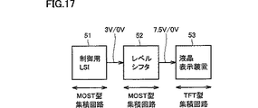
図17は、従来の携帯電話機の画像表示に関連する部分の構成を示すブロック図である。
【0003】
図17において、この携帯電話機は、MOST(MOSトランジスタ)型集積回路である制御用LSI51と、MOST型集積回路であるレベルシフタ52と、TFT(薄膜トランジスタ)型集積回路である液晶表示装置53とを備える。
【0004】
制御用LSI51は、液晶表示装置53用の制御信号を生成する。この制御信号の「H」レベルは3Vであり、その「L」レベルは0Vである。制御信号は実際には多数生成されるが、ここでは説明の簡単化のため制御信号は1つとする。レベルシフタ52は、制御用LSI51からの制御信号の論理レベルを変換して内部制御信号を生成する。この内部制御信号の「H」レベルは7.5Vであり、その「L」レベルは0Vである。液晶表示装置53は、レベルシフタ52からの内部制御信号に従って画像を表示する。
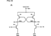
【0005】
図18は、レベルシフタ52の構成を示す回路図である。図18において、このレベルシフタ52は、PチャネルMOSトランジスタ54,55およびNチャネルMOSトランジスタ56,57を含む。PチャネルMOSトランジスタ54,55は、それぞれ電源電位VCC(7.5V)のノードN51と出力ノードN54,N55との間に接続され、それらのゲートはそれぞれ出力ノードN55,N54に接続される。NチャネルMOSトランジスタ56,57は、それぞれ出力ノードN54,N55と接地電位GNDのノードとの間に接続され、それらのゲートはそれぞれ入力信号VI,/VIを受ける。
【0006】
今、入力信号VI,/VIがそれぞれ「L」レベル(0V)および「H」レベル(3V)にされ、出力信号VO,/VOがそれぞれ「H」レベル(7.5V)および「L」レベル(0V)にされているものとする。このとき、MOSトランジスタ54,57が導通し、MOSトランジスタ55,56が非導通になっている。
【0007】
この状態で、入力信号VIが「L」レベル(0V)から「H」レベル(3V)に立上げられるとともに入力信号/VIが「H」レベル(3V)から「L」レベル(0V)に立下げられると、まずNチャネルMOSトランジスタ56が導通して出力ノードN54の電位が低下する。出力ノードN54の電位が、電源電位VCCからPチャネルMOSトランジスタ55のしきい値電圧の絶対値を減算した電位よりも低くなると、PチャネルMOSトランジスタ55が導通し始め、出力ノードN55の電位が上昇し始める。出力ノードN55の電位が上昇し始めると、PチャネルMOSトランジスタ54のソース−ゲート間の電圧が小さくなってPチャネルMOSトランジスタ54の導通抵抗値が高くなり、出力ノードN54の電位がさらに低下する。したがって、回路は正帰還的に動作し、出力ノードVO,/VOがそれぞれ「L」レベル(0V)および「H」レベル(7.5V)になってレベル変換動作が完了する。
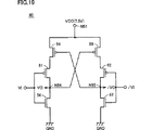
【0008】
図19は、従来の他のレベルシフタ60の構成を示す回路図である。図19を参照して、このレベルシフタ60が図18のレベルシフタ52と異なる点は、PチャネルMOSトランジスタ61,62が追加されている点である。PチャネルMOSトランジスタ61は、PチャネルMOSトランジスタ54のドレインと出力ノードN54との間に介挿され、そのゲートは入力信号VIを受ける。PチャネルMOSトランジスタ62は、PチャネルMOSトランジスタ55のドレインと出力ノードN55との間に介挿され、そのゲートは入力信号/VIを受ける。
【0009】
このレベルシフタ60では、入力信号VIが「L」レベル(0V)から「H」レベル(3V)に立上げられると、PチャネルMOSトランジスタ61が導通状態から非導通状態になり、電源電位VCCのノードN51から出力ノードN54に流れる電流が低減されるので、出力ノードN54の電位が低下しやすくなる。この結果、PチャネルMOSトランジスタ55が導通して出力ノードN55の電位が上昇しやすくなるので、図18のレベルシフタ52よりも動作マージンが大きくなる。
【0010】
このように、従来のレベルシフタ52,60では、入力信号VIが「L」レベル(0V)から「H」レベル(3V)に立上げられたことに応じてNチャネルMOSトランジスタ56が導通することが動作の前提となる。NチャネルMOSトランジスタ56が導通するためには、NチャネルMOSトランジスタ56のしきい値電位が入力信号VIの「H」レベル(3V)以下である必要がある。
【0011】
一般的な半導体LSIではトランジスタのしきい値電圧を3V以下にすることは容易であるが、液晶表示装置に含まれている低温ポリシリコンTFTはしきい値電圧のばらつきが大きく、TFTのしきい値電圧を3V以下にすることは困難である。このため、図17で示したように、高耐圧のMOSトランジスタで構成されたレベルシフタ52または60を制御用LSI51と液晶表示装置53との間に設けて信号の論理レベルの変換を行なっている。
【0012】
【発明が解決しようとする課題】
しかし、このようなレベルシフタ52,60を設けると、レベルシフタ52,60のコストがシステムコストに加算されることになり、システムコストの上昇を招く。
【0013】
それゆえに、この発明の主たる目的は、入力トランジスタのしきい値電圧よりも入力信号の振幅電圧が低い場合でも正常に動作する振幅変換回路を提供することである。
【0014】
【課題を解決するための手段および効果】
この発明に係る振幅変換回路は、その振幅が第1の電圧である第1の信号を、その振幅が第1の電圧よりも高い第2の電圧である第2の信号に変換するものである。この振幅変換回路では、それらの第1の電極がともに第2の電圧を受け、それらの第2の電極が第2の信号およびその相補信号を出力するための第1および第2の出力ノードにそれぞれ接続され、それらの入力電極がそれぞれ第2および第1の出力ノードに接続された第1の導電形式の第1および第2のトランジスタと、それらの第1の電極がそれぞれ第1および第2の出力ノードに接続された第2の導電形式の第3および第4のトランジスタと、第1の信号およびその相補信号によって駆動され、第1の信号の前縁に応答して第1の電圧よりも高い第3の電圧を第3のトランジスタの入力電極および第2の電極間に与えて第3のトランジスタを導通させ、第1の信号の後縁に応答して第3の電圧を第4のトランジスタの入力電極および第2の電極間に与えて第4のトランジスタを導通させる駆動回路とが設けられる。
【0015】
この駆動回路は、第3のトランジスタの入力電極および第2の電極間に接続された第1の抵抗素子と、その一方電極が第1の信号の相補信号を受け、その他方電極が第3のトランジスタの入力電極に接続された第1のキャパシタと、第4のトランジスタの入力電極および第2の電極間に接続された第2の抵抗素子と、その一方電極が第1の信号を受け、その他方電極が第4のトランジスタの入力電極に接続された第2のキャパシタとを含み、第1の信号およびその相補信号をそれぞれ第3および第4のトランジスタの第2の電極に与える。したがって、第1の信号の前縁または後縁に応答して第1の信号の振幅電圧である第1の電圧よりも高い第3の電圧を第3または第4のトランジスタの入力電極および第2の電極間に与えるので、第1の信号の振幅電圧が第3および第4のトランジスタのしきい値電圧よりも低い場合でも動作する。
【0016】
また好ましくは、第1の抵抗素子は、第3のトランジスタの入力電極および第2の電極間に接続され、その入力電極が第4の電圧を受ける第5のトランジスタを含む。第2の抵抗素子は、第4のトランジスタの入力電極および第2の電極間に接続され、その入力電極が第4の電圧を受ける第6のトランジスタを含む。この場合は、第1および第2の抵抗素子の占有面積が小さくて済む。
【0017】
また好ましくは、第5および第6のトランジスタは第2の導電形式であり、第4の電圧は第2の電圧に等しい。この場合は、電圧源の数が少なくて済む。
【0018】
また好ましくは、第1の抵抗素子は、第3のトランジスタの入力電極および第2の電極間に接続された第5のトランジスタを含む。第2の抵抗素子は、第4のトランジスタの入力電極および第2の電極間に接続された第6のトランジスタを含む。駆動回路は、さらに、第1の信号の前縁に応答して第5のトランジスタの抵抗値をパルス的に高くし、第1の信号の後縁に応答して第6のトランジスタの抵抗値をパルス的に高くするためのパルス発生回路を含む。この場合は、第3および第4のトランジスタの入力電極の電位低下を緩やかにすることができる。
【0019】
また好ましくは、第5および第6のトランジスタは第2の導電形式である。パルス発生回路は、第2の電圧と同極性の第4の電圧のノードと第5のトランジスタの入力電極との間に接続された第3の抵抗素子と、その一方電極が第1の信号を受け、その他方電極が第5のトランジスタの入力電極に接続された第3のキャパシタと、第4の電圧のノードと第6のトランジスタの入力電極との間に接続された第4の抵抗素子と、その一方電極が第1の信号の相補信号を受け、その他方電極が第6のトランジスタの入力電極に接続された第4のキャパシタとを含む。この場合は、第3または第4の抵抗素子を介して第4の電圧に充電された第5または第6のトランジスタの入力電極が第3または第4のキャパシタを介して第1の電圧分だけ降圧される。
【0020】
また好ましくは、第4の電圧は第2の電圧に等しい。この場合は、電圧源の数が少なくて済む。
【0021】
また好ましくは、第5および第6のトランジスタは第1の導電形式である。パルス発生回路は、第2の電圧と逆極性の第4の電圧のノードと第5のトランジスタの入力電極との間に接続された第3の抵抗素子と、その一方電極が第1の信号の相補信号を受け、その他方電極が第5のトランジスタの入力電極に接続された第3のキャパシタと、第4の電圧のノードと第6のトランジスタの入力電極との間に接続された第4の抵抗素子と、その一方電極が第1の信号を受け、その他方電極が第6のトランジスタの入力電極に接続された第4のキャパシタとを含む。この場合は、第3または第4の抵抗素子を介して第4の電圧に充電された第5または第6のトランジスタの入力電極が第3または第4のキャパシタを介して第1の電圧分だけ昇圧される。
【0022】
また好ましくは、駆動回路は、さらに、第3のトランジスタの第2の電極および入力電極間に接続された第1のダイオード素子と、第4のトランジスタの第2の電極および入力電極間に接続された第2のダイオード素子とを含む。この場合は、第3または第4のトランジスタの入力電極を第1の電圧に迅速に充電することができる。
【0023】
また、この発明に係る他の振幅変換回路は、その振幅が第1の電圧である第1の信号を、その振幅が第1の電圧よりも高い第2の電圧である第2の信号に変換するものである。この振幅変換回路では、それらの第1の電極がともに第2の電圧を受け、それらの第2の電極が第2の信号およびその相補信号を出力するための第1および第2の出力ノードにそれぞれ接続され、それらの入力電極がそれぞれ第2および第1の出力ノードに接続された第1の導電形式の第1および第2のトランジスタと、それらの第1の電極がそれぞれ第1および第2の出力ノードに接続された第2の導電形式の第3および第4のトランジスタと、第1の信号およびその相補信号によって駆動され、第1の信号の前縁に応答して第1の電圧よりも高い第3の電圧を第3のトランジスタの入力電極および第2の電極間に与えて第3のトランジスタを導通させ、第1の信号の後縁に応答して第3の電圧を第4のトランジスタの入力電極および第2の電極間に与えて第4のトランジスタを導通させる駆動回路とが設けられる。この駆動回路は、第3のトランジスタの第2の電極と基準電圧のノードとの間に接続された第1の抵抗素子と、その一方電極が第1の信号を受け、その他方電極が第3のトランジスタの第2の電極に接続された第1のキャパシタと、第4のトランジスタの第2の電極と基準電圧のノードとの間に接続された第2の抵抗素子と、その一方電極が第1の信号の相補信号を受け、その他方電極が第4のトランジスタの第2の電極に接続された第2のキャパシタとを含み、第1の信号およびその相補信号をそれぞれ第4および第3のトランジスタの入力電極に与える。したがって、第1の信号の前縁または後縁に応答して第1の信号の振幅電圧である第1の電圧よりも高い第3の電圧を第3または第4のトランジスタの入力電極および第2の電極間に与えるので、第1の信号の振幅電圧が第3および第4のトランジスタのしきい値電圧よりも低い場合でも動作する。
【0024】
また好ましくは、第1の抵抗素子は、第3のトランジスタの第2の電極と基準電圧のノードとの間に接続された第5のトランジスタを含む。第2の抵抗素子は、第2のトランジスタの第2の電極と基準電圧のノードとの間に接続された第6のトランジスタを含む。駆動回路は、さらに、第1の信号の前縁に応答して第5のトランジスタの抵抗値をパルス的に高くし、第1の信号の後縁に応答して第6のトランジスタの抵抗値をパルス的に高くするためのパルス発生回路を含む。この場合は、第3および第4のトランジスタの入力電極の電圧上昇を緩やかにすることができる。
【0025】
また好ましくは、第5および第6のトランジスタは第2の導電形式である。パルス発生回路は、第2の電圧と同極性の第4の電圧のノードと第5のトランジスタの入力電極との間に接続された第3の抵抗素子と、その一方電極が第1の信号を受け、その他方電極が第5のトランジスタの入力電極に接続された第3のキャパシタと、第4の電圧のノードと第6のトランジスタの入力電極との間に接続された第4の抵抗素子と、その一方電極が第1の信号の相補信号を受け、その他方電極が第6のトランジスタの入力電極に接続された第4のキャパシタとを含む。この場合は、第3または第4の抵抗素子を介して第4の電圧に充電された第5または第6のトランジスタの入力電極が第3または第4のキャパシタを介して第1の電圧分だけ降圧される。
【0026】
また好ましくは、第4の電圧は第2の電圧に等しい。この場合は、電圧源の数が少なくて済む。
【0027】
また好ましくは、さらに、第1および第2の出力ノードの電位をラッチするためのラッチ回路が設けられる。この場合は、第1および第2の出力ノードの電位を安定に保持することができる。
【0028】
また好ましくは、ラッチ回路は、それらの第1の電極がそれぞれ第1および第2の出力ノードに接続され、それらの第2の電極がそれぞれ第1の信号およびその相補信号を受け、それらの入力電極がそれぞれ第2および第1の出力ノードに接続された第2の導電形式の第5および第6のトランジスタを含む。この場合は、ラッチ回路を容易に構成することができる。
【0029】
また好ましくは、ラッチ回路は、それぞれ第1および第2の出力ノードと基準電圧のノードとの間に接続され、それらの入力電極がそれぞれ第2および第1の出力ノードに接続された第2の導電形式の第5および第6のトランジスタを含む。この場合は、第1の信号およびその相補信号の駆動力が小さくて済む。
【0030】
また好ましくは、さらに、第1のトランジスタの第2の電極と第1の出力ノードとの間に介挿され、その入力電極が第3のトランジスタの入力電極に接続された第1の導電形式の第5のトランジスタと、第2のトランジスタの第2の電極と第2の出力ノードとの間に介挿され、その入力電極が第4のトランジスタの入力電極に接続された第1の導電形式の第6のトランジスタとが設けられる。この場合は、第2の電圧のノードから第1および第2の出力ノードに流れる電流を小さくすることができ、消費電流の低減化を図ることができる。
【0031】
また好ましくは、第1〜第4のトランジスタは薄膜トランジスタである。この発明は、この場合に特に有効である。
【0032】
【発明の実施の形態】
[実施の形態1]
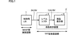
図1は、この発明の実施の形態1による携帯電話機の画像表示に関連する部分の構成を示すブロック図である。
【0033】
図1において、この携帯電話機は、MOST型集積回路である制御用LSI1と、TFT型集積回路である液晶表示装置2とを備え、液晶表示装置2はレベルシフタ3および液晶表示部4を含む。
【0034】
制御用LSI1は、液晶表示装置2用の制御信号を出力する。この制御信号の「H」レベルは3Vであり、その「L」レベルは0Vである。制御信号は実際には多数生成されるが、ここでは説明の簡単化のため制御信号は1つとする。レベルシフタ3は、制御用LSI1からの制御信号の論理レベルを変換して内部制御信号を生成する。この内部制御信号の「H」レベルは7.5Vであり、その「L」レベルは0Vである。液晶表示部4は、レベルシフタ3からの内部制御信号に従って画像を表示する。
【0035】
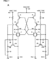
図2は、レベルシフタ3の構成を示す回路図である。図2において、このレベルシフタ3は、P型TFT5,6、N型TFT7〜10、抵抗素子11,12およびキャパシタ13,14を含む。P型TFT5,6は、それぞれ電源電位VCC(7.5V)のノードN1と出力ノードN5,N6との間に接続され、それらのゲートはそれぞれ出力ノードN6,N5に接続される。出力ノードN5,N6に現われる信号は、それぞれ、このレベルシフタ3の出力信号VO,/VOとなる。N型TFT7は、出力ノードN5と入力ノードN11との間に接続され、そのゲートは出力ノードN6に接続される。N型TFT8は、出力ノードN6と入力ノードN12との間に接続され、そのゲートは出力ノードN5に接続される。入力ノードN11,N12は、それぞれ入力信号VI,/VIを受ける。P型TFT5,6およびN型TFT7,8は、出力ノードN5,N6のレベルをラッチするためのラッチ回路を構成する。
【0036】
N型TFT9は、入力ノードN11と出力ノードN5との間に接続され、そのゲートはノードN9に接続される。N型TFT10は、入力ノードN11と出力ノードN6との間に接続され、そのゲートはノードN10に接続される。抵抗素子11はノードN9とN11の間に接続され、抵抗素子12はノードN10とN12の間に接続される。キャパシタ13は入力ノードN13とノードN9との間に接続され、キャパシタ14は入力ノードN14とノードN10との間に接続される。入力ノードN13,N14は、それぞれ入力信号/VI,VIを受ける。抵抗素子11およびキャパシタ13は昇圧回路を構成し、抵抗素子12およびキャパシタ14は昇圧回路を構成する。
【0037】
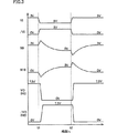
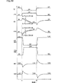
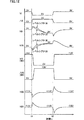
図3は、図2に示したレベルシフタ3の動作を示すタイムチャートである。図3を参照して、初期状態では、入力信号VI,/VIがそれぞれ「H」レベル(3V)および「L」レベル(0V)にされ、出力信号VO,/VOがそれぞれ「H」レベル(7.5V)および「L」レベル(0V)にされている。このとき、ノードN9は抵抗素子11によって入力信号VIと同電位の3Vにされ、ノードN10は抵抗素子12によって入力信号/VIと同電位の0Vにされている。これらの電位関係により、P型TFT5およびN型TFT8が導通し、他のTFT6,7,9,10は非導通になっている。つまり、出力ノードN5はP型TFT5を介して電源電位VCC(7.5V)を受け、出力ノードN6はN型TFT8を介して入力信号/VIの電位(0V)を受けている。
【0038】
次に、ある時刻t1において、入力信号VIが「H」レベル(3V)から「L」レベル(0V)に立下げられるとともに入力信号/VIが「L」レベル(0V)から「H」レベル(3V)に立上げられると、入力信号/VIの電位変化がキャパシタ13を介してノードN9に伝達され、ノードN9の電位は3V以上の電位に上昇する。このときの電位上昇分は、キャパシタ13の容量値とノードN9の寄生容量(図示せず)の容量値との比でほぼ決まる。キャパシタ13が容量値をノードN9の寄生容量の容量値よりも十分大きな値に設定すると、ノードN9は入力信号VI,/VIの振幅電圧(3V)の2倍の6V近くまで上昇する。
【0039】
一方、入力信号VIは/VIと同時に「H」レベル(3V)から「L」レベル(0V)に立下げられるので、ノードN9の電荷が抵抗素子11を介してノードN11に放電される。したがって、ノードN9の電位は、3Vから上昇してピーク値に達した後、0Vまで徐々に低下する。ここで、抵抗素子11の抵抗値を適切に設定することにより、ノードN9の電位を所定時間だけ3V以上の所定電位に保持させることができる。ノードN9の電位が所定電位になるとN型TFT9が導通し、出力ノードN5の電位が低下する。出力ノードN5の電位が低下すると、P型TFT6が導通して出力ノードN6の電位が上昇する。これにより、P型TFT5が非導通になるとともに、N型TFT7が導通し、出力ノードN5の電位が急速に「L」レベル(0V)に低下する。
【0040】
一方、入力信号VIが「H」レベル(3V)から「L」レベル(0V)への電位変化がキャパシタ14を介してノードN10に伝達され、ノードN10の電位は0Vから−3V近くまで低下する。しかし、N型TFT10は既に非導通になっているので、回路動作への影響はない。
【0041】
以上の結果、出力信号VOが「H」レベル(7.5V)から「L」レベル(0V)に立下げられるとともに出力信号/VOが「L」レベル(0V)から「H」レベル(7.5V)に立上げられ、3Vから7.5Vへの論理レベルの変換が行なわれたことになる。
【0042】
ノードN9,N10の電位は、それぞれ抵抗素子11,12によって時間の経過とともにそれぞれ入力信号VI,/VIのレベルにシフトされる。時刻t2では、ノードN9,N10の電位は、それぞれ入力信号VI,/VIのレベルになっている。時刻t2において、入力信号/VIが「L」レベル(0V)から「H」レベル(3V)に立上げられるとともに入力信号VIが「H」レベル(3V)から「L」レベル(0V)に立下げられると、上記と逆の電位関係で回路が動作する。
【0043】
この実施の形態1では、入力信号VIの立下がりエッジに応答して入力信号VIの振幅電圧(3V)よりも高い電圧(約6V)を生成してN型TFT9のゲート−ソース間に与えるので、入力信号VIの振幅電圧(3V)がN型TFT9のしきい値電圧よりも低い場合でもレベルシフタ3が動作する。したがって、図1に示したように、レベルシフタ3と液晶表示部4を1つの液晶表示装置2(TFT型集積回路)にすることができる。よって、レベルシフタ52と液晶表示装置53とを別個に設ける必要があった従来に比べ、部品数が少なくて済み、システムコストが低くなる。
【0044】
また、動作の途中で過渡的に電源電流が流れるが、出力ノードN5,N6のレベルが決まった後はTFT5,8,10またはTFT6,7,9が非導通になるので、電源電位VCCのノードN1から入力ノードN11〜N14への直流電流は流れない。したがって、回路の消費電力も極めて小さくなる。
【0045】
なお、この実施の形態1では、TFT5〜10を用いたが、TFTの代わりにMOSトランジスタを用いてもよい。この場合は、入力信号VI,/VIの振幅がMOSトランジスタのしきい値電圧よりも小さい場合でも動作する。
【0046】
また、この実施の形態1では、絶縁ゲート型電界効果トランジスタであるTFTを用いたが、他の形式の電界効果トランジスタを用いてもよいことは言うまでもない。
【0047】
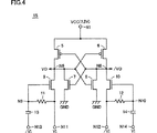
以下、この実施の形態1の種々の変更例について説明する。図4のレベルシフタ15では、N型TFT7,8のソースが接地される。この変更例では、N型TFT7,8の電流を入力ノードN11,N12に流さずに接地電位GNDのラインに流すので、入力信号VI,/VIの駆動力が小さくて済む。
【0048】
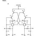
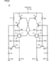
図5のレベルシフタ16が図2のレベルシフタ3と異なる点は、P型TFT17,18が追加されている点である。P型TFT17は、P型TFT5のドレインとノードN5との間に介挿され、そのゲートはノードN9に接続される。P型TFT18は、P型TFT6のドレインとノードN6との間に介挿され、そのゲートはノードN10に接続される。この変更例では、たとえば、入力信号/VIが「L」レベル(0V)から「H」レベル(3V)に立上げられたときに(図3の時刻t1参照)、P型TFT17が導通状態から非導通状態に変化し、電源電位VCCのノードN1から出力ノードN5に流入する電流を抑制するので、出力ノードN5の電位が低下しやすくなる。この結果、P型TFT6が迅速に導通してノードN6の電位が上昇しやすくなる。また、上述のように、P型TFT17,18が非導通になることによって電源電位VCCのノードN1から出力ノードN5,N6に流入する電流が抑制されるので、消費電力が小さくて済む。
【0049】
図6のレベルシフタ20が図2のレベルシフタ3と異なる点は、抵抗素子11,12がそれぞれN型TFT21,22で置換されている点である。N型TFT21は、ノードN9とN11の間に接続され、そのゲートは電源電位VCCを受ける。N型TFT22は、ノードN10とN12の間に接続され、そのゲートは電源電位VCCを受ける。N型TFT21,22の各々は、等価的に抵抗素子の働きをする。図2の抵抗素子11,12に比べて単位寸法当りの抵抗値が高いので、抵抗素子としての占有面積が小さくなる。なお、N型TFT21,22の各々をP型TFTで置換してもよい。ただし、この場合はP型TFTのゲートに負電圧(−7.5V)を与える必要がある。
【0050】
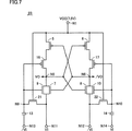
図7のレベルシフタ23が図5のレベルシフタ16と異なる点は、抵抗素子11,12がそれぞれN型TFT21,22で置換されている点である。したがって、この変更例では、図5の変更例と図6の変更例の両方の効果を有する。
【0051】
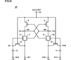
図8のレベルシフタ25は、図5のレベルシフタ16にダイオード素子26,27を追加したものである。ダイオード素子26はノードN11とN9の間に接続され、ダイオード素子27はノードN12とN14の間に接続される。ダイオード素子26は、入力信号VIが「L」レベル(0V)から「H」レベル(3V)に立上げられたとき、ノードN9の「H」レベル(3V)への上昇を速くする(図3参照)。これにより、次に入力信号/VIが「L」レベル(0V)から「H」レベル(3V)に立上げられたときにノードN9の「H」レベル(3V)への立上がりが速くなり、N型TFT9は迅速に導通する。ダイオード素子27は、N型TFT10に対してダイオード素子26と同じ働きをする。したがって、この変更例では、入力信号VI,/VIのレベル変化に対する出力信号VO,/VOのレベル変化が速くなる。
【0052】
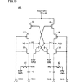
[実施の形態2]
図9は、この発明の実施の形態2によるレベルシフタ30の構成を示す回路図であって、図7と対比される図である。図9を参照して、このレベルシフタ30が図7のレベルシフタ23と異なる点は、抵抗素子31,32およびキャパシタ33,34が追加されている点である。抵抗素子31は電源電位VCCのノードN1とN型TFT21のゲート(ノードN21)との間に介挿され、抵抗素子32はノードN1とN型TFT22のゲート(ノードN22)との間に介挿される。キャパシタ33はノードN11とN21の間に接続され、キャパシタ34はノードN12とN22の間に接続される。
【0053】
図10は、レベルシフタ30の動作を示すタイムチャートである。図10において、初期状態では、入力信号VI,/VIがそれぞれ「H」レベル(3V)および「L」レベル(0V)にされ、出力信号VO,/VOがそれぞれ「H」レベル(7.5V)および「L」レベル(0V)にされている。ノードN21,N22はそれぞれ抵抗素子31,32を介して電源電位VCC(7.5V)を受けているので、N型TFT21,22は導通している。したがって、ノードN9は入力信号VIと同電位の3Vにされ、ノードN10は入力信号/VIと同電位の0Vにされている。これらの電位関係により、P型TFT5,16およびN型TFT8が導通し、他のTFT6,7,9,10,17は非導通になっている。つまり、出力ノードN5はP型TFT5,16を介して電源電位VCC(7.5V)を受け、出力ノードN6はN型TFT8を介して入力信号/VIの電位(0V)を受けている。
【0054】
次に、ある時刻t1において、入力信号VIが「H」レベル(3V)から「L」レベル(0V)に立下げられるとともに入力信号/VIが「L」レベル(0V)から「H」レベル(3V)に立上げられると、入力信号/VIの電位変化がキャパシタ13を介してノードN9に伝達され、ノードN9の電位は3V以上の電位に上昇する。同時に、入力信号VIの電位変化がキャパシタ33を介してノードN29に伝達され、ノードN21の電位は3V程度低下する。ノードN21の電位が低下するとノードN1から抵抗素子31を介してノードN21に電力が流入し、ノードN21が電源電位VCC(7.5V)に戻る。ノードN21が7.5Vよりも低下している期間はN型TFT21の抵抗値は高くなる。
【0055】
また、時刻t1において、入力信号VIが「H」レベル(3V)から「L」レベル(0V)に立下げられると、ノードN9の電荷がN型TFT21を介してノードN11に放電される。したがって、ノードN9の電位は、3Vから上昇してピーク値に達した後、0Vまで徐々に低下する。
【0056】
このとき、N型TFT21の抵抗値は所定時間だけ比較的高くなるので、ノードN1のレベル低下が図7のレベルシフタ23に比べて緩やかになる。これにより、N型TFT9の導通時間が長くなりノードN5の電位低下が容易になる。
【0057】
他方、ノードN10側では、時刻t1において、入力信号VIが「H」レベル(3V)から「L」レベル(0V)に立下げられるとともに入力信号/VIが「L」レベル(0V)から「H」レベル(3V)に立上げられると、入力信号/VIの電位変化がキャパシタ14を介してノードN10に伝達され、ノードN10の電位は0V以下の電位に低下する。同時に、入力信号/VIの電位変化がキャパシタ34を介してノードN22に伝達され、ノードN22の電位は3V程度上昇する。ノードN22の電位が上昇するとノードN22から抵抗素子32を介してノードN21に電流が流出し、ノードN22が電源電位VCC(7.5V)に戻る。ノードN22の電位が7.5Vよりも高い期間はN型TFT22の抵抗値は低くなる。
【0058】
また、時刻t1において、入力信号/VIが「L」レベル(0V)から「H」レベル(3V)に立上げられると、ノードN12からN型TFT22を介してノードN10に電流が流入する。したがって、ノードN10の電位は、0Vから低下してピーク値に達した後、3Vまで徐々に上昇する。
【0059】
このとき、N型TFT22の抵抗値が所定時間だけ比較的低くなるので、ノードN10のレベル上昇が図7のレベルシフタ23に比べて速くなる。これにより、次の時刻t2におけるノードN10の昇圧を容易に行なうことができる。
【0060】
以上より、このレベルシフタ30の動作マージンはレベルシフタ23の動作マージンよりも大きくなる。
【0061】
なお、この実施の形態2では、抵抗素子31,32の一方電極を電源電位VCC(7.5V)のノードN1に接続したが、電源電位VCCとは異なる正の電源電位のノードに接続してもよい。
【0062】
また、抵抗素子31,32の各々をN型TFTまたはP型TFTで構成してもよい。N型TFTのゲートには電源電位VCCよりも高い正電位を与え、P型TFTのゲートには電源電位VCCよりも低い電位を与えるとよい。また、P型TFT16,17を削除してもよい。
【0063】
[実施の形態3]
図11は、この発明の実施の形態3によるレベルシフタ35の構成を示す回路図であって、図9と対比される図である。図11を参照して、このレベルシフタ35が図9のレベルシフタ30と異なる点は、N型TFT21,22がP型TFT36,37で置換されている点である。P型TFT36は、ノードN9とN11の間に接続され、そのゲートはノードN21に接続される。P型TFT37は、ノードN10とN12の間に接続され、そのゲートはノードN22に接続される。
【0064】
また、抵抗素子31は、ノードN21と負の電源電位−VCC(−7.5V)のノードN31との間に接続される。抵抗素子32は、ノードN22と負の電源電位−VCC(−7.5V)のノードN32との間に接続される。キャパシタ33はノードN13とN21の間に接続され、キャパシタ34はノードN14とN22の間に接続される。
【0065】
図12は、レベルシフタ35の動作を示すタイムチャートである。図12において、初期状態では、入力信号VI,/VIがそれぞれ「H」レベル(3V)および「L」レベル(0V)にされ、出力信号VO,/VOがそれぞれ「H」レベル(7.5V)および「L」レベル(0V)にされている。ノードN21,N22はそれぞれ抵抗素子31,32を介して負の電源電位−VCC(−7.5V)を受けているので、P型TFT36,37は導通している。したがって、ノードN9は入力信号VIと同電位の3Vにされ、ノードN10は入力信号/VIと同電位の0Vにされている。これらの電位関係により、P型TFT5,16およびN型TFT8が導通し、他のTFT6,7,9,10,17は非導通になっている。つまり、出力ノードN5はP型TFT5,16を介して電源電位VCC(7.5V)を受け、出力ノードN6はN型TFT8を介して入力信号/VIの電位(0V)を受けている。
【0066】
次に、ある時刻t1において、入力信号VIが「H」レベル(3V)から「L」レベル(0V)に立下げられるとともに入力信号/VIが「L」レベル(0V)から「H」レベル(3V)に立上げられると、入力信号/VIの電位変化がキャパシタ13を介してノードN9に伝達され、ノードN9の電位は3V以上の電位に上昇する。同時に、入力信号/VIの電位変化がキャパシタ33を介してノードN21に伝達され、ノードN21の電位は3V程度上昇する。ノードN21の電位が上昇するとノードN21から抵抗素子31を介してノードN31に電流が流出し、ノードN21は負の電源電位−VCC(−7.5V)に戻る。ノードN21の電位が−7.5Vよりも高い期間はP型TFT36の抵抗値は高くなる。
【0067】
また、時刻t1において、入力信号VIが「H」レベル(3V)から「L」レベル(0V)に立下げられると、ノードN9の電荷がP型TFT36を介してノードN11に放電される。したがって、ノードN9の電位は、3Vから上昇してピーク値に達した後、0Vまで徐々に低下する。
【0068】
このとき、P型TFT36の抵抗値が所定時間だけ比較的高くなるので、ノードN9のレベル低下が図7のレベルシフタ23に比べて緩やかになる。これにより、N型TFT9の導通時間が長くなりノードN5の電位低下が容易になる。
【0069】
他方、ノードN10側では、時刻t1において、入力信号VIが「H」レベル(3V)から「L」レベル(0V)に立下げられるとともに入力信号/VIが「L」レベル(0V)から「H」レベル(3V)に立上げられると、入力信号VIの電位変化がキャパシタ14を介してノードN10に伝達され、ノードN10の電位は0V以下の電位に低下する。同時に入力信号VIの電位変化がキャパシタ34を介してノードN22に伝達され、ノードN22の電位は3V程度低下する。ノードN22の電位が低下するとノードN32から抵抗素子32を介してノードN20に電流が流入し、ノードN22が負の電源電位−VCC(−7.5V)に戻る。ノードN22の電位が−7.5Vよりも低い期間はP型TFT37の抵抗値は低くなる。
【0070】
また、時刻t1において、入力信号/VIが「L」レベル(0V)から「H」レベル(3V)に立上げられると、ノードN12からP型TFT37を介してノードN10に電流が流入する。したがって、ノードN10の電位は、0Vから低下してピーク値に達した後、3Vまで徐々に上昇する。
【0071】
このとき、P型TFT37の抵抗値が所定時間だけ比較的低くなるので、ノードN10のレベル上昇は図7のレベルシフタ23に比べて早くなる。これにより、次の時刻t2におけるノードN10の昇圧を容易に行なうことができる。
【0072】
以上より、このレベルシフタ35の動作マージンはレベルシフタ23の動作マージンよりも大きくなる。
【0073】
なお、抵抗素子31,32の各々をN型TFTまたはP型TFTで構成してもよい。N型TFTのゲートには正の電源電位VCCよりも高い電位を与え、P型TFTのゲートには負の電源電位−VCCよりも低い負電位を与えるとよい。また、P型TFT16,17を削除してもよい。
【0074】
[実施の形態4]
図13は、この発明の実施の形態4によるレベルシフタ40の構成を示す回路図であって、図5と対比される図である。
【0075】
図13において、このレベルシフタ40が図5のレベルシフタ16と異なる点は、N型TFT7,8のソースがともに接地され、抵抗素子11,12およびキャパシタ13,14が抵抗素子41,42およびキャパシタ43,44で置換されている点である。
【0076】
キャパシタ43は入力ノードN11とN型TFT9のソース(ノードN41)との間に接続され、キャパシタ44は入力ノードN12とN型TFT10のソース(ノードN42)との間に接続される。抵抗素子41,42は、それぞれノードN41,N42と接地電位GNDのラインとの間に接続される。入力信号/VIはTFT9,17のゲートに直接与えられ、入力信号VIはTFT10,18のゲートに直接与えられる。
【0077】
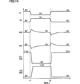
図14は、レベルシフタ40の動作を示すタイムチャートである。図14を参照して、初期状態では、入力信号VI,/VIがそれぞれ「H」レベル(3V)および「L」レベル(0V)にされ、出力信号VO,/VOがそれぞれ「H」レベル(7.5V)および「L」レベル(0V)にされている。ノードN41,N42は、抵抗素子41,42によって接地電位GNDにされている。これらの電位関係により、P型TFT5,17およびN型TFT8,10が導通し、他のTFT6,7,9,18は非導通になっている。つまり、出力ノードN5はP型TFT5,7を介して電源電位VCC(7.5V)を受け、出力ノードN6はN型TFT8を介して接地電位GND(0V)を受けている。
【0078】
次に、ある時刻t1において、入力信号VIが「H」レベル(3V)から「L」レベル(0V)に立下げられるとともに入力信号/VIが「L」レベル(0V)から「H」レベル(3V)に立上げられると、入力信号VIの電位変化がキャパシタ43を介してノードN41に伝達され、ノードN41は接地電位GND(0V)以下の電位に低下する。電位の低下分は、キャパシタ43の容量値とノードN41の寄生容量(図示せず)の容量値との比で決まる。キャパシタ43の容量値を寄生容量の容量値よりも十分大きな値に設定すると、ノードN41の電位は入力信号VIの振幅電圧分だけ低下し、−3Vまで低下する。
【0079】
ノードN41の電位が約−3Vまで低下すると、接地電位GNDのラインから抵抗素子41を介してノードN41に電流が流入する。したがって、ノードN41の電位は、0Vから低下してピーク値に達した後、0Vまで徐々に上昇する。ここで、抵抗素子41の抵抗値を適切に設定することにより、ノードN41の電位を所定時間だけ0V以下の所定電位に保持させることができる。
【0080】
ノードN41が所定電位になると、N型TFT9のゲート−ソース間の電圧が3V〜6Vになり、N型TFT9が導通してノードN5の電位が低下する。ノードN5の電位が低下すると、P型TFT6が導通してノードN6の電位が上昇する。このように、P型TFT5が非導通になるとともにN型TFT7が導通し、出力ノードN5の電位が急速に「L」レベル(0V)に低下する。
【0081】
一方、入力信号/VIの「L」レベル(0V)から「H」レベル(3V)への電位変化がキャパシタ44を介してノードN42に伝達され、ノードN42の電位は0Vから3V近くまで上昇する。しかし、N型TFT10は既に非導通になっているので、回路動作への影響はない。
【0082】
以上の結果、出力信号VOが「H」レベル(7.5V)から「L」レベル(0V)に立下げられるとともに出力信号/VOが「L」レベル(0V)から「H」レベル(7.5V)に立上げられ、3Vから7.5Vへの論理レベルの変換が行なわれたことになる。
【0083】
ノードN41,N42の電位は、それぞれ、抵抗素子41,42によって時間の経過とともにそれぞれ接地電位GNDに近づき、時刻t2ではノードN41,N42の電位はほぼ接地電位GNDになっている。時刻t2において、入力信号VIが「L」レベル(0V)から「H」レベル(3V)に立上げられるとともに入力信号/VIが「H」レベル(3V)から「L」レベル(0V)に立下げられると、上記と逆の電位関係で回路が動作する。
【0084】
この実施の形態4でも、実施の形態1と同じ効果が得られる。
なお図15に示すように、実施の形態2に従って、抵抗素子41,42をそれぞれN型TFT21,22で置換し、N型TFT21,22のゲート(ノードN21,N22)とノードN1との間にそれぞれ抵抗素子31,32を接続し、ノードN11,N12とノードN21,N22との間にそれぞれキャパシタ33,34を接続してもよい。図16に示すように、時刻t1において入力信号VIが「H」レベル(3V)から「L」レベル(0V)に立下げられると、ノードN21の電位が約3V低下し、所定時間だけ電源電位VCC(7.5V)よりも低くなる。ノードN21の電位が7.5Vよりも低くなると、N型TFT21の抵抗値は高くなる。したがって、ノードN41のレベル上昇が図13のレベルシフタ40よりも緩やかになり、出力ノードN5を「L」レベルに引下げやすくなる。また、時刻t1において入力信号/VIが「L」レベル(0V)から「H」レベル(3V)に立上げられると、ノードN22の電位が約3V上昇し、所定時間だけ電源電位VCC(7.5V)よりも高くなる。ノードN21の電位が7.5Vよりも高くなると、N型TFT22の抵抗値が低くなる。したがって、ノードN42のレベル低下が図13のレベルシフタ40よりも早くなり、次の時刻t2におけるノードN42の降圧動作を容易に行なうことができる。
【0085】
今回開示された実施の形態はすべての点で例示であって制限的なものではないと考えられるべきである。本発明の範囲は上記した説明ではなくて特許請求の範囲によって示され、特許請求の範囲と均等の意味および範囲内でのすべての変更が含まれることが意図される。
【図面の簡単な説明】
【図1】 この発明の実施の形態1による携帯電話機の画像表示に関連する部分を示すブロック図である。
【図2】 図1に示したレベルシフタの構成を示す回路図である。
【図3】 図2に示したレベルシフタの動作を示すタイムチャートである。
【図4】 実施の形態1の変更例を示す回路図である。
【図5】 実施の形態1の他の変更例を示す回路図である。
【図6】 実施の形態1のさらに他の変更例を示す回路図である。
【図7】 実施の形態1のさらに他の変更例を示す回路図である。
【図8】 実施の形態1のさらに他の変更例を示す回路図である。
【図9】 この発明の実施の形態2によるレベルシフタの構成を示す回路図である。
【図10】 図9に示したレベルシフタの動作を示すタイムチャートである。
【図11】 この発明の実施の形態3によるレベルシフタの構成を示す回路図である。
【図12】 図11に示したレベルシフタの動作を示すタイムチャートである。
【図13】 この発明の実施の形態4によるレベルシフタの構成を示す回路図である。
【図14】 図13に示したレベルシフタの動作を示すタイムチャートである。
【図15】 実施の形態4の変更例を示す回路図である。
【図16】 図15に示したレベルシフタの動作を示すタイムチャートである。
【図17】 従来の携帯電話機の画像表示に関連する部分を示すブロック図である。
【図18】 図17に示したレベルシフタの構成を示す回路図である。
【図19】 従来の他のレベルシフタの構成を示す回路図である。[0001]
BACKGROUND OF THE INVENTION
The present invention relates to an amplitude conversion circuit, and more particularly to an amplitude conversion circuit for converting the amplitude of a signal.
[0002]
[Prior art]
FIG. 17 is a block diagram showing a configuration of a portion related to image display of a conventional mobile phone.
[0003]
In FIG. 17, this mobile phone includes a
[0004]
The
[0005]
FIG. 18 is a circuit diagram showing a configuration of the
[0006]
Now, the input signals VI and / VI are set to “L” level (0V) and “H” level (3V), respectively, and the output signals VO and / VO are respectively set to “H” level (7.5V) and “L” level. It is assumed that it is set to (0V). At this time, the
[0007]
In this state, the input signal VI rises from the “L” level (0 V) to the “H” level (3 V) and the input signal / VI rises from the “H” level (3 V) to the “L” level (0 V). When lowered, N
[0008]
FIG. 19 shows another conventional level shifter 6.0FIG. Referring to FIG. 19,
[0009]
In
[0010]
Thus, in
[0011]
In a general semiconductor LSI, it is easy to reduce the threshold voltage of a transistor to 3 V or less. However, a low-temperature polysilicon TFT included in a liquid crystal display device has a large threshold voltage variation, and the threshold of the TFT is low. It is difficult to make the
[0012]
[Problems to be solved by the invention]
However, when
[0013]
Therefore, a main object of the present invention is to provide an amplitude conversion circuit which operates normally even when the amplitude voltage of the input signal is lower than the threshold voltage of the input transistor.
[0014]
[Means for solving the problems and effects]
The amplitude conversion circuit according to the present invention converts a first signal whose amplitude is a first voltage into a second signal whose second amplitude is a second voltage higher than the first voltage. . In this amplitude conversion circuit, both of the first electrodes receive the second voltage, and the second electrodes are supplied to the first and second output nodes for outputting the second signal and its complementary signal. First and second transistors of the first conductivity type, each connected and having their input electrodes connected to the second and first output nodes, respectively, and those first electrodes being first and second, respectively. Driven by the first signal and its complementary signal, and in response to the leading edge of the first signal, from the first voltage A third voltage is applied between the input electrode and the second electrode of the third transistor to cause the third transistor to conduct, and the third voltage is applied to the fourth signal in response to the trailing edge of the first signal. Transistor input electrode and second It is provided a drive circuit for turning the fourth transistor is given between the electrodes.
[0015]
thisThe driving circuit includes a first resistance element connected between the input electrode and the second electrode of the third transistor, one electrode receiving a complementary signal of the first signal, and the other electrode being the third transistor. A first capacitor connected to the input electrode of the second transistor, a second resistance element connected between the input electrode and the second electrode of the fourth transistor, one electrode receiving the first signal, and the other And a second capacitor connected to the input electrode of the fourth transistor for providing the first signal and its complementary signal to the second electrode of the third and fourth transistors, respectively.Accordingly, in response to the leading edge or the trailing edge of the first signal, a third voltage higher than the first voltage, which is the amplitude voltage of the first signal, is applied to the input electrode of the third or fourth transistor and the second voltage. So that the first signal operates even when the amplitude voltage of the first signal is lower than the threshold voltage of the third and fourth transistors.The
[0016]
Preferably, the first resistance element includes an input electrode and a second electrode of the third transistor.whileAnd a fifth transistor whose input electrode receives the fourth voltage. The second resistance element includes a sixth transistor that is connected between the input electrode and the second electrode of the fourth transistor, and whose input electrode receives the fourth voltage. In this case, the area occupied by the first and second resistance elements may be small.
[0017]
Also preferably, the fifth and sixth transistors are of the second conductivity type, and the fourth voltage is equal to the second voltage. In this case, the number of voltage sources can be small.
[0018]
Preferably, the first resistance element includes a fifth transistor connected between the input electrode and the second electrode of the third transistor. The second resistance element includes a sixth transistor connected between the input electrode and the second electrode of the fourth transistor. The driving circuit further increases the resistance value of the fifth transistor in a pulse manner in response to the leading edge of the first signal, and increases the resistance value of the sixth transistor in response to the trailing edge of the first signal. A pulse generation circuit for increasing the pulse is included. In this case, the potential drop of the input electrodes of the third and fourth transistors can be moderated.
[0019]
Also preferably, the fifth and sixth transistors are of the second conductivity type. The pulse generation circuit includes a third resistance element connected between a node of a fourth voltage having the same polarity as the second voltage and an input electrode of the fifth transistor, and one of the electrodes generates a first signal. A third capacitor having the other electrode connected to the input electrode of the fifth transistor, and a fourth resistance element connected between the node of the fourth voltage and the input electrode of the sixth transistor; , One electrode receiving a complementary signal of the first signal and the other electrode including a fourth capacitor connected to the input electrode of the sixth transistor. In this case, the input electrode of the fifth or sixth transistor charged to the fourth voltage via the third or fourth resistance element is equivalent to the first voltage via the third or fourth capacitor. Step down.
[0020]
Also preferably, the fourth voltage is equal to the second voltage. In this case, the number of voltage sources can be small.
[0021]
Also preferably, the fifth and sixth transistors are of the first conductivity type. The pulse generation circuit includes a third resistance element connected between a node of a fourth voltage having a polarity opposite to that of the second voltage and an input electrode of the fifth transistor, and one electrode of the first signal Receiving a complementary signal, a fourth capacitor connected between the third capacitor having the other electrode connected to the input electrode of the fifth transistor and the node of the fourth voltage and the input electrode of the sixth transistor; The resistor element includes a fourth capacitor having one electrode receiving the first signal and the other electrode connected to the input electrode of the sixth transistor. In this case, the input electrode of the fifth or sixth transistor charged to the fourth voltage via the third or fourth resistance element is equivalent to the first voltage via the third or fourth capacitor. Boosted.
[0022]
Preferably, the drive circuit is further connected between the first diode element connected between the second electrode and the input electrode of the third transistor, and between the second electrode and the input electrode of the fourth transistor. And a second diode element. In this case, the input electrode of the third or fourth transistor can be quickly charged to the first voltage.
[0023]
AlsoOther amplitude conversion circuit according to the present inventionIsThe first signal whose amplitude is the first voltage is converted into a second signal whose second amplitude is higher than the first voltage. In this amplitude conversion circuit, both of the first electrodes receive the second voltage, and the second electrodes are supplied to the first and second output nodes for outputting the second signal and its complementary signal. First and second transistors of the first conductivity type, each connected and having their input electrodes connected to the second and first output nodes, respectively, and those first electrodes being first and second, respectively. Driven by the first signal and its complementary signal, and in response to the leading edge of the first signal, from the first voltage A third voltage is applied between the input electrode and the second electrode of the third transistor to cause the third transistor to conduct, and the third voltage is applied to the fourth signal in response to the trailing edge of the first signal. Transistor input electrode and second A drive circuit for turning the fourth transistor is given between the electrodes is provided. thisThe driving circuit includes a first resistance element connected between the second electrode of the third transistor and the node of the reference voltage, one electrode receiving the first signal, and the other electrode being the third electrode. A first capacitor connected to the second electrode of the transistor; a second resistance element connected between the second electrode of the fourth transistor and a node of the reference voltage; And a second capacitor whose other electrode is connected to the second electrode of the fourth transistor, the first signal and its complementary signal being respectively received by the fourth and third transistors. To the input electrode.Accordingly, in response to the leading edge or the trailing edge of the first signal, a third voltage higher than the first voltage, which is the amplitude voltage of the first signal, is applied to the input electrode of the third or fourth transistor and the second voltage. So that the first signal operates even when the amplitude voltage of the first signal is lower than the threshold voltage of the third and fourth transistors.The
[0024]
Preferably, the first resistance element includes a fifth transistor connected between the second electrode of the third transistor and the node of the reference voltage. The second resistance element includes a sixth transistor connected between the second electrode of the second transistor and the node of the reference voltage. The driving circuit further increases the resistance value of the fifth transistor in a pulse manner in response to the leading edge of the first signal, and increases the resistance value of the sixth transistor in response to the trailing edge of the first signal. A pulse generation circuit for increasing the pulse is included. In this case, the voltage increase of the input electrodes of the third and fourth transistors can be moderated.
[0025]
Also preferably, the fifth and sixth transistors are of the second conductivity type. The pulse generation circuit includes a third resistance element connected between a node of a fourth voltage having the same polarity as the second voltage and an input electrode of the fifth transistor, and one of the electrodes generates a first signal. A third capacitor having the other electrode connected to the input electrode of the fifth transistor, and a fourth resistance element connected between the node of the fourth voltage and the input electrode of the sixth transistor; , One electrode receiving a complementary signal of the first signal and the other electrode including a fourth capacitor connected to the input electrode of the sixth transistor. In this case, the input electrode of the fifth or sixth transistor charged to the fourth voltage via the third or fourth resistance element is equivalent to the first voltage via the third or fourth capacitor. Step down.
[0026]
Also preferably, the fourth voltage is equal to the second voltage. In this case, the number of voltage sources can be small.
[0027]
Preferably, a latch circuit is further provided for latching the potentials of the first and second output nodes. In this case, the potentials of the first and second output nodes can be held stably.
[0028]
Also preferably, the latch circuit has the first electrodes connected to the first and second output nodes, respectively, the second electrodes respectively receiving the first signal and its complementary signal, and their inputs. The electrodes include fifth and sixth transistors of the second conductivity type connected to the second and first output nodes, respectively. In this case, the latch circuit can be easily configured.
[0029]
Preferably, the latch circuit is connected between the first and second output nodes and the node of the reference voltage, respectively, and the input electrodes thereof are connected to the second and first output nodes, respectively. It includes fifth and sixth transistors of conductive type. In this case, the driving force of the first signal and its complementary signal can be small.
[0030]
Further preferably, the first conductive type having a first conductivity type interposed between the second electrode of the first transistor and the first output node, the input electrode of which is connected to the input electrode of the third transistor. The fifth transistor, the second electrode of the second transistor, and the second output node are interposed between the input electrodes of the fourth transistor and the first conductivity type. And a sixth transistor. In this case, current flowing from the second voltage node to the first and second output nodes can be reduced, and current consumption can be reduced.
[0031]
Preferably, the first to fourth transistors are thin film transistors. The present invention is particularly effective in this case.
[0032]
DETAILED DESCRIPTION OF THE INVENTION
[Embodiment 1]
FIG. 1 is a block diagram showing a configuration of a portion related to image display of a mobile phone according to
[0033]
In FIG. 1, the cellular phone includes a
[0034]
The
[0035]
FIG. 2 is a circuit diagram showing the configuration of the
[0036]
N-
[0037]
FIG. 3 is a time chart showing the operation of the
[0038]
Next, at a certain time t1, the input signal VI falls from the “H” level (3V) to the “L” level (0V) and the input signal / VI changes from the “L” level (0V) to the “H” level ( 3V), the potential change of the input signal / VI is transmitted to the node N9 via the
[0039]
On the other hand, input signal VI falls from “H” level (3 V) to “L” level (0 V) simultaneously with / VI, so that the charge at node N9 is discharged to node N11 via
[0040]
On the other hand, the potential change of the input signal VI from the “H” level (3V) to the “L” level (0V) is transmitted to the node N10 via the
[0041]
As a result, the output signal VO is lowered from the “H” level (7.5 V) to the “L” level (0 V) and the output signal / VO is changed from the “L” level (0 V) to the “H” level (7. 5V), and a logic level conversion from 3V to 7.5V has been performed.
[0042]
The potentials of the nodes N9 and N10 are shifted to the levels of the input signals VI and / VI with the passage of time by the
[0043]
In the first embodiment, in response to the falling edge of the input signal VI, a voltage (about 6V) higher than the amplitude voltage (3V) of the input signal VI is generated and applied between the gate and source of the N-
[0044]
Although the power supply current flows transiently during the operation, after the levels of the output nodes N5 and N6 are determined, the
[0045]
Although the
[0046]
In the first embodiment, a TFT which is an insulated gate field effect transistor is used. Needless to say, other types of field effect transistors may be used.
[0047]
Hereinafter, various modifications of the first embodiment will be described. In the
[0048]
The
[0049]
The
[0050]
The
[0051]
The
[0052]
[Embodiment 2]
FIG. 9 is a circuit diagram showing the configuration of the
[0053]
FIG. 10 is a time chart showing the operation of the
[0054]
Next, at a certain time t1, the input signal VI falls from the “H” level (3V) to the “L” level (0V) and the input signal / VI changes from the “L” level (0V) to the “H” level ( 3V), the potential change of the input signal / VI is transmitted to the node N9 via the
[0055]
At time t1, when the input signal VI falls from the “H” level (3V) to the “L” level (0V), the charge at the node N9 is discharged to the node N11 via the N-
[0056]
At this time, since the resistance value of the N-
[0057]
On the other hand, on the node N10 side, at time t1, the input signal VI falls from the “H” level (3V) to the “L” level (0V) and the input signal / VI changes from the “L” level (0V) to “H”. When the voltage is raised to the level (3V), the potential change of input signal / VI is transmitted to node N10 via
[0058]
Further, when the input signal / VI rises from the “L” level (0 V) to the “H” level (3 V) at time t1, a current flows from the node N12 to the node N10 via the N-
[0059]
At this time, since the resistance value of the N-
[0060]
As described above, the operation margin of the
[0061]
In the second embodiment, one electrode of
[0062]
Each of the
[0063]
[Embodiment 3]
FIG. 11 is a circuit diagram showing a configuration of the
[0064]
[0065]
FIG. 12 is a time chart showing the operation of the
[0066]
Next, at a certain time t1, the input signal VI falls from the “H” level (3V) to the “L” level (0V), and the input signal / VI becomes “L"From level (0V) to"HWhen raised to the level (3V), the potential change of input signal / VI is transmitted to node N9 through
[0067]
At time t1, when the input signal VI falls from the “H” level (3V) to the “L” level (0V), the charge at the node N9 is discharged to the node N11 via the P-type TFT. Therefore, the potential of the node N9 rises from 3V and reaches a peak value, and then gradually decreases to 0V.
[0068]
At this time, since the resistance value of the P-
[0069]
On the other hand, on the node N10 side, at time t1, the input signal VI falls from the “H” level (3V) to the “L” level (0V) and the input signal / VI changes from the “L” level (0V) to “H”. When raised to the level (3V), the potential change of the input signal VI is transmitted to the node N10 via the
[0070]
Further, when the input signal / VI rises from the “L” level (0 V) to the “H” level (3 V) at time t1, a current flows from the node N12 to the node N10 via the P-
[0071]
At this time, since the resistance value of the P-
[0072]
As described above, the operation margin of the
[0073]
Each of the
[0074]
[Embodiment 4]
FIG. 13 is a circuit diagram showing a configuration of a
[0075]
13, the
[0076]
The
[0077]
FIG. 14 is a time chart showing the operation of the
[0078]
Next, at a certain time t1, the input signal VI falls from the “H” level (3V) to the “L” level (0V) and the input signal / VI changes from the “L” level (0V) to the “H” level ( 3V), the potential change of the input signal VI is transmitted to the node N41 via the
[0079]
When the potential of the node N41 decreases to about −3V, a current flows into the node N41 from the ground potential GND line via the
[0080]
When the node N41 becomes a predetermined potential, the voltage between the gate and the source of the N-
[0081]
On the other hand, the potential change of the input signal / VI from the “L” level (0V) to the “H” level (3V) is transmitted to the node N42 via the
[0082]
As a result, the output signal VO is lowered from the “H” level (7.5 V) to the “L” level (0 V) and the output signal / VO is changed from the “L” level (0 V) to the “H” level (7. 5V), and a logic level conversion from 3V to 7.5V has been performed.
[0083]
The potentials of the nodes N41 and N42 approach the ground potential GND with the passage of time by the
[0084]
In the fourth embodiment, the same effect as in the first embodiment can be obtained.
As shown in FIG. 15, according to the second embodiment,
[0085]
The embodiment disclosed this time should be considered as illustrative in all points and not restrictive. The scope of the present invention is defined by the terms of the claims, rather than the description above, and is intended to include any modifications within the scope and meaning equivalent to the terms of the claims.
[Brief description of the drawings]
FIG. 1 is a block diagram showing portions related to image display of a mobile phone according to
FIG. 2 is a circuit diagram showing a configuration of a level shifter shown in FIG.
FIG. 3 is a time chart showing the operation of the level shifter shown in FIG. 2;
FIG. 4 is a circuit diagram showing a modification of the first embodiment.
FIG. 5 is a circuit diagram showing another modification of the first embodiment.
FIG. 6 is a circuit diagram showing still another modification of the first embodiment.
FIG. 7 is a circuit diagram showing still another modification of the first embodiment.
FIG. 8 is a circuit diagram showing still another modified example of the first embodiment.
FIG. 9 is a circuit diagram showing a configuration of a level shifter according to a second embodiment of the present invention.
10 is a time chart showing the operation of the level shifter shown in FIG. 9;
FIG. 11 is a circuit diagram showing a configuration of a level shifter according to a third embodiment of the present invention.
12 is a time chart showing the operation of the level shifter shown in FIG. 11. FIG.
FIG. 13 is a circuit diagram showing a structure of a level shifter according to
14 is a time chart showing the operation of the level shifter shown in FIG.
FIG. 15 is a circuit diagram showing a modification of the fourth embodiment.
16 is a time chart showing the operation of the level shifter shown in FIG.
FIG. 17 is a block diagram showing portions related to image display of a conventional mobile phone.
FIG. 18 is a circuit diagram showing a configuration of the level shifter shown in FIG. 17;
FIG. 19 is a circuit diagram showing a configuration of another conventional level shifter.
Claims (17)
それらの第1の電極がともに前記第2の電圧を受け、それらの第2の電極が前記第2の信号およびその相補信号を出力するための第1および第2の出力ノードにそれぞれ接続され、それらの入力電極がそれぞれ前記第2および第1の出力ノードに接続された第1の導電形式の第1および第2のトランジスタ、
それらの第1の電極がそれぞれ前記第1および第2の出力ノードに接続された第2の導電形式の第3および第4のトランジスタ、および
前記第1の信号およびその相補信号によって駆動され、前記第1の信号の前縁に応答して前記第1の電圧よりも高い第3の電圧を前記第3のトランジスタの入力電極および第2の電極間に与えて前記第3のトランジスタを導通させ、前記第1の信号の後縁に応答して前記第3の電圧を前記第4のトランジスタの入力電極および第2の電極間に与えて前記第4のトランジスタを導通させる駆動回路を備え、
前記駆動回路は、
前記第3のトランジスタの入力電極および第2の電極間に接続された第1の抵抗素子、
その一方電極が前記第1の信号の相補信号を受け、その他方電極が前記第3のトランジスタの入力電極に接続された第1のキャパシタ、
前記第4のトランジスタの入力電極および第2の電極間に接続された第2の抵抗素子、および
その一方電極が前記第1の信号を受け、その他方電極が前記第4のトランジスタの入力電極に接続された第2のキャパシタを含み、
前記第1の信号およびその相補信号をそれぞれ前記第3および第4のトランジスタの第2の電極に与える、振幅変換回路。An amplitude conversion circuit that converts a first signal whose amplitude is a first voltage into a second signal whose amplitude is a second voltage higher than the first voltage,
A first electrode thereof are both subjected to the second voltage, respectively connected to the first and second output nodes for their second electrodes to output said second signal and its complementary signal, First and second transistors of a first conductivity type with their input electrodes connected to the second and first output nodes, respectively;
The first electrodes are driven by the third and fourth transistors of the second conductivity type connected to the first and second output nodes, respectively, and the first signal and its complementary signal; Providing a third voltage higher than the first voltage in response to the leading edge of the first signal between the input electrode and the second electrode of the third transistor to cause the third transistor to conduct; A drive circuit for applying the third voltage between the input electrode and the second electrode of the fourth transistor in response to the trailing edge of the first signal to make the fourth transistor conductive ;
The drive circuit is
A first resistance element connected between an input electrode and a second electrode of the third transistor;
A first capacitor having one electrode receiving a complementary signal of the first signal and the other electrode connected to an input electrode of the third transistor;
A second resistance element connected between an input electrode and a second electrode of the fourth transistor; and
A second capacitor having one electrode receiving the first signal and the other electrode connected to the input electrode of the fourth transistor;
Ru given the first signal and the complementary signal to the respective second electrodes of said third and fourth transistors, the amplitude conversion circuit.
前記第2の抵抗素子は、前記第4のトランジスタの入力電極および第2の電極間に接続され、その入力電極が前記第4の電圧を受ける第6のトランジスタを含む、請求項1に記載の振幅変換回路。The first resistance element includes a fifth transistor connected between the input electrode and the second electrode of the third transistor, the input electrode receiving a fourth voltage;
The second resistor element, the fourth is connected between the input electrode and the second electrode of the transistor, a sixth transistor having an input electrode receiving said fourth voltage, according to claim 1 Amplitude conversion circuit.
前記第4の電圧は前記第2の電圧に等しい、請求項2に記載の振幅変換回路。The fifth and sixth transistors are of a second conductivity type;
The amplitude conversion circuit according to claim 2 , wherein the fourth voltage is equal to the second voltage.
前記第2の抵抗素子は、前記第4のトランジスタの入力電極および第2の電極間に接続された第6のトランジスタを含み、
前記駆動回路は、さらに、前記第1の信号の前縁に応答して前記第5のトランジスタの抵抗値をパルス的に高くし、前記第1の信号の後縁に応答して前記第6のトランジスタの抵抗値をパルス的に高くするためのパルス発生回路を含む、請求項1に記載の振幅変換回路。The first resistance element includes a fifth transistor connected between an input electrode and a second electrode of the third transistor,
The second resistance element includes a sixth transistor connected between an input electrode and a second electrode of the fourth transistor,
The drive circuit further increases the resistance value of the fifth transistor in a pulse manner in response to the leading edge of the first signal, and the sixth circuit in response to the trailing edge of the first signal. 2. The amplitude conversion circuit according to claim 1 , further comprising a pulse generation circuit for increasing the resistance value of the transistor in a pulse manner.
前記パルス発生回路は、
前記第2の電圧と同極性の第4の電圧のノードと前記第5のトランジスタの入力電極との間に接続された第3の抵抗素子、
その一方電極が前記第1の信号を受け、その他方電極が前記第5のトランジスタの入力電極に接続された第3のキャパシタ、
前記第4の電圧のノードと前記第6のトランジスタの入力電極との間に接続された第4の抵抗素子、および
その一方電極が前記第1の信号の相補信号を受け、その他方電極が前記第6のトランジスタの入力電極に接続された第4のキャパシタを含む、請求項4に記載の振幅変換回路。The fifth and sixth transistors are of a second conductivity type;
The pulse generation circuit includes:
A third resistance element connected between a node of a fourth voltage having the same polarity as the second voltage and an input electrode of the fifth transistor;
A third capacitor having one electrode receiving the first signal and the other electrode connected to the input electrode of the fifth transistor;
A fourth resistance element connected between the node of the fourth voltage and an input electrode of the sixth transistor; and one electrode receives a complementary signal of the first signal, and the other electrode is The amplitude conversion circuit according to claim 4 , further comprising a fourth capacitor connected to the input electrode of the sixth transistor.
前記パルス発生回路は、
前記第2の電圧と逆極性の第4の電圧のノードと前記第5のトランジスタの入力電極との間に接続された第3の抵抗素子、
その一方電極が前記第1の信号の相補信号を受け、その他方電極が前記第5のトランジスタの入力電極に接続された第3のキャパシタ、
前記第4の電圧のノードと前記第6のトランジスタの入力電極との間に接続された第4の抵抗素子、および
その一方電極が前記第1の信号を受け、その他方電極が前記第6のトランジスタの入力電極に接続された第4のキャパシタを含む、請求項4に記載の振幅変換回路。The fifth and sixth transistors are of a first conductivity type;
The pulse generation circuit includes:
A third resistance element connected between a node of a fourth voltage having a polarity opposite to that of the second voltage and an input electrode of the fifth transistor;
A third capacitor having one electrode receiving a complementary signal of the first signal and the other electrode connected to the input electrode of the fifth transistor;
A fourth resistance element connected between the node of the fourth voltage and an input electrode of the sixth transistor; and one electrode receives the first signal, and the other electrode is the sixth The amplitude conversion circuit according to claim 4 , further comprising a fourth capacitor connected to the input electrode of the transistor.
さらに、前記第3のトランジスタの第2の電極および入力電極間に接続された第1のダイオード素子、および
前記第4のトランジスタの第2の電極および入力電極間に接続された第2のダイオード素子を含む、請求項1に記載の振幅変換回路。The drive circuit is
Furthermore, a first diode element connected between the second electrode and the input electrode of the third transistor, and a second diode element connected between the second electrode and the input electrode of the fourth transistor The amplitude conversion circuit according to claim 1 , comprising:
それらの第1の電極がともに前記第2の電圧を受け、それらの第2の電極が前記第2の信号およびその相補信号を出力するための第1および第2の出力ノードにそれぞれ接続され、それらの入力電極がそれぞれ前記第2および第1の出力ノードに接続された第1の導電形式の第1および第2のトランジスタ、
それらの第1の電極がそれぞれ前記第1および第2の出力ノードに接続された第2の導電形式の第3および第4のトランジスタ、および
前記第1の信号およびその相補信号によって駆動され、前記第1の信号の前縁に応答して前記第1の電圧よりも高い第3の電圧を前記第3のトランジスタの入力電極および第2の電極間に与えて前記第3のトランジスタを導通させ、前記第1の信号の後縁に応答して前記第3の電圧を前記第4のトランジスタの入力電極および第2の電極間に与えて前記第4のトランジスタを導通させる駆動回路を備え、
前記駆動回路は、
前記第3のトランジスタの第2の電極と基準電圧のノードとの間に接続された第1の抵抗素子、
その一方電極が前記第1の信号を受け、その他方電極が前記第3のトランジスタの第2の電極に接続された第1のキャパシタ、
前記第4のトランジスタの第2の電極と前記基準電圧のノードとの間に接続された第2の抵抗素子、および
その一方電極が前記第1の信号の相補信号を受け、その他方電極が前記第4のトランジスタの第2の電極に接続された第2のキャパシタを含み、
前記第1の信号およびその相補信号をそれぞれ前記第4および第3のトランジスタの入力電極に与える、振幅変換回路。 An amplitude conversion circuit that converts a first signal whose amplitude is a first voltage into a second signal whose amplitude is a second voltage higher than the first voltage,
Both of the first electrodes receive the second voltage, and the second electrodes are respectively connected to first and second output nodes for outputting the second signal and its complementary signal; First and second transistors of a first conductivity type with their input electrodes connected to the second and first output nodes, respectively;
Third and fourth transistors of a second conductivity type with their first electrodes respectively connected to the first and second output nodes; and
Driven by the first signal and its complementary signal and in response to a leading edge of the first signal, a third voltage higher than the first voltage is applied to an input electrode of the third transistor and a second voltage Providing the third transistor in conduction between the electrodes, and applying the third voltage between the input electrode and the second electrode of the fourth transistor in response to the trailing edge of the first signal, A drive circuit for conducting the fourth transistor;
The drive circuit is
A first resistance element connected between a second electrode of the third transistor and a node of a reference voltage;
A first capacitor having one electrode receiving the first signal and the other electrode connected to a second electrode of the third transistor;
A second resistance element connected between the second electrode of the fourth transistor and the node of the reference voltage; and one electrode receives a complementary signal of the first signal, and the other electrode is the includes a second Capacity data connected to the second electrode of the fourth transistor,
The first signal and the providing complementary signal to the input electrodes of the fourth and third transistors, the amplitude conversion circuit.
前記第2の抵抗素子は、前記第4のトランジスタの第2の電極と前記基準電圧のノードとの間に接続された第6のトランジスタを含み、
前記駆動回路は、さらに、前記第1の信号の前縁に応答して前記第5のトランジスタの抵抗値をパルス的に高くし、前記第1の信号の後縁に応答して前記第6のトランジスタの抵抗値をパルス的に高くするためのパルス発生回路を含む、請求項9に記載の振幅変換回路。The first resistance element includes a fifth transistor connected between a second electrode of the third transistor and a node of the reference voltage,
The second resistance element includes a sixth transistor connected between a second electrode of the fourth transistor and a node of the reference voltage,
The drive circuit further increases the resistance value of the fifth transistor in a pulse manner in response to the leading edge of the first signal, and the sixth circuit in response to the trailing edge of the first signal. 10. The amplitude conversion circuit according to claim 9 , further comprising a pulse generation circuit for increasing the resistance value of the transistor in a pulse manner.
前記パルス発生回路は、
前記第2の電圧と同極性の第4の電圧のノードと前記第5のトランジスタの入力電極との間に接続された第3の抵抗素子、
その一方電極が前記第1の信号を受け、その他方電極が前記第5のトランジスタの入力電極に接続された第3のキャパシタ、
前記第4の電圧のノードと前記第6のトランジスタの入力電極との間に接続された第4の抵抗素子、および
その一方電極が前記第1の信号の相補信号を受け、その他方電極が前記第6のトランジスタの入力電極に接続された第4のキャパシタを含む、請求項10に記載の振幅変換回路。The fifth and sixth transistors are of a second conductivity type;
The pulse generation circuit includes:
A third resistance element connected between a node of a fourth voltage having the same polarity as the second voltage and an input electrode of the fifth transistor;
A third capacitor having one electrode receiving the first signal and the other electrode connected to the input electrode of the fifth transistor;
A fourth resistance element connected between the node of the fourth voltage and an input electrode of the sixth transistor; and one electrode receives a complementary signal of the first signal, and the other electrode is a fourth Capacity data connected to the input electrode of the sixth transistor, the amplitude conversion circuit of claim 1 0.
前記第2のトランジスタの第2の電極と前記第2の出力ノードとの間に介挿され、その入力電極が前記第4のトランジスタの入力電極に接続された第1の導電形式の第6のトランジスタを備える、請求項1または請求項9に記載の振幅変換回路。Furthermore, the first conductivity type second electrode is inserted between the second electrode of the first transistor and the first output node, and the input electrode of the first transistor is connected to the input electrode of the third transistor. 5, and a first conductive element that is interposed between the second electrode of the second transistor and the second output node, and whose input electrode is connected to the input electrode of the fourth transistor. The amplitude conversion circuit according to claim 1 or 9 , comprising a sixth transistor of the type.
Applications Claiming Priority (1)
| Application Number | Priority Date | Filing Date | Title |
|---|---|---|---|
| PCT/JP2002/001760 WO2003073617A1 (en) | 2002-02-26 | 2002-02-26 | Amplitude converting circuit |
Publications (2)
| Publication Number | Publication Date |
|---|---|
| JPWO2003073617A1 JPWO2003073617A1 (en) | 2005-06-23 |
| JP3927953B2 true JP3927953B2 (en) | 2007-06-13 |
Family
ID=27764175
Family Applications (1)
| Application Number | Title | Priority Date | Filing Date |
|---|---|---|---|
| JP2003572178A Expired - Fee Related JP3927953B2 (en) | 2002-02-26 | 2002-02-26 | Amplitude conversion circuit |
Country Status (6)
| Country | Link |
|---|---|
| US (1) | US6861889B2 (en) |
| JP (1) | JP3927953B2 (en) |
| KR (1) | KR100528858B1 (en) |
| CN (1) | CN1258878C (en) |
| TW (1) | TW546623B (en) |
| WO (1) | WO2003073617A1 (en) |
Families Citing this family (14)
| Publication number | Priority date | Publication date | Assignee | Title |
|---|---|---|---|---|
| TWI297476B (en) * | 2004-03-10 | 2008-06-01 | Au Optronics Corp | Voltage level shifter and sequential pulse generator |
| US7200053B2 (en) * | 2004-09-01 | 2007-04-03 | Micron Technology, Inc. | Level shifter for low voltage operation |
| KR100590034B1 (en) * | 2004-10-08 | 2006-06-14 | 삼성에스디아이 주식회사 | Level shifter and display device using the same |
| JP5215534B2 (en) * | 2006-05-19 | 2013-06-19 | 株式会社ジャパンディスプレイイースト | Image display device |
| KR20070111774A (en) * | 2006-05-19 | 2007-11-22 | 삼성전자주식회사 | Level shifter |
| KR20090116088A (en) * | 2008-05-06 | 2009-11-11 | 삼성전자주식회사 | A capacitor-less one transistor semiconductor memory device having improved data retention abilities and operation characteristics |
| US7969808B2 (en) * | 2007-07-20 | 2011-06-28 | Samsung Electronics Co., Ltd. | Memory cell structures, memory arrays, memory devices, memory controllers, and memory systems, and methods of manufacturing and operating the same |
| WO2009022275A1 (en) * | 2007-08-13 | 2009-02-19 | Nxp B.V. | Level shifter circuit |
| KR20100070158A (en) * | 2008-12-17 | 2010-06-25 | 삼성전자주식회사 | Semiconductor memory device comprising capacitor-less dynamic memory cells, and method of operating the same |
| KR101442177B1 (en) * | 2008-12-18 | 2014-09-18 | 삼성전자주식회사 | Methods of fabricating a semiconductor device having a capacitor-less one transistor memory cell |
| KR20130096797A (en) * | 2012-02-23 | 2013-09-02 | 에스케이하이닉스 주식회사 | Voltage level converting circuit |
| US8723578B1 (en) | 2012-12-14 | 2014-05-13 | Palo Alto Research Center Incorporated | Pulse generator circuit |
| US10097183B2 (en) * | 2016-03-30 | 2018-10-09 | Texas Instruments Incorporated | Level shifter and method of calibration |
| US10855281B2 (en) * | 2018-10-04 | 2020-12-01 | Raytheon Company | Wide supply range digital level shifter cell |
Family Cites Families (11)
| Publication number | Priority date | Publication date | Assignee | Title |
|---|---|---|---|---|
| US3801831A (en) | 1972-10-13 | 1974-04-02 | Motorola Inc | Voltage level shifting circuit |
| JPS5759690B2 (en) | 1974-05-27 | 1982-12-16 | Tokyo Shibaura Electric Co | |
| JP3017133B2 (en) * | 1997-06-26 | 2000-03-06 | 日本電気アイシーマイコンシステム株式会社 | Level shifter circuit |
| JP3697873B2 (en) | 1997-12-05 | 2005-09-21 | セイコーエプソン株式会社 | Level shift circuit, signal driver and display device using the same, and semiconductor device |
| JP3481121B2 (en) * | 1998-03-20 | 2003-12-22 | 松下電器産業株式会社 | Level shift circuit |
| IT1304060B1 (en) * | 1998-12-29 | 2001-03-07 | St Microelectronics Srl | LEVEL VARIATOR FOR MULTIPLE POWER VOLTAGE CIRCUIT |
| JP2001085989A (en) * | 1999-09-16 | 2001-03-30 | Matsushita Electric Ind Co Ltd | Signal level conversion circuit and active matrix liquid crystal display device provided with the signal level conversion circuit |
| WO2001056159A1 (en) * | 2000-01-27 | 2001-08-02 | Hitachi, Ltd. | Semiconductor device |
| US6359593B1 (en) * | 2000-08-15 | 2002-03-19 | Receptec Llc | Non-radiating single slotline coupler |
| US20030169224A1 (en) * | 2002-03-11 | 2003-09-11 | Mitsubishi Denki Kabushiki Kaisha | Amplitude conversion circuit for converting signal amplitude and semiconductor device using the amplitude conversion circuit |
| US6980194B2 (en) * | 2002-03-11 | 2005-12-27 | Mitsubishi Denki Kabushiki Kaisha | Amplitude conversion circuit for converting signal amplitude |
-
2002
- 2002-02-26 CN CNB028038436A patent/CN1258878C/en not_active Expired - Fee Related
- 2002-02-26 KR KR10-2003-7013530A patent/KR100528858B1/en not_active IP Right Cessation
- 2002-02-26 US US10/450,268 patent/US6861889B2/en not_active Expired - Fee Related
- 2002-02-26 WO PCT/JP2002/001760 patent/WO2003073617A1/en active Application Filing
- 2002-02-26 JP JP2003572178A patent/JP3927953B2/en not_active Expired - Fee Related
- 2002-03-12 TW TW091104558A patent/TW546623B/en not_active IP Right Cessation
Also Published As
| Publication number | Publication date |
|---|---|
| TW546623B (en) | 2003-08-11 |
| KR100528858B1 (en) | 2005-11-16 |
| US20040041614A1 (en) | 2004-03-04 |
| KR20040000430A (en) | 2004-01-03 |
| WO2003073617A1 (en) | 2003-09-04 |
| CN1258878C (en) | 2006-06-07 |
| US6861889B2 (en) | 2005-03-01 |
| JPWO2003073617A1 (en) | 2005-06-23 |
| CN1488193A (en) | 2004-04-07 |
Similar Documents
| Publication | Publication Date | Title |
|---|---|---|
| JP3037031B2 (en) | Power-on signal generation circuit | |
| US7554379B2 (en) | High-speed, low-power level shifter for mixed signal-level environments | |
| JP3927953B2 (en) | Amplitude conversion circuit | |
| KR100419816B1 (en) | Signal potential conversion circuit | |
| TW200304276A (en) | Drive circuit | |
| US8269547B2 (en) | Bootstrap circuit | |
| WO2004025817A1 (en) | Voltage detecting circuit and internal voltage generating circuit comprising it | |
| US6980194B2 (en) | Amplitude conversion circuit for converting signal amplitude | |
| JP4087229B2 (en) | Amplitude conversion circuit and semiconductor device using the same | |
| CN109427371B (en) | Power switch, memory device and method for providing power switch voltage output | |
| US9768685B2 (en) | Bootstrap circuit | |
| US20030169224A1 (en) | Amplitude conversion circuit for converting signal amplitude and semiconductor device using the amplitude conversion circuit | |
| US11621550B2 (en) | Overcurrent protection circuit, overcurrent protection method, clock signal generation circuit and display device | |
| JP2001077681A (en) | Power on reset signal preparing circuit | |
| JPS6143896B2 (en) | ||
| JPH0677804A (en) | Output circuit | |
| JP4371645B2 (en) | Semiconductor device | |
| JPH07231252A (en) | Level shift circuit | |
| JPS6217896B2 (en) | ||
| JP3714260B2 (en) | Semiconductor integrated circuit | |
| JPH09307420A (en) | Output butter | |
| JPH0799772A (en) | Booster circuit and electric-potential control booster circuit | |
| JPH0737385A (en) | Voltage drop circuit for internal power source | |
| JPH0918331A (en) | Logic circuit | |
| JP2004194154A (en) | Amplitude conversion circuit |
Legal Events
| Date | Code | Title | Description |
|---|---|---|---|
| A521 | Written amendment |
Free format text: JAPANESE INTERMEDIATE CODE: A523 Effective date: 20051107 |
|
| A131 | Notification of reasons for refusal |
Free format text: JAPANESE INTERMEDIATE CODE: A131 Effective date: 20061219 |
|
| A521 | Written amendment |
Free format text: JAPANESE INTERMEDIATE CODE: A523 Effective date: 20070201 |
|
| TRDD | Decision of grant or rejection written | ||
| A01 | Written decision to grant a patent or to grant a registration (utility model) |
Free format text: JAPANESE INTERMEDIATE CODE: A01 Effective date: 20070227 |
|
| A61 | First payment of annual fees (during grant procedure) |
Free format text: JAPANESE INTERMEDIATE CODE: A61 Effective date: 20070305 |
|
| R150 | Certificate of patent or registration of utility model |
Free format text: JAPANESE INTERMEDIATE CODE: R150 |
|
| LAPS | Cancellation because of no payment of annual fees |