JP3918942B2 - Antireflection film forming composition for lithography - Google Patents
Antireflection film forming composition for lithography Download PDFInfo
- Publication number
- JP3918942B2 JP3918942B2 JP2003536822A JP2003536822A JP3918942B2 JP 3918942 B2 JP3918942 B2 JP 3918942B2 JP 2003536822 A JP2003536822 A JP 2003536822A JP 2003536822 A JP2003536822 A JP 2003536822A JP 3918942 B2 JP3918942 B2 JP 3918942B2
- Authority
- JP
- Japan
- Prior art keywords
- polymer
- antireflection film
- average molecular
- molecular weight
- formula
- Prior art date
- Legal status (The legal status is an assumption and is not a legal conclusion. Google has not performed a legal analysis and makes no representation as to the accuracy of the status listed.)
- Expired - Fee Related
Links
- WSIJRQXMWUTEBQ-UHFFFAOYSA-N CC(C)(C(C)(C)N)C(C)(C)I Chemical compound CC(C)(C(C)(C)N)C(C)(C)I WSIJRQXMWUTEBQ-UHFFFAOYSA-N 0.000 description 1
Images
Classifications
-
- G—PHYSICS
- G03—PHOTOGRAPHY; CINEMATOGRAPHY; ANALOGOUS TECHNIQUES USING WAVES OTHER THAN OPTICAL WAVES; ELECTROGRAPHY; HOLOGRAPHY
- G03F—PHOTOMECHANICAL PRODUCTION OF TEXTURED OR PATTERNED SURFACES, e.g. FOR PRINTING, FOR PROCESSING OF SEMICONDUCTOR DEVICES; MATERIALS THEREFOR; ORIGINALS THEREFOR; APPARATUS SPECIALLY ADAPTED THEREFOR
- G03F7/00—Photomechanical, e.g. photolithographic, production of textured or patterned surfaces, e.g. printing surfaces; Materials therefor, e.g. comprising photoresists; Apparatus specially adapted therefor
- G03F7/004—Photosensitive materials
- G03F7/09—Photosensitive materials characterised by structural details, e.g. supports, auxiliary layers
- G03F7/11—Photosensitive materials characterised by structural details, e.g. supports, auxiliary layers having cover layers or intermediate layers, e.g. subbing layers
-
- C—CHEMISTRY; METALLURGY
- C08—ORGANIC MACROMOLECULAR COMPOUNDS; THEIR PREPARATION OR CHEMICAL WORKING-UP; COMPOSITIONS BASED THEREON
- C08L—COMPOSITIONS OF MACROMOLECULAR COMPOUNDS
- C08L63/00—Compositions of epoxy resins; Compositions of derivatives of epoxy resins
-
- C—CHEMISTRY; METALLURGY
- C08—ORGANIC MACROMOLECULAR COMPOUNDS; THEIR PREPARATION OR CHEMICAL WORKING-UP; COMPOSITIONS BASED THEREON
- C08G—MACROMOLECULAR COMPOUNDS OBTAINED OTHERWISE THAN BY REACTIONS ONLY INVOLVING UNSATURATED CARBON-TO-CARBON BONDS
- C08G59/00—Polycondensates containing more than one epoxy group per molecule; Macromolecules obtained by polymerising compounds containing more than one epoxy group per molecule using curing agents or catalysts which react with the epoxy groups
- C08G59/14—Polycondensates modified by chemical after-treatment
- C08G59/1433—Polycondensates modified by chemical after-treatment with organic low-molecular-weight compounds
- C08G59/1438—Polycondensates modified by chemical after-treatment with organic low-molecular-weight compounds containing oxygen
- C08G59/1455—Monocarboxylic acids, anhydrides, halides, or low-molecular-weight esters thereof
-
- C—CHEMISTRY; METALLURGY
- C08—ORGANIC MACROMOLECULAR COMPOUNDS; THEIR PREPARATION OR CHEMICAL WORKING-UP; COMPOSITIONS BASED THEREON
- C08G—MACROMOLECULAR COMPOUNDS OBTAINED OTHERWISE THAN BY REACTIONS ONLY INVOLVING UNSATURATED CARBON-TO-CARBON BONDS
- C08G59/00—Polycondensates containing more than one epoxy group per molecule; Macromolecules obtained by polymerising compounds containing more than one epoxy group per molecule using curing agents or catalysts which react with the epoxy groups
- C08G59/18—Macromolecules obtained by polymerising compounds containing more than one epoxy group per molecule using curing agents or catalysts which react with the epoxy groups ; e.g. general methods of curing
- C08G59/20—Macromolecules obtained by polymerising compounds containing more than one epoxy group per molecule using curing agents or catalysts which react with the epoxy groups ; e.g. general methods of curing characterised by the epoxy compounds used
- C08G59/32—Epoxy compounds containing three or more epoxy groups
- C08G59/3254—Epoxy compounds containing three or more epoxy groups containing atoms other than carbon, hydrogen, oxygen or nitrogen
-
- C—CHEMISTRY; METALLURGY
- C08—ORGANIC MACROMOLECULAR COMPOUNDS; THEIR PREPARATION OR CHEMICAL WORKING-UP; COMPOSITIONS BASED THEREON
- C08L—COMPOSITIONS OF MACROMOLECULAR COMPOUNDS
- C08L71/00—Compositions of polyethers obtained by reactions forming an ether link in the main chain; Compositions of derivatives of such polymers
-
- C—CHEMISTRY; METALLURGY
- C09—DYES; PAINTS; POLISHES; NATURAL RESINS; ADHESIVES; COMPOSITIONS NOT OTHERWISE PROVIDED FOR; APPLICATIONS OF MATERIALS NOT OTHERWISE PROVIDED FOR
- C09D—COATING COMPOSITIONS, e.g. PAINTS, VARNISHES OR LACQUERS; FILLING PASTES; CHEMICAL PAINT OR INK REMOVERS; INKS; CORRECTING FLUIDS; WOODSTAINS; PASTES OR SOLIDS FOR COLOURING OR PRINTING; USE OF MATERIALS THEREFOR
- C09D161/00—Coating compositions based on condensation polymers of aldehydes or ketones; Coating compositions based on derivatives of such polymers
- C09D161/04—Condensation polymers of aldehydes or ketones with phenols only
- C09D161/06—Condensation polymers of aldehydes or ketones with phenols only of aldehydes with phenols
-
- G—PHYSICS
- G03—PHOTOGRAPHY; CINEMATOGRAPHY; ANALOGOUS TECHNIQUES USING WAVES OTHER THAN OPTICAL WAVES; ELECTROGRAPHY; HOLOGRAPHY
- G03F—PHOTOMECHANICAL PRODUCTION OF TEXTURED OR PATTERNED SURFACES, e.g. FOR PRINTING, FOR PROCESSING OF SEMICONDUCTOR DEVICES; MATERIALS THEREFOR; ORIGINALS THEREFOR; APPARATUS SPECIALLY ADAPTED THEREFOR
- G03F7/00—Photomechanical, e.g. photolithographic, production of textured or patterned surfaces, e.g. printing surfaces; Materials therefor, e.g. comprising photoresists; Apparatus specially adapted therefor
- G03F7/004—Photosensitive materials
- G03F7/09—Photosensitive materials characterised by structural details, e.g. supports, auxiliary layers
- G03F7/091—Photosensitive materials characterised by structural details, e.g. supports, auxiliary layers characterised by antireflection means or light filtering or absorbing means, e.g. anti-halation, contrast enhancement
-
- H—ELECTRICITY
- H01—ELECTRIC ELEMENTS
- H01L—SEMICONDUCTOR DEVICES NOT COVERED BY CLASS H10
- H01L21/00—Processes or apparatus adapted for the manufacture or treatment of semiconductor or solid state devices or of parts thereof
- H01L21/02—Manufacture or treatment of semiconductor devices or of parts thereof
- H01L21/027—Making masks on semiconductor bodies for further photolithographic processing not provided for in group H01L21/18 or H01L21/34
- H01L21/0271—Making masks on semiconductor bodies for further photolithographic processing not provided for in group H01L21/18 or H01L21/34 comprising organic layers
- H01L21/0273—Making masks on semiconductor bodies for further photolithographic processing not provided for in group H01L21/18 or H01L21/34 comprising organic layers characterised by the treatment of photoresist layers
- H01L21/0274—Photolithographic processes
- H01L21/0276—Photolithographic processes using an anti-reflective coating
-
- C—CHEMISTRY; METALLURGY
- C08—ORGANIC MACROMOLECULAR COMPOUNDS; THEIR PREPARATION OR CHEMICAL WORKING-UP; COMPOSITIONS BASED THEREON
- C08G—MACROMOLECULAR COMPOUNDS OBTAINED OTHERWISE THAN BY REACTIONS ONLY INVOLVING UNSATURATED CARBON-TO-CARBON BONDS
- C08G2650/00—Macromolecular compounds obtained by reactions forming an ether link in the main chain of the macromolecule
- C08G2650/28—Macromolecular compounds obtained by reactions forming an ether link in the main chain of the macromolecule characterised by the polymer type
- C08G2650/56—Polyhydroxyethers, e.g. phenoxy resins
-
- C—CHEMISTRY; METALLURGY
- C08—ORGANIC MACROMOLECULAR COMPOUNDS; THEIR PREPARATION OR CHEMICAL WORKING-UP; COMPOSITIONS BASED THEREON
- C08L—COMPOSITIONS OF MACROMOLECULAR COMPOUNDS
- C08L33/00—Compositions of homopolymers or copolymers of compounds having one or more unsaturated aliphatic radicals, each having only one carbon-to-carbon double bond, and only one being terminated by only one carboxyl radical, or of salts, anhydrides, esters, amides, imides or nitriles thereof; Compositions of derivatives of such polymers
-
- Y—GENERAL TAGGING OF NEW TECHNOLOGICAL DEVELOPMENTS; GENERAL TAGGING OF CROSS-SECTIONAL TECHNOLOGIES SPANNING OVER SEVERAL SECTIONS OF THE IPC; TECHNICAL SUBJECTS COVERED BY FORMER USPC CROSS-REFERENCE ART COLLECTIONS [XRACs] AND DIGESTS
- Y10—TECHNICAL SUBJECTS COVERED BY FORMER USPC
- Y10T—TECHNICAL SUBJECTS COVERED BY FORMER US CLASSIFICATION
- Y10T428/00—Stock material or miscellaneous articles
- Y10T428/31504—Composite [nonstructural laminate]
- Y10T428/31511—Of epoxy ether
-
- Y—GENERAL TAGGING OF NEW TECHNOLOGICAL DEVELOPMENTS; GENERAL TAGGING OF CROSS-SECTIONAL TECHNOLOGIES SPANNING OVER SEVERAL SECTIONS OF THE IPC; TECHNICAL SUBJECTS COVERED BY FORMER USPC CROSS-REFERENCE ART COLLECTIONS [XRACs] AND DIGESTS
- Y10—TECHNICAL SUBJECTS COVERED BY FORMER USPC
- Y10T—TECHNICAL SUBJECTS COVERED BY FORMER US CLASSIFICATION
- Y10T428/00—Stock material or miscellaneous articles
- Y10T428/31504—Composite [nonstructural laminate]
- Y10T428/31855—Of addition polymer from unsaturated monomers
Description
技術分野
本発明は、新規な反射防止膜材料用組成物、さらに詳しくは、ホールやトレンチなどの凹凸のある基板上の塗布制御に優れ、反射光防止効果が高く、レジスト層とのインターミキシングが起こらず、優れたレジストパターンが得られ、レジストに比較して大きなドライエッチング速度を有するリソグラフィー用反射防止膜を提供するものであり、特に近年、半導体デバイスの配線遅延を小さくするために用いられる配線材としてのCu(銅)を導入するためのデュアルダマシンプロセス用反射防止膜に関する。
背景技術
従来から半導体デバイスの製造において、フォトレジスト組成物を用いたリソグラフィーによる微細加工が行われている。前記微細加工はシリコンウェハーの上にフォトレジスト組成物の薄膜を形成し、その上に半導体デバイスのパターンが描かれたマスクパターンを介して紫外線などの活性光線を照射し、現像し、得られたレジストパターンを保護膜としてシリコンウェハーをエッチング処理する加工法である。ところが、近年、半導体デバイスの高集積度化が進み、使用される活性光線もi線(365nm)からKrFエキシマレーザー(248nm)、及びArFエキシマレーザー(193nm)へと短波長化される傾向にある。これに伴い活性光線の基板からの乱反射や定在波の影響が大きな問題であった。そこでフォトレジストと基板の間に反射防止膜(Bottom Anti−Reflective Coating、BARC)を設ける方法が広く検討されるようになってきた。
反射防止膜としては、チタン、二酸化チタン、窒化チタン、酸化クロム、カーボン、α−シリコン等の無機反射防止膜と、吸光性物質と高分子化合物とからなる有機反射防止膜が知られている。前者は膜形成に真空蒸着装置、CVD装置、スパッタリング装置等の設備を必要とするのに対し、後者は特別の設備を必要としない点で有利とされ数多くの検討が行われている。例えば、米国特許第5919599号明細書に記載の架橋反応基であるヒドロキシル基と吸光基を同一分子内に有するアクリル樹脂型反射防止膜、米国特許第5693691号明細書に記載の架橋反応基であるヒドロキシル基と吸光基を同一分子内に有するノボラック樹脂型反射防止膜等が挙げられる。
有機系反射防止膜用材料として望まれる物性としては、光や放射線に対して大きな吸光度を有すること、レジスト層とのインターミキシングが起こらないこと(レジスト溶剤に不溶であること)、塗布時または加熱乾燥時に反射防止膜材料から上塗りレジスト中への低分子拡散物がないこと、レジストに比べて大きなドライエッチング速度を有すること等があり、それらは例えばProc.SPIE,Vol.3678,800−809、Vol.3678,174−185(1999)や、Proc.SPIE,Vol.2195,225−229(1994)にも記載されている。
しかし、0.13μm以下の微細度を持つLSIパターンルールになると、配線遅延がLSIの高速化に与える影響が多くなり、現状のLSIのプロセス技術により、LSIの高性能化を進展させていくことは、難しくなってきている。配線遅延を小さくするために用いられる材料が配線材Cuと低誘電率の層間絶縁膜である。そして配線材を現在のAl(アルミニウム)からCuへ変えるために導入される技術がデュアルダマシンプロセスである。デュアルダマシンプロセスにおいては、従来の配線材Alの基板に比べアスペクト比(凹凸)が大きい基板上に反射防止膜を用いることになる。
デュアルダマシンプロセス用反射防止膜に要求されている物性としては、ホール周辺部の下地基板における反射防止膜の塗布形状を制御することである。ホール周辺部の下地基板における反射防止膜の塗布形状を制御することに関して、以下の2種類の方法、及び反射防止膜がある。
その一つの方法としてフルフィル(Full−fill)型があり、反射防止膜がホールを完全に埋め込み、基板を平坦化する方法で反射防止膜を使用することである。これは、ホールに反射防止膜を100%に近く充填することが望まれる。この方法における利点はリソグラフィ工程に有利である。しかし、欠点としてエッチング工程に不利である。
もう一つの方法としてパーシャルフィル(Partial−fill)型があり、反射防止膜がホールの一部を埋め込み、ホール底部とホールエッジ上部での表層を覆う方法で反射防止膜を使用する方法である。
ここでのホールへの充填率は20〜80%に近いことが望まれる。この方法における利点は反射防止膜材料のホールへの充填量が20〜80%であるので、100%近い充填量の場合に比べて反射防止膜をエッチング除去する工程が短時間で行われ半導体生産という点で有利である。しかし、欠点としてはホールを有する基板が完全に平坦化してないために反射防止効果という点でリソグラフィー工程が不利である。しかし、フルフィル型での反射防止膜の使用が主に配線幅0.2μm以下の集積度の高い基板部分で使用されるのに対し、パーシャルフィル型での反射防止膜を配線幅0.2μm以下の集積度の高い基板部分で使用する為には、他の反射防止膜との併用が必要になってくる場合があるので、通常、配線幅が0.3μm以上の集積度の低い基板で使用される。
このパーシャルフィル型で使用される反射防止膜形成材料の要求特性として、一定膜厚で反射防止膜を塗布したときに、以下の性能を有していることが重要である。
(1)ホール中への反射防止膜の充填量が、該ホール当たりの容積に対して20〜80%、好ましくは30〜70%であること。
(2)ホール中へ充填された反射防止膜に空気のボイドや隙間を有しないこと。
(3)ホールの側壁に反射防止膜が付着しないこと。
(4)ホールエッジ上部が、反射防止膜によって覆われていること。
(5)基板上のホールの粗密に関わらず、反射防止膜の膜厚が一定であること。
(6)レジストポイズングをおこさないこと。
これらの6つの性能をより満足する反射防止膜が必要である。
特に、一定膜厚で反射防止膜を塗布したときに、ホール中で反射防止膜による充填率が20〜80%、好ましくは30〜70%であること、ホール中に、空気のボイドや隙間を有しないこと、及び基板上のホールの粗密に関わらず、反射防止膜の膜厚が一定である反射防止膜用材料が必要である。
パーシャルフィル型で使用される従来の反射防止膜形成材料を使用した例として、例えば、特開2000−294504号公報は、トポグラフィーを有する基体上にフォトレジストレリーフイメージを形成する方法であって、(a)約8000以下の分子量を有するポリマーを含む反射防止組成物の層を基体上に適用し、(b)該反射防止組成物層の上にフォトレジスト組成物の層を適用し、および(c)活性化放射線によりフォトレジスト層を露光し、露光したフォトレジスト層を現像することを含むフォトレジストレリーフイメージを形成する方法を開示している。その中で、好ましい態様として、反射防止組成物がシリコンの局部酸化により形成され、0.8ミクロンの幅および2ミクロンの中間点深さであるスロープ形状を有するステップに対して約0.5以上の平坦度を示す方法であるとしている。しかしながら、上記公報は、パーシャルフィル型で反射防止膜形成材料が使用される場合において重要な点である、反射防止膜を塗布した際のその効果の障害となりやすい空気のボイドや隙間の形成に関しては何ら言及しておらず、また、基板上のホールの粗密に関わらずに反射防止膜の膜厚が一定であるかどうかに関する記載もない。
本発明の目的は、一定膜厚で反射防止膜を塗布したときに、ホール中に、反射防止膜の充填率が20〜80%であること、ホール中に、空気のボイドや隙間を有しないこと、及び基板上のホールの粗密に関わらず、反射防止膜の膜厚が一定であり、反射光防止効果が高く、レジスト層とのインターミキシングが起こらず、優れたレジストパターンが得られ、レジストに比較して大きなドライエッチング速度を有するリソグラフィー用反射防止膜を提供すること、及び該反射防止膜形成組成物を用いたレジストパターンの形成法を提供することにある。
すなわち、本発明に開示されるポリマー及びそれを用いた反射防止膜形成組成物は、配線幅が比較的狭いものに適用するために基板上のホールを完全に充填して平坦化して高い反射防止能を求めるために使用するフルフィル型の反射防止膜に適用するよりはむしろ、配線幅が比較的広いものに適用し反射防止能と共に高いドライエッチング速度を求めるために使用するパーシャルフィル型の反射防止膜への適用により適する。
発明の開示
本発明は、第1観点として5000以下の重量平均分子量を有するポリマー(A)と、20000以上の重量平均分子量を有するポリマー(B)とを含む反射防止膜形成組成物、
第2観点として、ポリマー(A)が、700〜5000の重量平均分子量を有するハロゲン化ビスフェノールA型樹脂である第1観点に記載の反射防止膜形成組成物、
第3観点として、ハロゲン化ビスフェノールA型樹脂は、少なくとも式(1):

第4観点として、ポリマー(A)が、600〜5000の重量平均分子量を有するハロゲン含有ノボラック樹脂である第1観点に記載の反射防止膜形成組成物、
第5観点として、ハロゲン含有ノボラック樹脂は、少なくとも式(3):
第6観点として、ポリマー(B)が、20000〜200000の重量平均分子量を有するポリアクリル酸エステル又はポリメタクリル酸エステルである第1観点乃至第5観点のいずれか一つに記載の反射防止膜形成組成物、
第7観点として、ポリマー(B)が、20000〜200000の重量平均分子量を有するポリスチレン又はその誘導体である第1観点乃至第5観点のいずれか一つに記載の反射防止膜形成組成物、
第8観点として、ポリマー(A)を33.7〜83.2重量%及びポリマー(B)を66.3〜16.8重量%の割合で含有する、第1観点乃至第7観点のいずれか一つに記載の反射防止膜形成組成物、
第9観点として、少なくとも2個の架橋形成官能基をもつ架橋剤を更に含む第1観点乃至第8観点のいずれか一つに記載の反射防止膜形成組成物、
第10観点として、高さ/直径で示されるアスペクト比が1以上のホールを有する基板にフォトレジストを被覆しリソグラフィープロセスを利用して基板上に画像を転写する方法による半導体装置の製造において使用され、フォトレジストを被覆する前の該基板のホールを部分的に充填するために用いる第1観点乃至第9観点のいずれか一つに記載の反射防止膜形成組成物、
第11観点として、基板上のホールへの充填が、該ホール当たりの容積の20〜80%である第10観点に記載の反射防止膜形成組成物、及び
第12観点として、下記(I)工程、(II)工程及び(III)工程:
(I)工程:高さ/直径で示されるアスペクト比が1以上のホールを有する基板に、第1観点乃至第9観点のいずれか一つに記載の反射防止膜形成組成物を塗布し、乾燥することにより該基板上のホール容積の20〜80%を反射防止膜で充填する工程、
(II)工程:レジストを塗布し乾燥する工程、及び
(III)工程:露光、現像、及びエッチングする工程、よりなる基板上に画像を転写し集積回路素子を形成する半導体装置の製造方法である。
本発明は5000以下の重量平均分子量を有するポリマー(A)と、20000以上の重量平均分子量を有するポリマー(B)とを含む半導体装置製造のリソグラフィープロセスに用いる反射防止膜形成組成物である。上記ポリマーは主鎖にハロゲン原子を含有するものを好ましく用いる事が出来る。
本発明の反射防止膜を形成する分子量5000以下のポリマー(A)は、使用する塗布溶剤、溶液粘度、膜形状などにより変動するが、ノボラック樹脂、ビスフェノールA型樹脂、ポリエステル樹脂、及びポリエーテル樹脂などを好ましく用いることができる。
本発明の反射防止膜を形成する分子量20000以上のポリマー(B)は、使用する塗布溶剤、溶液粘度、膜形状などにより変動するが、アクリル樹脂、ポリエステル樹脂、ポリビニルフェノール樹脂、及びポリイミド樹脂などを好ましく用いることができる。
その中でも、上記ポリマーとしてハロゲン含有ノボラック樹脂及び/又はその誘導体、並びにアクリル樹脂及び/又はその誘導体からなることが特に好ましい。
得られた反射防止膜中のポリマーの重量割合は、分子量5000以下のポリマー(A)が33.7〜83.2重量%と、分子量20000以上のポリマー(B)が16.8〜66.3重量%であり、好ましくは分子量5000以下のポリマー(A)が50.0〜75.0重量%と、分子量20000以上のポリマー(B)が25.0〜50.0重量%である。
本発明の反射防止膜形成組成物は、上記ポリマーと溶媒を含有し、更に架橋剤、その他の添加剤等を含有し得るものである。本発明の反射防止膜形成組成物の固形分は、0.1〜50重量%である。そして、上記ポリマーの含有量としては、全組成物100重量部に対して0.1〜50重量部、好ましくは1〜30重量部である。
本発明におけるポリマーは、ランダム共重合体、ブロック共重合体あるいはグラフト共重合体のいずれであってもよい。本発明の反射防止膜を形成するポリマーは、ラジカル重合、アニオン重合、カチオン重合などの方法により合成することができる。その形態は溶液重合、懸濁重合、乳化重合、塊状重合など種々の方法が可能である。
ポリマー(A)は、例えば700〜5000の重量平均分子量を有するハロゲン化ビスフェノールA型樹脂を用いることができる。
ハロゲン化ビスフェノールA型樹脂は、少なくとも式(1)で表される重合体が好ましい。
ハロゲン化ビスフェノールA型樹脂は、ハロゲン化ビスフェノールAとエピクロロヒドリンとの重縮合により合成することができる。ハロゲン化ビスフェノールAは、例えばテトラブロモビスフェノールA、テトラクロロビスフェノールAが挙げられ、市販品としてはハロゲン含有量が46〜52%、エポキシ当量330〜700g/eqのものを容易に入手することができる。
ハロゲン化ビスフェノールA型樹脂の末端にはエポキシ基があり、そのエポキシ基の少なくとも一方にエポキシ基と反応する化合物を反応させることができる。
このハロゲン化ビスフェノールA型樹脂の末端の構造としては、吸光部分を有する式(2)の構造であることが好ましい。
また、式(1)中、X1は臭素原子、塩素原子等のハロゲン原子を表す。n1は、繰り返し単位の数を示し、1〜50、好ましくは1〜10である。n2、及びn3はベンゼン環に対するハロゲン原子の置換数を示し、n2及びn3はそれぞれ1〜3の数であるが、好ましくはn2及びn3は2である。
また式(2)中、Pは炭素数6〜14個の(n4+1)価の芳香環基を表す。例えばベンゼン環、ナフタレン環、アントラセン環等の吸光性基を例示することができる。
また、Mは電子供与性基を表す。Mは−OH、−OR2、−R2、−N(R3)(R4)又は−SR4等の置換基が例示され、R2は炭素数1〜20個の炭化水素基を表し、R3、R4は各々同一であっても異っていてもよく、水素原子又は炭素数1〜20個の炭化水素基を表す。上記Mは例えば、メチル基、エチル基、ブチル基、水酸基、メトキシ基、エトキシ基、アリル基、ビニル基及びアミノ基等が例示される。n4はPに対するMの置換数を示す。n4は0から3までの整数である。n4が2〜3の場合、Mはそれぞれ同じであっても異っていてもよい。
ハロゲン化ビスフェノールA型樹脂の両末端にあるエポキシ基のうち少なくとも一方のエポキシ基は、芳香族有機酸、芳香族アミン、芳香族アルコール等の芳香族系化合物と反応することにより、式(1)のYにおいて式(2)の構造をとることが必要である。これらの芳香族系化合物としては、ベンゼン環、ナフタレン環、アントラセン環等の芳香族環にカルボキシル基、スルホン酸基、アミノ基、水酸基等の官能基が1種又は2種以上置換した構造の化合物を用いることができる。これらは紫外部に吸光性を有する芳香族系化合物であり、例えば安息香酸、ベンゼンスルホン酸、アニリン、ベンジルアミン、フェノール、ナフタレンカルボン酸、ナフチル酢酸、ナフタレンスルホン酸、ナフチルアミン、ナフトール、アントラセンカルボン酸、アントラセンスルホン酸、アミノアントラセン、ヒドロキシアントラセン、及びそれらの誘導体が挙げられる。これらの芳香族系化合物とハロゲン化ビスフェノールA型樹脂を反応させ、Yの部分が式(2)で表される構造をとる際に、2価の連結基である(T1)は、−O−CO−、−SO2−O−、−NH−、−O−、等の構造を示す。
上記芳香族系化合物の中でも特に、9−アントラセンカルボン酸が好ましく、9−アントラセンカルボン酸を用いた場合には式(2)において(T1)は−O−CO−を示し、(P)はアントリル基を示す。
ハロゲン化ビスフェノールA型樹脂の両末端にあるエポキシ基のうち一方のエポキシ基は、脂肪族有機酸、脂肪族アルコール、脂肪族アミン又は水と反応することができる。これらが反応する事により式(4):
そして、反応条件によってはハロゲン化ビスフェノールA型樹脂の両末端にあるエポキシ基のうち一方のエポキシ基は未反応の状態で存在することも考えられる。その場合は、式(4)においてYは式(5):
従って、本発明に用いられるハロゲン化ビスフェノールA型樹脂は式(4)において、両末端のYは式(2)、式(5)及び式(6)の構造を有する。これらYにおいて、式(2):式(5):式(6)の値を、式(2)、式(5)及び式(6)の繰り返し単位の総モル数を1とした場合における各々の繰り返し単位のモル数で示すと、0.5〜1.0:0〜0.5:0〜0.5の範囲、好ましくは0.8〜1.0:0〜0.2:0〜0.2の範囲である。
本発明に用いられるハロゲン化ビスフェノールA型樹脂は、両末端のエポキシ基が9−アントラセンカルボン酸と反応する事によって得られる式(7):
また、同様に式(8):
上記のハロゲン化ビスフェノールA型樹脂の構造中で水酸基は架橋剤中の架橋形成官能基と反応する事により、反射防止膜中で架橋構造を形成することができる。
ハロゲン化ビスフェノールA型樹脂の末端に存在するエポキシ基に吸光性を有する芳香族系化合物を反応させることにより、少なくとも一つのYが式(2)の構造をとることは必須である。そして両末端のYが式(2)の構造をとる場合、一つのYが式(2)であり他方のYが式(5)である場合、及び一つのYが式(2)であり他方のYが式(6)である場合が存在する。
本発明では原子量の大きなハロゲン原子、特に臭素原子を含有することにより反射防止膜を形成した際に高いドライエッチング速度を有するが、反射防止膜形成材料の単位重量当たりの吸光基の割合を多くする為に、ハロゲン化ビスフェノールA型樹脂中でYの部分が式(2)である割合は多い方が好ましい。
ハロゲン化ビスフェノールA型樹脂はテトラブロモビスフェノールA等のハロゲン化ビスフェノールAと、エピクロルヒドリン等のクロロメチルオキシランとの重合により得られる。
また、ポリマー(A)は、例えば700〜5000の重量平均分子量を有するハロゲン含有ノボラック樹脂を用いることもできる。
上記のハロゲン含有ノボラック樹脂は、少なくとも式(3)の繰り返し単位を有する重合体である。
上記ハロゲン含有ノボラック樹脂は、式(3)に、更に式(9):
上記のハロゲン含有ノボラック樹脂は、式(9)で示されるエポキシ基を持ったハロゲン含有ノボラック樹脂を準備し、これにエポキシ基と反応する化合物を付加反応させて式(3)及び式(10)の繰り返し単位を有する部分に変換する方法により容易に製造する事が出来る。このときエポキシ基と反応する化合物を少なくとも1種類使用することにより式(3)及び式(10)の繰り返し単位を有する樹脂が生成する。
式(3)の繰り返し単位は吸光性物質を結合した部分であり、式(9)の樹脂に吸光性物質を付加反応させて式(3)の繰り返し単位を得る。この吸光性物質としては、ベンゼン環、ナフタレン環、アントラセン環、ピレン環にカルボキシル基、スルホン酸基、アミノ基、水酸基等の官能基が1種又は2種以上置換したものが挙げられる。また、これらは更に−OR2、−N(R3)(R4)又は−SR4(ここで、R2は炭素数1〜20個の炭化水素基を表し、R3、R4は各々同一であっても異っていてもよく、水素原子又は炭素数1〜20個の炭化水素基を表す。)で置換されていてもよい。
これら吸光性物質が式(9)のエポキシ基と反応した際に、2価の連結基である(T2)は、−O−CO−、−SO2−O−、−NH−、−O−等の構造を示す。
そしてこの吸光性物質はカルボキシル基又はカルボキシル基に変換しうる官能基を有し、式(9)のエポキシ基と反応し連結されることが好ましい。このカルボキシル基又はカルボキシル基に変換しうる官能基が、式(9)の樹脂に存在するエポキシ基に付加し、式(3)の繰り返し単位を有する樹脂が生成する。特に好ましい吸光性物質としては、9−アントラセンカルボン酸を挙げることができ、式(11):
9−アントラセンカルボン酸を用いた場合には、式(3)の構造において(T2)は−O−CO−を示し、(P)はアントリル基を示す。
式(9)の繰り返し単位を有する樹脂に、カルボキシル基又はカルボキシル基に変換しうる官能基を有する吸光性物質が付加反応し、式(3)の繰り返し単位を有する樹脂が生成する。この時、式(9)の繰り返し単位を有する樹脂の残存するエポキシ基が加水分解を起こし、水酸基が付加した式(10)(Z=−OH)の繰り返し単位を生成させることもできる。
また、式(3)及び式(10)の繰り返し単位は架橋反応基(水酸基)を結合した部分でもある。
式(3)及び式(10)の繰り返し単位は、光吸光性をもたらす構造単位であると共に、架橋剤との架橋反応速度を制御するものである。すなわち、繰り返し単位の総モル数を1とした場合の式(3)及び式(10)の各々の繰り返し単位のモル数を変化させる事により、架橋反応速度が制御できる。
式(3)、式(9)及び式(10)において、式(3)、式(9)及び式(10)の繰り返し単位の総モル数を1とした場合の各々の繰り返し単位のモル数で示すと、n8:n9:n5=0〜0.8:0〜0.8:0.2〜1のモル比、好ましくはn8:n9:n5=0〜0.2:0〜0.2:0.8〜1のモル比、更に好ましくはn8:n9:n5=0〜0.1:0〜0.1:0.9〜1のモル比に含有し、n8+n9+n5=1となる構造を有する。
式(11)においても、樹脂を構成する繰り返し単位の総モル数を1とした場合の、各々の繰り返し単位のモル数で示すと、n10:n11:n12=0〜0.8:0〜0.8:0.2〜1のモル比、好ましくはn10:n11:n12=0〜0.2:0〜0.2:0.8〜1のモル比、更に好ましくはn10:n11:n12=0〜0.1:0〜0.1:0.9〜1のモル比に含有し、n10+n11+n12=1となる構造を有する。
式(9)で示されるエポキシ基を持ったハロゲン含有ノボラック樹脂に吸光性物質を付加反応させるため、式(3)の繰り返し単位は必須であるが、吸光性物質が式(9)のエポキシ基の全てに渡って付加反応した場合は式(9)の繰り返し単位はゼロである。式(3)、式(9)及び式(10)からなる構造単位は、式(3)、式(9)及び式(10)の繰り返し単位の総モル数を1とした場合の、即ち生成した樹脂を構成する各モノマーの繰り返し単位の総モル数を1とした場合の各々の繰り返し単位の占める割合で表される。
本発明では原子量の大きなハロゲン原子、特に臭素原子を含有する樹脂を使用する為に、それら樹脂を含む反射防止膜形成材料を塗布した際に、反射防止膜形成材料の単位重量当たりの吸光基の割合を多くする為には、式(3)の繰り返し単位を構造中に多く含有させる必要がある。
式(9)の樹脂のエポキシ基の全部又は一部に、吸光性物質のみを付加させて式(3)の繰り返し単位に変換した式(12)の樹脂を好ましく用いることができる。
また、式(12)の樹脂において、加水分解が発生しない条件で製造する事によって得られる式(13)の樹脂を好ましく用いる事が出来る。
上記式(3)の樹脂は、プロピレングリコールモノメチルエーテル、或いはプロピレングリコールモノメチルエーテルアセテート等の溶媒中で式(9)の樹脂と吸光性物質を、ベンジルトリエチルアンモニウムクロリド、或いはテトラメチルアンモニウムヒドロキシド等の触媒を用いて、100〜130℃、常圧、12〜48時間の反応を行う事により合成される。
本発明に用いられるポリマー(B)は20000以上の重量平均分子量を有するものである。ポリマー(B)には上記Pに相当する吸光性物質を結合させることができる。例えばグリシジル基を有する構造単位に上記Pに相当する吸光性物質を付加反応させて吸光部位を有するポリマー(B)とすることができる。しかし、ポリマー(B)は必ずしも吸光部位を有する必要はない。
ポリマー(B)は、水酸基等の架橋形成官能基を有する必要があり、水酸基を有するモノマーの重合や、反応により水酸基を生成する官能基を有するモノマーを重合する事により得られる。
ポリマー(B)は、例えば20000〜200000の重量平均分子量を有するアクリル酸エステル又はメタクリル酸エステルを用いることができる。
ポリマー(B)としてのポリ(メタ)アクリル酸エステルとしては、例えばヒドロキシアルキル基を有するポリ(メタ)アクリル酸エステルや、エポキシ基を有するポリ(メタ)アクリル酸エステルを用いることができる。
例えば、ヒドロキシメチルメタクリレート、ヒドロキシエチルメタクリレート、ヒドロキシプロピルメタクリレート、ヒドロキシブチルメタクリレート、ヒドロキシペンチルメタクリレート、ヒドロキシフェニルメタクリレート、ヒドロキシプロピルアクリレート、グリシジルアクリレート、グリシジルメタクリレート等を単独で重合させることや、これらの2種以上のモノマーを共重合させることで得られる。
また本発明に用いられるポリマー(B)は、例えば20000〜200000の重量平均分子量を有するポリスチレン又はその誘導体が挙げられる。これら樹脂中には架橋剤と架橋結合を形成できる水酸基等の官能基を有するポリヒドロキシスチレン等を用いることができる。
ポリマー(B)では、それら以外のモノマーを共重合することも可能であり、これにより架橋反応速度、ドライエッチング速度、反射率等の微調整が行える。このような共重合モノマーとしては以下のものが挙げられる。例えば、アクリル酸、メタクリル酸、マレイン酸、フマル酸、アクリル酸エステル類、アクリルアミド類、メタクリル酸エステル類、メタクリルアミド類、アリル化合物、ビニルエーテル類、ビニルエステル類、スチレン類、クロトン酸エステル類などから選ばれる付加重合性不飽和結合を1個有する化合物である。
アクリル酸エステル類としては、例えばアルキル基の炭素原子数が1〜10のアルキルアクリレートが挙げられる。
メタクリル酸エステル類としては、例えばアルキル基の炭素原子数が1〜10のアルキルメタクリレートが挙げられる。
アクリルアミド類としては、アクリルアミドや、N−アルキルアクリルアミド、N−アリールアクリルアミド、N,N−ジアルキルアクリルアミド、N,N−アリールアクリルアミド、N−メチル−N−フェニルアクリルアミド、N−2−アセトアミドエチル−N−アセチルアクリルアミドなどが挙げられる。
メタクリルアミド類としては、例えばメタクリルアミド、N−アルキルメタクリルアミド、N−アリールメタクリルアミド、N,N−ジアルキルメタクリルアミド、N,N−ジアリールメタクリルアミド、N−メチル−N−フェニルメタクリルアミド、N−エチル−N−フェニルメタクリルアミドなどが挙げられる。
ビニルエーテル類としては、例えばアルキルビニルエーテル、ビニルアリールエーテルが挙げられる。
ビニルエステル類としては、例えばビニルブチレート、ビニルイソブチレート、ビニルトリメチルアセテートが挙げられる。
スチレン類としては、例えばスチレン、アルキルスチレン、アルコキシスチレン、ハロゲン化スチレン、カルボキシスチレンが挙げられる。
クロトン酸エステル類としては、例えばクロトン酸ブチル、クロトン酸ヘキシル、グリセリンモノクロトネート等のクロトン酸アルキルが挙げられる。
また、イタコン酸ジアルキル類、マレイン酸あるいはフマール酸のジアルキルエステル類又はモノアルキルエステル類、マレイミド、アクリロニトリル、メタクリロニトリル、マレイロニトリル等が挙げられる。その他、一般的には付加重合性不飽和化合物であれば用いる事が出来る。
本発明の反射防止膜形成組成物は、少なくとも2個の架橋形成官能基をもつ架橋剤を含有する事ができる。その架橋剤としては、メラミン系、置換尿素系、エポキシ基を含有するポリマー系等が挙げられる。好ましくは、メトキシメチル化グリコールウリル、またはメトキシメチル化メラミンなどの化合物であり、特に好ましくは、テトラメトキシメチルグリコールウリル、またはヘキサメトキシメチルメラミンである。架橋剤の添加量は、使用する塗布溶剤、使用する下地基板、要求される溶液粘度、要求される膜形状などにより変動するが、全組成物100重量部に対して0.001〜20重量部、好ましくは0.01〜10重量部、さらに好ましくは0.1〜5.0重量部である。
本発明の反射防止膜組成物では架橋反応を促進するための触媒として、p−トルエンスルホン酸、トリフルオロメタンスルホン酸、ピリジニウムp−トルエンスルホン酸、サリチル酸、スルホサリチル酸、クエン酸、安息香酸、ヒドロキシ安息香酸等の酸性化合物又は/及び、2,4,4,6−テトラブロモシクロヘキサジエノン、ベンゾイントシラート、2−ニトロベンジルトシラート等の熱酸発生剤を配合する事が出来る。配合量は全固形分100重量部当たり、0.02〜10重量部、好ましくは0.04〜5重量部である。
本発明の反射防止膜形成組成物には、上記以外に必要に応じて更なる吸光剤、レオロジー調整剤、接着補助剤、界面活性剤などを添加することができる。
更なる吸光剤としては例えば、「工業用色素の技術と市場」(CMC出版)や「染料便覧」(有機合成化学協会編)に記載の市販の吸光剤、例えば、C.I.Disperse Yellow1,3,4,5,7,8,13,23,31,49,50,51,54,60,64,66,68,79,82,88,90,93,102,114及び124;C.I.D isperse Orange1,5,13,25,29,30,31,44,57,72及び73;C.I.Disperse Red1,5,7,13,17,19,43,50,54,58,65,72,73,88,117,137,143,199及び210;C.I.Disperse Violet43;C.I.Disperse Blue 96;C.I.Fluorescent Brightening Agent 112,135及び163;C.I.Solvent Orenge2及び45;C.I.Solvent Red1,3,8,23,24,25,27及び49;C.I.Pigment Green10;C.I.Pigment Brown2等を好適に用いることができる。上記吸光剤は通常、全組成物100重量部に対して10重量部以下、好ましくは5重量部以下の割合で配合される。
レオロジー調整剤は、主に反射防止膜形成組成物の流動性を向上させ、特にベーク工程において、ホール内部への反射防止膜形成組成物の充填性を高めるための目的で添加される。具体例としては、ジメチルフタレート、ジエチルフタレート、ジイソブチルフタレート、ジヘキシルフタレート、ブチルイソデシルフタレート等のフタル酸誘導体、ジノーマルブチルアジペート、ジイソブチルアジペート、ジイソオクチルアジペート、オクチルデシルアジペート等のアジピン酸誘導体、ジノーマルブチルマレート、ジエチルマレート、ジノニルマレート等のマレイン酸誘導体、メチルオレート、ブチルオレート、テトラヒドロフルフリルオレート等のオレイン酸誘導体、またはノーマルブチルステアレート、グリセリルステアレート等のステアリン酸誘導体を挙げることができる。これらのレオロジー調整剤は、リソグラフィー用反射防止膜の全組成物100重量部に対して通常30重量部未満の割合で配合される。
接着補助剤は、主に基板あるいはレジストと反射防止膜形成組成物の密着性を向上させ、特に現像においてレジストが剥離しないようにするための目的で添加される。具体例としては、トリメチルクロロシラン、ジメチルビニルクロロシラン、メチルジフエニルクロロシラン、クロロメチルジメチルクロロシラン等のクロロシラン類、トリメチルメトキシシラン、ジメチルジエトキシシラン、メチルジメトキシシラン、ジメチルビニルエトキシシラン、ジフエニルジメトキシシラン、フエニルトリエトキシシラン等のアルコキシシラン類、ヘキサメチルジシラザン、N,N’−ビス(トリメチルシリル)ウレア、ジメチルトリメチルシリルアミン、トリメチルシリルイミダゾール等のシラザン類、ビニルトリクロロシラン、γ−クロロプロピルトリメトキシシラン、γ−アミノプロピルトリエトキシシラン、γ−グリシドキシプロピルトリメトキシシラン等のシラン類、ベンゾトリアゾール、ベンズイミダゾール、インダゾール、イミダゾール、2−メルカプトベンズイミダゾール、2−メルカプトベンゾチアゾール、2−メルカプトベンゾオキサゾール、ウラゾール、チオウラシル、メルカプトイミダゾール、メルカプトピリミジン等の複素環状化合物や、1,1−ジメチルウレア、1,3−ジメチルウレア等の尿素、またはチオ尿素化合物を挙げることができる。これらの接着補助剤は、リソグラフィー用反射防止膜の全組成物100重量部に対して通常5重量部未満、好ましくは2重量部未満の割合で配合される。
本発明の反射防止膜形成組成物には、ピンホールやストレーション等の発生がなく、表面むらに対する塗布性をさらに向上させるために、界面活性剤を配合することができる。界面活性剤としては、例えばポリオキシエチレンラウリルエーテル、ポリオキシエチレンステアリルエーテル、ポリオキシエチレンセチルエーテル、ポリオキシエチレンオレイルエーテル等のポリオキシエチレンアルキルエーテル類、ポリオキシエチレンオクチルフエノールエーテル、ポリオキシエチレンノニルフエノールエーテル等のポリオキシエチレンアルキルアリルエーテル類、ポリオキシエチレン・ポリオキシプロピレンブロツクコポリマー類、ソルビタンモノラウレート、ソルビタンモノパルミテート、ソルビタンモノステアレート、ソルビタンモノオレエート、ソルビタントリオレエート、ソルビタントリステアレート等のソルビタン脂肪酸エステル類、ポリオキシエチレンソルビタンモノラウレート、ポリオキシエチレンソルビタンモノパルミテート、ポリオキシエチレンソルビタンモノステアレート、ポリオキシエチレンソルビタントリオレエート、ポリオキシエチレンソルビタントリステアレート等のポリオキシエチレンソルビタン脂肪酸エステル類等のノニオン系界面活性剤、エフトツプEF301、EF303、EF352((株)トーケムプロダクツ製)、メガフアツクR08、R30、LS−14(大日本インキ化学(株)製)、フロラードFC430、FC431(住友スリーエム(株)製)、アサヒガードAG710、サーフロンS−382、SC101、SC102、SC103、SC104、SC105、SC106(旭硝子(株)製)等のフッ素系界面活性剤、オルガノシロキサンポリマーKP341(信越化学工業(株)製)等を挙げることができる。これらの界面活性剤の配合量は、本発明の全組成物100重量部当たり通常1重量部以下、好ましくは0.5重量部以下である。これらの界面活性剤は単独で添加してもよいし、また2種以上の組合せで添加することもできる。
本発明で、上記樹脂を溶解させる溶剤としては、エチレングリコールモノメチルエーテル、エチレングリコールモノエチルエーテル、メチルセロソルブアセテート、エチルセロソルブアセテート、ジエチレングリコールモノメチルエーテル、ジエチレングリコールモノエチルエーテル、プロピレングリコール、プロピレングリコールモノメチルエーテル、プロピレングリコールモノメチルエーテルアセテート、プロピレングリコールプロピルエーテルアセテート、トルエン、キシレン、メチルエチルケトン、シクロペンタノン、シクロヘキサノン、2−ヒドロキシプロピオン酸エチル、2−ヒドロキシ−2−メチルプロピオン酸エチル、エトキシ酢酸エチル、ヒドロキシ酢酸エチル、2−ヒドロキシ−3−メチルブタン酸メチル、3−メトキシプロピオン酸メチル、3−メトキシプロピオン酸エチル、3−エトキシプロピオン酸エチル、3−エトキシプロピオン酸メチル、ピルビン酸メチル、ピルビン酸エチル、酢酸エチル、酢酸ブチル、乳酸エチル、乳酸ブチル、等を用いることができる。これらの有機溶剤は単独で、または2種以上の組合せで使用される。
さらに、プロピレングリコールモノブチルエーテル、プロピレングリコールモノブチルエーテルアセテート等の高沸点溶剤を混合して使用することができる。これらの溶剤の中でプロピレングリコールモノメチルエーテル、プロピレングリコールモノメチルエーテルアセテート、乳酸エチル、乳酸ブチル、及びシクロヘキサノンがレベリング性の向上に対して好ましい。
本発明における反射防止膜の上層に塗布されるレジストとしてはネガ型、ポジ型いずれも使用でき、ノボラック樹脂と1,2−ナフトキノンジアジドスルホン酸エステルとからなるポジ型レジスト、光酸発生剤と酸により分解してアルカリ溶解速度を上昇させる基を有するバインダーからなる化学増幅型レジスト、アルカリ可溶性バインダーと光酸発生剤と酸により分解してレジストのアルカリ溶解速度を上昇させる低分子化合物からなる化学増幅型レジスト、光酸発生剤と酸により分解してアルカリ溶解速度を上昇させる基を有するバインダーと酸により分解してレジストのアルカリ溶解速度を上昇させる低分子化合物からなる化学増幅型レジストなどがあり、例えば、シプレー社製、商品名APEX−Eが挙げられる。
本発明の反射防止膜形成組成物を使用して形成したリソグラフィー用反射防止膜を有するポジ型フォトレジストの現像液としては、水酸化ナトリウム、水酸化カリウム、炭酸ナトリウム、ケイ酸ナトリウム、メタケイ酸ナトリウム、アンモニア水等の無機アルカリ類、エチルアミン、n−プロピルアミン等の第一アミン類、ジエチルアミン、ジ−n−ブチルアミン等の第二アミン類、トリエチルアミン、メチルジエチルアミン等の第三アミン類、ジメチルエタノールアミン、トリエタノールアミン等のアルコールアミン類、テトラメチルアンモニウムヒドロキシド、テトラエチルアンモニウムヒドロキシド、コリン等の第4級アンモニウム塩、ピロール、ピペリジン等の環状アミン類、等のアルカリ類の水溶液を使用することができる。さらに、上記アルカリ類の水溶液にイソプロピルアルコール等のアルコール類、ノニオン系等の界面活性剤を適当量添加して使用することもできる。これらの中で好ましい現像液は第四級アンモニウム塩、さらに好ましくはテトラメチルアンモニウムヒドロキシド及びコリンである。
本発明の反射防止材料を使用した半導体装置の製造方法は、下記(I)工程、(II)工程及び(III)工程:
(I)工程:高さ/直径で示されるアスペクト比が1以上のホールを有する基板に、上記の反射防止膜形成組成物を塗布し、乾燥することにより該基板上のホール容積の20〜80%、好ましくは30〜70%を反射防止膜で充填する工程、
(II)工程:レジストを塗布し乾燥する工程、及び
(III)工程:露光、現像、及びエッチングする工程、よりなる基板上に画像を転写し集積回路素子を形成する工程よりなる。反射防止膜組成物の塗布後ベークする条件としては80〜250℃で1〜120分間である。
上述したように、本発明の反射防止膜形成材料は、高さ/直径で示されるアスペクト比が1以上、通常は1〜50のアスペクト比のホールを有する基板にフォトレジストを被覆しリソグラフィープロセスを利用して基板上に画像を転写する方法による半導体装置の製造において使用され、フォトレジストを被覆する前の該基板のホールを部分的に充填するために用いることができる。
また、本発明の反射防止膜形成組成物は、架橋反応基であるヒドロキシル基の近傍に比較的大きな原子体積を持つハロゲンを付加させることにより、架橋反応速度を制御できる。ハロゲン原子の代わりに、架橋反応速度を小さくする芳香族炭化水素を架橋反応基の近傍に付加した反射防止膜形成組成物の場合は、レジストに比較して大きなドライエッチング速度を得ることは困難である。上記のハロゲン含有樹脂を用いた反射防止膜形成組成物は、架橋反応速度を適度に抑制でき、高い平坦化性が得られると同時に、組成物中の炭素原子の濃度を小さくすることができるため、レジストに比較して大きなドライエッチング速度を得ることができる特性を有している。
また、本発明の反射防止膜形成組成物は、吸光部が高分子樹脂側鎖に連結しているため加熱乾燥時にレジスト中への拡散物がなく、またその吸光部は十分に大きな吸光係数を有しているため反射光防止効果が高く、さらに吸光部に含まれる芳香環等の環状炭素の含有率(重量分率)が小さいため吸光度を高めるべく吸光部の添加量を多くしてもドライエッチング速度の低下が少ない。
さらに、本発明の反射防止膜形成組成物は、プロセス条件によっては、光の反射を防止する機能と、更には基板とレジストとの相互作用の防止或いはレジストに用いられる材料又はレジストへの露光時に生成する物質の基板への悪作用を防ぐ機能とを有する膜として使用可能である。
なお、本発明の反射防止膜の塗布性をより平坦化性の優れた膜として用いる場合には、光吸収性ポリマーのガラス転移温度(Tg)を少し低くして、ベーグ時に幾分流動が起こり、完全に固まった後ではレジスト溶剤に対し不溶となるようにする方法が挙げられる。このためには、光吸収性ポリマーの熱による架橋機能を少し減らすことが考えられる。このような平坦化の機能を達成するには、光吸収性ポリマーの重合度、組成物中での光吸収性ポリマーの濃度、繰り返し単位、繰り返し単位の置換基の選択、及びコモノマーの選択、添加成分の選択など種々の方法が考えられる。
発明を実施するための最良の形態
以下、実施例をもって本発明をさらに詳細に述べる。
合成例1
ハロゲン含有ノボラックエポキシ樹脂(日本化薬(株)製、商品名BREN−304)を準備した。重量平均分子量は900、構造は式(14)で示される。
合成例2
メタクリル酸グリシジルエステルモノマー26gと、ヒドロキシプロピルメタクリレート57gをプロピレングリコールモノメチルエーテル331gに溶解させた後、反応液中に窒素を30分ながした。その反応液を70℃に保ちながら重合開始剤としてアゾビスイソブチロニトリルAIBN0.8gと、連鎖移動剤として1−ドデカンチオール0.3gを添加し、窒素雰囲気下で撹拌した。24時間撹拌後、重合停止剤として4−メトキシフェノール0.1gを添加した。得られた樹脂のGPC分析を行ったところ、標準ポリスチレン換算にて重量平均分子量は36400であった。溶液中の固形分は20%であった。
得られた樹脂の構造は式(16)に相当するメタクリル酸グリシジルエステルとヒドロキシプロピルメタクリレートとの共重合体であり、m:n=35:65のモル比であった。
プロピレングリコール中に20重量%の固形分濃度でp−ヒドロキシスチレンモノマーが溶解したポリマー溶液(ランカスター(LANCASTER)社製)300gを反応液とした。その反応液中に窒素を30分ながした。反応液を70℃に保ちながら重合開始剤としてアゾビスイソブチロニトリルAIBN0.1gを添加し、窒素雰囲気下で撹拌した。反応物は蒸留水1リットル中に再沈することにより得られた沈降物を濾過し、乾燥することにより粉体として得た。得られたポリマーのGPC分析を行ったところ、標準ポリスチレン換算にて重量平均分子量は21000であった。得られたポリマーの構造は式(18)に相当するポリp−ビニルフェノールあった。
臭素化ビスフェノールA型エポキシ樹脂(東都化成(株)製品、商品名YDB−400)を準備した。重量平均分子量は1200、構造は式(19)で示される。
上記合成例1で得たノボラック樹脂13.6gを有する溶液35.0gに、上記合成例2で得たアクリル樹脂6.8gを有する溶液33.9g、架橋剤としてヘキサメトキシメチルメラミン4.5gと、硬化剤としてピリジニウムp−トルエンスルホン酸0.138g、界面活性剤としてR−30(大日本インキ化学工業株式会社製)の0.30gを混合し、溶媒の乳酸エチル292.2g、プロピレングリコールモノメチルエーテル137.6g、及びシクロヘキサノン53.1gに溶解させ4.5%溶液とした後、孔径0.10μmのポリエチレン製ミクロフィルターを用いて濾過し、その後、孔径0.05μmのポリエチレン製ミクロフィルターを用いて濾過して反射防止膜形成組成物を調製した。この溶液をスピナーを用い、シリコンウェハー上に塗布した。ホットプレート上で205℃1分間加熱し、反射防止膜(膜厚0.080μm)を形成した。
得られた反射防止膜のポリマーは、重量平均分子量5000以下のノボラック樹脂66.7重量%と、重量平均分子量20000以上のアクリル樹脂33.3重量%から成る割合であった。この反射防止膜を分光エリプソメーターで測定した結果、248nmでの屈折率nは1.61であり、光学吸収係数kは0.51であった。
実施例2
上記合成例4で得たビスフェノールA型樹脂13.6gを有する溶液35.0gに、上記合成例2で得たアクリル樹脂6.8gを有する溶液33.9g、架橋剤としてヘキサメトキシメチルメラミン4.5gと、硬化剤としてピリジニウムp−トルエンスルホン酸0.138g、界面活性剤としてR−30の0.30gを混合し、溶媒の乳酸エチル292.2g、プロピレングリコールモノメチルエーテル137.6g、及びシクロヘキサノン53.1gに溶解させ4.5%溶液とした後、孔径0.10μmのポリエチレン製ミクロフィルターを用いて濾過し、その後、孔径0.05μmのポリエチレン製ミクロフィルターを用いて濾過して反射防止膜形成組成物を調製した。この溶液をスピナーを用い、シリコンウェハー上に塗布した。ホットプレート上で205℃1分間加熱し、反射防止膜(膜厚0.080μm)を形成した。
得られた反射防止膜のポリマーは、重量平均分子量5000以下のビスフェノールA型樹脂66.7重量%と、重量平均分子量20000以上のアクリル樹脂33.3重量%から成る割合であった。この反射防止膜を分光エリプソメーターで測定した結果、248nmでの屈折率nは1.59であり、光学吸収係数kは0.49であった。
実施例3
上記合成例1で得たノボラック樹脂13.6gを有する溶液35.0gに、上記合成例3で得たポリビニルフェノール樹脂6.7gを有する溶液33.3g、架橋剤としてヘキサメトキシメチルメラミン4.5gと、硬化剤としてピリジニウムp−トルエンスルホン酸0.138g、界面活性剤としてR−30の0.30gを混合し、溶媒の乳酸エチル292.2g、プロピレングリコールモノメチルエーテル137.6g、及びシクロヘキサノン53.1gに溶解させ4.5%溶液とした後、孔径0.10μmのポリエチレン製ミクロフィルターを用いて濾過し、その後、孔径0.05μmのポリエチレン製ミクロフィルターを用いて濾過して反射防止膜形成組成物を調製した。この溶液をスピナーを用い、シリコンウェハー上に塗布した。ホットプレート上で205℃1分間加熱し、反射防止膜(膜厚0.080μm)を形成した。
得られた反射防止膜のポリマーは、重量平均分子量5000以下のノボラック樹脂66.7重量%と、重量平均分子量20000以上のポリビニルフェノール樹脂33.3重量%から成る。この反射防止膜を分光エリプソメーターで測定した結果、248nmでの屈折率nは1.54であり、光学吸収係数kは0.35であった。
実施例4
上記合成例4で得たビスフェノールA型樹脂13.6gを有する溶液35.0gに、上記合成例3で得たポリビニルフェノール樹脂6.7gを有する溶液33.3g、架橋剤としてヘキサメトキシメチルメラミン4.5gと、硬化剤としてピリジニウムp−トルエンスルホン酸0.138g、界面活性剤としてR−30の0.30gを混合し、溶媒の乳酸エチル292.2g、プロピレングリコールモノメチルエーテル137.6g、及びシクロヘキサノン53.1gに溶解させ4.5%溶液とした後、孔径0.10μmのポリエチレン製ミクロフィルターを用いて濾過し、その後、孔径0.05μmのポリエチレン製ミクロフィルターを用いて濾過して反射防止膜形成組成物を調製した。この溶液をスピナーを用い、シリコンウェハー上に塗布した。ホットプレート上で205℃1分間加熱し、反射防止膜(膜厚0.080μm)を形成した。
得られた反射防止膜のポリマーは、重量平均分子量5000以下のビスフェノールA型樹脂66.7重量%と、重量平均分子量20000以上のポリビニルフェノール樹脂33.3重量%から成る割合であった。この反射防止膜を分光エリプソメーターで測定した結果、248nmでの屈折率nは1.51であり、光学吸収係数kは0.31であった。
比較例1
上記合成例1で得た樹脂11.9gを有する溶液29.7gに、架橋剤としてヘキサメトキシメチルメラミン2.76gと、硬化剤としてピリジニウムp−トルエンスルホン酸0.193g、界面活性剤としてR−30の0.060gを混合し、溶媒の乳酸エチル99.8g、乳酸ブチル42.8g、プロピレングリコールモノメチルエーテル67.8g、及びシクロヘキサノン57.0gに溶解させ5.0%溶液とした後、孔径0.10μmのポリエチレン製ミクロフィルターを用いて濾過し、その後、孔径0.05μmのポリエチレン製ミクロフィルターを用いて濾過して反射防止膜形成組成物を調製した。この溶液をスピナーを用い、シリコンウェハー上に塗布した。ホットプレート上で205℃1分間加熱し、反射防止膜(膜厚0.080μm)を形成した。
得られた反射防止膜のポリマーは、重量平均分子量5000以下のノボラック樹脂100%から成るものであった。この反射防止膜を分光エリプソメーターで測定した結果、248nmでの屈折率nは1.65であり、光学吸収係数kは0.53であった。
比較例2
上記合成例2で得た樹脂2.0gを有する反応液10gに、架橋剤としてヘキサメトキシメチルメラミン0.264gと、硬化剤としてp−トルエンスルホン酸0.010gを混合し、溶媒のプロピレングリコールモノメチルエーテルアセテート14.48g、及びプロピレングリコールモノメチルエーテル25.77gに溶解させ4.5%溶液とした後、孔径0.10μmのポリエチレン製ミクロフィルターを用いて濾過し、その後、孔径0.05μmのポリエチレン製ミクロフィルターを用いて濾過して反射防止膜形成組成物を調製した。この溶液をスピナーを用い、シリコンウェハー上に塗布した。ホットプレート上で205℃1分間加熱し、反射防止膜(膜厚0.080μm)を形成した。
得られた反射防止膜のポリマーは、重量平均分子量20000以上のアクリル樹脂100%から成るものであった。この反射防止膜を分光エリプソメーターで測定した結果、248nmでの屈折率nは1.50であり、光学吸収係数kは0.48であった。
比較例3
上記合成例1で得たノボラック樹脂6.1gを有する溶液15.0gに、上記合成例2で得たアクリル樹脂14.2gを有する溶液71.0g、架橋剤としてヘキサメトキシメチルメラミン4.5gと、硬化剤としてピリジニウムp−トルエンスルホン酸0.138g、界面活性剤としてR−30の0.30gを混合し、溶媒の乳酸エチル292.2g、プロピレングリコールモノメチルエーテル122.6g、及びシクロヘキサノン53.1gに溶解させ4.5%溶液とした後、孔径0.10μmのポリエチレン製ミクロフィルターを用いて濾過し、その後、孔径0.05μmのポリエチレン製ミクロフィルターを用いて濾過して反射防止膜形成組成物を調製した。この溶液をスピナーを用い、シリコンウェハー上に塗布した。ホットプレート上で205℃1分間加熱し、反射防止膜(膜厚0.080μm)を形成した。
得られた反射防止膜のポリマーは、重量平均分子量5000以下のノボラック樹脂30重量%と、重量平均分子量20000以上のアクリル樹脂70重量%から成るものであった。この反射防止膜を分光エリプソメーターで測定した結果、248nmでの屈折率nは1.61であり、光学吸収係数kは0.51であった。
比較例4
上記合成例1で得たノボラック樹脂18.0gを有する溶液45.0gに、上記合成例2で得たアクリル樹脂2.93gを有する溶液14.7g、架橋剤としてヘキサメトキシメチルメラミン4.5gと、硬化剤としてピリジニウムp−トルエンスルホン酸0.138g、界面活性剤としてR−30の0.30gを混合し、溶媒の乳酸エチル292.2g、プロピレングリコールモノメチルエーテル146.6g、及びシクロヘキサノン53.1gに溶解させ4.5%溶液とした後、孔径0.10μmのポリエチレン製ミクロフィルターを用いて濾過し、その後、孔径0.05μmのポリエチレン製ミクロフィルターを用いて濾過して反射防止膜形成組成物を調製した。この溶液をスピナーを用い、シリコンウェハー上に塗布した。ホットプレート上で205℃1分間加熱し、反射防止膜(膜厚0.080μm)を形成した。
得られた反射防止膜のポリマーは、重量平均分子量5000以下のノボラック樹脂86.0重量%と、重量平均分子量20000以上のアクリル樹脂14.0重量%から成るものであった。この反射防止膜を分光エリプソメーターで測定した結果、248nmでの屈折率nは1.61であり、光学吸収係数kは0.51であった。
実施例1〜4、及び比較例1〜4で得た溶液をスピナーにより、シリコンウェハー上に塗布した。ホットプレート上で205℃1分間加熱し、反射防止膜(膜厚0.080μm)を形成した。この反射防止膜をレジストに使用する溶剤、例えば乳酸エチル、並びにプロピレングリコールモノメチルエーテルに浸漬し、その溶剤に不溶であることを確認した。
実施例1〜4、及び比較例1〜4で得た溶液をスピナーにより、シリコンウェハー上に塗布した。ホットプレート上で205℃1分間加熱し、反射防止膜(膜厚0.080μm)を形成し、その膜厚を測定した。このリソグラフィー用反射防止膜の上層に、市販のレジスト溶液(シプレー社製、商品名APEX−E等)をスピナーにより塗布した。ホットプレート上で90℃1分間加熱し、レジストを露光後、ポストイクスポージャベークを90℃1.5分間行った。レジストを現像させた後、反射防止膜の膜厚を測定し、実施例1〜4、及び比較例1〜4で得たリソグラフィー用反射防止膜とレジスト層とのインターミキシングが起こらないことを確認した。
上記で得られた反射防止膜形成組成物の溶液をスピナーを用い、ホール(直径0.20μm、深さ1.0μm)を有するシリコンウェハー上に塗布した。ホットプレート上で205℃1分間加熱し、反射防止膜(膜厚約0.080μm)を形成した。走査型電子顕微鏡(SEM)を用いて、上記の反射防止膜を塗布したホールを有するシリコンウェハー基板の断面形状を観察することにより、反射防止膜のホール基板塗布性を評価した。
ホール基板の塗布性は、以下に示す項目について評価を行った。
試験番号(1)はホール中における反射防止膜の充填率(容積%)の試験である。評価基準は30〜70%の範囲にある場合を◎、20〜30%及び70〜80%の範囲にある場合を○、それ以外の範囲(即ち、上記範囲に収束しない場合:0〜20%及び80〜100%)の場合を×で示した。
試験番号(2)はホール中に、空気のボイドや隙間の確認である。評価基準はボイドや隙間がない場合は◎、ボイドや隙間がある場合は×で示した。
試験番号(3)はホールの側壁に付着した反射防止膜の膜厚の測定である。評価基準は20nm以下である場合は◎、20〜40nm以下である場合は○、40nm以上である場合は×で示した。
試験番号(4)はホールエッジ上部における反射防止膜の膜厚の測定である。評価基準は40nm以上の場合は◎、20〜40nmの場合は○、20nm以下の場合は×で示した。
試験番号(5)は基板上のホールのDENSE部と、ISO部間における反射防止膜の膜厚差の測定である。評価基準は40nm以下の場合が◎、40〜60nmの場合が○、60nm以上の場合が×で示した。
充填率は、次式に従い求めた。基板上のホールを、完全に平坦化できたときの充填率は100%である。
充填率=〔1−(ホール中心部での反射防止膜の凹み深さa)/(ホールの深さb)〕×100
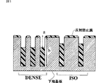
使用した基板は図1に示すようなホールのIsoとDenseパターンを有するシリコンウェハー基板である。Isoパターンは、ホール中心から隣のホール中心までの間隔が、当該ホールの直径の3倍であるパターンである。また、Denseパターンは、ホール中心から隣のホール中心までの間隔が、当該ホールの直径の1倍であるパターンである。ホールの深さは1.0μmであり、ホールの直径は0.20μmである。
実施例1〜4は、比較例1〜4に比べより要求特性を満たすことが明らかになった。これは、比較例1〜4の反射防止膜形成組成物に比べて、実施例1〜4の反射防止膜形成組成物のベースポリマーが、分子量が5000以下の高分子と、分子量が20000以上の高分子とを特定の比率で有する混合ポリマーであるためである。
本発明は、ホール基板上の塗布性制御を目的とした反射防止膜を形成する為の組成物である。得られた反射防止膜は、基板の反射防止効果だけでなく、エッチング工程やアッシング工程におけるホール底の材料保護に有効である。
本発明により、ホールやトレンチなどを有する凹凸の有る基板上の段差被覆性に優れ、レジスト層と比較して大きなドライエッチング速度を有し、反射光防止効果が高く、更にレジスト層とのインターミキシングが起こらず、加熱乾燥時にレジスト中への拡散物がなく、高解像力およびレジスト膜厚依存性に優れた反射防止膜材料用組成物を得ることができ、かつ優れたレジストパターン形成方法を提供することができる。
【図面の簡単な説明】
図1はホールを有する基板に反射防止膜形成組成物を塗布した状態の断面図である。aはホール中心での反射防止膜の凹み深さ(μm)である。また、bは使用した基板における当初のホールの深さ(μm)である。Technical field
The present invention is a novel anti-reflective coating material composition, more specifically, excellent coating control on uneven substrates such as holes and trenches, has a high anti-reflecting effect, and does not cause intermixing with a resist layer. The present invention provides an antireflection film for lithography that has an excellent resist pattern and has a higher dry etching rate than that of a resist. In particular, as a wiring material used in recent years to reduce the wiring delay of a semiconductor device. The present invention relates to an antireflection film for dual damascene process for introducing Cu (copper).
Background art
Conventionally, in the manufacture of semiconductor devices, fine processing by lithography using a photoresist composition has been performed. The fine processing was obtained by forming a thin film of a photoresist composition on a silicon wafer, irradiating with an actinic ray such as ultraviolet rays through a mask pattern on which a semiconductor device pattern was drawn, and developing it. This is a processing method of etching a silicon wafer using a resist pattern as a protective film. However, in recent years, higher integration of semiconductor devices has progressed, and actinic rays used tend to be shortened from i-line (365 nm) to KrF excimer laser (248 nm) and ArF excimer laser (193 nm). . Accordingly, the influence of diffuse reflection of active rays from the substrate and standing waves has been a serious problem. Therefore, a method of providing an antireflection film (Bottom Anti-Reflective Coating, BARC) between the photoresist and the substrate has been widely studied.
As an antireflection film, an inorganic antireflection film such as titanium, titanium dioxide, titanium nitride, chromium oxide, carbon, and α-silicon, and an organic antireflection film made of a light-absorbing substance and a polymer compound are known. The former requires equipment such as a vacuum deposition apparatus, a CVD apparatus, and a sputtering apparatus for film formation, whereas the latter is advantageous in that no special equipment is required, and many studies have been made. For example, an acrylic resin-type antireflection film having a hydroxyl group and a light-absorbing group in the same molecule as a crosslinking reaction group described in US Pat. No. 5,919,599, and a crosslinking reaction group described in US Pat. No. 5,693,691 Examples thereof include a novolak resin type antireflection film having a hydroxyl group and a light absorbing group in the same molecule.
Physical properties desired as an organic antireflection film material include a large absorbance to light and radiation, no intermixing with the resist layer (insoluble in the resist solvent), application or heating There are no low-molecular-weight diffused substances from the antireflection film material into the top coat resist during drying, and a large dry etching rate compared to the resist. SPIE, Vol. 3678, 800-809, Vol. 3678, 174-185 (1999) and Proc. SPIE, Vol. 2195, 225-229 (1994).
However, when the LSI pattern rule has a fineness of 0.13 μm or less, the influence of wiring delay on the speeding up of the LSI increases, and the performance enhancement of the LSI will be advanced by the current LSI process technology. Is getting harder. The materials used to reduce the wiring delay are the wiring material Cu and a low dielectric constant interlayer insulating film. A technique introduced to change the wiring material from current Al (aluminum) to Cu is a dual damascene process. In the dual damascene process, an antireflection film is used on a substrate having a larger aspect ratio (unevenness) than that of a conventional wiring material Al substrate.
The physical property required for the anti-reflection film for dual damascene process is to control the coating shape of the anti-reflection film on the underlying substrate around the hole. Regarding the control of the coating shape of the antireflection film on the underlying substrate around the hole, there are the following two methods and the antireflection film.
One method is a full-fill type, in which the antireflection film is used to completely fill the holes and planarize the substrate. This is desired to fill the hole with an antireflection film close to 100%. The advantage in this method is advantageous for the lithography process. However, it is disadvantageous to the etching process as a disadvantage.
Another method is a partial-fill type, in which the antireflection film fills part of the hole and covers the surface layer at the bottom of the hole and the top of the hole edge.
Here, it is desirable that the hole filling rate is close to 20 to 80%. The advantage of this method is that the hole filling amount of the antireflection film material is 20 to 80%, so that the process of removing the antireflection film by etching is performed in a short time compared to the case of the filling amount close to 100%. This is advantageous. However, the disadvantage is that the lithography process is disadvantageous in terms of the antireflection effect because the substrate having holes is not completely flattened. However, the use of the anti-reflection film of the full-fill type is mainly used in a highly integrated substrate portion having a wiring width of 0.2 μm or less, whereas the anti-reflection film of the partial fill type has a wiring width of 0.2 μm or less. Since it may be necessary to use with other anti-reflective coatings in order to use it on a highly integrated substrate part, it is usually used on a low integrated substrate with a wiring width of 0.3 μm or more. Is done.
As required characteristics of the antireflection film forming material used in this partial fill type, it is important that the antireflection film has the following performance when the antireflection film is applied with a constant film thickness.
(1) The filling amount of the antireflection film in the hole is 20 to 80%, preferably 30 to 70% with respect to the volume per hole.
(2) The antireflection film filled in the hole should not have air voids or gaps.
(3) The antireflection film should not adhere to the side wall of the hole.
(4) The upper part of the hole edge is covered with an antireflection film.
(5) The thickness of the antireflection film is constant regardless of the density of holes on the substrate.
(6) Do not perform resist poisoning.
There is a need for an antireflection coating that satisfies these six performances.
In particular, when an antireflection film is applied with a constant film thickness, the filling rate of the antireflection film in the hole is 20 to 80%, preferably 30 to 70%. Air voids and gaps are formed in the hole. There is a need for an antireflection film material in which the film thickness of the antireflection film is constant, regardless of whether it is present or the density of holes on the substrate.
As an example of using a conventional antireflection film forming material used in a partial fill type, for example, JP 2000-294504 A is a method of forming a photoresist relief image on a substrate having a topography, (A) applying a layer of an antireflective composition comprising a polymer having a molecular weight of about 8000 or less on the substrate, (b) applying a layer of a photoresist composition over the antireflective composition layer, and ( c) A method of forming a photoresist relief image comprising exposing a photoresist layer with activating radiation and developing the exposed photoresist layer. Among them, in a preferred embodiment, the antireflective composition is formed by local oxidation of silicon and has a slope shape that is 0.8 microns wide and 2 microns midpoint depth of about 0.5 or more. It is said that it is the method of showing the flatness of the. However, the above publication is an important point in the case where an antireflection film forming material is used in the partial fill type, with respect to the formation of air voids and gaps that are likely to hinder the effect when an antireflection film is applied. No mention is made, and there is no description as to whether the thickness of the antireflection film is constant regardless of the density of the holes on the substrate.
An object of the present invention is that when an antireflection film is applied with a constant film thickness, the filling rate of the antireflection film is 20 to 80% in the hole, and there are no air voids or gaps in the hole. Regardless of the density of holes on the substrate, the thickness of the antireflection film is constant, the antireflection effect is high, intermixing with the resist layer does not occur, and an excellent resist pattern is obtained. An object of the present invention is to provide an antireflection film for lithography having a higher dry etching rate than that of the above, and to provide a method for forming a resist pattern using the antireflection film forming composition.
That is, the polymer disclosed in the present invention and the composition for forming an antireflection film using the polymer have high antireflection properties by completely filling the holes on the substrate and flattening them so that the wiring width is relatively narrow. Rather than applying to a full-fill type anti-reflection film used to determine the performance, the partial-fill type anti-reflection is used to obtain a high dry etching rate as well as an anti-reflective capability applied to a relatively wide wiring width. More suitable for application to membranes.
Disclosure of the invention
The present invention provides, as a first aspect, an antireflection film-forming composition comprising a polymer (A) having a weight average molecular weight of 5000 or less and a polymer (B) having a weight average molecular weight of 20000 or more,
As a second aspect, the antireflection film-forming composition according to the first aspect, in which the polymer (A) is a halogenated bisphenol A resin having a weight average molecular weight of 700 to 5,000,
As a third aspect, the halogenated bisphenol A resin has at least the formula (1):
As a fourth aspect, the antireflection film-forming composition according to the first aspect, in which the polymer (A) is a halogen-containing novolak resin having a weight average molecular weight of 600 to 5,000,
As a fifth aspect, the halogen-containing novolak resin has at least the formula (3):
As a sixth aspect, the antireflection film formation according to any one of the first to fifth aspects, in which the polymer (B) is a polyacrylic acid ester or a polymethacrylic acid ester having a weight average molecular weight of 20000 to 200000. Composition,
As a seventh aspect, the antireflection film-forming composition according to any one of the first to fifth aspects, wherein the polymer (B) is polystyrene or a derivative thereof having a weight average molecular weight of 20000 to 200000,
As an eighth aspect, any one of the first to seventh aspects, containing 33.7 to 83.2% by weight of the polymer (A) and 66.3 to 16.8% by weight of the polymer (B). An antireflective film forming composition according to one of the above,
As a ninth aspect, the antireflection film-forming composition according to any one of the first to eighth aspects, further comprising a crosslinking agent having at least two crosslink-forming functional groups,
As a tenth aspect, it is used in the manufacture of a semiconductor device by a method of coating a photoresist on a substrate having a hole having an aspect ratio of 1 or more represented by height / diameter and transferring an image onto the substrate using a lithography process. The antireflection film-forming composition according to any one of the first to ninth aspects, used to partially fill holes in the substrate before coating with a photoresist,
As an eleventh aspect, the antireflection film-forming composition according to the tenth aspect, in which filling of holes on the substrate is 20 to 80% of the volume per hole, and
As a 12th viewpoint, the following (I) process, (II) process, and (III) process:
Step (I): Applying the antireflection film-forming composition according to any one of the first to ninth aspects to a substrate having holes having an aspect ratio of 1 or more represented by height / diameter, followed by drying. A step of filling 20 to 80% of the hole volume on the substrate with an antireflection film,
(II) step: a step of applying a resist and drying, and
(III) Step: A method of manufacturing a semiconductor device in which an image is transferred onto a substrate comprising exposure, development, and etching, and an integrated circuit element is formed.
The present invention is an antireflection film-forming composition used in a lithography process for manufacturing a semiconductor device, comprising a polymer (A) having a weight average molecular weight of 5000 or less and a polymer (B) having a weight average molecular weight of 20000 or more. As the polymer, those containing a halogen atom in the main chain can be preferably used.
The polymer (A) having a molecular weight of 5000 or less that forms the antireflection film of the present invention varies depending on the coating solvent used, solution viscosity, film shape, etc., but novolak resin, bisphenol A type resin, polyester resin, and polyether resin Etc. can be preferably used.
The polymer (B) having a molecular weight of 20000 or more which forms the antireflection film of the present invention varies depending on the coating solvent used, the solution viscosity, the film shape, etc., but acrylic resin, polyester resin, polyvinylphenol resin, polyimide resin, etc. It can be preferably used.
Among them, the polymer is particularly preferably composed of a halogen-containing novolak resin and / or a derivative thereof, and an acrylic resin and / or a derivative thereof.
The weight ratio of the polymer in the obtained antireflection film is such that the polymer (A) having a molecular weight of 5000 or less is 33.7 to 83.2% by weight, and the polymer (B) having a molecular weight of 20000 or more is 16.8 to 66.3. The polymer (A) having a molecular weight of 5000 or less is preferably 50.0-75.0% by weight, and the polymer (B) having a molecular weight of 20000 or more is 25.0-50.0% by weight.
The antireflection film-forming composition of the present invention contains the above polymer and solvent, and may further contain a crosslinking agent, other additives, and the like. The solid content of the antireflection film-forming composition of the present invention is 0.1 to 50% by weight. And as content of the said polymer, it is 0.1-50 weight part with respect to 100 weight part of all compositions, Preferably it is 1-30 weight part.
The polymer in the present invention may be any of a random copolymer, a block copolymer, or a graft copolymer. The polymer forming the antireflection film of the present invention can be synthesized by methods such as radical polymerization, anionic polymerization, and cationic polymerization. The form can be various methods such as solution polymerization, suspension polymerization, emulsion polymerization and bulk polymerization.
As the polymer (A), for example, a halogenated bisphenol A type resin having a weight average molecular weight of 700 to 5,000 can be used.
The halogenated bisphenol A type resin is preferably a polymer represented by at least the formula (1).
Halogenated bisphenol A resin can be synthesized by polycondensation of halogenated bisphenol A and epichlorohydrin. Examples of the halogenated bisphenol A include tetrabromobisphenol A and tetrachlorobisphenol A, and commercially available products having a halogen content of 46 to 52% and an epoxy equivalent of 330 to 700 g / eq can be easily obtained. .
An end of the halogenated bisphenol A resin has an epoxy group, and at least one of the epoxy groups can be reacted with a compound that reacts with the epoxy group.
The terminal structure of the halogenated bisphenol A resin is preferably a structure of the formula (2) having a light absorbing portion.
In the formula (1), X 1 Represents a halogen atom such as a bromine atom or a chlorine atom. n1 represents the number of repeating units and is 1 to 50, preferably 1 to 10. n2 and n3 represent the number of halogen atoms substituted on the benzene ring, and n2 and n3 are each a number of 1 to 3, but preferably n2 and n3 are 2.
In the formula (2), P represents an (n4 + 1) -valent aromatic ring group having 6 to 14 carbon atoms. For example, a light absorbing group such as a benzene ring, a naphthalene ring, and an anthracene ring can be exemplified.
M represents an electron donating group. M is -OH, -OR 2 , -R 2 , -N (R 3 ) (R 4 ) Or -SR 4 And substituents such as R 2 Represents a hydrocarbon group having 1 to 20 carbon atoms, R 3 , R 4 May be the same or different and each represents a hydrogen atom or a hydrocarbon group having 1 to 20 carbon atoms. Examples of M include a methyl group, an ethyl group, a butyl group, a hydroxyl group, a methoxy group, an ethoxy group, an allyl group, a vinyl group, and an amino group. n4 represents the number of substitutions of M for P. n4 is an integer from 0 to 3. When n4 is 2 to 3, M may be the same or different.
At least one of the epoxy groups at both ends of the halogenated bisphenol A resin reacts with an aromatic compound such as an aromatic organic acid, aromatic amine, aromatic alcohol, etc. It is necessary to take the structure of the formula (2) at Y of As these aromatic compounds, compounds having a structure in which one or more functional groups such as a carboxyl group, a sulfonic acid group, an amino group, and a hydroxyl group are substituted on an aromatic ring such as a benzene ring, a naphthalene ring, and an anthracene ring Can be used. These are aromatic compounds having absorptivity in the ultraviolet region, such as benzoic acid, benzenesulfonic acid, aniline, benzylamine, phenol, naphthalenecarboxylic acid, naphthylacetic acid, naphthalenesulfonic acid, naphthylamine, naphthol, anthracenecarboxylic acid, Anthracene sulfonic acid, aminoanthracene, hydroxyanthracene, and derivatives thereof may be mentioned. When these aromatic compounds and halogenated bisphenol A type resin are reacted and the Y portion takes a structure represented by the formula (2), it is a divalent linking group (T 1 ) Is —O—CO—, —SO 2 A structure such as —O—, —NH—, —O— and the like is shown.
Among the aromatic compounds, 9-anthracene carboxylic acid is particularly preferable. When 9-anthracene carboxylic acid is used, in formula (2) (T 1 ) Represents —O—CO—, and (P) represents an anthryl group.
One of the epoxy groups at both ends of the halogenated bisphenol A resin can react with an aliphatic organic acid, aliphatic alcohol, aliphatic amine or water. By reacting these, the formula (4):
Depending on the reaction conditions, one of the epoxy groups at both ends of the halogenated bisphenol A resin may be present in an unreacted state. In that case, in formula (4), Y is formula (5):
Accordingly, the halogenated bisphenol A type resin used in the present invention has the structures of the formulas (2), (5) and (6) in the formula (4). In these Y, when the total number of moles of repeating units of Formula (2), Formula (5) and Formula (6) is 1, the formula (2): Formula (5): Formula (6) values are respectively In the range of 0.5 to 1.0: 0 to 0.5: 0 to 0.5, preferably 0.8 to 1.0: 0 to 0.2: 0. The range is 0.2.
The halogenated bisphenol A resin used in the present invention is obtained by reacting an epoxy group at both ends with 9-anthracenecarboxylic acid (7):
Similarly, the formula (8):
In the structure of the halogenated bisphenol A resin, a hydroxyl group reacts with a crosslinking-forming functional group in the crosslinking agent, whereby a crosslinked structure can be formed in the antireflection film.
It is essential that at least one Y has the structure of the formula (2) by reacting an aromatic compound having a light absorbency with an epoxy group present at the terminal of the halogenated bisphenol A resin. When Y at both ends has the structure of formula (2), one Y is formula (2) and the other Y is formula (5), and one Y is formula (2) and the other There is a case where Y in Formula (6).
In the present invention, when an antireflection film is formed by containing a halogen atom having a large atomic weight, particularly bromine atom, the dry etching rate is high, but the ratio of light absorbing groups per unit weight of the antireflection film forming material is increased. Therefore, it is preferable that the proportion of Y in the halogenated bisphenol A type resin is the formula (2) is large.
The halogenated bisphenol A type resin is obtained by polymerization of halogenated bisphenol A such as tetrabromobisphenol A and chloromethyloxirane such as epichlorohydrin.
In addition, as the polymer (A), for example, a halogen-containing novolac resin having a weight average molecular weight of 700 to 5000 can be used.
The halogen-containing novolak resin is a polymer having at least a repeating unit of the formula (3).
The halogen-containing novolac resin includes the formula (3) and the formula (9):
As the halogen-containing novolak resin, a halogen-containing novolak resin having an epoxy group represented by the formula (9) is prepared, and a compound that reacts with the epoxy group is added to the halogen-containing novolak resin, thereby formulas (3) and (10) It can be easily produced by a method of converting to a part having a repeating unit of At this time, a resin having a repeating unit of the formula (3) and the formula (10) is generated by using at least one compound that reacts with the epoxy group.
The repeating unit of formula (3) is a portion where a light-absorbing substance is bonded, and the light-absorbing substance is added to the resin of formula (9) to obtain the repeating unit of formula (3). Examples of the light-absorbing substance include those in which a benzene ring, naphthalene ring, anthracene ring, or pyrene ring is substituted with one or more functional groups such as a carboxyl group, a sulfonic acid group, an amino group, and a hydroxyl group. In addition, these are further -OR 2 , -N (R 3 ) (R 4 ) Or -SR 4 (Where R 2 Represents a hydrocarbon group having 1 to 20 carbon atoms, R 3 , R 4 May be the same or different and each represents a hydrogen atom or a hydrocarbon group having 1 to 20 carbon atoms. ) May be substituted.
When these light-absorbing substances react with the epoxy group of formula (9), they are divalent linking groups (T 2 ) Is —O—CO—, —SO 2 A structure such as —O—, —NH— or —O— is shown.
The light-absorbing substance preferably has a carboxyl group or a functional group that can be converted into a carboxyl group, and is reacted with an epoxy group of the formula (9) to be linked. This carboxyl group or a functional group that can be converted to a carboxyl group is added to an epoxy group present in the resin of the formula (9) to produce a resin having a repeating unit of the formula (3). As a particularly preferred light-absorbing substance, 9-anthracenecarboxylic acid can be mentioned, and the formula (11):
When 9-anthracenecarboxylic acid is used, in the structure of formula (3) (T 2 ) Represents —O—CO—, and (P) represents an anthryl group.
A light-absorbing substance having a carboxyl group or a functional group that can be converted into a carboxyl group is subjected to an addition reaction with the resin having a repeating unit of formula (9) to produce a resin having a repeating unit of formula (3). At this time, the remaining epoxy group of the resin having a repeating unit of the formula (9) undergoes hydrolysis, and a repeating unit of the formula (10) (Z = —OH) to which a hydroxyl group is added can also be generated.
Moreover, the repeating unit of Formula (3) and Formula (10) is also the part which couple | bonded the crosslinking reaction group (hydroxyl group).
The repeating units of the formulas (3) and (10) are structural units that bring about light absorbance and control the rate of crosslinking reaction with the crosslinking agent. That is, the crosslinking reaction rate can be controlled by changing the number of moles of each repeating unit of the formulas (3) and (10) when the total number of moles of repeating units is 1.
In formula (3), formula (9) and formula (10), the number of moles of each repeating unit when the total number of moles of repeating units of formula (3), formula (9) and formula (10) is 1. , N8: n9: n5 = 0 to 0.8: 0 to 0.8: 0.2-1 molar ratio, preferably n8: n9: n5 = 0 to 0.2: 0 to 0.2. : A molar ratio of 0.8 to 1, more preferably n8: n9: n5 = 0 to 0.1: 0 to 0.1: 0.9 to 1 in a molar ratio of n8 + n9 + n5 = 1. Have.
In formula (11), n10: n11: n12 = 0 to 0.8: 0 to 0 in terms of the number of moles of each repeating unit when the total number of moles of repeating units constituting the resin is 1. .8: 0.2-1 molar ratio, preferably n10: n11: n12 = 0-0.2: 0-0.2: 0.8-1 molar ratio, more preferably n10: n11: n12 = It is contained in a molar ratio of 0 to 0.1: 0 to 0.1: 0.9 to 1, and has a structure of n10 + n11 + n12 = 1.
In order to add a light-absorbing substance to a halogen-containing novolak resin having an epoxy group represented by the formula (9), the repeating unit of the formula (3) is essential, but the light-absorbing substance is an epoxy group of the formula (9). In the case of addition reaction over all of the above, the repeating unit of formula (9) is zero. The structural unit consisting of the formula (3), the formula (9) and the formula (10) is generated when the total number of moles of the repeating units of the formula (3), the formula (9) and the formula (10) is 1. It is represented by the ratio of each repeating unit when the total number of moles of repeating units of each monomer constituting the resin is 1.
In the present invention, since a resin containing a halogen atom having a large atomic weight, particularly a bromine atom, is used, when an antireflection film-forming material containing these resins is applied, the absorption group per unit weight of the antireflection film-forming material is reduced. In order to increase the ratio, it is necessary to contain a large number of repeating units of the formula (3) in the structure.
A resin of the formula (12) obtained by adding only a light-absorbing substance to all or part of the epoxy group of the resin of the formula (9) and converting it into a repeating unit of the formula (3) can be preferably used.
In addition, in the resin of the formula (12), the resin of the formula (13) obtained by producing under the condition that hydrolysis does not occur can be preferably used.
The resin of the above formula (3) is obtained by mixing the resin of formula (9) and the light-absorbing substance in a solvent such as propylene glycol monomethyl ether or propylene glycol monomethyl ether acetate, such as benzyltriethylammonium chloride or tetramethylammonium hydroxide. It is synthesized by performing a reaction at 100 to 130 ° C., normal pressure, and 12 to 48 hours using a catalyst.
The polymer (B) used in the present invention has a weight average molecular weight of 20000 or more. A light-absorbing substance corresponding to the above P can be bound to the polymer (B). For example, a light-absorbing substance corresponding to P can be added to a structural unit having a glycidyl group to obtain a polymer (B) having a light-absorbing site. However, the polymer (B) does not necessarily have an absorption site.
The polymer (B) needs to have a crosslinking-forming functional group such as a hydroxyl group, and can be obtained by polymerizing a monomer having a hydroxyl group or polymerizing a monomer having a functional group that generates a hydroxyl group by reaction.
As the polymer (B), for example, an acrylic ester or a methacrylic ester having a weight average molecular weight of 20,000 to 200,000 can be used.
As the poly (meth) acrylic acid ester as the polymer (B), for example, a poly (meth) acrylic acid ester having a hydroxyalkyl group or a poly (meth) acrylic acid ester having an epoxy group can be used.
For example, hydroxymethyl methacrylate, hydroxyethyl methacrylate, hydroxypropyl methacrylate, hydroxybutyl methacrylate, hydroxypentyl methacrylate, hydroxyphenyl methacrylate, hydroxypropyl acrylate, glycidyl acrylate, glycidyl methacrylate, etc. can be polymerized alone, or two or more of these It is obtained by copolymerizing monomers.
Examples of the polymer (B) used in the present invention include polystyrene having a weight average molecular weight of 20,000 to 200,000 or a derivative thereof. In these resins, polyhydroxystyrene having a functional group such as a hydroxyl group capable of forming a crosslinking bond with a crosslinking agent can be used.
In the polymer (B), it is possible to copolymerize monomers other than those, thereby finely adjusting the crosslinking reaction rate, the dry etching rate, the reflectance, and the like. Examples of such a copolymerization monomer include the following. For example, acrylic acid, methacrylic acid, maleic acid, fumaric acid, acrylic acid esters, acrylamides, methacrylic acid esters, methacrylamides, allyl compounds, vinyl ethers, vinyl esters, styrenes, crotonic acid esters, etc. It is a compound having one selected addition polymerizable unsaturated bond.
Examples of the acrylates include alkyl acrylates having 1 to 10 carbon atoms in the alkyl group.
Examples of the methacrylic acid esters include alkyl methacrylates having 1 to 10 carbon atoms in the alkyl group.
Acrylamides include acrylamide, N-alkyl acrylamide, N-aryl acrylamide, N, N-dialkyl acrylamide, N, N-aryl acrylamide, N-methyl-N-phenyl acrylamide, N-2-acetamidoethyl-N-. Examples include acetylacrylamide.
Examples of the methacrylamides include methacrylamide, N-alkylmethacrylamide, N-arylmethacrylamide, N, N-dialkylmethacrylamide, N, N-diarylmethacrylamide, N-methyl-N-phenylmethacrylamide, N- Examples include ethyl-N-phenylmethacrylamide.
Examples of vinyl ethers include alkyl vinyl ethers and vinyl aryl ethers.
Examples of vinyl esters include vinyl butyrate, vinyl isobutyrate, and vinyl trimethyl acetate.
Examples of styrenes include styrene, alkyl styrene, alkoxy styrene, halogenated styrene, and carboxy styrene.
Examples of the crotonic acid esters include alkyl crotonates such as butyl crotonate, hexyl crotonate, and glycerin monocrotonate.
Further, dialkyl itaconates, dialkyl esters or monoalkyl esters of maleic acid or fumaric acid, maleimide, acrylonitrile, methacrylonitrile, maleilonitrile and the like can be mentioned. In addition, generally, any addition-polymerizable unsaturated compound can be used.
The antireflection film-forming composition of the present invention can contain a cross-linking agent having at least two cross-linking functional groups. Examples of the crosslinking agent include melamine-based, substituted urea-based, and polymer-based polymers containing epoxy groups. A compound such as methoxymethylated glycoluril or methoxymethylated melamine is preferable, and tetramethoxymethylglycoluril or hexamethoxymethylmelamine is particularly preferable. The addition amount of the crosslinking agent varies depending on the coating solvent used, the base substrate used, the required solution viscosity, the required film shape, etc., but is 0.001 to 20 parts by weight with respect to 100 parts by weight of the total composition. The amount is preferably 0.01 to 10 parts by weight, more preferably 0.1 to 5.0 parts by weight.
In the antireflection film composition of the present invention, p-toluenesulfonic acid, trifluoromethanesulfonic acid, pyridinium p-toluenesulfonic acid, salicylic acid, sulfosalicylic acid, citric acid, benzoic acid, hydroxybenzoic acid are used as a catalyst for promoting the crosslinking reaction. An acidic compound such as an acid or / and a thermal acid generator such as 2,4,4,6-tetrabromocyclohexadienone, benzoin tosylate, 2-nitrobenzyl tosylate can be blended. The amount is 0.02 to 10 parts by weight, preferably 0.04 to 5 parts by weight, per 100 parts by weight of the total solid content.
In addition to the above, the composition for forming an antireflective film of the present invention may contain additional light absorbers, rheology modifiers, adhesion aids, surfactants, and the like as necessary.
Examples of further light absorbers include commercially available light absorbers described in “Technical dye technology and market” (published by CMC) and “Dye Handbook” (edited by the Society of Synthetic Organic Chemistry), such as C.I. I. Disperse Yellow 1, 3, 4, 5, 7, 8, 13, 23, 31, 49, 50, 51, 54, 60, 64, 66, 68, 79, 82, 88, 90, 93, 102, 114 and 124 C. I. Disperse
The rheology modifier is added mainly for the purpose of improving the fluidity of the antireflective film-forming composition, and particularly for enhancing the filling property of the antireflective film-forming composition into the holes in the baking process. Specific examples include phthalic acid derivatives such as dimethyl phthalate, diethyl phthalate, diisobutyl phthalate, dihexyl phthalate, and butyl isodecyl phthalate; adipic acid derivatives such as dinormal butyl adipate, diisobutyl adipate, diisooctyl adipate, and octyl decyl adipate; Mention may be made of maleic acid derivatives such as normal butyl maleate, diethyl maleate and dinonyl maleate, oleic acid derivatives such as methyl oleate, butyl oleate and tetrahydrofurfuryl oleate, or stearic acid derivatives such as normal butyl stearate and glyceryl stearate. it can. These rheology modifiers are usually blended in a proportion of less than 30 parts by weight with respect to 100 parts by weight of the total composition of the antireflection film for lithography.
The adhesion auxiliary agent is added mainly for the purpose of improving the adhesion between the substrate or the resist and the antireflection film-forming composition and preventing the resist from peeling particularly during development. Specific examples include chlorosilanes such as trimethylchlorosilane, dimethylvinylchlorosilane, methyldiphenylchlorosilane, chloromethyldimethylchlorosilane, trimethylmethoxysilane, dimethyldiethoxysilane, methyldimethoxysilane, dimethylvinylethoxysilane, diphenyldimethoxysilane, Alkoxysilanes such as enyltriethoxysilane, hexamethyldisilazane, N, N′-bis (trimethylsilyl) urea, silazanes such as dimethyltrimethylsilylamine, trimethylsilylimidazole, vinyltrichlorosilane, γ-chloropropyltrimethoxysilane, γ -Silanes such as aminopropyltriethoxysilane and γ-glycidoxypropyltrimethoxysilane, benzotriazole, benzimidazole , Indazole, imidazole, 2-mercaptobenzimidazole, 2-mercaptobenzothiazole, 2-mercaptobenzoxazole, urazole, thiouracil, mercaptoimidazole, mercaptopyrimidine, etc., 1,1-dimethylurea, 1,3- Mention may be made of urea such as dimethylurea or thiourea compounds. These adhesion assistants are usually blended in a proportion of less than 5 parts by weight, preferably less than 2 parts by weight, based on 100 parts by weight of the total composition of the antireflection film for lithography.
In the antireflection film-forming composition of the present invention, there is no occurrence of pinholes or setups, and a surfactant can be blended in order to further improve the applicability to surface unevenness. Examples of the surfactant include polyoxyethylene lauryl ether, polyoxyethylene stearyl ether, polyoxyethylene cetyl ether, polyoxyethylene alkyl ethers such as polyoxyethylene oleyl ether, polyoxyethylene octylphenol ether, polyoxyethylene nonyl Polyoxyethylene alkyl allyl ethers such as phenol ether, polyoxyethylene / polyoxypropylene block copolymers, sorbitan monolaurate, sorbitan monopalmitate, sorbitan monostearate, sorbitan monooleate, sorbitan trioleate, sorbitan tristearate Sorbitan fatty acid esters such as rate, polyoxyethylene sorbitan monolaurate, polyoxyethylene sol Nonionic surfactants such as polyoxyethylene sorbitan fatty acid esters such as tan monopalmitate, polyoxyethylene sorbitan monostearate, polyoxyethylene sorbitan trioleate, polyoxyethylene sorbitan tristearate, EFTTOP EF301, EF303, EF352 (Manufactured by Tochem Products Co., Ltd.), MegaFac R08, R30, LS-14 (Dainippon Ink Chemical Co., Ltd.), Florad FC430, FC431 (Sumitomo 3M Co., Ltd.), Asahi Guard AG710, Surflon S-382 SC101, SC102, SC103, SC104, SC105, SC106 (manufactured by Asahi Glass Co., Ltd.), etc., organosiloxane polymer KP341 (manufactured by Shin-Etsu Chemical Co., Ltd.), etc. Can. The compounding amount of these surfactants is usually 1 part by weight or less, preferably 0.5 parts by weight or less per 100 parts by weight of the total composition of the present invention. These surfactants may be added alone or in combination of two or more.
In the present invention, the solvent for dissolving the resin includes ethylene glycol monomethyl ether, ethylene glycol monoethyl ether, methyl cellosolve acetate, ethyl cellosolve acetate, diethylene glycol monomethyl ether, diethylene glycol monoethyl ether, propylene glycol, propylene glycol monomethyl ether, propylene Glycol monomethyl ether acetate, propylene glycol propyl ether acetate, toluene, xylene, methyl ethyl ketone, cyclopentanone, cyclohexanone, ethyl 2-hydroxypropionate, ethyl 2-hydroxy-2-methylpropionate, ethyl ethoxy acetate, ethyl hydroxyacetate, 2 -Methyl hydroxy-3-methylbutanoate, 3-methoxy It is possible to use methyl propionate, ethyl 3-methoxypropionate, ethyl 3-ethoxypropionate, methyl 3-ethoxypropionate, methyl pyruvate, ethyl pyruvate, ethyl acetate, butyl acetate, ethyl lactate, butyl lactate, etc. it can. These organic solvents are used alone or in combination of two or more.
Furthermore, high boiling point solvents such as propylene glycol monobutyl ether and propylene glycol monobutyl ether acetate can be mixed and used. Among these solvents, propylene glycol monomethyl ether, propylene glycol monomethyl ether acetate, ethyl lactate, butyl lactate, and cyclohexanone are preferable for improving the leveling property.
As the resist applied to the upper layer of the antireflection film in the present invention, either a negative type or a positive type can be used, a positive type resist comprising a novolak resin and 1,2-naphthoquinonediazide sulfonic acid ester, a photoacid generator and an acid. Amplification resist consisting of a binder having a group that degrades by alkali and increases the alkali dissolution rate, chemical amplification consisting of a low molecular weight compound that increases the alkali dissolution rate of the resist by decomposition with an alkali soluble binder, a photoacid generator and an acid Type resist, a chemically amplified resist composed of a low-molecular compound that decomposes with a photoacid generator and an acid to increase the alkali dissolution rate and a low molecular compound that decomposes with an acid to increase the alkali dissolution rate, For example, the product name APEX-E manufactured by Shipley is available.
As a developer of a positive photoresist having an antireflection film for lithography formed using the antireflection film-forming composition of the present invention, sodium hydroxide, potassium hydroxide, sodium carbonate, sodium silicate, sodium metasilicate Inorganic alkalis such as ammonia water, primary amines such as ethylamine and n-propylamine, secondary amines such as diethylamine and di-n-butylamine, tertiary amines such as triethylamine and methyldiethylamine, dimethylethanolamine Alcohol amines such as triethanolamine, quaternary ammonium salts such as tetramethylammonium hydroxide, tetraethylammonium hydroxide, choline, cyclic amines such as pyrrole and piperidine, etc. it can. Furthermore, an appropriate amount of an alcohol such as isopropyl alcohol or a nonionic surfactant may be added to the alkaline aqueous solution. Of these, preferred developers are quaternary ammonium salts, more preferably tetramethylammonium hydroxide and choline.
A method for manufacturing a semiconductor device using the antireflection material of the present invention includes the following steps (I), (II) and (III):
Step (I): The above-described antireflection film-forming composition is applied to a substrate having holes having an aspect ratio of 1 or more represented by height / diameter, and dried to give 20 to 80 of the hole volume on the substrate. %, Preferably 30-70% is filled with an antireflection film,
(II) step: a step of applying a resist and drying, and
(III) Process: It consists of the process of transferring an image onto a substrate comprising exposure, development and etching, and forming an integrated circuit element. The conditions for baking after application of the antireflection film composition are 80 to 250 ° C. and 1 to 120 minutes.
As described above, the antireflection film-forming material of the present invention is a lithographic process in which a photoresist is coated on a substrate having holes having an aspect ratio of 1 or more, usually 1 to 50 in terms of height / diameter. It is used in the manufacture of a semiconductor device by a method of transferring an image onto a substrate by using, and can be used to partially fill holes in the substrate before coating with a photoresist.
The antireflection film-forming composition of the present invention can control the crosslinking reaction rate by adding a halogen having a relatively large atomic volume in the vicinity of the hydroxyl group that is a crosslinking reaction group. In the case of an antireflection film-forming composition in which an aromatic hydrocarbon that decreases the crosslinking reaction rate is added in the vicinity of the crosslinking reaction group instead of the halogen atom, it is difficult to obtain a large dry etching rate compared to the resist. is there. The antireflection film-forming composition using the halogen-containing resin can moderately suppress the cross-linking reaction rate, obtain high flatness, and at the same time reduce the concentration of carbon atoms in the composition. It has the characteristic that a large dry etching rate can be obtained as compared with the resist.
In addition, the antireflection film-forming composition of the present invention has a light absorption part linked to the polymer resin side chain, so that there is no diffusion into the resist during heating and drying, and the light absorption part has a sufficiently large extinction coefficient. Because it has a high anti-reflected light effect, the content (weight fraction) of cyclic carbon such as an aromatic ring contained in the light-absorbing part is small, so even if the amount of addition of the light-absorbing part is increased, it can be dried. Less decrease in etching rate.
Furthermore, the antireflection film-forming composition of the present invention has a function of preventing reflection of light depending on process conditions, and further prevents the interaction between the substrate and the resist or at the time of exposure to the material or resist used in the resist. It can be used as a film having a function of preventing an adverse effect of a substance to be generated on a substrate.
In addition, when the coating property of the antireflection film of the present invention is used as a film having more excellent flatness, the glass transition temperature (Tg) of the light-absorbing polymer is slightly lowered, and some flow occurs during baking. There is a method of making it insoluble in a resist solvent after it is completely hardened. For this purpose, it is conceivable to slightly reduce the crosslinking function of the light-absorbing polymer due to heat. In order to achieve such a planarization function, the degree of polymerization of the light absorbing polymer, the concentration of the light absorbing polymer in the composition, the selection of the repeating unit, the substituent of the repeating unit, and the selection and addition of the comonomer Various methods such as selection of components are conceivable.
BEST MODE FOR CARRYING OUT THE INVENTION
Hereinafter, the present invention will be described in more detail with reference to examples.
Synthesis example 1
A halogen-containing novolac epoxy resin (manufactured by Nippon Kayaku Co., Ltd., trade name BREN-304) was prepared. The weight average molecular weight is 900, and the structure is represented by formula (14).
Synthesis example 2
After dissolving 26 g of glycidyl methacrylate monomer and 57 g of hydroxypropyl methacrylate in 331 g of propylene glycol monomethyl ether, nitrogen was purged into the reaction solution for 30 minutes. While maintaining the reaction solution at 70 ° C., 0.8 g of azobisisobutyronitrile AIBN as a polymerization initiator and 0.3 g of 1-dodecanethiol as a chain transfer agent were added and stirred under a nitrogen atmosphere. After stirring for 24 hours, 0.1 g of 4-methoxyphenol was added as a polymerization terminator. When GPC analysis of the obtained resin was performed, the weight average molecular weight was 36400 in terms of standard polystyrene. The solid content in the solution was 20%.
The structure of the obtained resin was a copolymer of glycidyl methacrylate and hydroxypropyl methacrylate corresponding to the formula (16), and had a molar ratio of m: n = 35: 65.
300 g of a polymer solution (manufactured by Lancaster) in which p-hydroxystyrene monomer was dissolved at a solid content concentration of 20% by weight in propylene glycol was used as a reaction solution. Nitrogen was purged through the reaction for 30 minutes. While maintaining the reaction solution at 70 ° C., 0.1 g of azobisisobutyronitrile AIBN was added as a polymerization initiator and stirred under a nitrogen atmosphere. The reaction product was obtained as a powder by filtering the precipitate obtained by reprecipitation in 1 liter of distilled water and drying. When the GPC analysis of the obtained polymer was conducted, the weight average molecular weight was 21000 in standard polystyrene conversion. The structure of the obtained polymer was poly p-vinylphenol corresponding to the formula (18).
Brominated bisphenol A type epoxy resin (product of Toto Kasei Co., Ltd., trade name YDB-400) was prepared. The weight average molecular weight is 1200, and the structure is represented by formula (19).
To 35.0 g of the solution having 13.6 g of the novolak resin obtained in Synthesis Example 1, 33.9 g of the solution having 6.8 g of the acrylic resin obtained in Synthesis Example 2 and 4.5 g of hexamethoxymethylmelamine as a crosslinking agent , 0.138 g of pyridinium p-toluenesulfonic acid as a curing agent and 0.30 g of R-30 (manufactured by Dainippon Ink & Chemicals, Inc.) as a surfactant are mixed, and 292.2 g of ethyl lactate as a solvent, propylene glycol monomethyl After dissolving in 137.6 g of ether and 53.1 g of cyclohexanone to obtain a 4.5% solution, the solution was filtered using a polyethylene microfilter having a pore size of 0.10 μm, and then using a polyethylene microfilter having a pore size of 0.05 μm. And filtered to prepare an antireflection film-forming composition. This solution was applied onto a silicon wafer using a spinner. An antireflection film (film thickness: 0.080 μm) was formed by heating on a hot plate at 205 ° C. for 1 minute.
The polymer of the obtained antireflection film had a ratio of 66.7% by weight of a novolak resin having a weight average molecular weight of 5000 or less and 33.3% by weight of an acrylic resin having a weight average molecular weight of 20000 or more. As a result of measuring this antireflection film with a spectroscopic ellipsometer, the refractive index n at 248 nm was 1.61, and the optical absorption coefficient k was 0.51.
Example 2
35.0 g of the solution containing 13.6 g of the bisphenol A resin obtained in Synthesis Example 4 above, 33.9 g of the solution containing 6.8 g of the acrylic resin obtained in Synthesis Example 2, and 4. 4-methoxyhexamethylmelamine as a cross-linking agent. 5 g, 0.138 g of pyridinium p-toluenesulfonic acid as a curing agent, 0.30 g of R-30 as a surfactant, and 292.2 g of ethyl lactate as a solvent, 137.6 g of propylene glycol monomethyl ether, and 53 of cyclohexanone 53 After dissolving in 1 g to make a 4.5% solution, the solution is filtered using a polyethylene microfilter having a pore size of 0.10 μm, and then filtered using a polyethylene microfilter having a pore size of 0.05 μm to form an antireflection film. A composition was prepared. This solution was applied onto a silicon wafer using a spinner. An antireflection film (film thickness: 0.080 μm) was formed by heating on a hot plate at 205 ° C. for 1 minute.
The polymer of the obtained antireflection film had a ratio of 66.7% by weight of a bisphenol A type resin having a weight average molecular weight of 5000 or less and 33.3% by weight of an acrylic resin having a weight average molecular weight of 20000 or more. As a result of measuring this antireflection film with a spectroscopic ellipsometer, the refractive index n at 248 nm was 1.59, and the optical absorption coefficient k was 0.49.
Example 3
To 35.0 g of the solution having 13.6 g of the novolak resin obtained in Synthesis Example 1, 33.3 g of the solution having 6.7 g of the polyvinylphenol resin obtained in Synthesis Example 3 and 4.5 g of hexamethoxymethylmelamine as a crosslinking agent And 0.138 g of pyridinium p-toluenesulfonic acid as a curing agent and 0.30 g of R-30 as a surfactant are mixed, 292.2 g of ethyl lactate as a solvent, 137.6 g of propylene glycol monomethyl ether, and 53. An anti-reflective film-forming composition is prepared by dissolving in 1 g to obtain a 4.5% solution, followed by filtration using a polyethylene microfilter having a pore size of 0.10 μm, and then filtering using a polyethylene microfilter having a pore size of 0.05 μm. A product was prepared. This solution was applied onto a silicon wafer using a spinner. An antireflection film (film thickness: 0.080 μm) was formed by heating on a hot plate at 205 ° C. for 1 minute.
The polymer of the obtained antireflection film is composed of 66.7% by weight of a novolak resin having a weight average molecular weight of 5000 or less and 33.3% by weight of a polyvinylphenol resin having a weight average molecular weight of 20000 or more. As a result of measuring this antireflection film with a spectroscopic ellipsometer, the refractive index n at 248 nm was 1.54, and the optical absorption coefficient k was 0.35.
Example 4
To 35.0 g of the solution having 13.6 g of the bisphenol A resin obtained in Synthesis Example 4, 33.3 g of the solution having 6.7 g of the polyvinylphenol resin obtained in Synthesis Example 3, and hexamethoxymethylmelamine 4 as a crosslinking agent 0.5 g, 0.138 g of pyridinium p-toluenesulfonic acid as a curing agent, 0.30 g of R-30 as a surfactant, 292.2 g of ethyl lactate as a solvent, 137.6 g of propylene glycol monomethyl ether, and cyclohexanone After dissolving in 53.1 g to make a 4.5% solution, the solution is filtered using a polyethylene microfilter having a pore size of 0.10 μm, and then filtered using a polyethylene microfilter having a pore size of 0.05 μm. A forming composition was prepared. This solution was applied onto a silicon wafer using a spinner. An antireflection film (film thickness: 0.080 μm) was formed by heating on a hot plate at 205 ° C. for 1 minute.
The polymer of the obtained antireflection film had a ratio of 66.7% by weight of a bisphenol A type resin having a weight average molecular weight of 5000 or less and 33.3% by weight of a polyvinylphenol resin having a weight average molecular weight of 20000 or more. As a result of measuring this antireflection film with a spectroscopic ellipsometer, the refractive index n at 248 nm was 1.51, and the optical absorption coefficient k was 0.31.
Comparative Example 1
To 29.7 g of the solution having 11.9 g of the resin obtained in Synthesis Example 1 above, 2.76 g of hexamethoxymethylmelamine as a crosslinking agent, 0.193 g of pyridinium p-toluenesulfonic acid as a curing agent, and R— as a surfactant 0.060 g of 30 was mixed and dissolved in 99.8 g of ethyl lactate, 42.8 g of butyl lactate, 67.8 g of propylene glycol monomethyl ether, and 57.0 g of cyclohexanone to obtain a 5.0% solution, and then the pore size was 0. Filtration was performed using a 10 μm polyethylene microfilter, followed by filtration using a polyethylene microfilter having a pore size of 0.05 μm to prepare an antireflection film-forming composition. This solution was applied onto a silicon wafer using a spinner. An antireflection film (film thickness: 0.080 μm) was formed by heating on a hot plate at 205 ° C. for 1 minute.
The polymer of the obtained antireflection film was composed of 100% novolak resin having a weight average molecular weight of 5000 or less. As a result of measuring this antireflection film with a spectroscopic ellipsometer, the refractive index n at 248 nm was 1.65, and the optical absorption coefficient k was 0.53.
Comparative Example 2
To 10 g of the reaction solution having 2.0 g of the resin obtained in Synthesis Example 2 above, 0.264 g of hexamethoxymethylmelamine as a crosslinking agent and 0.010 g of p-toluenesulfonic acid as a curing agent are mixed, and propylene glycol monomethyl as a solvent. After dissolving in 14.48 g of ether acetate and 25.77 g of propylene glycol monomethyl ether to make a 4.5% solution, the solution was filtered using a polyethylene microfilter having a pore size of 0.10 μm, and then made of polyethylene having a pore size of 0.05 μm. An antireflection film-forming composition was prepared by filtration using a microfilter. This solution was applied onto a silicon wafer using a spinner. An antireflection film (film thickness: 0.080 μm) was formed by heating on a hot plate at 205 ° C. for 1 minute.
The polymer of the obtained antireflection film was composed of 100% acrylic resin having a weight average molecular weight of 20000 or more. As a result of measuring this antireflection film with a spectroscopic ellipsometer, the refractive index n at 248 nm was 1.50, and the optical absorption coefficient k was 0.48.
Comparative Example 3
To 15.0 g of the solution having 6.1 g of the novolak resin obtained in Synthesis Example 1, 71.0 g of the solution having 14.2 g of the acrylic resin obtained in Synthesis Example 2 and 4.5 g of hexamethoxymethylmelamine as a crosslinking agent , 0.138 g of pyridinium p-toluenesulfonic acid as a curing agent, 0.30 g of R-30 as a surfactant, and 292.2 g of ethyl lactate as a solvent, 122.6 g of propylene glycol monomethyl ether, and 53.1 g of cyclohexanone. An anti-reflective film-forming composition is prepared by dissolving in a 4.5% solution and filtering using a polyethylene microfilter having a pore size of 0.10 μm and then filtering using a polyethylene microfilter having a pore size of 0.05 μm. Was prepared. This solution was applied onto a silicon wafer using a spinner. An antireflection film (film thickness: 0.080 μm) was formed by heating on a hot plate at 205 ° C. for 1 minute.
The polymer of the obtained antireflection film was composed of 30% by weight of a novolak resin having a weight average molecular weight of 5000 or less and 70% by weight of an acrylic resin having a weight average molecular weight of 20000 or more. As a result of measuring this antireflection film with a spectroscopic ellipsometer, the refractive index n at 248 nm was 1.61, and the optical absorption coefficient k was 0.51.
Comparative Example 4
To 45.0 g of the solution having 18.0 g of the novolak resin obtained in Synthesis Example 1, 14.7 g of the solution having 2.93 g of the acrylic resin obtained in Synthesis Example 2 and 4.5 g of hexamethoxymethylmelamine as a crosslinking agent , 0.138 g of pyridinium p-toluenesulfonic acid as a curing agent and 0.30 g of R-30 as a surfactant were mixed, 292.2 g of ethyl lactate as a solvent, 146.6 g of propylene glycol monomethyl ether, and 53.1 g of cyclohexanone. An anti-reflective film-forming composition is prepared by dissolving in a 4.5% solution and filtering using a polyethylene microfilter having a pore size of 0.10 μm and then filtering using a polyethylene microfilter having a pore size of 0.05 μm. Was prepared. This solution was applied onto a silicon wafer using a spinner. An antireflection film (film thickness: 0.080 μm) was formed by heating on a hot plate at 205 ° C. for 1 minute.
The polymer of the obtained antireflection film was composed of 86.0% by weight of a novolak resin having a weight average molecular weight of 5000 or less and 14.0% by weight of an acrylic resin having a weight average molecular weight of 20000 or more. As a result of measuring this antireflection film with a spectroscopic ellipsometer, the refractive index n at 248 nm was 1.61, and the optical absorption coefficient k was 0.51.
The solutions obtained in Examples 1 to 4 and Comparative Examples 1 to 4 were applied onto a silicon wafer by a spinner. An antireflection film (film thickness: 0.080 μm) was formed by heating on a hot plate at 205 ° C. for 1 minute. This antireflection film was immersed in a solvent used for the resist, such as ethyl lactate and propylene glycol monomethyl ether, and it was confirmed that the film was insoluble in the solvent.
The solutions obtained in Examples 1 to 4 and Comparative Examples 1 to 4 were applied onto a silicon wafer by a spinner. The film was heated on a hot plate at 205 ° C. for 1 minute to form an antireflection film (film thickness 0.080 μm), and the film thickness was measured. A commercially available resist solution (manufactured by Shipley Co., Ltd., trade name APEX-E, etc.) was applied to the upper layer of the antireflection film for lithography using a spinner. After heating the resist on a hot plate at 90 ° C. for 1 minute and exposing the resist, post-exposure baking was performed at 90 ° C. for 1.5 minutes. After developing the resist, the film thickness of the antireflection film is measured, and it is confirmed that intermixing between the antireflection film for lithography obtained in Examples 1 to 4 and Comparative Examples 1 to 4 and the resist layer does not occur. did.
The antireflective film forming composition solution obtained above was applied onto a silicon wafer having holes (diameter 0.20 μm, depth 1.0 μm) using a spinner. The film was heated on a hot plate at 205 ° C. for 1 minute to form an antireflection film (film thickness: about 0.080 μm). Using a scanning electron microscope (SEM), the cross-sectional shape of the silicon wafer substrate having the holes coated with the above-described antireflection film was observed to evaluate the hole substrate coating property of the antireflection film.
The applicability of the hole substrate was evaluated for the following items.
Test number (1) is a test of the filling rate (volume%) of the antireflection film in the hole. When the evaluation criteria are in the range of 30-70%, ◎, when in the range of 20-30% and 70-80%, other range (that is, when it does not converge to the above range: 0-20%) And 80 to 100%) are indicated by x.
Test number (2) is confirmation of air voids and gaps in the hole. The evaluation criteria are indicated by ◎ when there is no void or gap, and by × when there is a void or gap.
Test number (3) is a measurement of the film thickness of the antireflection film attached to the side wall of the hole. When the evaluation criteria is 20 nm or less, ◎, when it is 20 to 40 nm or less, ◯, and when it is 40 nm or more, ×.
Test number (4) is a measurement of the film thickness of the antireflection film at the upper part of the hole edge. The evaluation criteria are indicated by ◎ for 40 nm or more, ◯ for 20 to 40 nm, and × for 20 nm or less.
Test number (5) is a measurement of the film thickness difference of the antireflection film between the DENSE part of the hole on the substrate and the ISO part. Evaluation criteria are indicated by ◎ for 40 nm or less, ◯ for 40 to 60 nm, and × for 60 nm or more.
The filling rate was determined according to the following formula. The filling factor when the holes on the substrate can be completely flattened is 100%.
Filling factor = [1− (depth of recess of antireflection film at center of hole a) / (depth of hole b)] × 100
The substrate used is a silicon wafer substrate having a hole iso and dense pattern as shown in FIG. The Iso pattern is a pattern in which the distance from the hole center to the adjacent hole center is three times the diameter of the hole. The dense pattern is a pattern in which the distance from the hole center to the adjacent hole center is one time the diameter of the hole. The depth of the hole is 1.0 μm, and the diameter of the hole is 0.20 μm.
It became clear that Examples 1-4 satisfy | fills a required characteristic more compared with Comparative Examples 1-4. This is because the base polymer of the antireflection film forming composition of Examples 1 to 4 is a polymer having a molecular weight of 5000 or less and a molecular weight of 20000 or more compared to the antireflection film forming compositions of Comparative Examples 1 to 4. This is because the polymer is a mixed polymer having a specific ratio of polymer.
The present invention is a composition for forming an antireflection film for the purpose of controlling coating properties on a hole substrate. The obtained antireflection film is effective not only for the antireflection effect of the substrate but also for protecting the material at the bottom of the hole in the etching process or the ashing process.
According to the present invention, it has excellent step coverage on a substrate with irregularities having holes, trenches, etc., has a large dry etching rate compared with a resist layer, has a high antireflection effect, and further intermixing with a resist layer The composition for anti-reflective coating material having high resolution and excellent resist film thickness dependency can be obtained, and an excellent resist pattern forming method is provided. be able to.
[Brief description of the drawings]
FIG. 1 is a cross-sectional view showing a state in which an antireflection film-forming composition is applied to a substrate having holes. a is the depth (μm) of the recess of the antireflection film at the center of the hole. Further, b is the initial hole depth (μm) in the substrate used.
Claims (9)
ポリマー(A)は、少なくとも式(1):
数を表し、n2及びn3はベンゼン環に対する置換基X 1 の数であって、それぞれ1〜3
の整数を表し、そしてYは式(2):
を表し、Mは電子供与性基を表し、n4はPに対する置換基Mの数であって、0〜3の整数を表し、n4が2又は3の場合、置換基Mはそれぞれ同じであっても異っていてもよい。)で表される基を表す。〕で表される重合体からなる、700〜5000の重量平均分子量を有するハロゲン化ビスフェノールA型樹脂であり、
ポリマー(B)は、20000〜200000の重量平均分子量を有するポリアクリル酸エステル又はポリメタクリル酸エステルである
反射防止膜形成組成物。 An antireflection film-forming composition for use in a lithography process for manufacturing a semiconductor device, comprising a polymer (A) having a weight average molecular weight of 5000 or less and a polymer (B) having a weight average molecular weight of 20000 or more ,
The polymer (A) has at least the formula (1):
N2 and n3 represent the number of substituents X 1 on the benzene ring , and each represents 1 to 3
And Y is the formula (2):
M represents an electron donating group, n4 is the number of substituents M for P, and represents an integer of 0 to 3, and when n4 is 2 or 3, the substituents M are the same. May be different. ) Represents a group represented by A halogenated bisphenol A resin having a weight average molecular weight of 700 to 5,000, comprising a polymer represented by
The polymer (B) is a polyacrylate ester or polymethacrylate ester having a weight average molecular weight of 20,000 to 200,000.
Anti-reflective film forming composition.
ポリマー(A)は、少なくとも式(1):The polymer (A) has at least the formula (1):
数を表し、n2及びn3はベンゼン環に対する置換基XN2 and n3 are substituents X on the benzene ring 11 の数であって、それぞれ1〜31 to 3 respectively.
の整数を表し、そしてYは式(2):And Y is the formula (2):
を表し、Mは電子供与性基を表し、n4はPに対する置換基Mの数であって、0〜3の整数を表し、n4が2又は3の場合、置換基Mはそれぞれ同じであっても異っていてもよい。)で表される基を表す。〕で表される重合体からなる、700〜5000の重量平均分子量を有するハロゲン化ビスフェノールA型樹脂であり、M represents an electron donating group, n4 is the number of substituents M for P, and represents an integer of 0 to 3, and when n4 is 2 or 3, the substituents M are the same. May be different. ) Represents a group represented by A halogenated bisphenol A resin having a weight average molecular weight of 700 to 5,000, comprising a polymer represented by
ポリマー(B)は、20000〜200000の重量平均分子量を有するポリスチレン又はその誘導体であるThe polymer (B) is polystyrene having a weight average molecular weight of 20,000 to 200,000 or a derivative thereof.
反射防止膜形成組成物。Anti-reflective film forming composition.
ポリマー(A)は、少なくとも式(3):The polymer (A) is at least of formula (3):
、Pは炭素数6〜14個の(n7+1)価の芳香環基を表し、Mは電子供与性基を表し、n7は0から3までの整数であり、n7が2〜3の場合、Mはそれぞれ同じであっても異っていてもよい。)の繰り返し単位を有する重合体からなる、600〜5000の重量平均分子量を有するハロゲン含有ノボラック樹脂であり、, P represents an (n7 + 1) -valent aromatic ring group having 6 to 14 carbon atoms, M represents an electron donating group, n7 is an integer from 0 to 3, and when n7 is 2 to 3, May be the same or different. A halogen-containing novolak resin having a weight average molecular weight of 600 to 5000, comprising a polymer having a repeating unit of
ポリマー(B)は、20000〜200000の重量平均分子量を有するポリアクリル酸The polymer (B) is a polyacrylic acid having a weight average molecular weight of 20,000 to 200,000
エステル又はポリメタクリル酸エステルであるEster or polymethacrylate
反射防止膜形成組成物。Anti-reflective film forming composition.
ポリマー(A)は、少なくとも式(3):The polymer (A) is at least of formula (3):
、Pは炭素数6〜14個の(n7+1)価の芳香環基を表し、Mは電子供与性基を表し、n7は0から3までの整数であり、n7が2〜3の場合、Mはそれぞれ同じであっても異っていてもよい。)の繰り返し単位を有する重合体からなる、600〜5000の重量平均分子量を有するハロゲン含有ノボラック樹脂であり、, P represents an (n7 + 1) -valent aromatic ring group having 6 to 14 carbon atoms, M represents an electron donating group, n7 is an integer from 0 to 3, and when n7 is 2 to 3, May be the same or different. A halogen-containing novolak resin having a weight average molecular weight of 600 to 5000, comprising a polymer having a repeating unit of
ポリマー(B)は、20000〜200000の重量平均分子量を有するポリスチレン又はその誘導体であるThe polymer (B) is polystyrene having a weight average molecular weight of 20,000 to 200,000 or a derivative thereof.
反射防止膜形成組成物。Anti-reflective film forming composition.
(I)工程:高さ/直径で示されるアスペクト比が1以上のホールを有する基板に、請求項1乃至請求項6のいずれか1項に記載の反射防止膜形成組成物を塗布し、乾燥することにより該基板上のホール容積の20〜80%を反射防止膜で充填する工程、
(II)工程:レジストを塗布し乾燥する工程、及び
(III)工程:露光、現像、及びエッチングする工程、
よりなる基板上に画像を転写し集積回路素子を形成する半導体装置の製造方法。The following steps (I), (II) and (III):
Step (I): Applying the antireflection film-forming composition according to any one of claims 1 to 6 to a substrate having holes having an aspect ratio of 1 or more represented by height / diameter, followed by drying. A step of filling 20 to 80% of the hole volume on the substrate with an antireflection film,
(II) step: a step of applying a resist and drying, and (III) step: a step of exposing, developing, and etching,
A method for manufacturing a semiconductor device, wherein an integrated circuit element is formed by transferring an image onto a substrate comprising the above.
Applications Claiming Priority (3)
| Application Number | Priority Date | Filing Date | Title |
|---|---|---|---|
| JP2001313089 | 2001-10-10 | ||
| JP2001313089 | 2001-10-10 | ||
| PCT/JP2002/010372 WO2003034152A1 (en) | 2001-10-10 | 2002-10-04 | Composition for forming antireflection film for lithography |
Publications (2)
| Publication Number | Publication Date |
|---|---|
| JPWO2003034152A1 JPWO2003034152A1 (en) | 2005-02-03 |
| JP3918942B2 true JP3918942B2 (en) | 2007-05-23 |
Family
ID=19131637
Family Applications (1)
| Application Number | Title | Priority Date | Filing Date |
|---|---|---|---|
| JP2003536822A Expired - Fee Related JP3918942B2 (en) | 2001-10-10 | 2002-10-04 | Antireflection film forming composition for lithography |
Country Status (6)
| Country | Link |
|---|---|
| US (1) | US7425347B2 (en) |
| JP (1) | JP3918942B2 (en) |
| KR (1) | KR100903153B1 (en) |
| CN (1) | CN1273870C (en) |
| TW (1) | TWI308671B (en) |
| WO (1) | WO2003034152A1 (en) |
Cited By (2)
| Publication number | Priority date | Publication date | Assignee | Title |
|---|---|---|---|---|
| WO2023228661A1 (en) * | 2022-05-24 | 2023-11-30 | 日産化学株式会社 | Chemical-resistant protective film |
| WO2023228662A1 (en) * | 2022-05-24 | 2023-11-30 | 日産化学株式会社 | Chemical-resistant protective film |
Families Citing this family (29)
| Publication number | Priority date | Publication date | Assignee | Title |
|---|---|---|---|---|
| JP4798938B2 (en) * | 2003-04-11 | 2011-10-19 | ローム・アンド・ハース・エレクトロニック・マテリアルズ,エル.エル.シー. | Photoresist system |
| JP4105036B2 (en) * | 2003-05-28 | 2008-06-18 | 信越化学工業株式会社 | Resist underlayer film material and pattern forming method |
| KR101073417B1 (en) * | 2003-10-14 | 2011-10-17 | 가부시키가이샤 아데카 | Photoresist composition |
| KR100586165B1 (en) * | 2003-12-30 | 2006-06-07 | 동부일렉트로닉스 주식회사 | bottom anti-reflective coating method |
| JP2006133315A (en) * | 2004-11-02 | 2006-05-25 | Matsushita Electric Ind Co Ltd | Planarization material, anti-reflection coating formation material, and method of manufacturing semiconductor device using them |
| KR100643918B1 (en) * | 2004-12-21 | 2006-11-10 | 매그나칩 반도체 유한회사 | Polymer resin and composition for organic anti-reflective coating, and method of pattern formation using the same |
| JP4539845B2 (en) * | 2005-03-17 | 2010-09-08 | 信越化学工業株式会社 | Photoresist underlayer film forming material and pattern forming method |
| KR101343075B1 (en) * | 2005-04-19 | 2014-01-15 | 닛산 가가쿠 고교 가부시키 가이샤 | Composition Comprising Polymer Having Ethylene-Dicarbonyl Structure For Use In Forming Anti-Reflective Coating For Lithography |
| CN101164014B (en) * | 2005-04-19 | 2013-06-12 | 日产化学工业株式会社 | Composition for resist underlayer film formation for forming photocrosslinking cured resist underlayer film |
| CN101180579B (en) * | 2005-05-24 | 2012-06-27 | 日产化学工业株式会社 | Polysilane compound-containing lower layer film forming composition for lithography |
| TWI340607B (en) * | 2005-08-12 | 2011-04-11 | Au Optronics Corp | Organic electroluminescent display panel and fabricating method thereof |
| US8227172B2 (en) | 2006-10-12 | 2012-07-24 | Nissan Chemical Industries, Ltd. | Method of producing semiconductor device using resist underlayer film by photo-crosslinking curing |
| KR100876783B1 (en) * | 2007-01-05 | 2009-01-09 | 주식회사 하이닉스반도체 | Method for Forming Fine Pattern of Semiconductor Device |
| US8603731B2 (en) | 2007-02-27 | 2013-12-10 | Nissan Chemical Industries, Ltd. | Resist underlayer film forming composition for electron beam lithography |
| US20080286689A1 (en) * | 2007-05-14 | 2008-11-20 | Hong Zhuang | Antireflective Coating Compositions |
| JP4993139B2 (en) * | 2007-09-28 | 2012-08-08 | 信越化学工業株式会社 | Antireflection film forming material, antireflection film and pattern forming method using the same |
| EP2247665A2 (en) * | 2008-02-25 | 2010-11-10 | Honeywell International Inc. | Processable inorganic and organic polymer formulations, methods of production and uses thereof |
| JP2009276724A (en) * | 2008-05-19 | 2009-11-26 | Nitto Denko Corp | Method of manufacturing optical waveguide device |
| KR101266291B1 (en) * | 2008-12-30 | 2013-05-22 | 제일모직주식회사 | Resist underlayer composition and Process of Producing Integrated Circuit Devices Using the Same |
| KR101266290B1 (en) * | 2008-12-30 | 2013-05-22 | 제일모직주식회사 | Hardmask Composition Coated under Photoresist and Process of Producing Integrated Circuit Devices Using thereof |
| JP5457955B2 (en) * | 2010-06-28 | 2014-04-02 | 富士フイルム株式会社 | Laser engraving resin composition, laser engraving relief printing plate precursor, laser engraving relief printing plate precursor, and relief printing plate making method |
| US9751974B2 (en) * | 2013-09-06 | 2017-09-05 | Honeywell Federal Manufacturing & Technologies, Llc | Aminoanthracene—epoxy nanocomposite containing free anthracene |
| JP2015199916A (en) * | 2014-04-02 | 2015-11-12 | Jsr株式会社 | Film-forming composition and pattern-forming method |
| WO2015163195A1 (en) * | 2014-04-25 | 2015-10-29 | 日産化学工業株式会社 | Resist underlayer film forming composition and method for forming resist pattern in which same is used |
| US9324604B2 (en) * | 2014-07-04 | 2016-04-26 | Rohm And Haas Electronic Materials Llc | Gap-fill methods |
| JP6738048B2 (en) * | 2015-04-03 | 2020-08-12 | 日産化学株式会社 | Stepped substrate coating composition having photocrosslinking group |
| WO2016167892A1 (en) | 2015-04-13 | 2016-10-20 | Honeywell International Inc. | Polysiloxane formulations and coatings for optoelectronic applications |
| US20170370017A1 (en) * | 2016-06-27 | 2017-12-28 | Tel Nexx, Inc. | Wet processing system and method of operating |
| KR102602887B1 (en) | 2017-09-13 | 2023-11-16 | 닛산 가가쿠 가부시키가이샤 | Stepped substrate coating composition containing a compound having a curable functional group |
Family Cites Families (12)
| Publication number | Priority date | Publication date | Assignee | Title |
|---|---|---|---|---|
| ATE104064T1 (en) * | 1987-02-13 | 1994-04-15 | Toray Industries | ANTI-REFLECTIVE OPTICAL OBJECT AND METHOD OF MANUFACTURE THEREOF. |
| US5693691A (en) * | 1995-08-21 | 1997-12-02 | Brewer Science, Inc. | Thermosetting anti-reflective coatings compositions |
| EP1793421A3 (en) * | 1996-10-08 | 2007-08-01 | Hitachi Chemical Co., Ltd. | Semiconductor device, substrate for mounting a semiconductor chip, process for their production, adhesive, and double-sided adhesive film |
| US5919599A (en) * | 1997-09-30 | 1999-07-06 | Brewer Science, Inc. | Thermosetting anti-reflective coatings at deep ultraviolet |
| JPH11154638A (en) | 1997-11-20 | 1999-06-08 | Toshiba Corp | Method for forming pattern |
| US6316165B1 (en) | 1999-03-08 | 2001-11-13 | Shipley Company, L.L.C. | Planarizing antireflective coating compositions |
| JP2001022084A (en) | 1999-05-06 | 2001-01-26 | Tokyo Ohka Kogyo Co Ltd | Fine pattern forming method |
| JP4288776B2 (en) * | 1999-08-03 | 2009-07-01 | Jsr株式会社 | Anti-reflective film forming composition |
| JP2001081203A (en) | 1999-09-17 | 2001-03-27 | Hitachi Chem Co Ltd | Resin sheet, metal clad laminated board and multilayered printed wiring board |
| TW556047B (en) * | 2000-07-31 | 2003-10-01 | Shipley Co Llc | Coated substrate, method for forming photoresist relief image, and antireflective composition |
| JP2002333717A (en) | 2001-05-07 | 2002-11-22 | Nissan Chem Ind Ltd | Antireflection film forming composition for lithography |
| TW576859B (en) * | 2001-05-11 | 2004-02-21 | Shipley Co Llc | Antireflective coating compositions |
-
2002
- 2002-10-04 KR KR1020047005279A patent/KR100903153B1/en active IP Right Grant
- 2002-10-04 JP JP2003536822A patent/JP3918942B2/en not_active Expired - Fee Related
- 2002-10-04 WO PCT/JP2002/010372 patent/WO2003034152A1/en active Application Filing
- 2002-10-04 US US10/491,954 patent/US7425347B2/en not_active Expired - Lifetime
- 2002-10-04 CN CNB028199154A patent/CN1273870C/en not_active Expired - Lifetime
- 2002-10-09 TW TW091123333A patent/TWI308671B/zh not_active IP Right Cessation
Cited By (2)
| Publication number | Priority date | Publication date | Assignee | Title |
|---|---|---|---|---|
| WO2023228661A1 (en) * | 2022-05-24 | 2023-11-30 | 日産化学株式会社 | Chemical-resistant protective film |
| WO2023228662A1 (en) * | 2022-05-24 | 2023-11-30 | 日産化学株式会社 | Chemical-resistant protective film |
Also Published As
| Publication number | Publication date |
|---|---|
| CN1273870C (en) | 2006-09-06 |
| JPWO2003034152A1 (en) | 2005-02-03 |
| US7425347B2 (en) | 2008-09-16 |
| KR20050033528A (en) | 2005-04-12 |
| US20050008964A1 (en) | 2005-01-13 |
| KR100903153B1 (en) | 2009-06-17 |
| WO2003034152A1 (en) | 2003-04-24 |
| TWI308671B (en) | 2009-04-11 |
| CN1564968A (en) | 2005-01-12 |
Similar Documents
| Publication | Publication Date | Title |
|---|---|---|
| JP3918942B2 (en) | Antireflection film forming composition for lithography | |
| JP3804792B2 (en) | Antireflection film forming composition for lithography | |
| KR100820012B1 (en) | Lithographic gap-filler forming composition | |
| JP4038688B2 (en) | Anti-reflective film forming composition | |
| JP3985165B2 (en) | Antireflection film forming composition for lithography | |
| JP4399364B2 (en) | Antireflective composition comprising a triazine compound | |
| JP5447832B2 (en) | Composition for forming resist underlayer film for electron beam lithography | |
| JP4697467B2 (en) | Lithographic underlayer film forming composition containing cyclodextrin compound | |
| JP3852593B2 (en) | Anti-reflective film forming composition | |
| JPWO2006132088A1 (en) | Lithographic coating-type underlayer film forming composition containing naphthalene resin derivative | |
| KR100838000B1 (en) | Bottom anti-reflective coat forming composition for lithography | |
| JP4221610B2 (en) | Lithographic gap fill material forming composition containing acrylic polymer | |
| JP4051538B2 (en) | Antireflection film forming composition for lithography | |
| JP2004126161A (en) | Antireflection film forming composition | |
| JP2002333717A (en) | Antireflection film forming composition for lithography | |
| JP4207115B2 (en) | Anti-reflective film-forming composition containing phosphorus organic group-containing polymer | |
| JP4164638B2 (en) | Anti-reflective film forming composition | |
| JP4840554B2 (en) | Method for adjusting surface energy of antireflection film | |
| JP4438931B2 (en) | Method for forming photoresist pattern |
Legal Events
| Date | Code | Title | Description |
|---|---|---|---|
| A621 | Written request for application examination |
Free format text: JAPANESE INTERMEDIATE CODE: A621 Effective date: 20050830 |
|
| A131 | Notification of reasons for refusal |
Free format text: JAPANESE INTERMEDIATE CODE: A131 Effective date: 20061101 |
|
| A521 | Written amendment |
Free format text: JAPANESE INTERMEDIATE CODE: A523 Effective date: 20061221 |
|
| TRDD | Decision of grant or rejection written | ||
| A01 | Written decision to grant a patent or to grant a registration (utility model) |
Free format text: JAPANESE INTERMEDIATE CODE: A01 Effective date: 20070124 |
|
| A61 | First payment of annual fees (during grant procedure) |
Free format text: JAPANESE INTERMEDIATE CODE: A61 Effective date: 20070206 |
|
| LAPS | Cancellation because of no payment of annual fees |