JP3916405B2 - Electronic component mounted component manufacturing method, electronic component mounted finished product manufacturing method, and semiconductor component mounted finished product - Google Patents
Electronic component mounted component manufacturing method, electronic component mounted finished product manufacturing method, and semiconductor component mounted finished product Download PDFInfo
- Publication number
- JP3916405B2 JP3916405B2 JP2001061797A JP2001061797A JP3916405B2 JP 3916405 B2 JP3916405 B2 JP 3916405B2 JP 2001061797 A JP2001061797 A JP 2001061797A JP 2001061797 A JP2001061797 A JP 2001061797A JP 3916405 B2 JP3916405 B2 JP 3916405B2
- Authority
- JP
- Japan
- Prior art keywords
- electronic component
- base material
- circuit pattern
- manufacturing
- finished product
- Prior art date
- Legal status (The legal status is an assumption and is not a legal conclusion. Google has not performed a legal analysis and makes no representation as to the accuracy of the status listed.)
- Expired - Fee Related
Links
Images


Classifications
-
- H—ELECTRICITY
- H01—ELECTRIC ELEMENTS
- H01L—SEMICONDUCTOR DEVICES NOT COVERED BY CLASS H10
- H01L2224/00—Indexing scheme for arrangements for connecting or disconnecting semiconductor or solid-state bodies and methods related thereto as covered by H01L24/00
- H01L2224/01—Means for bonding being attached to, or being formed on, the surface to be connected, e.g. chip-to-package, die-attach, "first-level" interconnects; Manufacturing methods related thereto
- H01L2224/10—Bump connectors; Manufacturing methods related thereto
- H01L2224/11—Manufacturing methods
- H01L2224/113—Manufacturing methods by local deposition of the material of the bump connector
- H01L2224/1133—Manufacturing methods by local deposition of the material of the bump connector in solid form
- H01L2224/1134—Stud bumping, i.e. using a wire-bonding apparatus
-
- H—ELECTRICITY
- H01—ELECTRIC ELEMENTS
- H01L—SEMICONDUCTOR DEVICES NOT COVERED BY CLASS H10
- H01L2924/00—Indexing scheme for arrangements or methods for connecting or disconnecting semiconductor or solid-state bodies as covered by H01L24/00
- H01L2924/01—Chemical elements
- H01L2924/01019—Potassium [K]
Description
【0001】
【発明の属する技術分野】
本発明は、ICチップ等の電子部品を基材に実装して半導体部品実装済部品を製造する電子部品実装済部品の製造方法、該製造方法にて製造される電子部品実装済部品を有する電子部品実装済完成品の製造方法、及び該電子部品実装済完成品製造方法にて製造される半導体部品実装済完成品に関する。上記電子部品実装済部品の製造方法は、例えば非接触ICカードを製造する場合のように、アルミニウム、Cu、Ni等にて形成された回路パターンにAgやCu等の導電性ペーストやメッキ法により設けた接続パッドにICチップを電気的に接続する場合にて使用される。
【0002】
【従来の技術】
非接触ICカードを例に取り、従来の電子部品実装済完成品の製造方法について、図16〜図25を参照しながら以下に説明する。
従来、コイルとICチップとを内蔵し、該コイルを介して外部とのデータの授与を行なう非接触ICカードを製造する際において、上記コイルの形成方法としては、銅にてなる巻線コイルを用いる方法や、銀ペースト等の導体ペーストを印刷して形成する方法や、銅箔等の金属箔をエッチングしてコイルを形成する方法等が用いられており、なかでも上記導体ペーストを印刷して回路パターン及びコイルを形成する方法が盛んになっている。
【0003】
図16〜図25は従来の非接触ICカード及びその製造方法を示す。
図16に示すように、従来の非接触ICカードは、第1基材1aに導電性ペーストにてコイルパターン2が形成され、このコイルパターン2の外周端3aに設けた接続パッド6、及びコイルパターン2の内周端3bに設けた接続パッド6のそれぞれがICチップ4の電極部と電気的に接続される構成となっている。
その製造工程は、図17に示すように、まずステップ(図内では「S」にて示す)1では、第1基材1aの表面に導電性ペーストにてコイルパターン2を含む回路パターンを印刷する。上記導電性ペーストとしては、銀ペーストが好適に使用される。上記導電性ペーストの印刷は、スクリーン印刷やオフセット印刷やグラビア印刷等によって行われ、例えばスクリーン印刷の場合、165メッシュ/インチ、乳剤厚み10μmのマスクを介して導電性ペーストを第1基材1aに印刷し、導体厚み約30μmの回路パターンを形成する。上記第1基材1a及び後述の第2基材2bには、ポリエチレンテレフタレート、塩化ビニル、ポリカーボネイト、アクリロニトリルブタジエンスチレン等からなる厚さ0.1〜0.5mm程度の熱可塑性樹脂が用いられる。
【0004】
ステップ2では、上記印刷方法により第1基材1a上に形成した上記導電性ペーストにてなる上記回路パターンを120℃の温度で10分間加熱して上記導電性ペーストを硬化させる。ステップ3では、図18に示すように、上記回路パターンにおける上記外周端3aや内周端3bに設けられた接続パッド6に異方導電性シート9を貼り付ける。該異方導電性シートとは、金属粒子を含有する樹脂シートであり、加熱、加圧されることで上記金属粒子と上記接続パッド6とを電気的に接続する。ステップ4では、異方導電性シート9を100℃で5秒加熱して、接続パッド6に仮圧着する。ステップ5では、仮圧着した異方導電性シート9に半導体素子4やコンデンサ等の部品をマウントする。半導体素子の実装面には、図19に示すように半導体素子4上の電極パッド7にバンプ10が形成されており、図20に示すようにバンブ10と接続パッド6とが異方導電性シート9を介して電気的に接続される。尚、バンブ10は、ワイヤボンディング法やメッキ法、具体的には半田、金、銀、銅等を用いたメッキ法により、半導体素子4の電極パッド7上に形成される。
【0005】
ステップ6では、200℃の温度で30秒間加熱して、図21に示すように異方導電性シートを硬化して、半導体素子4を本圧着する。尚、第1基材1aにガラスエポキシ基板やセラミック基板を用いた一般的な半導体実装においては、このステップ6までで半導体素子の実装は完了する。
そして、ステップ7では、第1機材1aに第2基材1bを貼り合わせてラミネート処理することにより、図22に示すように、接続パッド6とバンプ10とが異方導電性ペースト9を介して電気的に接続されたICカードが得られる。図22にて、5はコイルパターン2に並列接続されるコンデンサを示す。
【0006】
【発明が解決しようとする課題】
しかし、上述した従来の半導体部品実装済完成品製造方法、及び該製造方法にて製造される、半導体部品実装済完成品としての非接触ICカードの構成では、以下の問題があった。
上記第1基材1aや第2基材1bには、一般的にポリエチレンテレフタレートや塩化ビニル等の安価な熱可塑性樹脂が使用されている。一方、従来の製造工程では、上記ステップ6において異方導電性シート9を介して半導体素子4を本圧着する際の温度が200℃以上と高温である為、耐熱性に劣る第1基材1aや第2基材1bが劣化し易いという問題がある。
又、異方導電性シート9を用いて半導体素子4等の部品を第1基材1aに固定する為、異方導電性シート9の第1基材1aへの仮圧着及び本加圧工程が必要となる。よって、工程数が多くなり生産性が悪くコスト高になるという問題がある。さらに又、異方導電性シート9の代わりに異方導電性粒子を用いた場合も同様である。
【0007】
さらに又、上記ステップ7においてラミネート処理する際に、半導体素子4が加熱、加圧される為、図23に示すように、半導体素子4が第1基材1aに沈み込み、導体ペーストによる回路パターン6が湾曲した形に変形してしまう。その結果、回路パターン断線の可能性が高く、動作不良の不具合が発生する。
又、図24に示すように上記ステップ7においてラミネート処理する際に、実装されている半導体素子4及び電子部品5と第1基材1aの表面に段差hが生じている為に、第2基材1bがその段差hになじまず、図25に示すように、半導体素子4及び電子部品5周辺に気体例えば空気170が残り、外観上膨れや凹み等不良が生じる。
本発明はこのような問題点を解決するためになされたもので、高品質、高生産性で安価な、半導体部品実装済部品を製造する電子部品実装済部品の製造方法、該製造方法にて製造される電子部品実装済部品を有する電子部品実装済完成品の製造方法、及び該電子部品実装済完成品製造方法にて製造される半導体部品実装済完成品を提供することを目的とする。
【0008】
【課題を解決するための手段】
上記目的を達成するために本発明は以下のように構成する。
本発明の第1態様における、電子部品実装済部品の製造方法は、熱可塑性樹脂材にてなり回路パターン形成面を熱プレス板に接触させて載置された第1基材と、上記回路パターン形成面に対向する上記第1基材の裏面に載置され加熱された電子部品とを相対的に押圧して、上記電子部品の電極と上記回路パターン形成面との間に上記第1基材の残余部分を存在させて上記第1基材内へ上記電子部品を埋設し、
上記回路パターン形成面側より露出用部材にて上記残余部分を押し退け上記電極を上記回路パターン形成面に露出させ、
上記電子部品の露出した電極と電気的に接続する回路パターンを、上記第1基材の回路パターン形成面に形成して上記電極と上記回路パターンとの電気的接続を図る、
ことを特徴とする。
【0012】
本発明の第2態様における、電子部品実装済完成品の製造方法は、上記第1態様における電子部品実装済部品の製造方法を用いて電子部品実装済部品を製造した後、
上記電極と上記回路パターンとの上記電気的接続後、上記第1基材の厚み方向から第2基材及び第3基材にて上記第1基材のラミネート処理を行なうことを特徴とする。
【0013】
又、本発明の第3態様における電子部品実装済完成品は、上記第2態様の、電子部品実装済完成品の製造方法にて製造されたことを特徴とする。
【0014】
又、上記第3態様の電子部品実装済完成品において、非接触ICカードを構成するため、上記回路パターンは、無線にて情報の送受信を行なうアンテナコイル形状にて形成することもできる。
【0015】
【発明の実施の形態】
本発明の実施形態である、電子部品実装済部品の製造方法、電子部品実装済完成品の製造方法、及び電子部品実装済完成品について、図を参照しながら以下に説明する。ここで、上記電子部品実装済完成品の製造方法は、上記電子部品実装済部品の製造方法にて製造された電子部品実装済部品を有する電子部品実装済完成品を製造する方法であり、及び上記電子部品実装済完成品は上記電子部品実装済完成品の製造方法にて製造されたものである。尚、各図において同じ構成部分については同じ符号を付している。
上記「電子部品実装済完成品」の機能を果たす一例として本実施形態では非接触ICカードを例にとるが、勿論これに限定されるものではない。
【0016】
第1実施形態;
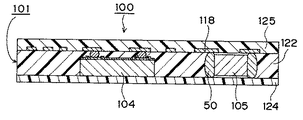
図1は、本実施形態の電子部品実装済部品製造方法を用いて製造された電子部品実装済部品を示している。尚、上記電子部品実装済部品を電子部品内蔵コアモジュール部品と記す場合もある。又、図1では、該電子部品内蔵コアモジュール部品の一例として、非接触ICカードを構成する電子部品内蔵コアモジュール部品101を示している。
上記非接触ICカードにおける電子部品内蔵コアモジュール部品101において、半導体素子104及びコンデンサ部品105は予め第1熱可塑性樹脂基材122に埋め込まれ、該第1熱可塑性樹脂基材122の、回路形成面に相当する回路パターン形成面123に露出したバンプ113及びコンデンサ部品105の電極露出面115にコイルパターン102を含む回路パターン118を形成する。回路パターン118及び電極露出面115は異方導電性ペースト等を介さずに直接に回路パターン118と導通を得る点、並びに半導体素子104及びコンデンサ部品105と、パターン形成面123との間には第1熱可塑性樹脂基材122が介在している点で従来例とは異なる。
【0017】
図2は、本実施形態の電子部品実装済部品の製造方法を用いて作製された電子部品実装済部品を備えた電子部品実装済完成品の一例としての非接触ICカード100を示している。ここで、124、125は、半導体素子104、コンデンサ部品105、及び回路パターン118を有する上記電子部品内蔵コアモジュール部品101を保護する為にラミネート処理を行なうためのシート状の部材であり、第2基材及び第3基材の機能を果たす一例である第2熱可塑性樹脂基材及び第3熱可塑性樹脂基材である。
以下に、上記電子部品実装済部品101の製造方法を含めて上記非接触ICカード100の製造方法について、図を参照して説明する。
【0018】
図10に示すステップ(図内では「S」にて示す)101において、図3に示すように、電子部品の一例に相当する半導体素子104の電極117上に、AuやCu、半田等にてなる金属ワイヤを用いたワイヤボンディング法により、バンプ113を形成する。尚、バンプ113の形成方法は、ワイヤボンディング法による形成に限定されるものではなく、めっき法による形成でも良い。又、図3に示す112は、半導体素子104のアクティブ面を保護するためのパッシベーション膜である。
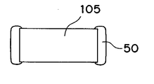
次のステップ102において、バンブ113を形成した半導体素子104、及び図4に示すように、外部電極50を有し電子部品の他の例としてのコンデンサ部品105を、ポリエチレンテレフタレート、塩化ビニル、ポリカーボネイト、アクリロニトリルブタジエンスチレン等の電気的絶縁性を有する熱可塑性樹脂で形成されたシート状の、第1基材の機能を果たす一例である第1熱可塑性樹脂基材122上にマウントする。半導体素子104及びコンデンサ部品105は、それぞれ複数個マウントする場合もあり、又、コンデンサ部品105は搭載せずに一つ若しくは複数の半導体素子104のみをマウントする場合もある。
【0019】
ここで、第1熱可塑性樹脂基材122の厚みt1は、本実施形態の場合、後述するようにバンプ113を第1熱可塑性樹脂基材122の回路パターン形成面123から露出させる必要から、基本的に半導体素子104の厚み以上で、半導体素子104の厚みとバンプ113の高さとを合わせた厚み以下にすることが望ましい。例えば、半導体素子104の厚みが0.18mm、バンプ113の高さが0.04mmの場合、第1熱可塑性樹脂基材122の厚みは0.20mmが好ましい。又、回路パターン形成面123から上記外部電極50を露出させる必要から、コンデンサ部品105は、第1熱可塑性樹脂基材122の厚みに対して50μm程度厚い厚みのものを用いることが好適である。少なくとも、厚みが第1熱可塑性樹脂基材122の厚みt1以下になること避ける必要がある。
【0020】
次のステップ103では、図6に示すように、バンプ113付の半導体素子104及びコンデンサ部品105を載置した第1熱可塑性樹脂基材122を熱プレス板171、172間に狭み、熱プレス板171、172にて、バンプ113付の半導体素子104及びコンデンサ部品105、並びに第1熱可塑性樹脂基材122を加熱しながらこれらを相対的に押圧して、図7に示すように半導体素子104及びコンデンサ部品105を第1熱可塑性樹脂基材122内に埋設する。尚、図6において、173、174は、上記押圧動作のために熱プレス板171、172を移動させる各移動装置であり、175、176は、熱プレス板171、172をそれぞれ加熱するための加熱装置である。
該熱プレス動作の条件は、例えばポリエチレンテレフタレート製の第1熱可塑性樹脂基材を用いた場合、一例として、圧力30×105Pa、温度160℃、プレス時間1分である。尚、上記温度、圧力値は、第1熱可塑性樹脂基材122の材質により異ならせる。
又、半導体素子104及びコンデンサ部品105に対する押圧動作は、それぞれ別々の熱プレス板を用いて個別に実施しても良い。
【0021】
本実施形態では、バンプ113及び電極50がそれぞれ熱プレス板171に接触した面である、バンブ113の端面115、及びコンデンサ部品105の電極50の端面51が熱プレス板171に達するまで押圧することから、図7に示すように上記プレス動作により、上記端面115及び端面51は、それぞれ第1熱可塑性樹脂基材122における上記熱プレス板171との接触面である上記回路パターン形成面123に露出することになる。
【0022】
このとき、本実施形態では薄型化を図るため、半導体素子104の上記アクティブ面に対向する裏面104a及びコンデンサ部品105の片面側105aと、上記パターン形成面123に対向する第1熱可塑性樹脂基材122の裏面122aとは、図示するように同一面となるようにしているが、これに限定されるものではない。つまり、製造する半導体部品実装済部品によっては、上述した第1熱可塑性樹脂基材122の厚みt1や、熱プレス板171、172の押圧力等の調整により、例えば、第1熱可塑性樹脂基材122の裏面122aより半導体素子104の裏面104a及びコンデンサ部品105の端面105aを突出させても良い。
【0023】
次のステップ105では、第1熱可塑性樹脂基材122における回路パターン形成面123に露出している、バンブ113の端面115、及びコンデンサ部品105の電極50の端面51と電気的接続を図るため、端面115、51に接触するようにして、Ag、Cu等の導電性ペーストを用いて回路パターン118をパターン形成面123上に形成する。尚、回路パターン118には、半導体素子104及びコンデンサ部品105と電気的に接続されるコイルパターン102を含む。該導電性ペーストによる回路パターン118の形成は、一般的にスクリーン印刷やオフセット印刷やグラビア印刷等によって行う。例えばスクリーン印刷の場合、165メッシュ/インチ、乳剤厚み10μmのマスクを介して導電性ペーストを印刷し、導体厚み約30μmの回路パターン118を形成する。
【0024】
尚、回路パターン118の形成は、導電性ペーストの印刷による形成に限定されるものではなく、Cu、Ni、アルミニウム等の金属メッキにより形成しても良い。
又、形成される回路パターン118は、本実施形態では、半導体素子104と無線にて情報の送受信を行なう為のアンテナコイルの形状である。勿論、上記回路パターン118は、上記アンテナコイル形状に限定されるものではなく、製造物としての電子部品実装済部品の機能に応じた形態に形成される。
このようにして、回路パターン118への半導体素子104及びコンデンサ部品105の実装を行ない図1に示す電子部品内蔵コアモジュール部品101が形成される。さらに以下の工程を実行することで、即ち電子部品実装済完成品の製造方法を実行することで、電子部品実装済完成品、本実施形態では非接触ICカード100が作製される。
【0025】
次のステップ106では、図8に示すように、上記電子部品内蔵コアモジュール部品101をその厚み方向からポリエチレンテレフタレート、塩化ビニル、ポリカーボネイト、アクリロニトリルブタジエンスチレン等電気的絶縁性を有するシート状の第2熱可塑性樹脂基材124及び第3熱可塑性樹脂基材125にてサンドイッチして、ラミネート処理し、電子部品内蔵コアモジュール部品101の封止を行なう。該ラミネート処理は、加熱された平面プレス板201、202により加熱、加圧して実施する。処理条件は、例えばポリエチレンテレフタレート製の熱可塑性樹脂基材を用いた場合、圧力30×105Pa、温度160℃、昇圧時間1分、圧力保持時間1分である。尚、図8において、205、206は、上記押圧動作のために平面プレス板201、202を移動させる各移動装置であり、207、208は、平面プレス板201、202をそれぞれ加熱するための加熱装置である。
【0026】
又、上記ラミネート処理は、図9に示すロールプレス方式により実施しても良い。図9において203、204は加熱されたローラーである。電子部品内蔵コアモジュール101をその厚み方向からサンドイッチする形でポリエチレンテレフタレート、塩化ビニル、ポリカーボネイト、アクリロニトリルブタジエンスチレン等電気的絶縁性を有するシート状の第2熱可塑性樹脂基材124及び第3熱可塑性樹脂基材125をローラー203、204間に供給し、ラミネート処理していく。処理条件は、例えばポリエチレンテレフタレート製の熱可塑性樹脂基材124、125を用いた場合、圧力30×105Pa、温度140℃、ラミネート速度0.1m/分である。尚、図9において、209、210は、上記押圧動作のためにローラ203、204を回転させる各駆動装置であり、211、212は、ローラ203、204をそれぞれ加熱するための加熱装置である。
以上の工程を経て、図2に示すような、半導体素子104及びコンデンサ部品105が実装されたモジュールとしての電子部品実装済部品や、本実施形態の場合のように電子部品実装済完成品としての機能を果たす一例に相当する非接触ICカード100が完成する。
【0027】
このように本実施形態によれば、第1熱可塑性樹脂基材122に半導体素子104及びコンデンサ部品105を予め埋め込んだ後に、カード化を実施する為、実装されている半導体素子104及びコンデンサ部品105と第1基材122の表面との間に段差が無い。その為、従来例における図24及び図25に示すように第2基材1bがその段差hになじまず、半導体素子4及び電子部品5周辺に気体170が残り、外観上膨れや凹み等不良が生じることは無い。
又、第1熱可塑性樹脂基材122に半導体素子104及びコンデンサ部品105を予め埋め込んだ後、半導体素子104及びコンデンサ部品105と電気的接続を図って回路パターン118を形成することから、従来例における図23に示すようなカード化後における半導体素子4の基材1aへの沈み込みは発生せず、回路パターン6が断線することは無く、高品質の電子部品実装済部品及び電子部品実装済宛成品を製造することが可能になる。
【0028】
さらに、高価な異方導電性シートまたは異方導電性粒子等の接合材料を用いる必要が無い為、加熱押圧動作を要する異方導電性シート等の処理に要する工程は必要ない。よって耐熱性の低いシート基材を使用することができ、かつ第1基材122の劣化を招くこともない。よって、高品質、高生産性旦つ安価な電子部品実装済部品及び電子部品実装済完成品を提供することが可能になる。
尚、上述した図1〜図9は半導体素子104、コンデンサ部品105と回路パターン118の接続箇所のみを示したものであり、電子部品実装済完成品の全体を示すものではない。
【0029】
第2実施形態;
上述の第1実施形態では、半導体素子104のバンプ113等が第1熱可塑性樹脂基材122のパターン形成面123に露出可能な場合を例に採ったが、例えば第1熱可塑性樹脂基材122の厚みt1よりかなり厚みの薄い半導体素子104やコンデンサ部品105を第1熱可塑性樹脂基材122に埋設する場合には、図11に示すように、埋設工程のみでは半導体素子104のバンプ113上やコンデンサ部品105の電極50上には未だ樹脂の残余部分301が存在し、上記パターン形成面123にバンプ113や電極50を露出できないときもある。
当該第2実施形態は、このような場合に対応するものである。即ち、図11に示すように、上記ステップ104の後でステップ105の前に、第1熱可塑性樹脂基材122のパターン形成面123側より、半導体素子104のバンプ113及びコンデンサ部品105の電極50上を、加熱された露出用部材300で押圧することで、図12に示すようにバンブ113及び電極50上の樹脂301を押しのけ、バンプ113及び電極50をパターン形成面123に露出させる。
【0030】
このように第2実施形態によれば、上記埋設工程のみではバンブ113及び電極50をパターン形成面123に露出できない場合でも、上記露出用部材300を用いた露出工程によりバンブ113及び電極50をパターン形成面123に露出させることができる。よってその後、上記ステップ105、さらには上記ステップ106を実行することが可能となる。
さらに又、第2実施形態によれば図13に示すように、電極117にバンブ113を形成していない半導体素子1041や、電極が突出していないフィルム状のコンデンサ部品であっても使用が可能となる。よって、種々の形態の電子部品が使用可能となり電子部品の選択範囲を拡大することができる。
上記露出用部材300の押圧条件は、例えば、200℃に加熱され、荷重980mNである。
【0031】
又、露出用部材300による上記露出工程は、バンプ113や電極50の上記パターン形成面123における露出面積をより拡大するために実行することもできる。即ち、図7に示すように、半導体素子104及びコンデンサ部品105を第1熱可塑性樹脂基材122に埋設したとき、既にバンプ113や電極50がパターン形成面123に露出している場合であっても上記露出工程を実行してもよい。該動作により、バンプ113や電極50のパターン形成面123における露出面積をより拡大することができ、導電性ペーストとの接合強度が増し、接合信頼性を向上させることができる。
【0032】
第3実施形態;
該第3実施形態では、上記ステップ105の終了後、ステップ106の実行前に、図14に示すように、図1に示す電子部品内蔵コアモジュール部品101をその厚み方向から押圧用部材302、303にて加熱、加圧する。該加熱、加圧条件は、例えば、圧力30×105Pa、温度160℃、昇圧時間1分、圧力保持時間1分である。
該押圧動作により、第1熱可塑性樹脂基材122のパターン形成面123に形成されている上記回路パターン118は、第1熱可塑性樹脂基材122内に埋め込まれる。よって、図14に示す、第1熱可塑性樹脂基材122の回路パターン形成面123と回路パターン118との、数μm〜数十μmにてなる段差h2が無くなり、図15に示すようにパターン形成面123が平坦な電子部品内蔵コアモジュール部品106が作製される。
【0033】
上記電子部品内蔵コアモジュール部品106によれば、該電子部品内蔵コアモジュール部品106を上記第2、第3の熱可塑性樹脂基材124、125で封止する際に、気体溜まり発生の原因となる段差がμmレベルのオーダーで無くなるため、上記膨れ等の外観上の不良発生が無い。よって、高品質の電子部品実装済完成品を安定して供給することができる。
【0034】
【発明の効果】
以上詳述したように本発明の第1態様における電子部品実装済部品の製造方法によれば、第1基材に電子部品を埋め込み、該第1基材上に上記電子部品と電気的に接続する回路パターンを形成したことから、従来のように異方導電性部材を用いる必要がない。よって、上記異方導電性部材を本圧着するために必要であった、例えば200℃以上の加熱動作が不要となる。したがって、上記異方導電性部材用の加熱動作は不要となり、かつ耐熱性に劣る上記第1基材について加熱が原因で劣化することはなく、かつ高価な異方導電性部材の使用を排除できるので、高品質、高生産で安価な半導体部品実装済部品の製造方法を提供することができる。
【0035】
又、上記電子部品の埋設後、該電子部品の電極を露出させた後、上記回路パターンの形成を行なうことで、例えば第1基材の厚みよりかなり厚みの薄い電子部品を第1基材に埋設した場合であっても、埋設した電子部品と上記回路パターンとを電気的に接続することができる。よって、種々の形態の電子部品が使用可能となり電子部品の選択範囲を拡大することができる。
【0036】
上記第1基材の回路形成面上に形成した上記回路パターンを当該第1基材内へ押し込み上記回路形成面を平坦化することができる。
【0037】
本発明の第2態様における電子部品実装済完成品の製造方法、及び第3態様における半導体部品実装済完成品によれば、上記第1態様の製造方法にて製造された電子部品実装済部品を使用することから、高品質、高生産で安価な電子部品実装済完成品の製造方法、及び半導体部品実装済完成品を提供することができる。
【0038】
又、電子部品を埋設することから、従来のような、第1基材と電子部品との段差は無くなる。よって、上記電子部品実装済部品を第2基材及び第3基材にてラミネート処理したとき、電子部品の周辺に気体が残り、半導体部品実装済完成品の外観上、膨れや凹み等の不良が生じることは無い。さらに、上述のように電子部品は第1基材内に埋設され、かつ上記第1基材上に回路パターンを形成したことから、ラミネート処理したとき、従来発生したような電子部品の基材への沈み込みは発生せず、回路パターンが断線することは無い。よって、高品質の電子部品実装済完成品を安定して供給することができる。
【0039】
又、上記回路形成面の平坦化により、当該電子部品実装済部品をラミネート処理して電子部品実装済完成品を作製するとき、膨れ等の外観上の不良発生を無くすことができる。よって、高品質の電子部品実装済完成品を安定して供給することができる。
【図面の簡単な説明】
【図1】 本発明の実施形態における電子部品内蔵コアモジュール部品の断面図である。
【図2】 本発明の実施形態における電子部品実装済完成品の断面図である。
【図3】 図1、図2に示す電子部品内蔵コアモジュール部品、及び電子部品実装済完成品の製造過程を説明するための図であり、半導体素子を示す図である。
【図4】 図1、図2に示す電子部品内蔵コアモジュール部品、及び電子部品実装済完成品に含まれるコンデンサ部品を示す図である。
【図5】 図1、図2に示す電子部品内蔵コアモジュール部品、及び電子部品実装済完成品の製造過程を説明するための図であり、第1熱可塑性樹脂基材上に半導体素子及びコンデンサ部品を載置した状態を示す図である。
【図6】 図1、図2に示す電子部品内蔵コアモジュール部品、及び電子部品実装済完成品の製造過程を説明するための図であり、半導体素子等を第1熱可塑性樹脂基材へ押し込む状態を示す図である。
【図7】 図1、図2に示す電子部品内蔵コアモジュール部品、及び電子部品実装済完成品の製造過程を説明するための図であり、半導体素子等を第1熱可塑性樹脂基材内に埋設した状態を示す図である。
【図8】 図1に示す電子部品内蔵コアモジュール部品を備えた電子部品実装済完成品の製造過程を説明するための図であり、電子部品内蔵コアモジュール部品を平面プレス板にてラミネート処理する状態を示す図である。
【図9】 図1に示す電子部品内蔵コアモジュール部品を備えた電子部品実装済完成品の製造過程を説明するための図であり、電子部品内蔵コアモジュール部品をローラにてラミネート処理する状態を示す図である。
【図10】 電子部品実装済完成品の製造過程を示すフローチャートである。
【図11】 本発明の第2実施形態における電子部品内蔵コアモジュール部品の製造方法における露出工程を説明するための図である。
【図12】 上記露出工程にてバンプ等が露出した状態における電子部品内蔵コアモジュール部品の断面図である。
【図13】 上記露出工程が適用可能な電子部品の一例を説明するための図である。
【図14】 本発明の第3実施形態における電子部品内蔵コアモジュール部品の製造方法を説明するための図である。
【図15】 図14に示す製造方法にて作製された電子部品内蔵コアモジュール部品の断面図である。
【図16】 従来の非接触ICカードの構造を示す斜視図である。
【図17】 従来の非接触ICカードの製造工程を示すフローチャートである。
【図18】 従来の非接触ICカードの製造工程を示す断面図である。
【図19】 従来の非接触ICカードの製造工程を示す断面図である。
【図20】 従来の非接触ICカードの製造工程を示す断面図である。
【図21】 従来の非接触ICカードの製造工程を示す断面図である。
【図22】 従来の非接触ICカードの構造を示す断面図である。
【図23】 従来の非接触ICカードの不具合状態を示す断面図である。
【図24】 従来の非接触ICカードの構造において基材と電子部品との段差を説明するための図である。
【図25】 従来の非接触ICカードの不具合状態を示す断面図である。
【符号の説明】
100…非接触ICカード、101…電子部品内蔵コアモジュール部品、
122…第1熱可塑性樹脂基材、104…半導体素子、105…電子部品、
117…電極、118…回路パターン、123…パターン形成面、
124…第2熱可塑性樹脂基材、125…第3熱可塑性樹脂基材。[0001]
BACKGROUND OF THE INVENTION
The present invention relates to an electronic component mounted component manufacturing method for manufacturing a semiconductor component mounted component by mounting an electronic component such as an IC chip on a base material, and an electronic device having an electronic component mounted component manufactured by the manufacturing method. The present invention relates to a method for manufacturing a component-mounted finished product, and a semiconductor component-mounted finished product manufactured by the electronic component-mounted finished product manufacturing method. The electronic component mounted component manufacturing method uses, for example, a conductive paste such as Ag or Cu or a plating method on a circuit pattern formed of aluminum, Cu, Ni, etc., as in the case of manufacturing a non-contact IC card. It is used when the IC chip is electrically connected to the provided connection pads.
[0002]
[Prior art]
Taking a non-contact IC card as an example, a conventional method of manufacturing an electronic component mounted finished product will be described below with reference to FIGS.
Conventionally, when manufacturing a non-contact IC card that incorporates a coil and an IC chip and transfers data to and from the outside through the coil, the coil can be formed by using a winding coil made of copper. A method of using, a method of printing and forming a conductive paste such as a silver paste, a method of forming a coil by etching a metal foil such as a copper foil, etc. are used. There are many methods for forming circuit patterns and coils.
[0003]
16 to 25 show a conventional non-contact IC card and a manufacturing method thereof.
As shown in FIG. 16, in the conventional non-contact IC card, the
In the manufacturing process, as shown in FIG. 17, first, in step (indicated by “S” in the figure) 1, a circuit pattern including a
[0004]
In
[0005]
In
In
[0006]
[Problems to be solved by the invention]
However, the conventional semiconductor component mounted finished product manufacturing method described above and the configuration of the non-contact IC card as the semiconductor component mounted finished product manufactured by the manufacturing method have the following problems.
In general, inexpensive thermoplastic resins such as polyethylene terephthalate and vinyl chloride are used for the
Moreover, in order to fix components, such as the
[0007]
Furthermore, since the
Further, as shown in FIG. 24, when the lamination process is performed in the
The present invention has been made to solve such problems, and a manufacturing method of electronic component mounted components for manufacturing semiconductor component mounted components, which is high quality, high productivity and inexpensive, and the manufacturing method. It is an object of the present invention to provide a manufacturing method of an electronic component mounted finished product having an electronic component mounted component to be manufactured, and a semiconductor component mounted finished product manufactured by the electronic component mounted finished product manufacturing method.
[0008]
[Means for Solving the Problems]
In order to achieve the above object, the present invention is configured as follows.
In the first aspect of the present invention, the electronic component mounted component manufacturing method includes a first base material made of a thermoplastic resin material and placed with a circuit pattern forming surface in contact with a hot press plate, and the circuit pattern. Relatively pressing the heated electronic component placed on the back surface of the first base material facing the forming surface,The remaining portion of the first base material is present between the electrode of the electronic component and the circuit pattern forming surface.The electronic component is embedded in the first base material,
Pushing away the remaining portion with an exposing member from the circuit pattern forming surface side to expose the electrode on the circuit pattern forming surface,
Of the above electronic componentsExposed electrodeA circuit pattern electrically connected to the circuit pattern forming surface of the first base material,electrodeAnd electrical connection between the circuit pattern and
It is characterized by that.
[0012]
In the second aspect of the present invention, the electronic component mounted finished product manufacturing method uses the electronic component mounted component manufacturing method of the first aspect to manufacture an electronic component mounted component,
After the electrical connection between the electrode and the circuit pattern, the first base material is laminated on the second base material and the third base material from the thickness direction of the first base material.
[0013]
In addition, the electronic component mounted finished product according to the third aspect of the present invention is manufactured by the electronic component mounted finished product manufacturing method according to the second aspect.
[0014]
In addition, in the completed electronic component mounted product according to the third aspect, since the non-contact IC card is configured, the circuit pattern can be formed in an antenna coil shape for transmitting and receiving information wirelessly.
[0015]
DETAILED DESCRIPTION OF THE INVENTION
An electronic component mounted component manufacturing method, an electronic component mounted finished product manufacturing method, and an electronic component mounted finished product, which are embodiments of the present invention, will be described below with reference to the drawings. Here, the manufacturing method of the electronic component mounted finished product is a method of manufacturing an electronic component mounted finished product having an electronic component mounted component manufactured by the electronic component mounted component manufacturing method, and The electronic component mounted finished product is manufactured by the electronic component mounted finished product manufacturing method. In addition, the same code | symbol is attached | subjected about the same component in each figure.
In the present embodiment, a non-contact IC card is taken as an example to fulfill the function of the above-mentioned “completed electronic component mounted product”. However, the present invention is not limited to this.
[0016]
1st Embodiment;
FIG. 1 shows an electronic component mounted component manufactured by using the electronic component mounted component manufacturing method of the present embodiment. The electronic component mounted component may be referred to as an electronic component built-in core module component. FIG. 1 shows an electronic component built-in
In the electronic component built-in
[0017]
FIG. 2 shows a
Below, the manufacturing method of the said
[0018]
In step (shown as “S” in the drawing) 101 shown in FIG. 10, as shown in FIG. 3, Au, Cu, solder, or the like is formed on the
In the
[0019]
Here, the thickness t1 of the first thermoplastic
[0020]
In the next step 103, as shown in FIG. 6, the first
For example, when the first thermoplastic resin substrate made of polyethylene terephthalate is used, the conditions for the hot press operation are as follows.5Pa, temperature 160 ° C.,
Moreover, you may implement separately the press operation with respect to the
[0021]
In the present embodiment, the
[0022]
At this time, in this embodiment, in order to reduce the thickness, the first thermoplastic resin substrate facing the
[0023]
In the
[0024]
The
In the present embodiment, the formed
In this manner, the
[0025]
In the
[0026]
The laminating process may be performed by a roll press method shown in FIG. In FIG. 9, 203 and 204 are heated rollers. A sheet-like second thermoplastic
Through the above steps, as shown in FIG. 2, an electronic component mounted component as a module on which the
[0027]
As described above, according to the present embodiment, the
In addition, since the
[0028]
Furthermore, since it is not necessary to use a bonding material such as an expensive anisotropic conductive sheet or anisotropic conductive particles, a process required for processing an anisotropic conductive sheet or the like that requires a heating and pressing operation is not necessary. Therefore, a sheet base material having low heat resistance can be used, and the
1 to 9 described above show only the connection points of the
[0029]
A second embodiment;
In the above-described first embodiment, the case where the
The second embodiment corresponds to such a case. That is, as shown in FIG. 11, after
[0030]
As described above, according to the second embodiment, even if the
Furthermore, according to the second embodiment, as shown in FIG. 13, even the
The pressing condition of the
[0031]
Further, the exposing step by the exposing
[0032]
A third embodiment;
In the third embodiment, after
The
[0033]
According to the electronic component built-in
[0034]
【The invention's effect】
As described above in detail, according to the method for manufacturing an electronic component mounted component in the first aspect of the present invention, the electronic component is embedded in the first base material and electrically connected to the electronic component on the first base material. Since the circuit pattern to be formed is formed, there is no need to use an anisotropic conductive member as in the prior art. Therefore, a heating operation of, for example, 200 ° C. or higher, which is necessary for the main pressure bonding of the anisotropic conductive member, is not necessary. Therefore, the heating operation for the anisotropic conductive member is not necessary, and the first base member having poor heat resistance is not deteriorated due to heating, and the use of an expensive anisotropic conductive member can be eliminated. Therefore, it is possible to provide a method for manufacturing a semiconductor component mounted component which is high quality, high production and inexpensive.
[0035]
Further, after embedding the electronic component, exposing the electrode of the electronic component and then forming the circuit pattern, for example, an electronic component having a thickness much thinner than the thickness of the first substrate is used as the first substrate. Even when embedded, the embedded electronic component and the circuit pattern can be electrically connected. Therefore, various types of electronic components can be used, and the selection range of electronic components can be expanded.
[0036]
The circuit pattern formed on the circuit formation surface of the first substrate can be pushed into the first substrate to flatten the circuit formation surface.
[0037]
According to the manufacturing method of the electronic component mounted finished product in the second aspect of the present invention and the semiconductor component mounted finished product in the third aspect, the electronic component mounted component manufactured by the manufacturing method of the first aspect is Since it is used, it is possible to provide a method for manufacturing an electronic component mounted finished product that is high quality, high production, and inexpensive, and a semiconductor component mounted finished product.
[0038]
Further, since the electronic component is embedded, there is no step between the first base material and the electronic component as in the prior art. Therefore, when the above-mentioned electronic component mounted component is laminated with the second base material and the third base material, gas remains around the electronic component, and the appearance of the finished semiconductor component mounted product is defective such as swelling or dent. Will not occur. Further, as described above, since the electronic component is embedded in the first base material and the circuit pattern is formed on the first base material, when the lamination process is performed, the electronic component base material as conventionally generated is obtained. No sinking occurs and the circuit pattern does not break. Therefore, it is possible to stably supply a high-quality electronic component mounted finished product.
[0039]
In addition, by flattening the circuit forming surface, it is possible to eliminate appearance defects such as swelling when the electronic component mounted component is laminated to produce a finished electronic component mounted product. Therefore, it is possible to stably supply a high-quality electronic component mounted finished product.
[Brief description of the drawings]
FIG. 1 is a cross-sectional view of an electronic component built-in core module component according to an embodiment of the present invention.
FIG. 2 is a cross-sectional view of an electronic component mounted finished product in the embodiment of the present invention.
FIG. 3 is a diagram for explaining a manufacturing process of the electronic component built-in core module component and the electronic component mounted finished product illustrated in FIGS. 1 and 2, and is a diagram illustrating a semiconductor element;
FIG. 4 is a diagram showing electronic component built-in core module components shown in FIGS. 1 and 2 and capacitor components included in the finished electronic component mounted product.
FIG. 5 is a view for explaining a manufacturing process of the electronic component built-in core module component and the electronic component mounted finished product shown in FIGS. 1 and 2; a semiconductor element and a capacitor on the first thermoplastic resin substrate; It is a figure which shows the state which mounted components.
6 is a view for explaining a manufacturing process of the electronic module with a built-in electronic component shown in FIG. 1 and FIG. 2 and a finished product mounted with an electronic component, in which a semiconductor element or the like is pushed into the first thermoplastic resin base material. It is a figure which shows a state.
FIG. 7 is a diagram for explaining a manufacturing process of the electronic component built-in core module component and the electronic component mounted finished product shown in FIGS. 1 and 2, in which a semiconductor element or the like is placed in the first thermoplastic resin substrate; It is a figure which shows the state embed | buried.
8 is a diagram for explaining a manufacturing process of an electronic component-mounted finished product including the electronic component built-in core module component shown in FIG. 1, and laminating the electronic component built-in core module component with a flat press plate; It is a figure which shows a state.
FIG. 9 is a diagram for explaining a manufacturing process of an electronic component mounted finished product including the electronic module with a built-in electronic component shown in FIG. 1, and a state in which the core module with a built-in electronic component is laminated by a roller; FIG.
FIG. 10 is a flowchart showing a manufacturing process of an electronic component mounted finished product.
FIG. 11 is a view for explaining an exposure step in the manufacturing method of the core module component with built-in electronic component in the second embodiment of the present invention.
FIG. 12 is a cross-sectional view of the electronic component built-in core module component in a state where bumps and the like are exposed in the exposing step.
FIG. 13 is a view for explaining an example of an electronic component to which the exposure process can be applied.
FIG. 14 is a view for explaining a manufacturing method of the electronic component built-in core module component according to the third embodiment of the present invention.
15 is a cross-sectional view of an electronic component built-in core module component manufactured by the manufacturing method shown in FIG. 14;
FIG. 16 is a perspective view showing the structure of a conventional non-contact IC card.
FIG. 17 is a flowchart showing a manufacturing process of a conventional non-contact IC card.
FIG. 18 is a cross-sectional view showing a manufacturing process of a conventional non-contact IC card.
FIG. 19 is a cross-sectional view showing a manufacturing process of a conventional non-contact IC card.
FIG. 20 is a cross-sectional view showing a manufacturing process of a conventional non-contact IC card.
FIG. 21 is a cross-sectional view showing a manufacturing process of a conventional non-contact IC card.
FIG. 22 is a cross-sectional view showing the structure of a conventional non-contact IC card.
FIG. 23 is a cross-sectional view showing a defect state of a conventional non-contact IC card.
FIG. 24 is a diagram for explaining a step between a base material and an electronic component in the structure of a conventional non-contact IC card.
FIG. 25 is a cross-sectional view showing a defect state of a conventional non-contact IC card.
[Explanation of symbols]
100: Non-contact IC card, 101: Core module component with built-in electronic component,
122 ... 1st thermoplastic resin base material, 104 ... Semiconductor element, 105 ... Electronic component,
117 ... Electrode, 118 ... Circuit pattern, 123 ... Pattern forming surface,
124: second thermoplastic resin base material, 125: third thermoplastic resin base material.
Claims (4)
上記回路パターン形成面側より露出用部材にて上記残余部分を押し退け上記電極を上記回路パターン形成面に露出させ、
上記電子部品の露出した電極と電気的に接続する回路パターンを、上記第1基材の回路パターン形成面に形成して上記電極と上記回路パターンとの電気的接続を図る、
ことを特徴とする電子部品実装済部品の製造方法。A first substrate made of a thermoplastic resin material and placed on the circuit pattern forming surface in contact with the hot press plate, and placed on the back surface of the first substrate facing the circuit pattern forming surface and heated. The electronic component is relatively pressed against each other so that the remaining portion of the first base material exists between the electrode of the electronic component and the circuit pattern forming surface, and the electronic component is inserted into the first base material. Buried,
Pushing away the remaining portion with an exposing member from the circuit pattern forming surface side to expose the electrode on the circuit pattern forming surface,
Forming a circuit pattern to be electrically connected to the exposed electrode of the electronic component on the circuit pattern forming surface of the first base material to achieve electrical connection between the electrode and the circuit pattern;
The manufacturing method of the electronic component mounting components characterized by the above-mentioned.
上記電極と上記回路パターンとの上記電気的接続後、上記第1基材の厚み方向から第2基材及び第3基材にて上記第1基材のラミネート処理を行なうことを特徴とする電子部品実装済完成品の製造方法。 After the electrical connection between the electrode and the circuit pattern, the first base material is laminated on the second base material and the third base material from the thickness direction of the first base material. Manufacturing method of finished product with parts mounted.
Priority Applications (1)
| Application Number | Priority Date | Filing Date | Title |
|---|---|---|---|
| JP2001061797A JP3916405B2 (en) | 2001-03-06 | 2001-03-06 | Electronic component mounted component manufacturing method, electronic component mounted finished product manufacturing method, and semiconductor component mounted finished product |
Applications Claiming Priority (1)
| Application Number | Priority Date | Filing Date | Title |
|---|---|---|---|
| JP2001061797A JP3916405B2 (en) | 2001-03-06 | 2001-03-06 | Electronic component mounted component manufacturing method, electronic component mounted finished product manufacturing method, and semiconductor component mounted finished product |
Publications (3)
| Publication Number | Publication Date |
|---|---|
| JP2002261421A JP2002261421A (en) | 2002-09-13 |
| JP2002261421A5 JP2002261421A5 (en) | 2005-05-19 |
| JP3916405B2 true JP3916405B2 (en) | 2007-05-16 |
Family
ID=18921029
Family Applications (1)
| Application Number | Title | Priority Date | Filing Date |
|---|---|---|---|
| JP2001061797A Expired - Fee Related JP3916405B2 (en) | 2001-03-06 | 2001-03-06 | Electronic component mounted component manufacturing method, electronic component mounted finished product manufacturing method, and semiconductor component mounted finished product |
Country Status (1)
| Country | Link |
|---|---|
| JP (1) | JP3916405B2 (en) |
Families Citing this family (12)
| Publication number | Priority date | Publication date | Assignee | Title |
|---|---|---|---|---|
| JP4916087B2 (en) * | 2002-12-05 | 2012-04-11 | ミッドトロニクス インコーポレイテッド | Storage battery with integrated battery tester |
| JP4228677B2 (en) | 2002-12-06 | 2009-02-25 | パナソニック株式会社 | Circuit board |
| JP4200285B2 (en) | 2003-04-02 | 2008-12-24 | パナソニック株式会社 | Circuit board manufacturing method |
| JP4602208B2 (en) * | 2004-12-15 | 2010-12-22 | 新光電気工業株式会社 | Electronic component mounting structure and manufacturing method thereof |
| US9122968B2 (en) | 2012-04-03 | 2015-09-01 | X-Card Holdings, Llc | Information carrying card comprising a cross-linked polymer composition, and method of making the same |
| WO2014159026A1 (en) * | 2013-03-14 | 2014-10-02 | X-Card Holdings, Llc | Information carrying card for displaying one time passcodes, and method of making the same |
| WO2014149926A1 (en) | 2013-03-15 | 2014-09-25 | X-Card Holdings, Llc | Methods of making a core layer for an information carrying card, and resulting products |
| KR102281468B1 (en) * | 2014-07-16 | 2021-07-27 | 삼성전기주식회사 | Chip embedded substrate and method of manufacturing the same |
| WO2018030134A1 (en) | 2016-08-12 | 2018-02-15 | 株式会社村田製作所 | Lc filter and method for producing lc filter |
| JP6658607B2 (en) | 2017-02-22 | 2020-03-04 | オムロン株式会社 | Product manufacturing method, exterior parts and antenna pattern selection device |
| CN111819577A (en) | 2018-03-07 | 2020-10-23 | X卡控股有限公司 | Metal card |
| CN112969284B (en) * | 2021-02-19 | 2022-06-24 | 深圳市众芯诺科技有限公司 | Embedded optical character intelligent recognition chip |
-
2001
- 2001-03-06 JP JP2001061797A patent/JP3916405B2/en not_active Expired - Fee Related
Also Published As
| Publication number | Publication date |
|---|---|
| JP2002261421A (en) | 2002-09-13 |
Similar Documents
| Publication | Publication Date | Title |
|---|---|---|
| US6664645B2 (en) | Method of mounting a semiconductor chip, circuit board for flip-chip connection and method of manufacturing the same, electromagnetic wave readable data carrier and method of manufacturing the same, and electronic component module for an electromagnetic wave readable data carrier | |
| US6780668B1 (en) | Package of semiconductor device and method of manufacture thereof | |
| US7229293B2 (en) | Connecting structure of circuit board and method for manufacturing the same | |
| JP4334996B2 (en) | SUBSTRATE FOR MULTILAYER WIRING BOARD, DOUBLE WIRE WIRING BOARD AND METHOD FOR PRODUCING THEM | |
| JP3916405B2 (en) | Electronic component mounted component manufacturing method, electronic component mounted finished product manufacturing method, and semiconductor component mounted finished product | |
| US7375421B2 (en) | High density multilayer circuit module | |
| US7122087B2 (en) | Method of manufacturing RFID | |
| JP2007110010A (en) | Flexible printed wiring board, flexible printed circuit board, and their manufacturing method | |
| JP3529657B2 (en) | Method of attaching semiconductor element to thermoplastic resin substrate, method of manufacturing non-contact IC card, and thermoplastic resin substrate having semiconductor element attached | |
| JP3891743B2 (en) | Manufacturing method of semiconductor component mounted component, manufacturing method of semiconductor component mounted finished product, and finished semiconductor component mounted product | |
| JP4179736B2 (en) | Manufacturing method of semiconductor element mounted component and manufacturing method of semiconductor element mounted finished product | |
| JPH11250214A (en) | Method for mounting parts, ic card and its manufacture | |
| JP3916407B2 (en) | Manufacturing method of multilayer electronic component mounted component, manufacturing method of electronic component mounted finished product, and electronic component mounted finished product | |
| JP3661482B2 (en) | Semiconductor device | |
| JP4209574B2 (en) | Manufacturing method of semiconductor component mounted parts | |
| JP3979797B2 (en) | Electronic component mounted component manufacturing method, electronic component mounted finished product manufacturing method, and semiconductor component mounted finished product | |
| JP2004514291A (en) | How to attach an integrated circuit on a silicon chip to a smart label | |
| JP4285347B2 (en) | Electronic component mounted substrate and circuit module | |
| JP3881195B2 (en) | Manufacturing method of semiconductor component mounted component, semiconductor component mounted component, manufacturing method of semiconductor component mounted finished product, and semiconductor component mounted finished product | |
| JP2008235838A (en) | Semiconductor device, manufacturing method and mounting method therefor, and ic card using the device | |
| JP2823667B2 (en) | Semiconductor element mounting method | |
| JPH1159036A (en) | Non-contact ic card and its manufacture | |
| JP2008235839A (en) | Semiconductor device, and manufacturing method therefor | |
| TWI336223B (en) | Electronic device and method of manufacturing same | |
| JP2003067708A (en) | Ic tag label manufacturing method |
Legal Events
| Date | Code | Title | Description |
|---|---|---|---|
| A521 | Written amendment |
Free format text: JAPANESE INTERMEDIATE CODE: A523 Effective date: 20040706 |
|
| A621 | Written request for application examination |
Free format text: JAPANESE INTERMEDIATE CODE: A621 Effective date: 20040706 |
|
| A131 | Notification of reasons for refusal |
Free format text: JAPANESE INTERMEDIATE CODE: A131 Effective date: 20060704 |
|
| A521 | Written amendment |
Free format text: JAPANESE INTERMEDIATE CODE: A523 Effective date: 20060828 |
|
| A131 | Notification of reasons for refusal |
Free format text: JAPANESE INTERMEDIATE CODE: A131 Effective date: 20061031 |
|
| A521 | Written amendment |
Free format text: JAPANESE INTERMEDIATE CODE: A523 Effective date: 20061213 |
|
| TRDD | Decision of grant or rejection written | ||
| A01 | Written decision to grant a patent or to grant a registration (utility model) |
Free format text: JAPANESE INTERMEDIATE CODE: A01 Effective date: 20070130 |
|
| A61 | First payment of annual fees (during grant procedure) |
Free format text: JAPANESE INTERMEDIATE CODE: A61 Effective date: 20070206 |
|
| R150 | Certificate of patent or registration of utility model |
Free format text: JAPANESE INTERMEDIATE CODE: R150 |
|
| FPAY | Renewal fee payment (event date is renewal date of database) |
Free format text: PAYMENT UNTIL: 20100216 Year of fee payment: 3 |
|
| FPAY | Renewal fee payment (event date is renewal date of database) |
Free format text: PAYMENT UNTIL: 20110216 Year of fee payment: 4 |
|
| FPAY | Renewal fee payment (event date is renewal date of database) |
Free format text: PAYMENT UNTIL: 20120216 Year of fee payment: 5 |
|
| FPAY | Renewal fee payment (event date is renewal date of database) |
Free format text: PAYMENT UNTIL: 20130216 Year of fee payment: 6 |
|
| LAPS | Cancellation because of no payment of annual fees |