JP3886397B2 - Flexible board connection method - Google Patents
Flexible board connection method Download PDFInfo
- Publication number
- JP3886397B2 JP3886397B2 JP2002065554A JP2002065554A JP3886397B2 JP 3886397 B2 JP3886397 B2 JP 3886397B2 JP 2002065554 A JP2002065554 A JP 2002065554A JP 2002065554 A JP2002065554 A JP 2002065554A JP 3886397 B2 JP3886397 B2 JP 3886397B2
- Authority
- JP
- Japan
- Prior art keywords
- flexible substrate
- circuit pattern
- terminal
- fitting hole
- electrical component
- Prior art date
- Legal status (The legal status is an assumption and is not a legal conclusion. Google has not performed a legal analysis and makes no representation as to the accuracy of the status listed.)
- Expired - Fee Related
Links
Images


Landscapes
- Multi-Conductor Connections (AREA)
- Coupling Device And Connection With Printed Circuit (AREA)
- Printing Elements For Providing Electric Connections Between Printed Circuits (AREA)
- Structure Of Printed Boards (AREA)
Description
【0001】
【発明の属する技術分野】
本発明はフレキシブル基板と電気部品の端子をはんだ付けにより接続するフレキシブル基板の接続方法に関する。
【0002】
【従来の技術】
従来可動部を有する電子機器等においては、可動部と固定部の間をフレキシブル基板により接続して、固定部と可動部の間で信号や電力等の伝達を行っている。
【0003】
また可動部となる電気部品には、複数の端子を備えたものがあり、これら端子とフレキシブル基板の回路パターンは、はんだ付けにより電気的に接続されており、電気部品の端子とフレキシブル基板の接続方法としては、例えば図5ないし図7に示す方法が従来から採用されている。
【0004】
コネクタのような電気部品aは、片面または両面に複数の端子bを有する突出部cを有している。
【0005】
またフレキシブル基板dは、フイルム状の基板eと、この基板eの一方の面に形成された導電性の回路パターンfとよりなり、フレキシブル基板dの一端側に設けられた接続部kに、電気部品aの突出部cに嵌合できる長孔状の嵌合孔gが開口されている。
【0006】
前記嵌合孔gの幅t1は、予め突出部cの幅t2より大きく、または小さく形成されていて、次のようにして電気部品aの各端子bとフレキシブル基板dの回路パターンfを接続している。
【0007】
フレキシブル基板dの端部に開口された嵌合孔gの幅t1が電気部品aの突出部cの幅t2より大きい場合は、電気部品aの突出部cにフレキシブル基板dの嵌合孔gを嵌合したら、図6に示すように嵌合孔gの一方の開口縁jを突出部cの一方の側面に当接させた状態で、電気部品aの端子bとフレキシブル基板dの回路パターンfをはんだ付けしている。
【0008】
またフレキシブル基板dの端部に開口された嵌合孔gの幅t1が電気部品aの突出部cの幅t2より小さい場合は、電気部品aの突出部cにフレキシブル基板dの嵌合孔gを嵌合すると、嵌合孔gの開口縁jが突出部cの両側面に沿って図8に示すように回路パターンf側へ折り曲げられるので、この状態で電気部品aの端子bとフレキシブル基板dの回路パターンfをはんだ付けしている。
【0009】
【発明が解決しようとする課題】
しかし図6に示すように、電気部品aの突出部cの幅t2よりフレキシブル基板dの嵌合孔gの幅t1を大きくしたものでは、電気部品aの端子bとフレキシブル基板dの回路パターンfをはんだ付けした際、はんだの一部が突出部cの側面と嵌合孔gの開口縁jとの間に生じた隙間hに流れ込んではんだブリッジを発生するため、はんだブリッジにより隣接する端子b間が短絡する等の問題がある。
【0010】
また図7に示すように、電気部品aの突出部cの幅t2よりフレキシブル基板dの嵌合孔gの幅t1を小さくしたものでは、突出部cの側面に沿って回路パターンf側へ折り曲げられた開口縁jの厚みにより端子bと回路パターンfの間に段差iが発生するため、この段差iによりはんだmが分断されてはんだ付け不良が発生するなどの問題がある。
【0011】
本発明はかかる従来の問題点を改善するためになされたもので、はんだブリッジやはんだ付け不良が発生することのないフレキシブル基板の接続方法を提供することを目的とするものである。
【0012】
【課題を解決するための手段】
前記目的を達成するため本発明のフレキシブル基板の接続方法は、フレキシブル基板に形成された回路パターンと電気部品の端子をはんだ付けにより接続するフレキシブル基板の接続方法であって、フレキシブル基板の接続部に開口した嵌合孔に接続治具を回路パターン側より挿入して、嵌合孔の開口縁を折り曲げ、次にこの状態で接続治具を端子が設けられた突出部に嵌合した後、接続治具のみを突出部より抜き出して、回路パターンを端子に圧接すると共に、次にこの状態で回路パターンと端子をはんだ付けしたものである。
【0013】
前記方法により、接続治具により嵌合孔の開口縁を折り曲げた状態で電気部品の突出部をフレキシブル基板の嵌合孔へ挿入することができるため、フレキシブル基板の接続作業が短時間で能率よく行えると共に、突出部の側面と嵌合孔の開口縁の間に隙間が生じることがないため、隙間に流れ込んだはんだによりブリッジが発生して端子間が短絡する等の従来の問題点を解消することができる上、嵌合孔の開口縁が折り曲げられても、回路パターンと端子の間に段差が生じることがないため、はんだ付け不良の発生を防止することができる。
【0014】
【発明の実施の形態】
本発明の実施の形態を図1ないし図4に示す図面を参照して詳述する。
【0015】
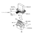
図1ないし図3は電気部品にフレキシブル基板を接続する方法を示す工程図、図4は前記接続方法により接続されたフレキシブル基板の接続構造を示す断面図である。
【0016】
フレキシブル基板1を接続する電気部品2は、図2に示すように例えばコネクタであって、外周面に二面幅が形成された筒状の本体2aの一端側に鍔部2bが突設されており、鍔部2bの端面に、段部2cを介して突出部2dが突設されている。
【0017】
突出部2dは偏平な長方体状となっていて、両側面に複数の端子3が突出部2dの長手方向に間隔を存して縦方向に形成されていると共に、突出部2dの先端には、各端子3と導通する接点3aが端子3と同数突設されている。
【0018】
またフレキシブル基板1は、フイルム状の基板1aの一方の面に導電体よりなる回路パターン1bが形成されている。
【0019】
フレキシブル基板1の一端側には、電気部品2の鍔部2bよりやや大きい長円状の接続部1cが形成されていて、この接続部1cに突出部2dの幅t2より幅t1が小さい長孔状の嵌合孔1dが開口されている。
【0020】
この嵌合孔1dの両端部には、嵌合孔1dの長辺側の開口縁1eが上下方向へ折り曲りやすいように切り欠き1fが4個所形成されていると共に、嵌合孔1dの開口縁1eには、電気部品2の各端子3と同じ配列でランド1gが形成されていて、これらランド1gは回路パターン1bの端部と電気的に導通されている。
【0021】
次に電気部品2の各端子3にフレキシブル基板1の回路パターン1bを接続する接続方法を図1ないし図3を参照して詳述する。
【0022】
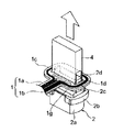
フレキシブル基板1を電気部品2の端子3に接続するに当っては、まず図1に示すような接続治具4を用意する。
【0023】
この接続治具4は、金属薄板等により偏平な箱形に形成されていて、幅t3及び横方向の長さが電気部品2の突出部2dの幅t2及び長さよりやや大きくなっており、接続治具4の一端側端面は、一端側よりほぼ中間部まで切り欠かれている。
【0024】
前記接続治具4を使用してフレキシブル基板1を電気部品2の端子3に接続するに当っては、まず図1に示すように接続治具4の一端側をフレキシブル基板1の嵌合孔1dに、回路パターン1b側から圧入する。
【0025】
接続治具4の幅t3は、予め嵌合孔1dの幅t1より大きくなっている(t1<t2<t3)ため、嵌合孔1dの開口縁1eは接続治具4によって回路パターン1bと反対の方向へ折り曲げられる。
【0026】
この状態で図2に示すように接続治具4の一端側を電気部品2の突出部2dに先端側より挿入したら、フレキシブル基板1の接続部1cが抜け出さないよう押えながら接続治具4を図3に示すように上方へ引き抜く。
【0027】
これによって嵌合孔1dの開口縁1eに形成されたランド1gが基板1aの弾性により電気部品2の各端子3に図4に示すように圧接されるので、この状態でランド1gと端子3をはんだ付けすることにより、フレキシブル基板1の回路パターン1bと電気部品2の各端子3を確実に接続することができる。
【0028】
また電気部品2の突出部2d側面とフレキシブル基板1の嵌合孔1dの間に隙間が生じることがないため、はんだブリッジが発生することがないと共に、嵌合孔1dの開口縁1eが突出部2dの側面に沿って折り曲げられても、端子3とランド1gが直接接触する方向に折り曲げられるので、はんだを分断するような段差が生じることがないため、はんだ不良が発生することもない。
【0029】
なお前記実施の形態では、突出部2dの両側に端子3が設けられた電気部品2にフレキシブル基板1を接続する場合について説明したが、突出部2dの片側に端子3を有する電気部品2にも同様に実施できるものである。
【0030】
【発明の効果】
本発明は以上詳述したように、フレキシブル基板に形成された回路パターンと電気部品の端子をはんだ付けにより接続する際、フレキシブル基板の弾性を利用して回路パターンを端子に圧接し、かつこの状態で回路パターンと端子をはんだ付けするようにしたことから、フレキシブル基板の回路パターンを電気部品の端子に直接接触させた状態で回路パターンと端子をはんだ付けできるため、フレキシブル基板と電気部品の接続が容易かつ確実に行える。
【図面の簡単な説明】
【図1】 本発明の実施の形態になるフレキシブル基板の接続方法を示す工程図
【図2】 本発明の実施の形態になるフレキシブル基板の接続方法を示す工程図
【図3】 本発明の実施の形態になるフレキシブル基板の接続方法を示す工程図
【図4】 本発明の実施の形態になるフレキシブル基板の接続構造を示す断面図
【図5】 従来のフレキシブル基板の接続方法を示す説明図
【図6】 従来のフレキシブル基板の接続構造を示す説明図
【図7】 従来のフレキシブル基板の接続構造を示す説明図
【符号の説明】
1 フレキシブル基板
1b 回路パターン
1c 接続部
1d 嵌合孔
1e 開口縁
2 電気部品
2d 突出部
3 端子
4 接続治具[0001]
BACKGROUND OF THE INVENTION
The present invention relates to how to connect the flexible substrate to be connected by soldering to terminals of the flexible substrate and the electrical component.
[0002]
[Prior art]
2. Description of the Related Art Conventionally, in an electronic device or the like having a movable part, a movable part and a fixed part are connected by a flexible substrate, and signals, electric power, etc. are transmitted between the fixed part and the movable part.
[0003]
In addition, some of the electric parts that are movable parts are equipped with a plurality of terminals. The circuit patterns of the terminals and the flexible board are electrically connected by soldering, and the terminals of the electric parts and the flexible board are connected. As a method, for example, the method shown in FIGS. 5 to 7 has been conventionally employed.
[0004]
An electrical component a such as a connector has a protrusion c having a plurality of terminals b on one side or both sides.
[0005]
The flexible substrate d is composed of a film-shaped substrate e and a conductive circuit pattern f formed on one surface of the substrate e, and an electrical connection is made to a connecting portion k provided on one end side of the flexible substrate d. A long fitting hole g that can be fitted to the protrusion c of the component a is opened.
[0006]
The width t 1 of the fitting hole g is previously formed larger or smaller than the width t 2 of the protrusion c, and the circuit pattern f of each terminal b of the electrical component a and the flexible substrate d is formed as follows. Connected.
[0007]
When the width t 1 of the fitting hole g opened at the end of the flexible substrate d is larger than the width t 2 of the protruding portion c of the electric component a, the fitting hole of the flexible substrate d is formed in the protruding portion c of the electric component a. When g is fitted, as shown in FIG. 6 , the circuit of the terminal b and the flexible substrate d of the electrical component a with one opening edge j of the fitting hole g brought into contact with one side surface of the protruding portion c. The pattern f is soldered.
[0008]
Also if the width t 1 of the apertured fitting hole g has a width t 2 is smaller than the projecting portion c of the electrical component a is the end of the flexible substrate d, mating electrical components a flexible substrate d the protrusion c of When the hole g is fitted, the opening edge j of the fitting hole g is bent toward the circuit pattern f side as shown in FIG. 8 along both side surfaces of the protrusion c, and in this state, the terminal b of the electrical component a The circuit pattern f of the flexible substrate d is soldered.
[0009]
[Problems to be solved by the invention]
However, as shown in FIG. 6 , in the case where the width t 1 of the fitting hole g of the flexible board d is larger than the width t 2 of the protrusion c of the electrical component a, the circuit of the terminal b and the flexible board d of the electrical component a When the pattern f is soldered, a part of the solder flows into the gap h formed between the side surface of the protrusion c and the opening edge j of the fitting hole g to generate a solder bridge. There is a problem such as a short circuit between the terminals b.
[0010]
Further, as shown in FIG. 7 , in the case where the width t 1 of the fitting hole g of the flexible substrate d is smaller than the width t 2 of the protrusion c of the electrical component a, the circuit pattern f side along the side surface of the protrusion c Since the step i is generated between the terminal b and the circuit pattern f due to the thickness of the opening edge j bent to the right, there is a problem that the solder m is divided by the step i to cause poor soldering.
[0011]
The present invention has been made to improve the conventional problems such, it is an object to provide a connection methods of the flexible substrate without solder bridges and soldering defects occur.
[0012]
[Means for Solving the Problems]
Method of connecting a flexible board of the present invention for achieving the above object, there is provided a method of connecting a flexible board to be connected by soldering the terminals of the circuit pattern and electrical components formed on the flexible substrate, the connecting portions of the flexible substrate Insert the connection jig into the open fitting hole from the circuit pattern side, bend the opening edge of the fitting hole, and then fit the connection jig to the protruding part with the terminal in this state, then connect jig only withdrawn from the protruding portion, the pressure contact of the circuit pattern to the terminal, it is then that the circuit pattern and the terminal was soldered in this state.
[0013]
According to the above method, since the protruding part of the electrical component can be inserted into the fitting hole of the flexible board in a state where the opening edge of the fitting hole is bent by the connecting jig, the connection work of the flexible board can be efficiently performed in a short time. In addition to being able to do this, there is no gap between the side of the protrusion and the opening edge of the fitting hole, eliminating the conventional problems such as short circuit between the terminals caused by the solder flowing into the gap. In addition, even if the opening edge of the fitting hole is bent, there is no step between the circuit pattern and the terminal, so that it is possible to prevent poor soldering.
[0014]
DETAILED DESCRIPTION OF THE INVENTION
Embodiments of the present invention will be described in detail with reference to the drawings shown in FIGS.
[0015]
1 to 3 are process diagrams showing a method of connecting a flexible substrate to an electrical component, and FIG. 4 is a cross-sectional view showing a connection structure of the flexible substrate connected by the connection method.
[0016]
As shown in FIG. 2, the
[0017]
The projecting
[0018]
In the flexible substrate 1, a
[0019]
One end side of the flexible substrate 1, have slightly larger oval-shaped connecting portion 1c from the
[0020]
At both ends of the
[0021]
Next, a connection method for connecting the
[0022]
In connecting the flexible substrate 1 to the
[0023]
The connecting jig 4 is formed in a flat box shape by a thin metal plate or the like, and the width t 3 and the lateral length are slightly larger than the width t 2 and the length of the
[0024]
In connecting the flexible substrate 1 to the
[0025]
Since the width t 3 of the connecting jig 4 is larger than the width t 1 of the
[0026]
In this state, as shown in FIG. 2, when one end side of the connection jig 4 is inserted into the protruding
[0027]
As a result, the
[0028]
Further, since no gap is generated between the side surface of the protruding
[0029]
In the above embodiment, the case where the flexible substrate 1 is connected to the
[0030]
【The invention's effect】
As described above in detail, when the circuit pattern formed on the flexible substrate and the terminal of the electrical component are connected by soldering, the present invention presses the circuit pattern against the terminal using the elasticity of the flexible substrate, and this state Since the circuit pattern and the terminal are soldered in
[Brief description of the drawings]
FIG. 1 is a process diagram showing a flexible substrate connection method according to an embodiment of the present invention. FIG. 2 is a process diagram showing a flexible substrate connection method according to an embodiment of the present invention. FIG. 4 is a sectional view showing a flexible substrate connection structure according to an embodiment of the present invention. FIG. 5 is an explanatory diagram showing a conventional flexible substrate connection method. 6 is an explanatory diagram showing a conventional flexible substrate connection structure. FIG. 7 is an explanatory diagram showing a conventional flexible substrate connection structure.
DESCRIPTION OF SYMBOLS 1
Claims (1)
Priority Applications (1)
| Application Number | Priority Date | Filing Date | Title |
|---|---|---|---|
| JP2002065554A JP3886397B2 (en) | 2002-03-11 | 2002-03-11 | Flexible board connection method |
Applications Claiming Priority (1)
| Application Number | Priority Date | Filing Date | Title |
|---|---|---|---|
| JP2002065554A JP3886397B2 (en) | 2002-03-11 | 2002-03-11 | Flexible board connection method |
Publications (2)
| Publication Number | Publication Date |
|---|---|
| JP2003264021A JP2003264021A (en) | 2003-09-19 |
| JP3886397B2 true JP3886397B2 (en) | 2007-02-28 |
Family
ID=29197805
Family Applications (1)
| Application Number | Title | Priority Date | Filing Date |
|---|---|---|---|
| JP2002065554A Expired - Fee Related JP3886397B2 (en) | 2002-03-11 | 2002-03-11 | Flexible board connection method |
Country Status (1)
| Country | Link |
|---|---|
| JP (1) | JP3886397B2 (en) |
Families Citing this family (1)
| Publication number | Priority date | Publication date | Assignee | Title |
|---|---|---|---|---|
| WO2011033632A1 (en) * | 2009-09-16 | 2011-03-24 | Kanazawa Kyohei | Waterproof connector, waterproof connection adapter, and waterproof connection structure |
-
2002
- 2002-03-11 JP JP2002065554A patent/JP3886397B2/en not_active Expired - Fee Related
Also Published As
| Publication number | Publication date |
|---|---|
| JP2003264021A (en) | 2003-09-19 |
Similar Documents
| Publication | Publication Date | Title |
|---|---|---|
| US5462443A (en) | Plug-type connector | |
| KR101683386B1 (en) | Dual thickness double-ended male blade terminal | |
| JP2949441B2 (en) | Terminal connection device | |
| JP2000077120A (en) | Terminal structure of connector | |
| JP3886397B2 (en) | Flexible board connection method | |
| JP2004134156A (en) | Electrical connector | |
| JP4358269B2 (en) | Electronic component module | |
| JP4064091B2 (en) | Manufacturing method of electrical connector | |
| US6116948A (en) | Electrical connector for terminating discrete electrical wires | |
| JP2008293892A (en) | Contact, and connector using the same | |
| JPH0818188A (en) | Connectorless printed board connection mechanism | |
| JP2005183298A (en) | Terminal fitting, terminal material, and manufacturing method of terminal fitting | |
| KR101927335B1 (en) | Connector | |
| JP3998209B2 (en) | connector | |
| JPH08315881A (en) | Surface mount connector | |
| JP2004071231A (en) | Connector for high-speed transmission | |
| JPH09116246A (en) | Connection structure of printed wiring board | |
| JP3721310B2 (en) | Connecting device for connecting two boards | |
| JPS598374Y2 (en) | printed board | |
| JPH09199242A (en) | Printed wiring board integral type connector and manufacture thereof | |
| JPH10189105A (en) | Electric connector | |
| JPH0419969A (en) | Flexible electric connector | |
| KR100647226B1 (en) | Connector pin for printed circuit board | |
| JPH09172238A (en) | Connecting terminal of circuit board | |
| JPH069079U (en) | Connector for PCB connection |
Legal Events
| Date | Code | Title | Description |
|---|---|---|---|
| A621 | Written request for application examination |
Free format text: JAPANESE INTERMEDIATE CODE: A621 Effective date: 20050304 |
|
| A977 | Report on retrieval |
Free format text: JAPANESE INTERMEDIATE CODE: A971007 Effective date: 20060227 |
|
| A131 | Notification of reasons for refusal |
Free format text: JAPANESE INTERMEDIATE CODE: A131 Effective date: 20060808 |
|
| A521 | Written amendment |
Free format text: JAPANESE INTERMEDIATE CODE: A523 Effective date: 20061004 |
|
| TRDD | Decision of grant or rejection written | ||
| A01 | Written decision to grant a patent or to grant a registration (utility model) |
Free format text: JAPANESE INTERMEDIATE CODE: A01 Effective date: 20061121 |
|
| A61 | First payment of annual fees (during grant procedure) |
Free format text: JAPANESE INTERMEDIATE CODE: A61 Effective date: 20061121 |
|
| R150 | Certificate of patent or registration of utility model |
Free format text: JAPANESE INTERMEDIATE CODE: R150 |
|
| FPAY | Renewal fee payment (event date is renewal date of database) |
Free format text: PAYMENT UNTIL: 20101201 Year of fee payment: 4 |
|
| FPAY | Renewal fee payment (event date is renewal date of database) |
Free format text: PAYMENT UNTIL: 20111201 Year of fee payment: 5 |
|
| FPAY | Renewal fee payment (event date is renewal date of database) |
Free format text: PAYMENT UNTIL: 20121201 Year of fee payment: 6 |
|
| FPAY | Renewal fee payment (event date is renewal date of database) |
Free format text: PAYMENT UNTIL: 20131201 Year of fee payment: 7 |
|
| R250 | Receipt of annual fees |
Free format text: JAPANESE INTERMEDIATE CODE: R250 |
|
| LAPS | Cancellation because of no payment of annual fees |