JP3886079B2 - Ring oscillator using delay interpolating mixer cell - Google Patents
Ring oscillator using delay interpolating mixer cell Download PDFInfo
- Publication number
- JP3886079B2 JP3886079B2 JP11479598A JP11479598A JP3886079B2 JP 3886079 B2 JP3886079 B2 JP 3886079B2 JP 11479598 A JP11479598 A JP 11479598A JP 11479598 A JP11479598 A JP 11479598A JP 3886079 B2 JP3886079 B2 JP 3886079B2
- Authority
- JP
- Japan
- Prior art keywords
- output
- delay
- mixer
- input
- stage
- Prior art date
- Legal status (The legal status is an assumption and is not a legal conclusion. Google has not performed a legal analysis and makes no representation as to the accuracy of the status listed.)
- Expired - Fee Related
Links
Images


Classifications
-
- H—ELECTRICITY
- H03—ELECTRONIC CIRCUITRY
- H03K—PULSE TECHNIQUE
- H03K3/00—Circuits for generating electric pulses; Monostable, bistable or multistable circuits
- H03K3/02—Generators characterised by the type of circuit or by the means used for producing pulses
- H03K3/023—Generators characterised by the type of circuit or by the means used for producing pulses by the use of differential amplifiers or comparators, with internal or external positive feedback
- H03K3/0231—Astable circuits
Description
【0001】
【産業上の利用分野】
本発明は、モノリシック集積型発振器に関する。より詳細には、本発明は、正確な多相出力を提供する同調可能なリング発振器に関する。
【0002】
【従来の技術】
リング発振器は、通信システムにおいて広く使用されてきた。図1は、従来のリング発振器10を示す。この発振器は、ループ内において全体として反転するように接続された、それぞれゲート遅延TDを有するN個のセル12からなる。立上り論理遷移がリングに沿って伝播すると、1周した後に立下りエッジになる。2周した後は再び立上りエッジになる。ループ内の伝播時間がN×TDなので、生成される信号の周期は2×N×TDになる。同様に、この回路は周波数、1/(2×N×TD)で発振する。TDを調整しそれにより同調可能な発振器を作成するために、様々な方法が利用されてきた。
【0003】
図1のリング発振器10からは、連結されたそれぞれのセル12から出力される合計N個の個別の出力を得ることができる。各出力の真出力と相補出力とが両方とも得られる場合は、2×N個の異なる出力クロック位相を得ることができる。これらの位相のずれた各クロック間の時間遅延は、1つのゲート遅延TDと等しい。
【0004】
多くの用途において、簡単な発振器の2×N個の位相よりも多い遅延小区分を有することが望ましい場合がある。たとえば、周波数が2.5GHZの発振器を100ピコ秒のゲート遅延TDを有するシステムで使用する場合、発振器には、周波数が1/(2×2×100ピコ秒)=2.5GHzとなるような2つのゲートがなければならない。そのような2つのセル発振器は4つの出力位相を有することになる。この発振器の用途に、たとえば8相などの5つ以上の等間隔の位相が必要な場合は、補間を提供するなんらかの方法が必要である。
【0005】
「1994 ISSCC Digest of Technical Papers」のページ58-9のT. Knottsその他による論文「A 500 MHz Time Digitizer IC with 15.625ps Resolution」には、ミクサ(混合器)を使ってこのような補間した位相を駆動する回路が開示されている。ミクサの入力は、遅延補償バッファ24として働くように相互接続される。図2aは、補間器26を使って追加の位相を生成するリング発振器20を示し、この補間器26は、リング接続されたセル22によって生成されたエッジ間を補間するために使用される。
【0006】
図2bは、N=2の特別な事例の補間発振器27を示す。中間位相(出力1,2)は、0度と90度の出力(出力1と出力2)の電圧間で平均をとることにより生成される。理想的な正弦波発振信号では、この電圧は45度において得られる。第2の平均化回路は、90度と180度の出力(出力2と出力1)の間で補間を行い、出力2,1に135度で得られる電圧を生じる。
【0007】
実際の補間回路はすべて固有のゲート遅延をもつため、位相の精度を維持するために、0度と90度の出力に遅延補償ダミー補間器24が使用される。それぞれの補間器26の出力の真と相補両方の形を取ることにより、得られる位相の数が二倍になる。この技術は、それぞれの段が利用できる位相を2倍にする複数ランクの補間器26によって任意に拡張することができる。
【0008】
外部補間器の手法にはいくつかの欠点がある。幅が広い間隔で補間すると、補間器出力における立上り時間(dv)/(dt)が遅くなり、そのため次段のジッタが大きくなる。さらに、ダミー補間器24の遅延と実際の補間器26の遅延とを一致させるのが難しい。これにより、わずかな系統的なタイミング誤差が生じる。
【0009】
R. Walkerによる米国特許第4,884,041号「Fully Integrated High-Speed Voltage Controlled Ring Oscillator」には、完全に統合され、周波数同調可能で、信号と同調電圧の両方において完全差動であるという利点を有するリング発振器が開示されている。回路内の差動入力信号と差動出力信号の2本の線によって、オンチップ電源の雑音とクロストークが抑制される。各真の信号と相補信号とは個々に同様な雑音とクロストーク・パターンとを含むため、開示されたリング発振器は、これらの真の信号と相補信号との間の差動信号対を使用して雑音を抑制する。
【0010】
Walkerの開示したリング発振器の周波数同調は、各発振器段の遅延を電子的に変化させることにより達成される。図3は、Walkerの開示したリング発振器において遅延セルとしてそれぞれ使用できる電子的に可変な遅延セル30の概略図である。この可変遅延セル30は、遅延補間ミクサ34に接続された遅延セル32に基づく。遅延補間ミクサ34は、第1の入力36と、遅延セル32によって遅延された第2の入力38との重み付き合計を実行する。アナログ同調入力37は遅延補間ミクサ34の遅延を変えるよう調節することができ、その結果、遅延が遅延補間ミクサ34自体の遅延から遅延補間ミクサ34と遅延セル32との遅延を合計した遅延までの範囲になるようにすることができる。さらに、遅延補間ミクサ34の詳細を以下に検討する。
【0011】
「1996 ISSCC Digest of Technical Papers」、pp 392〜393のRofougaranその他による論文「A 900MHZ CMOS LC-Oscillator with Quadrature Outputs」には、インタリーブ式差動発振器が開示されており、ここで周波数は、統合インダクタLとFETドレイン接合容量Cとによって設定されるが、発振器を同調することはできない。
【0012】
「IEEE Journal of Solid-State Circuits」Vol.28、No.12、1993年12月、pp. 1273〜1282のManeatisその他の論文「Precise Delay Generation Using Couple Oscillators」には、同調することはできるがシングルエンド型のインタリーブ式発振器が開示されている。同調は、電流スタービングCMOS技術を利用して行われる。
完全差動相互接続手法の利点を有しかつ周波数同調が可能で位相差が小さい発振器の設計があると有利である。
【0013】
【発明が解決しようとする課題】
本発明は、周波数同調が可能で、補間をしなくてもより多くの出力位相を発生することのできる発振器を提供することを目的とする。
【0014】
【課題を解決するための手段】
本発明によれば、追加の段を利用して外部の補間器に依存せずにより多くの出力位相を生成するリング発振器が開示される。このリング発振器は、本質的に対称であり、補間器手法の系統的な時間誤差の影響を受けない。発振器段は、発振周波数が従来の制限、1/(2×N×TD)よりも高くなるように相互接続される。
【0015】
改良したリング発振器は、発振器段の間の所定の時間間隔が、個々の段の遅延よりも短くなるように交互に配置された段を含む。発振器周波数はやはり調整可能であり、段の時間間隔は、同調範囲全体にわたり一定のままである。これにより、エッジ間隔TEを、補間器を利用せずに実現可能なゲート遅延TDよりも短くすることができる。
【0016】
【実施例】
従来のリング発振器では、各段が次の段と直列に接続される。インタリーブ式のリング発振器では、それぞれの段が複数の入力を有し、その入力は、他の複数の段の出力と接続される。段をインタリーブ式構造で相互接続することによって、以下に説明するように、従来の発振器の2×N個の位相よりも多い遅延小区分を達成することができる。
【0017】
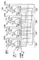
図4aは、インタリーブ式リング発振器40の簡略化した回路図を示す。図4bは、図4aに示した遅延補間ミクサ・セル42間の対称的相互接続の概略的な信号流れ図を示す。4つの段A−Dはそれぞれ、図3に示した遅延補間ミクサ34と類似の単純な遅延補間ミクサである。インタリーブ式リング発振器40の各段46は、2つの入力136および138と1つの出力39を有する遅延補間ミクサ・セル42を含む。
【0018】
図4aと図4bに示したように、遅延補間ミクサ・セル42はそれぞれ他の2つの遅延補間ミクサ・セル42に接続され、それぞれの遅延補間ミクサ・セル42の2つの入力が、2つの他のセルの出力と接続され、それぞれの遅延補間ミクサ・セル42の出力が、他の2つの遅延補間ミクサ・セル42の入力を駆動する。各セル42の一方の入力138は、すぐ左側の段46の出力39と接続される。セル42の他方の入力136は、対向するセル42の出力と接続される。たとえば、段Cの第1の入力136は、段Aの出力39に接続され、段Cの第2の入力138は段Bの出力39に接続され、段Cの出力39は段Aの入力136と段Dの入力138に接続される。段Aの入力136は、段Cの出力39からの入力信号を反転することに注意されたい。
【0019】
各ミクサ・セル42a〜42dにおいて、2つの入力136と138は、所定の重み付けで結合される。各段A〜Dの出力39は、段の各入力からの寄与を含む。好ましい実施例において、それぞれのミクサ・セルの2つの入力136と138は、等しい重み付けで結合され、したがって段の出力は、2つの入力の平均になる。
【0020】
その結果、4段インタリーブ式リング発振器40は、従来の限界、1/(2×N×TD)よりも高い1.5/(8×TD)の周波数で発振することができる。以下に、発振周波数を、4つの段A〜Dがインタリーブ式リング発振器40と同様に相互接続された同調可能なインタリーブ式リング発振器90(図5)の1つの同調状態(式1)に関して説明する。
【0021】
また、インタリーブ式リング発振器40は、外部補間器に依存せずに多くの出力位相を生成する。出力39が同一の段A〜Dによって生成されるため、出力が均一な間隔の位相を有するように補間器26とダミー補間器24(図2a、2b)の遅延を一致させる必要がない。図4aと図4bに示したインタリーブ式リング発振器40は同調可能ではないが、外部補間器で起こるような位相間隔の問題はない。
【0022】
図4aの4セル・リング発振器40を考察する1つの方法は、図4bに示したように直角位相で作動する交差結合された一対の「2リング」発振器としてである。セルAとCが0度と180度の位相で作動し、セルBとDは90度と270度の位相で作動する。さらに、セルBをCに、CをDに、DをAに、AをBにそれぞれ対称的に交差結合することによって、2つの「2段」リング発振器が構成される。2つの「2段」リング発振器は、互いにロックされたままであり、すなわち「インタリーブ」される。
【0023】
図4aおよび4bは、4つのミクサ・セル42を相互接合する好ましい方法を示す。これらの図において、「A」のミクサ・セル42aは、ミクサ・セルDおよびCによって駆動されるように示される。しかしながら、多数のミクサ・セル42を相互接続してリング発振器40を構成することができる方法はいくつかある。たとえば、ミクサ・セルAは、ミクサ・セルBとCでもミクサ・セルBとDでも駆動することができる。しかしながら、以下に検討するようなミクサ・セル42を相互接続するいくつかの方法が、他の方法よりも好ましい。
【0024】
図5は、表1の第1列に示したような4段の同調可能なインタリーブ式リング発振器90の好ましい実施例を示す。各段146は、出力139aを有する2重ミクサ・セル72を含む。また、2重ミクサ・セル72の出力は、遅延セル74に接続される。遅延セル74は、遅延セル74の遅延によって出力139aに対して遅延される第2の出力139bを生成する。各2重ミクサ・セル72は、4つの入力X、Y、XDおよびYDを有する。また、各2重ミクサ・セル72は、同調入力73を有する。4つの2重ミクサ・セル72の同調入力73は、発振器同調入力76に接続される。後で説明するように、発振器同調入力76によって、同調可能なインタリーブ式リング発振器90の動作周波数が調節される。4段の同調可能なインタリーブ式リング発振器90の各段において、遅延セル74の前と後で出力信号139aと139bが取られ、出力信号A、B、CおよびDと、遅延出力信号AD、BD、CDおよびDDを提供する。
【0025】
インタリーブ式リング発振器90の実施例において、図5(ならびに、後で検討する図8)に示したシングルエンド型の入力と出力がそれぞれ、2導体差動接続として実施される。しかしながら、図を簡素化するために1つのシングルエンド型接続だけを示す。
【0026】
好ましい4段の同調可能なインタリーブ式リング発振器90の段A、B、CおよびDは、各段の非遅延入力XおよびYが図4bに示した他の2つの段の非遅延出力139aに接続され、各段の遅延入力XDおよびYDが図4bに示した他の2つの段の遅延出力139bに接続されるように相互接続される。たとえば、段Aの入力X、XD、YおよびYDは、段Cの出力CおよびCDと、段Dの出力DおよびDDにそれぞれ接続される。同様に、段Bへの入力は、段Dの出力DおよびDDと、段AのAおよびADに接続され、段Cの入力は、段Aの出力AおよびADと、段Bの出力BおよびBDに接続され、段Dの入力は、段Bの出力BおよびBDと、段Cの出力CおよびCDに接続される。
【0027】
4段のインタリーブ式リング発振器では、表1に示したように、2重ミクサ・セル72を相互接続する異なる3つの方法がある。この表は、また、セル遅延TDに関して、それぞれの4段インタリーブ式リング発振器ごとに生じた位相遅延TEを示す。後で検討するように、2重ミクサ・セル72間の相互接続のいくつかの方法は、他の方法よりも好ましい。入力の反転に関して後で説明するように、プライム記号’は、反転入力を示すために使用される。たとえば、表1の第1列において、C’は、段Aへの入力として段Cの出力信号の反転が使用されていることを示す。
【0028】
【表1】

図6に、4段同調可能インタリーブ式リング発振器90に使用される2重入力ミクサ72の好ましい構成を示す。2重入力ミクサ72は、図3に示した遅延補間ミクサ・セル34に基づく。図6に示した回路が理解しやすいように、最初に、図3に示した補間ミクサ・セル34の周波数同調を詳しく説明する。
【0030】
図3において、アナログ同調入力37が、左側の差動トランジスタ対33aと右側の差動トランジスタ対33bとの間で相対電流を調節する。同調範囲の一方の端で、左側のトランジスタ対33aが完全に導通しており、右側のトランジスタ対33bはほとんど導通しておらず、その結果、電流源35からのほとんどすべての電流が、遅延補間ミクサ34の左側半分33aを通る。その結果、入力電圧36に応じて共通コレクタ抵抗31の両端に出力電圧が生じる。この結果、ミクサの遅延は、遅延補間ミクサ34自体の遅延と等しくなる。同調範囲の他方の端では、左側のトランジスタ対33aがほとんど導通しておらず、右側のトランジスタ対33bが完全に導通しており、電流源35からのほとんどすべての電流が遅延補間ミクサ34の右側半分33bを流れる。したがって、遅延セル32によって遅延された入力電圧に応じて、コレクタ抵抗31の両端に出力電圧が生じる。その結果、ミクサの遅延が、遅延補間ミクサ34と遅延セル32の両方の遅延の合計と等しくなる。同調範囲の他の部分では、トランジスタ対33aと33bが両方とも導通しているとき、入力電圧36と遅延セル32により遅延された入力電圧の重み付き合計に応じて、コレクタ抵抗31の両端に出力電圧が生じる。重み付けは、同調電圧37に依存する。
【0031】
図6に示した2重入力ミクサ72は、4つの差動入力対82を結合し、2重入力ミクサ72の右側半分73bと左側半分73aを含む2つの相互接続された遅延補間ミクサ34と見なすことができる。遅延補間ミクサ34は両方とも、共通コレクタ抵抗81に給電して出力電圧139を生成する。2重入力ミクサ72はそれぞれ、1つの同調入力84、X、XD、Y、YDと名付けられた4つの差動入力82、Zと名付けた差動出力139aを有する。電流源79aと79bは、2重入力ミクサ72の左側半分73aと右側半分73bにそれぞれ接続される。後で説明するように、コレクタ抵抗81を流れる全電流が、電流源79aと79bに等分される。インタリーブ式リング発振器内で実施されるとき、隣の段146からの出力139aの1つとその遅延出力139bが、差動入力82XおよびXDにそれぞれ接続され、もう1つの隣の段146からの第2の出力139aとその遅延出力139bが、差動入力82YとYDにそれぞれ接続される。
【0032】
2重入力ミクサ72の左側半分73aおよび右側半分73bと、電流源79aおよび79bを介して等しい電流i1およびi2が流されるため、出力139a Zにおいて、XとYの相対的な寄与とXDとYDの相対的な寄与とは等しく重み付けされたままである。したがって、各段146に入る2つ非遅延入力対139aは、2重入力ミクサ72によって等しく重み付けされて平均化される。また、2つの遅延入力対139bは、2重入力ミクサ72によって等しく重み付けされて平均化される。代替として、電流i1とi2の比率を1以外の値に設定することによって、入力対を等しくならないように重み付けすることもできる。
【0033】
好ましい実施例において、入力対XとXDの重みの合計は0.5であり、これは入力対YとYDにも同じことが当てはまる。したがって、「X」の出力に対する寄与と「Y」の出力に対する情報寄与は、50:50の比率で一定に維持される。たとえば、図5において、段Aに関して、段CおよびDからの入力信号は、段Aの入力XDとYDに接続された信号CDとDDだけでなく、段Aの入力XとYに接続された信号CとDを利用して平均化される。段146の出力と入力は、一定量だけ完全に結合されたままである。したがって、4つの段146は、同調範囲全体に渡って均一に結合され、その結果完全な差動同調システムが得られる。
【0034】
図6の2重入力ミクサ72を再び参照すると、同調入力84αを1〜−1の間で調整するとき、2重入力ミクサ72の出力Zの入力対XとY、およびXDとYDに与えられる相対重み付けが変化する。同調入力84αを1〜−1の間で変化させることにより、ミクサ・セル72の左側半分73aが入力XとXDの比率を変化させ、右側半分73bが入力YとYDの比率を変化させる。
【0035】
α=−1のとき、Zは、ほぼXDとYDだけであり、本質的にXとYの寄与はない。α=1のとき、ZはほぼXとYだけであり、本質的にXDとYDの寄与はない。2重入力ミクサ72の周波数は、それぞれの2重入力ミクサ72の遅延が最大となる周波数fminから、それぞれの2重入力ミクサ72の遅延が最小となる周波数fmaxまで連続的に同調可能である。同調範囲の他の部分では、2重入力ミクサ72の周波数はfminとfmaxの間にある。周波数は、非遅延入力XおよびYと遅延入力XDおよびYDの各段146の出力への相対的な寄与に依存する。同調入力84αが1のとき、駆動トランジスタQ9およびQ11には、i1とi2に等しい電流が流れる。その結果、トランジスタ対Q1とQ2およびQ5とQ6は完全に導通し、トランジスタ対Q3とQ4およびQ7とQ8はほとんど導通しなくなる。この場合、出力Zは、入力XおよびYからのみ等しく導出される。ミクサ遅延をTDMで示し、図5と表1の好ましい4段発振器90の位相遅延TEがTDM/1.5であることを起想すると、発振周波数は次の式で与えられる。
【0036】
f=(1.5/8)×(1/TDM) (1)
【0037】
これは、最大動作周波数fmaxである。
【0038】
同調入力84αが−1のとき、駆動トランジスタQ10とQ12には、ほぼi1とi2に等しい電流が流れる。この結果、トランジスタ対Q1とQ2およびQ5とQ6はほとんど導通せず、トランジスタ対Q3とQ4およびQ7とQ8が完全に導通する。この場合、出力Zは、入力XDとYDからのみ等しく導出される。
【0039】
fmin=(1.5/8)×(1/(TDM+TDC)) (2)
【0040】
これにより、最も低い周波数で発振するインタリーブ式発振器が実現され、ここでTDCは、遅延セル74の遅延である。
【0041】
図6において、2重入力ミクサ72は、まず、XとXDの間とYとYDの間で可変重み付き(すなわち同調)合計し、次に(X+XD)と(Y+YD)の間で固定重み付き合計する。代替として、図6に示した回路を、XとYの間の固定重み付き合計とXDとYDの間の固定重み付き合計を等しく行った後で、(X+XD)と(Y+YD)の間の可変重み付き(すなわち同調)合計を行うように構成することもできる。
【0042】
以上検討したように、インタリーブ式リング発振器の複数の段146を相互接続するトポロジーと呼ばれる方法は多数ある。たとえば、4段インタリーブ式リング発振器では、表1に示したように、2重入力ミクサ・セル72を相互接続する方法が3つある。
【0043】
好ましい相互接続のトポロジーは、高調波を生成するために必要な位相が、発振器が基本周波数で発振するのに必要な位相よりも2〜3倍高くなるようなものである。この条件が満たされるとき、インタリーブ式リング発振器を構成する段146の周波数ロールオフにより、次の高調波の周波数において、高調波周波数での発振を支援できないほど大きな利得の損失が起こる。これにより、基本周波数で動作が安定する。図5に示した好ましい4段インタリーブ式リング発振器90は、シミュレ−ションと測定の両方により、安定していることが示された。
【0044】
最も低いスプリアス周波数モードは、基本モードの2倍の周波数である。この周波数はほぼ段146の利得帯域幅曲線により低下する。4セルインタリーブ式発振器では、他の2つのトポロジー(表1の2列と3列)が可能である。たとえば、出力Aを、入力B’とC’あるいは入力BとD’から導出することができる。このような接続は、それぞれ、TE=TD/2.5とTE=TD/4の位相遅延を生じる。しかしながら、これらのトポロジーで段を相互接続すると、リング発振器が基本周波数以外の周波数で発振することを可能にする。そのような望ましくないモードを有する発振器の可能性は、表1において「やや有り得る」または「有り得る」として示される。この場合、段が表で示されたように相互接続されたとき、発振器は、増幅器の利得プロファイル内に生ずるスプリアス・モードの発振を有する。シミュレ−ションにおいて、これらの代替トポロジーは、リング発振器を同調するときの様々なモード間のホッピングを示す。利得プロファイル内に生ずるスプリアス・モードの発振を有するいくつかのインタリーブ式リング発振器の実施例では、発振器を、所望の周波数で確実に発振するよう既知の状態に事前設定しなければならない。
【0045】
図7は、図5の好ましいリング発振器90のために4つの段A、B、CおよびD146によって生成された4つの出力波形102a〜102dの位相の関係を示すグラフ100である。段Cの出力102cは、段Aの出力102aと段Bの出力102bとの重み付き合計から導出される。段Aの出力と段Bの出力との間の時間間隔(TE)は、段の遅延TDの1/1.5である。これは、段Cへの有効入力エッジ106が、段Aの出力と段Bの出力(104aおよび104b)とにおいてエッジが発生する時間の中間の時間で生じることを知ることにより理解することができる。そのとき、有効入力エッジ106の後の段Cのゲート遅延TDに等しい時間において、段Cの出力102cの状態が変化する。段Cの2重入力ミクサ・セル72は、段Aと段Bの出力を同じ重み付けで平均化し、それにより遷移104aおよび104bは有効エッジ106になる。その結果、段Cの出力102cにおけるエッジの中間点104cは、段Cのゲート遅延TDの後に生じる。
【0046】
類似の方法で、段Cの出力の半分と段Bの出力の半分を利用して段Dの入力を生成する。段Aの入力を生成するときは、段Cの出力の反転C’と段Dの出力のD’が使用される。段Bの入力を生成するときは、段Aの出力と段Dの出力のD’が使用される。
【0047】
全部で3つ以上の段を含む本発明のすべての実施例において、それぞれの段は、前の2つの段によって対称的に駆動される。
【0048】
図8は、3つの段146を有するシングルエンド型の周波数同調可能なインタリーブ式発振器70の概略図であり、それぞれの段146は、2つの他のミクサ・セルの出力によって駆動される2重入力ミクサ・セル72(図6)と、遅延セル74と、出力139aと、遅延出力139bとを含む。段Aへの入力は、段BとCからの出力によって駆動され、段Bへの入力は、段CとAからの出力によって駆動され、段Cへの入力は段AとBからの出力によって駆動される。以上のように、同調信号76は、インタリーブ式リング発振器70の動作周波数を調節するために使用される。
【0049】
本明細書において、本発明を好ましい実施例に関して説明したが、当業者は、本発明の範囲から逸脱することなくここで説明した応用例の代わりに他の応用例を実施できることを容易に理解されよう。
【0050】
以上、本発明の実施例について詳述したが、以下、本発明の各実施態様の例を示す。
【0051】
[実施態様1]
第1の一対の入力、第2の一対の入力、第1の出力、および前記第1の出力に対して遅延された第2の出力をそれぞれが有する少なくとも3つの混合器セルを備え、
前記混合器セルはそれぞれ前記混合器セルの他の2つに対称的に接続され、
前記混合器セルのそれぞれの前記第1の一対の入力は、前記混合器セルの前記他の2つの前記第1の出力に対称的に接続され、
前記混合器セルのそれぞれの前記第2の一対の入力は、前記混合器セルの前記他の2つの前記第2の遅延出力に対称的に接続されている、
ことを特徴とするリング発振器。
【0052】
[実施態様2]
前記混合器セルの前記第1の入力、前記第2の入力、前記第1の出力、および前記第2の遅延出力がそれぞれ差動接続されていることを特徴とする、実施態様1に記載のリング発振器。
【0053】
[実施態様3]
前記混合器セルと前記他の2つの混合器セルが、高調波周波数での発振を防止するよう対称的に接続されていることを特徴とする、実施態様1に記載のリング発振器。
【0054】
[実施態様4]
前記混合器セルと前記他の2つの混合器セルは、前記リング発振器が、1/(2×N×TD)(ここで、Nは前記混合器セルの総数、TDは前記混合器セルの各々の遅延時間)より高い発振周波数をもつよう対称的に相互接続されていることを特徴とする実施態様1に記載のリング発振器。
【0055】
[実施態様5]
前記混合器セルがそれぞれ前記他の2つの混合器セルの前記第1の出力を所定の重み付きで結合し前記他の2つの混合器セルの前記第2の遅延出力を所定の重み付きで結合する手段を備えていることを特徴とする実施態様1に記載のリング発振器。
【0056】
[実施態様6]
前記他の2つの前記混合器セルの前記結合した第1の出力と、前記他の2つの前記混合器セルの前記結合した第2の遅延出力との相対的な寄与の間で同調する手段をさらに備えて成ることを特徴とする実施態様5に記載のリング発振器。
【0057】
[実施態様7]
前記混合器セルがそれぞれ前記各混合器セルにおける前記第1の一対の入力と前記第1の出力との組み合わせの間の第1の時間遅延を有し、前記各混合器セルの前記第2の出力が、前記第1の出力に対して第2の時間遅延だけ遅延され、
前記各混合器セルの前記第1の時間遅延に等しい遅延と、前記各混合器セルの前記第1の時間遅延と前記各混合器セルの前記第2の遅延との合計に等しい遅延との間で連続的に同調させる手段をさらに備えて成ることを特徴とする実施態様5に記載のリング発振器。
【0058】
[実施態様8]
第1の一対の差動入力、第2の一対の差動入力、第1の差動出力、および前記第1の差動出力に対して遅延された第2の差動出力をそれぞれ有する少なくとも3つの混合器セルを有し、
前記混合器セルはそれぞれ前記混合器セルの他の2つに対称的に接続され、
前記各混合器セルの前記第1の差動入力対は、前記他の2つの前記混合器セルの前記第1の差動出力に対称的に接続され、
前記各混合器セルの前記第2の差動入力対は、前記他の2つの前記混合器セルの前記第2の遅延差動出力に対称的に接続されている、
ことを特徴とするリング発振器。
【0059】
[実施態様9]
前記混合器セルと前記他の2つの前記混合器セルが、高調波周波数での発振を防止するよう対称的に接続されていることを特徴とする実施態様8に記載のリング発振器。
【0060】
[実施態様10]
前記混合器セルと前記他の2つの前記混合器セルは、前記リング発振器が、1/(2×N×TD)(ここで、Nは前記混合器セルの総数、TDは前記各混合器セルの遅延時間)より高い発振周波数を有するよう対称的に接続されていることを特徴とする実施態様8に記載のリング発振器。
【0061】
[実施態様11]
前記混合器セルがそれぞれ前記他の2つの混合器セルの前記第1の差動出力を所定の重み付きで結合し、前記他の2つの混合器セルの前記第2の遅延差動出力を所定の重み付きで結合する手段を備えて成ることを特徴とする実施態様8に記載のリング発振器。
【0062】
[実施態様12]
前記他の2つの前記混合器セルの前記結合した第1の差動出力と、前記他の2つの前記混合器セルの前記結合した第2の遅延差動出力との相対的な寄与の間で同調させる手段をさらに備えて成ることを特徴とする実施態様11に記載のリング発振器。
【0063】
[実施態様13]
前記混合器セルがそれぞれ前記各混合器セルにおける前記第1の一対の差動入力と前記第1の差動出力との組み合わせの間の第1の時間遅延を有し、前記各混合器セルの前記第2の差動出力が、前記第1の差動出力に対して第2の時間遅延だけ遅延され、
前記各混合器セルの前記第1の時間遅延に等しい遅延と、前記各混合器セルの前記第1の時間遅延と前記各混合器セルの前記第2の遅延との合計に等しい遅延との間で連続的に同調させる手段をさらに備えて成ることを特徴とする実施態様11に記載のリング発振器。
【0064】
[実施態様14]
2つの入力対、第1の出力、および前記第1の出力に対して遅延された第2の出力を有する第1の混合器セルと、
2つの入力対、第1の出力、および前記第1の出力に対して遅延された第2の出力を有する第2の混合器セルと、
2つの入力対、第1の出力、および前記第1の出力に対して遅延された第2の出力を有する第3の混合器セルと、
2つの入力対、第1の出力、および前記第1の出力に対して遅延された第2の出力を有する第4の混合器セルと、
を備えて成り、
前記第3の混合器セルの前記2つの入力対が、前記第1と第2の混合器セルの前記第1の出力と前記第2の遅延出力とに対称的に接続され、前記第4の混合器セルの前記2つの入力対が、前記第2と第3の混合器セルの前記第1の出力と前記第2の遅延出力とに対称的に接続され、前記第1の混合器セルの前記2つの入力対が、前記第3と第4の混合器セルの反転された前記第1の出力と前記第2の遅延出力とに対称的に接続され、前記第2の混合器セルの前記2つの入力対が、前記第4の混合器セルの反転した前記第1の出力と前記第2の遅延出力と、前記第1の混合器セルの前記第1の出力と前記第2の遅延出力とに対称的に接続されていることを特徴とするリング発振器。
【0065】
[実施態様15]
前記混合器セルの前記第1の入力、前記第2の入力、前記第1の出力、および前記第2の遅延出力がそれぞれ差動接続されていることを特徴とする実施態様14に記載のリング発振器。
【0066】
[実施態様16]
前記混合器セルと前記他の2つの前記混合器セルが、高調波周波数での発振を防止するよう対称的に接続されていることを特徴とする実施態様14に記載のリング発振器。
【0067】
[実施態様17]
前記混合器セルと前記他の2つの前記混合器セルは、発振周波数が、1/(2×N×TD)より高くなるよう対称的に接続されていることを特徴とする実施態様14に記載のリング発振器。
【0068】
[実施態様18]
前記混合器セルがそれぞれ前記他の2つの混合器セルの前記第1の出力を所定の重み付きで結合し、前記他の2つの混合器セルの前記第2の遅延出力を所定の重み付きで結合する手段を備えて成ることを特徴とする実施態様14に記載のリング発振器。
【0069】
[実施態様19]
前記他の2つの前記混合器セルの前記結合した第1の出力と、前記他の2つの前記混合器セルの前記結合した第2の遅延出力との相対的な寄与の間で同調させる手段をさらに備えて成ることを特徴とする実施態様18に記載のリング発振器。
【0070】
[実施態様20]
前記混合器セルがそれぞれ前記各混合器セルの前記第1の入力対と前記第1の出力との組み合わせの間で第1の時間遅延を有し、前記各混合器セルの前記第2の出力が、前記第1の出力に対して第2の遅延だけ遅延され、前記各混合器セルの前記第1の時間遅延に等しい遅延と、前記各混合器セルの前記第1の時間遅延と前記各混合器セルの前記第2の遅延との合計に等しい遅延との間で連続的に同調する手段をさらに備えて成ることを特徴とする実施態様18に記載のリング発振器。
【0071】
【発明の効果】
以上説明したように、本発明を用いることにより、周波数同調が可能で、補間をしなくてもより多くの出力位相を発生することのできる発振器を提供することができる。
【図面の簡単な説明】
【図1】従来のリング発振器を示す図である。
【図2a】補間器を使用した追加の位相の生成を示す図である。
【図2b】2段発振器に補間器を使用した追加の位相の生成を示す図である。
【図3】遅延補間ミクサを使用する可変遅延セルを示す図である。
【図4a】調整不可能なリング発振器の簡略化した回路図である。
【図4b】図4aに示す回路の信号の流れ図である。
【図5】4つの段を使用する同調可能なインタリーブ式発振器の回路図である。
【図6】本発明による2重遅延補間ミクサの回路図である。
【図7】発振器要素間の位相関係を比較する図である。
【図8】3つの段を使用する同調可能なインタリーブ式発振器の回路図である。
【符号の説明】
10:リング発振器
12:セル
20:リング発振器
26:補間器
27:補間発振器
30:可変遅延セル
31:共通コレクタ抵抗
32:遅延セル
34:遅延補間ミクサ・セル
35:電流源
36:入力電圧
37:アナログ同調入力
38:入力
39:出力
40:インタリーブ式リング発振器
42:遅延補間ミクサ・セル
70:インタリーブ式リング発振器
72:ミクサ・セル
73:同調入力
74:遅延セル
76:発振器同調入力
79a:電流源
81:共通コレクタ抵抗
82:差動入力対
84:同調入力
90:インタリーブ式リング発振器[0001]
[Industrial application fields]
The present invention relates to a monolithic integrated oscillator. More particularly, the present invention relates to a tunable ring oscillator that provides an accurate multiphase output.
[0002]
[Prior art]
Ring oscillators have been widely used in communication systems. FIG. 1 shows a
[0003]
From the
[0004]
In many applications it may be desirable to have more delay subsections than the 2 × N phases of a simple oscillator. For example, an oscillator with a frequency of 2.5 GHZ is connected to a gate delay T of 100 ps. D The oscillator must have two gates such that the frequency is 1 / (2 × 2 × 100 picoseconds) = 2.5 GHz. Such two cell oscillators will have four output phases. If this oscillator application requires 5 or more equally spaced phases, such as 8 phases, some way of providing interpolation is needed.
[0005]
In the paper “A 500 MHz Time Digitizer IC with 15.625ps Resolution” by T. Knotts et al. On page 58-9 of “1994 ISSCC Digest of Technical Papers”, such interpolated phase using a mixer is introduced. A circuit for driving is disclosed. The mixer inputs are interconnected to act as a
[0006]
FIG. 2 b shows a special case interpolation oscillator 27 with N = 2. The intermediate phase (
[0007]
Since all the actual interpolation circuits have inherent gate delays, a delay
[0008]
The external interpolator approach has several drawbacks. When interpolation is performed at wide intervals, the rise time (dv) / (dt) at the output of the interpolator is delayed, and therefore the jitter of the next stage is increased. Furthermore, it is difficult to match the delay of the
[0009]
U.S. Pat. No. 4,884,041, "Fully Integrated High-Speed Voltage Controlled Ring Oscillator" by R. Walker says that it is fully integrated, frequency tunable, and fully differential in both signal and tuning voltage. An advantageous ring oscillator is disclosed. Noise and crosstalk of the on-chip power supply are suppressed by the two lines of the differential input signal and the differential output signal in the circuit. Since each true signal and complementary signal individually contain similar noise and crosstalk patterns, the disclosed ring oscillator uses a differential signal pair between these true and complementary signals. Suppress noise.
[0010]
Walker's disclosed ring oscillator frequency tuning is accomplished by electronically changing the delay of each oscillator stage. FIG. 3 is a schematic diagram of an electronically
[0011]
"1996 ISSCC Digest of Technical Papers", pp 392-393 Rofougaran et al. Paper "A 900MHZ CMOS LC-Oscillator with Quadrature Outputs" discloses an interleaved differential oscillator, where the frequency is the integrated inductor Although set by L and FET drain junction capacitance C, the oscillator cannot be tuned.
[0012]
"IEEE Journal of Solid-State Circuits" Vol.28, No.12, December 1993, pp. 1273-1282 Maneatis and other paper "Precise Delay Generation Using Couple Oscillators" can be tuned but single An end-type interleaved oscillator is disclosed. Tuning is performed using current staging CMOS technology.
It would be advantageous to have an oscillator design that has the advantages of a fully differential interconnect approach, is frequency tunable and has a small phase difference.
[0013]
[Problems to be solved by the invention]
An object of the present invention is to provide an oscillator capable of frequency tuning and capable of generating more output phases without interpolation.
[0014]
[Means for Solving the Problems]
In accordance with the present invention, a ring oscillator is disclosed that utilizes an additional stage to generate more output phases without relying on an external interpolator. This ring oscillator is essentially symmetric and is not affected by the systematic time error of the interpolator approach. The oscillator stage has a conventional oscillation frequency limit of 1 / (2 × N × T D ) Interconnected to be higher than
[0015]
The improved ring oscillator includes alternating stages such that the predetermined time interval between the oscillator stages is shorter than the delay of the individual stages. The oscillator frequency is still adjustable and the stage time interval remains constant throughout the tuning range. As a result, the edge interval T E Can be realized without using an interpolator. D Can be shorter.
[0016]
【Example】
In a conventional ring oscillator, each stage is connected in series with the next stage. In an interleaved ring oscillator, each stage has a plurality of inputs, and the inputs are connected to outputs of other stages. By interconnecting the stages in an interleaved structure, a delay subsection greater than 2 × N phases of a conventional oscillator can be achieved, as described below.
[0017]
FIG. 4 a shows a simplified circuit diagram of the interleaved
[0018]
As shown in FIGS. 4a and 4b, each of the delay interpolation mixer cells 42 is connected to two other delay interpolation mixer cells 42, and the two inputs of each delay interpolation mixer cell 42 are two other And the output of each delay interpolation mixer cell 42 drives the input of the other two delay interpolation mixer cells 42. One
[0019]
In each
[0020]
As a result, the four-stage interleaved
[0021]
The interleaved
[0022]
One way to consider the 4-
[0023]
Figures 4a and 4b illustrate a preferred method of interconnecting four mixer cells 42. In these figures, “A”
[0024]
FIG. 5 shows a preferred embodiment of a four stage tunable interleaved
[0025]
In the embodiment of the interleaved
[0026]
The stages A, B, C and D of the preferred four stage tunable interleaved
[0027]
In a four-stage interleaved ring oscillator, there are three different ways to interconnect the
[0028]
[Table 1]
FIG. 6 shows a preferred configuration of the
[0030]
In FIG. 3, an
[0031]
The
[0032]
An equal current i through the
[0033]
In the preferred embodiment, the input pair X and X D The total weight of is 0.5, which is the input pair Y and Y D The same applies to. Therefore, the contribution to the output of “X” and the information contribution to the output of “Y” are kept constant at a ratio of 50:50. For example, in FIG. 5, for stage A, the input signals from stages C and D are the inputs X of stage A D And Y D Signal C connected to D And D D As well as the signals C and D connected to the inputs X and Y of stage A are averaged. The output and input of
[0034]
Referring again to the
[0035]
When α = −1, Z is approximately X D And Y D There is essentially no contribution of X and Y. When α = 1, Z is almost only X and Y, essentially X D And Y D There is no contribution. The frequency of the
[0036]
f = (1.5 / 8) × (1 / T DM (1)
[0037]
This is the maximum operating frequency f max It is.
[0038]
When the tuning input 84α is −1, the drive transistors Q10 and Q12 have approximately i 1 And i 2 A current equal to As a result, the transistor pairs Q1 and Q2 and Q5 and Q6 are hardly conducted, and the transistor pairs Q3 and Q4 and Q7 and Q8 are completely conducted. In this case, output Z is input X D And Y D Is derived equally only from.
[0039]
f min = (1.5 / 8) x (1 / (T DM + T DC )) (2)
[0040]
This achieves an interleaved oscillator that oscillates at the lowest frequency, where T DC Is the delay of the
[0041]
In FIG. 6, the
[0042]
As discussed above, there are many methods called topologies that interconnect
[0043]
A preferred interconnect topology is such that the phase required to generate harmonics is 2-3 times higher than the phase required for the oscillator to oscillate at the fundamental frequency. When this condition is met, the frequency roll-off of the
[0044]
The lowest spurious frequency mode is twice the frequency of the fundamental mode. This frequency is reduced approximately by the gain bandwidth curve of
[0045]
FIG. 7 is a
[0046]
In a similar manner, the stage D input is generated using half of the output of stage C and half of the output of stage B. When generating the input of stage A, the inverse C ′ of the output of stage C and the output D ′ of stage D are used. When generating stage B input, stage A output and stage D output D ′ are used.
[0047]
In all embodiments of the invention including a total of three or more stages, each stage is driven symmetrically by the previous two stages.
[0048]
FIG. 8 is a schematic diagram of a single-ended frequency tunable interleaved
[0049]
Although the present invention has been described herein with reference to preferred embodiments, those skilled in the art will readily appreciate that other applications can be implemented in place of the applications described herein without departing from the scope of the present invention. Like.
[0050]
As mentioned above, although the Example of this invention was explained in full detail, the example of each embodiment of this invention is shown below.
[0051]
[Embodiment 1]
Comprising at least three mixer cells each having a first pair of inputs, a second pair of inputs, a first output, and a second output delayed with respect to the first output;
The mixer cells are each symmetrically connected to the other two of the mixer cells;
The first pair of inputs of each of the mixer cells is symmetrically connected to the other two first outputs of the mixer cell;
The second pair of inputs of each of the mixer cells are symmetrically connected to the other two second delay outputs of the mixer cell;
A ring oscillator characterized by that.
[0052]
[Embodiment 2]
2. The embodiment of
[0053]
[Embodiment 3]
The ring oscillator according to
[0054]
[Embodiment 4]
In the mixer cell and the other two mixer cells, the ring oscillator is 1 / (2 × N × T D (Where N is the total number of the mixer cells,
[0055]
[Embodiment 5]
Each of the mixer cells combines the first outputs of the other two mixer cells with a predetermined weight and combines the second delayed outputs of the other two mixer cells with a predetermined weight. The ring oscillator according to
[0056]
[Embodiment 6]
Means for tuning between the relative contributions of the combined first outputs of the other two mixer cells and the combined second delayed outputs of the other two mixer cells; The ring oscillator according to claim 5, further comprising a ring oscillator.
[0057]
[Embodiment 7]
Each of the mixer cells has a first time delay between a combination of the first pair of inputs and the first output in each of the mixer cells; and the second of each of the mixer cells The output is delayed by a second time delay with respect to the first output;
Between a delay equal to the first time delay of each mixer cell and a delay equal to the sum of the first time delay of each mixer cell and the second delay of each mixer cell. The ring oscillator according to claim 5, further comprising means for continuously tuning at.
[0058]
[Embodiment 8]
At least three each having a first pair of differential inputs, a second pair of differential inputs, a first differential output, and a second differential output delayed with respect to the first differential output; Has two mixer cells,
The mixer cells are each symmetrically connected to the other two of the mixer cells;
The first differential input pair of each mixer cell is symmetrically connected to the first differential outputs of the other two mixer cells;
The second differential input pair of each mixer cell is symmetrically connected to the second delayed differential outputs of the other two mixer cells;
A ring oscillator characterized by that.
[0059]
[Embodiment 9]
9. The ring oscillator according to claim 8, wherein the mixer cell and the other two mixer cells are symmetrically connected to prevent oscillation at harmonic frequencies.
[0060]
[Embodiment 10]
In the mixer cell and the other two mixer cells, the ring oscillator is 1 / (2 × N × T D (Where N is the total number of the mixer cells, T D 9. The ring oscillator according to embodiment 8, wherein the ring oscillators are symmetrically connected so as to have an oscillation frequency higher than the delay time of each mixer cell.
[0061]
[Embodiment 11]
Each of the mixer cells combines the first differential outputs of the other two mixer cells with a predetermined weight, and the second delayed differential outputs of the other two mixer cells are predetermined. 9. The ring oscillator according to claim 8, further comprising means for coupling with a weight.
[0062]
[Embodiment 12]
Between the relative contributions of the combined first differential outputs of the other two mixer cells and the combined second delayed differential outputs of the other two mixer cells. The ring oscillator according to claim 11, further comprising means for tuning.
[0063]
[Embodiment 13]
Each of the mixer cells has a first time delay between a combination of the first pair of differential inputs and the first differential output in each of the mixer cells; The second differential output is delayed by a second time delay with respect to the first differential output;
Between a delay equal to the first time delay of each mixer cell and a delay equal to the sum of the first time delay of each mixer cell and the second delay of each mixer cell. 12. The ring oscillator according to claim 11, further comprising means for continuously tuning at.
[0064]
[Embodiment 14]
A first mixer cell having two input pairs, a first output, and a second output delayed with respect to the first output;
A second mixer cell having two input pairs, a first output, and a second output delayed with respect to the first output;
A third mixer cell having two input pairs, a first output, and a second output delayed with respect to the first output;
A fourth mixer cell having two input pairs, a first output, and a second output delayed with respect to the first output;
Comprising
The two input pairs of the third mixer cell are symmetrically connected to the first output and the second delay output of the first and second mixer cells; The two input pairs of mixer cells are symmetrically connected to the first output and the second delayed output of the second and third mixer cells; The two input pairs are symmetrically connected to the inverted first output and the second delayed output of the third and fourth mixer cells, and the second mixer cell Two input pairs are the inverted first output and second delay output of the fourth mixer cell, and the first output and second delay output of the first mixer cell. And a ring oscillator characterized by being connected symmetrically.
[0065]
[Embodiment 15]
15. The ring of embodiment 14, wherein the first input, the second input, the first output, and the second delay output of the mixer cell are each differentially connected. Oscillator.
[0066]
[Embodiment 16]
15. The ring oscillator of embodiment 14, wherein the mixer cell and the other two mixer cells are symmetrically connected to prevent oscillation at harmonic frequencies.
[0067]
[Embodiment 17]
The mixer cell and the other two mixer cells have an oscillation frequency of 1 / (2 × N × T D The ring oscillator according to embodiment 14, wherein the ring oscillator is symmetrically connected so as to be higher.
[0068]
[Embodiment 18]
Each of the mixer cells combines the first outputs of the other two mixer cells with a predetermined weight, and the second delayed outputs of the other two mixer cells with a predetermined weight. The ring oscillator according to claim 14, characterized in that it comprises means for coupling.
[0069]
[Embodiment 19]
Means for tuning between relative contributions of the combined first outputs of the other two mixer cells and the combined second delayed outputs of the other two mixer cells; The ring oscillator according to claim 18, further comprising:
[0070]
[Embodiment 20]
Each of the mixer cells has a first time delay between the combination of the first input pair and the first output of each mixer cell, and the second output of each mixer cell. Is delayed by a second delay with respect to the first output and is equal to the first time delay of each mixer cell; the first time delay of each mixer cell; 19. The ring oscillator of embodiment 18 further comprising means for continuously tuning between delays equal to the sum of the second delays of the mixer cell.
[0071]
【The invention's effect】
As described above, by using the present invention, it is possible to provide an oscillator capable of frequency tuning and capable of generating more output phases without interpolation.
[Brief description of the drawings]
FIG. 1 is a diagram showing a conventional ring oscillator.
FIG. 2a shows the generation of additional phases using an interpolator.
FIG. 2b shows the generation of additional phases using an interpolator in a two-stage oscillator.
FIG. 3 illustrates a variable delay cell that uses a delay interpolation mixer.
FIG. 4a is a simplified circuit diagram of a non-tunable ring oscillator.
4b is a signal flow diagram of the circuit shown in FIG. 4a.
FIG. 5 is a circuit diagram of a tunable interleaved oscillator using four stages.
FIG. 6 is a circuit diagram of a double delay interpolation mixer according to the present invention.
FIG. 7 is a diagram comparing phase relationships between oscillator elements.
FIG. 8 is a circuit diagram of a tunable interleaved oscillator using three stages.
[Explanation of symbols]
10: Ring oscillator
12: Cell
20: Ring oscillator
26: Interpolator
27: Interpolation oscillator
30: Variable delay cell
31: Common collector resistance
32: Delay cell
34: Delay interpolation mixer cell
35: Current source
36: Input voltage
37: Analog tuning input
38: Input
39: Output
40: Interleaved ring oscillator
42: Delay interpolation mixer cell
70: Interleaved ring oscillator
72: Mixa Cell
73: Tuning input
74: Delay cell
76: Oscillator tuning input
79a: Current source
81: Common collector resistance
82: Differential input pair
84: Tuning input
90: Interleaved ring oscillator
Claims (4)
2つの入力対、第1の出力、および前記第1の出力に対して遅延された第2の出力を有する第2の遅延補間ミクサセルと、
2つの入力対、第1の出力、および前記第1の出力に対して遅延された第2の出力を有する第3の遅延補間ミクサセルと、
2つの入力対、第1の出力、および前記第1の出力に対して遅延された第2の出力を有する第4の遅延補間ミクサセルとを備えて成り、
前記第3の遅延補間ミクサセルの前記2つの入力対が、前記第1と前記第2の遅延補間ミクサセルの前記第1の出力と、前記第2の出力とに対称的に接続され、
前記第4の遅延補間ミクサセルの前記2つの入力対が、前記第2と前記第3の遅延補間ミクサセルの前記第1の出力と前記第2の出力とに対称的に接続され、
前記第1の遅延補間ミクサセルの前記2つの入力対が、前記第3と前記第4の遅延補間ミクサセルの反転された前記第1の出力と前記第2の出力とに対称的に接続され、
前記第2の遅延補間ミクサセルの前記2つの入力対が、前記第4の遅延補間ミクサセルの反転した前記第1の出力と前記第2の出力と、前記第1の遅延補間ミクサセルの前記第1の出力と前記第2の出力とに対称的に接続されていることを特徴とするリング発振器。A first delay interpolation mixer cell having two input pairs, a first output, and a second output delayed with respect to the first output;
A second delay interpolation mixer cell having two input pairs, a first output, and a second output delayed with respect to the first output;
A third delay interpolation mixer cell having two input pairs, a first output, and a second output delayed with respect to the first output;
A fourth delay interpolation mixer cell having two input pairs, a first output, and a second output delayed with respect to the first output;
The two input pairs of the third delay interpolation mixer cell are symmetrically connected to the first output and the second output of the first and second delay interpolation mixer cells ;
The two input pairs of the fourth delay interpolation mixer cell are symmetrically connected to the first output and the second output of the second and third delay interpolation mixer cells ;
Wherein said two input pairs of the first delay interpolation Mikusaseru is symmetrically connected to said third and inverted said first outputs of said fourth delay interpolation Mikusaseru to said second output,
Wherein said two input pairs of the second delay interpolation Mikusaseru is, the inverted first output of said fourth delay interpolator Mikusaseru and the second output of the first delay interpolator Mikusaseru the first A ring oscillator characterized by being connected symmetrically to an output and said second output.
Priority Applications (3)
| Application Number | Priority Date | Filing Date | Title |
|---|---|---|---|
| US08/854,429 US5841325A (en) | 1997-05-12 | 1997-05-12 | Fully-integrated high-speed interleaved voltage-controlled ring oscillator |
| JP11479598A JP3886079B2 (en) | 1997-05-12 | 1998-04-24 | Ring oscillator using delay interpolating mixer cell |
| EP98110073A EP0964516B1 (en) | 1997-05-12 | 1998-06-03 | Fully-integrated high-speed interleaved voltage-controlled ring oscillator |
Applications Claiming Priority (4)
| Application Number | Priority Date | Filing Date | Title |
|---|---|---|---|
| US08/854,429 US5841325A (en) | 1997-05-12 | 1997-05-12 | Fully-integrated high-speed interleaved voltage-controlled ring oscillator |
| US854,429 | 1997-05-12 | ||
| JP11479598A JP3886079B2 (en) | 1997-05-12 | 1998-04-24 | Ring oscillator using delay interpolating mixer cell |
| EP98110073A EP0964516B1 (en) | 1997-05-12 | 1998-06-03 | Fully-integrated high-speed interleaved voltage-controlled ring oscillator |
Publications (2)
| Publication Number | Publication Date |
|---|---|
| JPH10335991A JPH10335991A (en) | 1998-12-18 |
| JP3886079B2 true JP3886079B2 (en) | 2007-02-28 |
Family
ID=27239076
Family Applications (1)
| Application Number | Title | Priority Date | Filing Date |
|---|---|---|---|
| JP11479598A Expired - Fee Related JP3886079B2 (en) | 1997-05-12 | 1998-04-24 | Ring oscillator using delay interpolating mixer cell |
Country Status (3)
| Country | Link |
|---|---|
| US (1) | US5841325A (en) |
| EP (1) | EP0964516B1 (en) |
| JP (1) | JP3886079B2 (en) |
Families Citing this family (49)
| Publication number | Priority date | Publication date | Assignee | Title |
|---|---|---|---|---|
| GB9618901D0 (en) * | 1996-09-10 | 1996-10-23 | Phoenix Vlsi Consultants Ltd | Phase-tuned ring oscillator |
| KR19990025790A (en) * | 1997-09-18 | 1999-04-06 | 이계철 | Multiple Feedback Loop Ring Oscillator and its Delay Cells |
| US6037842A (en) * | 1998-04-21 | 2000-03-14 | Applied Micro Circuits Corporation | Complementary metal-oxide semiconductor voltage controlled oscillator (CMOS VCO) |
| US6304149B1 (en) * | 1998-11-28 | 2001-10-16 | Beomsup Kim | Ring oscillator VCO using a differential delay stage |
| US6777995B1 (en) * | 1999-02-26 | 2004-08-17 | Micron Technology, Inc. | Interlaced delay-locked loops for controlling memory-circuit timing |
| JP4342654B2 (en) * | 1999-10-12 | 2009-10-14 | 富士通マイクロエレクトロニクス株式会社 | Delay circuit and semiconductor integrated circuit |
| TW483255B (en) * | 1999-11-26 | 2002-04-11 | Fujitsu Ltd | Phase-combining circuit and timing signal generator circuit for carrying out a high-speed signal transmission |
| JP3495311B2 (en) * | 2000-03-24 | 2004-02-09 | Necエレクトロニクス株式会社 | Clock control circuit |
| US6469585B1 (en) | 2000-07-25 | 2002-10-22 | Regents Of The University Of Minnesota | Low phase noise ring-type voltage controlled oscillator |
| US6831524B1 (en) | 2000-09-12 | 2004-12-14 | Rensselaer Polytechnic Institute | Feed forward voltage controlled ring oscillator |
| US6531910B1 (en) | 2000-09-12 | 2003-03-11 | Rensselaer Polytechnic Institute | Symmetric multiplexer |
| US6670858B2 (en) | 2000-11-01 | 2003-12-30 | Primarion, Inc. | High speed voltage-controlled ring oscillator |
| US6369661B1 (en) * | 2000-11-20 | 2002-04-09 | Cirrus Logic, Inc. | Phase interpolation circuits and methods and systems using the same |
| US6353369B1 (en) * | 2000-11-30 | 2002-03-05 | International Business Machines Corporation | Multiphase voltage controlled oscillator with variable gain and range |
| EP1249937A1 (en) | 2001-04-12 | 2002-10-16 | Koninklijke Philips Electronics N.V. | Ring oscillator, detector, receiver and device for reproducing an information carrier |
| US6501339B1 (en) | 2001-08-10 | 2002-12-31 | Xilinx, Inc. | Ring oscillators with improved signal-path matching for high-speed data communications |
| JP4871462B2 (en) * | 2001-09-19 | 2012-02-08 | エルピーダメモリ株式会社 | Interpolation circuit, DLL circuit, and semiconductor integrated circuit |
| US6990164B2 (en) * | 2001-10-01 | 2006-01-24 | Freescale Semiconductor, Inc. | Dual steered frequency synthesizer |
| US6657502B2 (en) * | 2001-10-01 | 2003-12-02 | Motorola, Inc. | Multiphase voltage controlled oscillator |
| US6744325B2 (en) | 2002-04-03 | 2004-06-01 | Sierra Monolithics, Inc. | Quadrature ring oscillator |
| US7446584B2 (en) | 2002-09-25 | 2008-11-04 | Hrl Laboratories, Llc | Time delay apparatus and method of using same |
| US6972634B2 (en) * | 2002-11-26 | 2005-12-06 | Agere Systems Inc. | Interconnected multi-stage oscillator |
| US7039885B1 (en) | 2003-01-21 | 2006-05-02 | Barcelona Design, Inc. | Methodology for design of oscillator delay stage and corresponding applications |
| US7102449B1 (en) | 2003-01-21 | 2006-09-05 | Barcelona Design, Inc. | Delay stage for oscillator circuit and corresponding applications |
| KR100498490B1 (en) * | 2003-02-28 | 2005-07-01 | 삼성전자주식회사 | Quadrature Voltage Controlled Oscillator capable of varying phase difference between in-phase output signal and quadrature output signal |
| KR100543465B1 (en) * | 2003-08-04 | 2006-01-20 | 고려대학교 산학협력단 | Apparatus and method generating delayed clock signal |
| US7319345B2 (en) * | 2004-05-18 | 2008-01-15 | Rambus Inc. | Wide-range multi-phase clock generator |
| JP4563737B2 (en) * | 2004-07-02 | 2010-10-13 | ルネサスエレクトロニクス株式会社 | Pulse width modulation circuit |
| US8242814B2 (en) * | 2004-09-17 | 2012-08-14 | Nec Corporation | Clock generating circuit and clock generating method |
| DE102005009819A1 (en) | 2005-03-01 | 2006-09-07 | Polyic Gmbh & Co. Kg | electronics assembly |
| DE102005017655B4 (en) | 2005-04-15 | 2008-12-11 | Polyic Gmbh & Co. Kg | Multilayer composite body with electronic function |
| JP2006339871A (en) | 2005-05-31 | 2006-12-14 | Sanyo Electric Co Ltd | Oscillation circuit |
| DE102005031448A1 (en) | 2005-07-04 | 2007-01-11 | Polyic Gmbh & Co. Kg | Activatable optical layer |
| DE102005035589A1 (en) | 2005-07-29 | 2007-02-01 | Polyic Gmbh & Co. Kg | Manufacturing electronic component on surface of substrate where component has two overlapping function layers |
| DE102005044306A1 (en) | 2005-09-16 | 2007-03-22 | Polyic Gmbh & Co. Kg | Electronic circuit and method for producing such |
| US7301410B2 (en) * | 2006-03-07 | 2007-11-27 | International Business Machines Corporation | Hybrid current-starved phase-interpolation circuit for voltage-controlled devices |
| JP2008294492A (en) | 2007-05-22 | 2008-12-04 | Nec Electronics Corp | Polyphase clock generation circuit |
| JP2009152682A (en) * | 2007-12-18 | 2009-07-09 | Ricoh Co Ltd | Phase-difference smoother |
| CN101965685A (en) * | 2008-02-25 | 2011-02-02 | 松下电器产业株式会社 | Phase control device and data communication system using it |
| US8331966B2 (en) | 2009-05-15 | 2012-12-11 | Apple Inc. | Content selection based on simulcast data |
| US8401580B2 (en) | 2009-05-15 | 2013-03-19 | Apple Inc. | Processing simulcast data |
| JP2012060431A (en) * | 2010-09-09 | 2012-03-22 | Toshiba Corp | Time measurement circuit and digital phase synchronous circuit |
| JP6311488B2 (en) * | 2014-06-30 | 2018-04-18 | 富士通株式会社 | Oscillator circuit |
| GB2533318A (en) * | 2014-12-16 | 2016-06-22 | Ibm | Voltage-controlled ring oscillator with delay line |
| TWI552528B (en) * | 2014-12-31 | 2016-10-01 | 致茂電子股份有限公司 | Clock generating device |
| US9490747B1 (en) * | 2015-12-31 | 2016-11-08 | Texas Instruments Incorporated | Re-configurable single transformer quadrature voltage controlled oscillator |
| KR20190024205A (en) * | 2017-08-31 | 2019-03-08 | 에스케이하이닉스 주식회사 | Memory device having ring oscillator and method of arranging ring oscillator |
| US11876525B2 (en) | 2022-05-10 | 2024-01-16 | Ciena Corporation | Digital-to-analog converter (DAC) distortion pre-compensation |
| US11817873B1 (en) * | 2022-05-10 | 2023-11-14 | Ciena Corporation | Digital-to-analog converter (DAC) architecture optimization |
Family Cites Families (8)
| Publication number | Priority date | Publication date | Assignee | Title |
|---|---|---|---|---|
| US4884041A (en) * | 1987-06-05 | 1989-11-28 | Hewlett-Packard Company | Fully integrated high-speed voltage controlled ring oscillator |
| US4795923A (en) * | 1987-11-25 | 1989-01-03 | Tektronix, Inc. | Adjustable delay circuit |
| DE69315010T2 (en) * | 1992-08-20 | 1998-04-16 | Koninkl Philips Electronics Nv | Oscillator with multi-phase outputs |
| JP3528203B2 (en) * | 1993-06-30 | 2004-05-17 | ソニー株式会社 | Ring oscillator and voltage controlled oscillator |
| JP2867889B2 (en) * | 1994-08-30 | 1999-03-10 | 日本電気株式会社 | Voltage controlled oscillator |
| US5748125A (en) * | 1996-01-23 | 1998-05-05 | International Business Machines Corporation | Digital delay interpolator circuit |
| US5635880A (en) * | 1996-03-14 | 1997-06-03 | Northern Telecom Limited | CMOS microwave multiphase voltage controlled oscillator |
| GB9618901D0 (en) * | 1996-09-10 | 1996-10-23 | Phoenix Vlsi Consultants Ltd | Phase-tuned ring oscillator |
-
1997
- 1997-05-12 US US08/854,429 patent/US5841325A/en not_active Expired - Lifetime
-
1998
- 1998-04-24 JP JP11479598A patent/JP3886079B2/en not_active Expired - Fee Related
- 1998-06-03 EP EP98110073A patent/EP0964516B1/en not_active Expired - Lifetime
Also Published As
| Publication number | Publication date |
|---|---|
| US5841325A (en) | 1998-11-24 |
| EP0964516A1 (en) | 1999-12-15 |
| EP0964516B1 (en) | 2002-10-16 |
| JPH10335991A (en) | 1998-12-18 |
Similar Documents
| Publication | Publication Date | Title |
|---|---|---|
| JP3886079B2 (en) | Ring oscillator using delay interpolating mixer cell | |
| JP3390054B2 (en) | Polyphase output oscillator | |
| JP4049511B2 (en) | Phase synthesis circuit and timing signal generation circuit | |
| EP1104110B1 (en) | Phase-combining circuit and timing signal generator circuit for carrying out a high-speed signal transmission | |
| US7944316B2 (en) | Multi-phase oscillator | |
| US6094103A (en) | Multiple feedback loop ring oscillator and delay cell | |
| US5180994A (en) | Differential-logic ring oscillator with quadrature outputs | |
| US7414489B2 (en) | Phase controlled oscillator circuit with input signal coupler | |
| TW513852B (en) | Multiphase oscillator and multiphase oscillation signal generating method | |
| JP2005312053A (en) | Cross-coupled voltage controlled oscillator | |
| US6075419A (en) | High speed wide tuning range multi-phase output ring oscillator | |
| US6559727B2 (en) | High-frequency low-voltage multiphase voltage-controlled oscillator | |
| JPH10303743A (en) | Phase-locked loop having voltage controlled oscillator outputting plural frequencies | |
| US7932766B2 (en) | Digitally controlled oscillator with the wide operation range | |
| JP3550030B2 (en) | Oscillator, phase locked loop, phase interpolator, phase adjuster, and phase coupler | |
| KR100902291B1 (en) | Time detecting apparatus to make the high-resolution with interpolation and method thereof | |
| JP4856458B2 (en) | High-speed dynamic frequency divider | |
| EP0583839B1 (en) | Multiphase output oscillator | |
| US6353369B1 (en) | Multiphase voltage controlled oscillator with variable gain and range | |
| KR19990077574A (en) | Oscillating circuit | |
| WO2002037677A2 (en) | High speed voltage-controlled ring oscillator | |
| JPH09326689A (en) | Clock generation circuit | |
| JP2001156599A (en) | Single state voltage controlled ring oscillation circuit | |
| US6946921B1 (en) | Method and apparatus for producing high-frequency oscillations | |
| JPH1141070A (en) | Digital control oscillation circuit |
Legal Events
| Date | Code | Title | Description |
|---|---|---|---|
| A521 | Written amendment |
Free format text: JAPANESE INTERMEDIATE CODE: A523 Effective date: 20040819 |
|
| A621 | Written request for application examination |
Free format text: JAPANESE INTERMEDIATE CODE: A621 Effective date: 20040819 |
|
| A977 | Report on retrieval |
Free format text: JAPANESE INTERMEDIATE CODE: A971007 Effective date: 20060726 |
|
| A131 | Notification of reasons for refusal |
Free format text: JAPANESE INTERMEDIATE CODE: A131 Effective date: 20060803 |
|
| A521 | Written amendment |
Free format text: JAPANESE INTERMEDIATE CODE: A523 Effective date: 20061005 |
|
| TRDD | Decision of grant or rejection written | ||
| A01 | Written decision to grant a patent or to grant a registration (utility model) |
Free format text: JAPANESE INTERMEDIATE CODE: A01 Effective date: 20061102 |
|
| A61 | First payment of annual fees (during grant procedure) |
Free format text: JAPANESE INTERMEDIATE CODE: A61 Effective date: 20061120 |
|
| R150 | Certificate of patent or registration of utility model |
Free format text: JAPANESE INTERMEDIATE CODE: R150 |
|
| FPAY | Renewal fee payment (event date is renewal date of database) |
Free format text: PAYMENT UNTIL: 20101201 Year of fee payment: 4 |
|
| LAPS | Cancellation because of no payment of annual fees |