JP3863786B2 - Semiconductor manufacturing apparatus and semiconductor device manufacturing method - Google Patents
Semiconductor manufacturing apparatus and semiconductor device manufacturing method Download PDFInfo
- Publication number
- JP3863786B2 JP3863786B2 JP2002014962A JP2002014962A JP3863786B2 JP 3863786 B2 JP3863786 B2 JP 3863786B2 JP 2002014962 A JP2002014962 A JP 2002014962A JP 2002014962 A JP2002014962 A JP 2002014962A JP 3863786 B2 JP3863786 B2 JP 3863786B2
- Authority
- JP
- Japan
- Prior art keywords
- heater
- cap
- boat
- manufacturing apparatus
- wafer
- Prior art date
- Legal status (The legal status is an assumption and is not a legal conclusion. Google has not performed a legal analysis and makes no representation as to the accuracy of the status listed.)
- Expired - Lifetime
Links
Images


Description
【0001】
【発明の属する技術分野】
本発明は、半導体ウエハの熱処理等を行う半導体製造装置および半導体装置の製造方法に関する。
【0002】
【従来の技術】
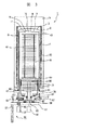
半導体製造プロセスの一つとして、シリコンウエハの酸化、拡散、CVD等を行う熱処理工程がある。この工程は、例えば図4に示すような縦型の半導体製造装置を使用して行われる。図4を用いて従来の縦型半導体製造装置について述べる。
【0003】
この縦型半導体製造装置1は、ヒータ2内に均熱管3が設けられ、均熱管3内に反応管20が設けられている。均熱管3は、熱伝導率の大きい材料、例えばSiC材で構成され、炉内の温度均一性を保つために使用する。ヒータ2は断熱材5で周囲を覆われている。
【0004】
反応管20は、反応管本体4と、1本のガス導入管(ガス導入通路)6とを備えている。反応管本体4の上側の天井板7上には上部ガス導入管8が設けられており、上部ガス導入管8と天井板7によりシャワー室9が構成されている。シャワー室9内の天井板7は、複数のガス分散孔10を有するガスシャワー板11となっており、シャワー室9はガスシャワー板11を介して反応管本体4の内部に連通している。
【0005】
ガス導入管6は、反応管本体4の外面に沿って鉛直方向に設けられており、その上流側である下端部にはガス導入部12が設けられ、下流側である上端は、反応管本体4の上部に設けられたシャワー室9に連通している。
【0006】
一方、反応管本体4の下端近傍には排気管30が連通して設けられている。そして、ガス導入管6のガス導入部12は反応ガス供給源(図示せず)に接続され、排気管30は排気装置(図示せず)に接続されている。
【0007】
反応管本体4は下端が開口して入口となっており、そこからボート40に装填された状態のウェハ41が導入、導出されるようになっている。ボート40は、ボートエレベータ50(アーム51及びギア52より成る)によって昇降されることで反応管本体4内に導入され、また、反応管本体4から取り出される。ボート40はキャップ60上に設置されており、キャップ60は炉口蓋61上に設けられている。また、反応管本体4の下端の周囲にはフランジ62が設けられており、フランジ62と炉口蓋61との間が、炉口蓋61を閉じたときにOリング63でシールされるようになっている。またキャップ60内部には、断熱材70(例えば石英ウール)が装填されている。
【0008】
前記ボート40は4本のボート支柱42を備えており、ボート支柱42には複数枚のウエハ41が水平姿勢で多段に装填され、その状態でウエハ41が熱処理されるようになっている。
【0009】
例えばウエハ41の酸化処理を行う場合は、ヒータ2により炉内およびウエハ41を酸化処理温度に加熱保持し、その状態で酸素ガスをガス導入管12によりシャワー室9に供給し、シャワー室9からガスシャワー板11のガス分散孔10を介して、反応管本体4内に分散供給する。そして、酸素ガスとウエハ41が反応して、ウエハ41の表面に酸化膜が形成される。ボート40を反応後のガスは排気管30を介して排気される。
【0010】
また、ウエハ41の面内温度分布を均一にさせるため、ボート40を回転させる機構が設置されている。すなわち、炉口蓋61及びアーム51を貫通した回転軸80に回転テーブル81が取付けられ、ボートエレベータ50が上昇することで、回転テーブル81がキャップ60の底を突き上げ、回転軸80に直結したモータ82の駆動により、ボート40が回転する。
【0011】
ところでウエハの熱処理に際しては、定常時のウエハ列の温度分布を設定温度±0.5℃の領域ができるだけ長くなるようにヒータの位置や発熱量を決めるが(この領域の長さを均熱長と称す)、ウエハ列の端、特にキャップ方向への放熱のため、急峻な温度分布が付く。従って、ウエハ列の端にはダミーウエハと呼ばれる、製品とはならないウエハを挿入しなければならない。しかしながら、ウエハの大口径化が進み、ウエハ自体が高価な為、従来のヒータ構造でダミーウエハとして用いればバッチ式の利点であるランニングコストを相殺してしまう。よって、キャップ部にヒータを設けることでウエハ列の下部からの放熱を補い、下向きの温度分布を小さくする。そうすることでウエハ列端のウエハを製品ウエハとして処理できるようになり、ランニングコストの低減が図れる。さらにキャップ内には断熱材が入っているが、これ自体が熱容量を大きくするため、温度の昇降に時間がかかる。これは高スループットの妨げになる。
【0012】
そこで特公平7−27874号公報記載のように、蓋体内部にヒータを配置した例、また特開平9−148315号公報記載のように、ウエハボートを載せる断熱基体の上部に石英ヒータを配列させることで熱処理領域から炉口への断熱効果を図っている。また特開平11−97446公報記載のように、昇降機構のアーム部に加熱ランプを配置し、ボート下部の薄い板を加熱させることで、昇温を迅速にし、ウエハ面内の均一性を向上させている。
【0013】
【発明が解決しようとする課題】
しかしながら上記従来技術では、石英ヒータ直上のウエハが石英ヒータのヒータパターンの影響を受け易いので均一とならないこと、また温度分布を均一にさせるためにはウエハを回転させることが有効であるが、この構成のまま回転させると、石英ヒータへの給電線がよじれてしまう。また、昇降機構のアーム部に加熱ランプを設置させると、アーム自体の構造が複雑かつ重くなり、かつ加熱ランプは切れ易いので、信頼性及びランプ交換の作業性の面で難がある。
【0014】
本発明の目的は、キャップ内の石英ヒータも発熱させることにより、昇温時間を短縮して高スループット化を図り、かつ、キャップ下方への放熱を防いで、定常時のウエハ列を全て均熱長区間に入れることでダミーウエハを不要とし、さらに、ウエハを回転させることにより、ウエハ面内での温度均一性に優れた半導体製造装置および半導体装置の製造方法を提供することにある。
【0015】
【課題を解決するための手段】
上記目的は、ボートに装填した半導体ウエハを加熱炉内に設けた反応管内の下端開口部より管軸方向に挿入搬出される半導体製造装置において、前記ボートの下部にあるキャップ内にヒータを有し、ボートの回転機構を備えることで達成される。
【0016】
また、前記ヒータに電源を供給するため、スリップリングを具備することで達成される。
【0017】
また、前記キャップの側面にヒータ、放射シールドを具備することで達成される。
【0018】
【発明の実施の形態】
図1に、本発明の第一実施例を示す縦型の半導体製造装置の断面図を示す。ここでは図4に示した従来の半導体製造装置と同じ要素に同符号を付して説明を簡略化する。
【0019】
この構造は、石英板等に形成された板状のヒータ90を固定させ、ウエハ41を積載したボート40を回転させるようにしたものである。キャップ60内にある板状のヒータ90は、アーム51に支柱91で固着される。キャップ60と掴んでいる回転テーブル81は、支柱91との軸受94、及び炉口蓋61との軸受95、及びアーム51との軸受96と各々組み合わされることで回転可能となっており、キャップ60は、モータ82、回転軸80、ベルト83、及び回転テーブル81を介して回転させる。なお、本実施例ではベルト83を介した回転機構としているが、回転機構の方式はこれに限るものではない。
【0020】
軸受96は反応管本体4内のボート40、積載されたウエハ41、ボート支柱42、キャップ60及び回転テーブル81の鉛直方向の荷重を受けている。板状のヒータ90への給電は、電源92より支柱91内に通した給電線93を介して成される。また、板状のヒータ90の下部には、下部への放射熱損失を低減させるために、熱遮蔽板(シリコンウエハ、もしくはSiC等)71を数枚配置する。
【0021】
反応管本体4にボート40に装填された状態のウェハ41を導入後、ヒータ2の他、板状のヒータ90も発熱させることで昇温時間が短縮でき、かつキャップ方向への放熱を防げるので、定常時のウエハ列を全て均熱長区間に入れることが出来、ダミーウエハが不要となる。また、ボート40を回転させるので、ウエハ41の面内温度分布が均一になる
本発明の参考例を、図2に示す。
図1の実施例では板状のヒータ90を固定させ、ウエハ41を積載したボート40を回転させている。これに対して図2に示した参考例では、回転軸80の内部に給電線93を設け、回転軸80にスリップリング97を設け、さらに電源92とスリップリング97とを給電線98で接続している。こうすることで、回転軸80に直結したモータ82の駆動により、ボート40及び板状のヒータ90とが回転し、かつ板状のヒータ90が電源92、給電線98、スリップリング97、給電線93を通じて加熱される。
【0022】
本発明のさらに他の実施例を、図3に示す。この図3に示した実施例では、キャップ60の放射熱損失をさらに防ぐために、キャップ60の側面部まで板状のヒータ90を設置し、さらにキャップ60に放射シールド72も設置している。これにより、キャップ側面への漏熱を低減でき、断熱効率がさらに向上する。
【0023】
【発明の効果】
以上の如く、本発明によれば、キャップ内の板状のヒータも発熱させることで昇温時間が短縮でき、かつキャップ下方への放熱を防げるので、定常時のウエハ列を全て均熱長区間に入れることが出来、ダミーウエハが不要となる。さらにウエハを回転させるので、ウエハ面内での温度均一性に優れた半導体製造装置を提供できる。
【図面の簡単な説明】
【図1】本発明の第一実施例を説明する半導体製造装置の断面図である。
【図2】 本発明の参考例を説明する半導体製造装置の断面図である。
【図3】本発明の他の実施例を説明する半導体製造装置の断面図である。
【図4】従来の半導体製造装置を示す断面図である。
【符号の説明】
1…縦型半導体製造装置、2…ヒータ、3…均熱管、4…反応管本体、5…断熱材、6…ガス導入管、7…天井板、8…上部ガス導入管、9…シャワー室、10…ガス分散孔、11…ガスシャワー室、12…ガス導入部、30…排気管、40…ボート、41…ウエハ、42…ボート支柱、50…ボートエレベータ、51…アーム、52…ギア、60…キャップ、61…炉口蓋、62…フランジ、63…Oリング、70…断熱材、71…熱遮蔽板、72…放射シールド、80…回転軸、81…回転テーブル、82…モータ、90…板状のヒータ、91…支柱、92…電源、93…給電線、94…軸受、95…軸受、96…軸受、97…スリップリング、98…給電線。[0001]
BACKGROUND OF THE INVENTION
The present invention relates to a manufacturing method of a semiconductor manufacturing apparatus and a semiconductor device that performs heat treatment of the semiconductor wafer.
[0002]
[Prior art]
As one of semiconductor manufacturing processes, there is a heat treatment process for performing oxidation, diffusion, CVD, etc. of a silicon wafer. This step is performed using, for example, a vertical semiconductor manufacturing apparatus as shown in FIG. A conventional vertical semiconductor manufacturing apparatus will be described with reference to FIG.
[0003]
In the vertical
[0004]
The
[0005]
The
[0006]
On the other hand, an
[0007]
The reaction tube
[0008]
The
[0009]
For example, when performing the oxidation process of the
[0010]
In order to make the in-plane temperature distribution of the
[0011]
By the way, in the heat treatment of the wafer, the position of the heater and the amount of heat generation are determined so that the temperature distribution of the wafer row in the steady state is as long as possible in the region where the set temperature ± 0.5 ° C. ) Due to heat dissipation toward the end of the wafer row, particularly in the cap direction, a steep temperature distribution is attached. Therefore, a wafer called a dummy wafer, which is not a product, must be inserted at the end of the wafer row. However, since the diameter of the wafer has been increased and the wafer itself is expensive, if it is used as a dummy wafer in the conventional heater structure, the running cost, which is an advantage of the batch method, is offset. Therefore, by providing a heater in the cap portion, heat dissipation from the lower part of the wafer row is compensated, and the downward temperature distribution is reduced. By doing so, the wafer at the end of the wafer row can be processed as a product wafer, and the running cost can be reduced. In addition, a heat insulating material is contained in the cap, but since this increases the heat capacity itself, it takes time to raise and lower the temperature. This hinders high throughput.
[0012]
Therefore, as described in Japanese Patent Publication No. 7-27874, an example in which a heater is arranged inside the lid body, and as disclosed in Japanese Patent Laid-Open No. 9-148315, a quartz heater is arranged on the heat insulating substrate on which the wafer boat is placed. In this way, the heat insulation effect from the heat treatment region to the furnace port is achieved. Further, as described in JP-A-11-97446, a heating lamp is arranged on the arm portion of the lifting mechanism, and a thin plate at the bottom of the boat is heated, so that the temperature rises quickly and the uniformity within the wafer surface is improved. ing.
[0013]
[Problems to be solved by the invention]
However, in the above prior art, the wafer just above the quartz heater is easily affected by the heater pattern of the quartz heater, so it is not uniform, and it is effective to rotate the wafer to make the temperature distribution uniform. If it rotates with a structure, the electric power feeding line to a quartz heater will be twisted. Further, if a heating lamp is installed in the arm portion of the lifting mechanism, the structure of the arm itself becomes complicated and heavy, and the heating lamp is easily cut off, which is difficult in terms of reliability and workability for lamp replacement.
[0014]
An object of the present invention, by also quartz heater in the cap to generate heat, to shorten the Atsushi Nobori time achieving high throughput and prevent heat radiation to the cap downward, soaking all wafer column in the steady state and unnecessary dummy wafer by placing a long interval, further, by rotating the wafer, is to provide a manufacturing method of a semiconductor manufacturing apparatus and semiconductor device with excellent temperature uniformity in the wafer plane.
[0015]
[Means for Solving the Problems]
The object is to provide a semiconductor manufacturing apparatus in which a semiconductor wafer loaded in a boat is inserted and unloaded in a tube axis direction from a lower end opening in a reaction tube provided in a heating furnace, and a heater is provided in a cap at the bottom of the boat. This is achieved by providing a boat rotation mechanism.
[0016]
Further, this is achieved by providing a slip ring for supplying power to the heater.
[0017]
Further, this is achieved by providing a heater and a radiation shield on the side surface of the cap.
[0018]
DETAILED DESCRIPTION OF THE INVENTION
FIG. 1 is a sectional view of a vertical semiconductor manufacturing apparatus showing a first embodiment of the present invention. Here, the same components as those in the conventional semiconductor manufacturing apparatus shown in FIG.
[0019]
In this structure, a plate-
[0020]
The
[0021]
After introducing the
In the embodiment of FIG. 1, a plate-
[0022]
Yet another embodiment of the present invention is shown in FIG. In the embodiment shown in FIG. 3, in order to further prevent radiant heat loss of the
[0023]
【The invention's effect】
As described above, according to the present invention, the plate-shaped heater in the cap can also generate heat so that the temperature rise time can be shortened and heat radiation to the bottom of the cap can be prevented. And no dummy wafer is required. Furthermore, since the wafer is rotated, it is possible to provide a semiconductor manufacturing apparatus with excellent temperature uniformity within the wafer surface.
[Brief description of the drawings]
FIG. 1 is a cross-sectional view of a semiconductor manufacturing apparatus illustrating a first embodiment of the present invention.
FIG. 2 is a cross-sectional view of a semiconductor manufacturing apparatus for explaining a reference example of the present invention.
FIG. 3 is a cross-sectional view of a semiconductor manufacturing apparatus for explaining another embodiment of the present invention.
FIG. 4 is a cross-sectional view showing a conventional semiconductor manufacturing apparatus.
[Explanation of symbols]
DESCRIPTION OF
Claims (5)
前記ボートが設置されるキャップと、
該キャップの下部を掴む回転テーブルと、
前記キャップ内で支柱に固定され、該支柱内に通した給電線を介して給電される前記キャップの内部の上部から横方向に伸び側面まで延在して設けられている板状のヒータと、
前記回転テーブルと前記支柱との間に設けられた軸受と、
前記下端開口部を閉じる炉口蓋と、
前記回転テーブルと前記炉口蓋との間に設けられる軸受と、
少なくとも前記板状のヒータおよび前記支柱は固定しつつ、前記ボートと前記キャップと前記回転テーブルとを回転させる回転機構と、
を備えたことを特徴とする半導体製造装置。In a semiconductor manufacturing apparatus in which a semiconductor wafer loaded in a boat is inserted and unloaded in a tube axis direction from a lower end opening in a reaction tube provided in a heater of a heating furnace,
A cap on which the boat is installed;
A rotary table for gripping the lower part of the cap;
A plate-like heater that is fixed to the support in the cap and is fed from the upper part of the cap that is fed through a power supply line passing through the support and extends in the lateral direction to the side surface;
A bearing provided between the rotary table and the support column;
A furnace lid that closes the lower end opening;
A bearing provided between the rotary table and the furnace cover;
A rotation mechanism that rotates the boat , the cap, and the turntable while fixing at least the plate-like heater and the support ;
A semiconductor manufacturing apparatus comprising:
前記回転テーブルと前記アームとの間に軸受が設けられていることを特徴とする請求項1記載の半導体製造装置。 A boat elevator having an arm for inserting a semiconductor wafer loaded in the boat into a tube axis direction from a lower end opening in the reaction tube;
The semiconductor manufacturing apparatus according to claim 1 , wherein a bearing is provided between the rotary table and the arm .
徴とする請求項1または2記載の半導体製造装置。 The semiconductor manufacturing apparatus according to claim 1 , wherein a plurality of heat shielding plates are arranged in the cap and below the heater .
前記ヒータおよび前記板状のヒータを発熱させて前記回転機構により少なくとも前記ヒータおよび前記支柱は固定しつつ、前記ボートと前記キャップと前記回転テーブルとを回転させて前記半導体ウエハを熱処理することを特徴とする半導体装置の製造方法。 The semiconductor wafer is heat-treated by causing the heater and the plate-like heater to generate heat and rotating the boat, the cap, and the turntable while fixing at least the heater and the support by the rotation mechanism. A method for manufacturing a semiconductor device.
Priority Applications (1)
| Application Number | Priority Date | Filing Date | Title |
|---|---|---|---|
| JP2002014962A JP3863786B2 (en) | 2002-01-24 | 2002-01-24 | Semiconductor manufacturing apparatus and semiconductor device manufacturing method |
Applications Claiming Priority (1)
| Application Number | Priority Date | Filing Date | Title |
|---|---|---|---|
| JP2002014962A JP3863786B2 (en) | 2002-01-24 | 2002-01-24 | Semiconductor manufacturing apparatus and semiconductor device manufacturing method |
Publications (3)
| Publication Number | Publication Date |
|---|---|
| JP2003218040A JP2003218040A (en) | 2003-07-31 |
| JP2003218040A5 JP2003218040A5 (en) | 2005-08-04 |
| JP3863786B2 true JP3863786B2 (en) | 2006-12-27 |
Family
ID=27651496
Family Applications (1)
| Application Number | Title | Priority Date | Filing Date |
|---|---|---|---|
| JP2002014962A Expired - Lifetime JP3863786B2 (en) | 2002-01-24 | 2002-01-24 | Semiconductor manufacturing apparatus and semiconductor device manufacturing method |
Country Status (1)
| Country | Link |
|---|---|
| JP (1) | JP3863786B2 (en) |
Families Citing this family (9)
| Publication number | Priority date | Publication date | Assignee | Title |
|---|---|---|---|---|
| US9018567B2 (en) * | 2011-07-13 | 2015-04-28 | Asm International N.V. | Wafer processing apparatus with heated, rotating substrate support |
| JP6605398B2 (en) * | 2015-08-04 | 2019-11-13 | 株式会社Kokusai Electric | Substrate processing apparatus, semiconductor manufacturing method, and program |
| TWI611043B (en) | 2015-08-04 | 2018-01-11 | Hitachi Int Electric Inc | Substrate processing apparatus, manufacturing method of semiconductor device, and recording medium |
| WO2018150537A1 (en) * | 2017-02-17 | 2018-08-23 | 株式会社Kokusai Electric | Substrate treatment device, method for manufacturing semiconductor device, and program |
| KR20190109216A (en) * | 2018-03-15 | 2019-09-25 | 가부시키가이샤 코쿠사이 엘렉트릭 | Substrate processing apparatus and method of manufacturing semiconductor device |
| US10714362B2 (en) | 2018-03-15 | 2020-07-14 | Kokusai Electric Corporation | Substrate processing apparatus and method of manufacturing semiconductor device |
| JP7463211B2 (en) | 2020-06-26 | 2024-04-08 | 株式会社フェローテックマテリアルテクノロジーズ | Angle adjustment device and rotation transmission mechanism |
| CN215925072U (en) * | 2020-09-24 | 2022-03-01 | 株式会社国际电气 | Substrate processing apparatus |
| WO2023097609A1 (en) * | 2021-12-02 | 2023-06-08 | 盛美半导体设备(上海)股份有限公司 | High-temperature tube furnace |
-
2002
- 2002-01-24 JP JP2002014962A patent/JP3863786B2/en not_active Expired - Lifetime
Also Published As
| Publication number | Publication date |
|---|---|
| JP2003218040A (en) | 2003-07-31 |
Similar Documents
| Publication | Publication Date | Title |
|---|---|---|
| JP3598032B2 (en) | Vertical heat treatment apparatus, heat treatment method, and heat insulation unit | |
| US6737613B2 (en) | Heat treatment apparatus and method for processing substrates | |
| JP3230836B2 (en) | Heat treatment equipment | |
| WO2006030857A1 (en) | Heat treatment apparatus and substrate manufacturing method | |
| JP3863786B2 (en) | Semiconductor manufacturing apparatus and semiconductor device manufacturing method | |
| JP2012033871A (en) | Substrate processing apparatus, method of manufacturing semiconductor device and heating apparatus | |
| US20090197402A1 (en) | Substrate processing apparatus, method for manufacturing semiconductor device, and process tube | |
| TWI780314B (en) | Substrate heating apparatus and substrate processing apparatus using the same | |
| JP2007073865A (en) | Heat treatment device | |
| JPH10242067A (en) | Substrate supporting tool for heat treatment | |
| JP3904497B2 (en) | Manufacturing method of semiconductor device | |
| KR20030074418A (en) | Substrate processing method and apparatus | |
| JP2002305189A (en) | Vertical heat treatment apparatus and method for forcible air cooling | |
| JP4115331B2 (en) | Substrate processing equipment | |
| JP2005123284A (en) | Semiconductor manufacturing device | |
| JP2010199493A (en) | Substrate treatment device | |
| JP2008218877A (en) | Substrate treatment device and method of manufacturing semiconductor device | |
| JP2013038128A (en) | Heat treatment apparatus | |
| KR100350612B1 (en) | Dual Vertical Heat Treatment Furnace | |
| JP5006821B2 (en) | Substrate processing apparatus and semiconductor device manufacturing method | |
| JP2005217317A (en) | Substrate processing equipment | |
| JP2010093069A (en) | Heat treatment apparatus of substrate | |
| JP2004023049A (en) | Heat treatment equipment | |
| JPH0468522A (en) | Vertical heat treatment device | |
| JP2006080256A (en) | Substrate processing apparatus |
Legal Events
| Date | Code | Title | Description |
|---|---|---|---|
| A521 | Request for written amendment filed |
Free format text: JAPANESE INTERMEDIATE CODE: A523 Effective date: 20041227 |
|
| A621 | Written request for application examination |
Free format text: JAPANESE INTERMEDIATE CODE: A621 Effective date: 20041227 |
|
| A977 | Report on retrieval |
Free format text: JAPANESE INTERMEDIATE CODE: A971007 Effective date: 20060116 |
|
| A131 | Notification of reasons for refusal |
Free format text: JAPANESE INTERMEDIATE CODE: A131 Effective date: 20060124 |
|
| A521 | Request for written amendment filed |
Free format text: JAPANESE INTERMEDIATE CODE: A523 Effective date: 20060324 |
|
| A711 | Notification of change in applicant |
Free format text: JAPANESE INTERMEDIATE CODE: A711 Effective date: 20060324 |
|
| RD01 | Notification of change of attorney |
Free format text: JAPANESE INTERMEDIATE CODE: A7421 Effective date: 20060324 |
|
| A521 | Request for written amendment filed |
Free format text: JAPANESE INTERMEDIATE CODE: A821 Effective date: 20060324 |
|
| A521 | Request for written amendment filed |
Free format text: JAPANESE INTERMEDIATE CODE: A821 Effective date: 20060522 |
|
| A131 | Notification of reasons for refusal |
Free format text: JAPANESE INTERMEDIATE CODE: A131 Effective date: 20060704 |
|
| A521 | Request for written amendment filed |
Free format text: JAPANESE INTERMEDIATE CODE: A523 Effective date: 20060830 |
|
| TRDD | Decision of grant or rejection written | ||
| A01 | Written decision to grant a patent or to grant a registration (utility model) |
Free format text: JAPANESE INTERMEDIATE CODE: A01 Effective date: 20060926 |
|
| A61 | First payment of annual fees (during grant procedure) |
Free format text: JAPANESE INTERMEDIATE CODE: A61 Effective date: 20060929 |
|
| R150 | Certificate of patent or registration of utility model |
Ref document number: 3863786 Country of ref document: JP Free format text: JAPANESE INTERMEDIATE CODE: R150 Free format text: JAPANESE INTERMEDIATE CODE: R150 |
|
| FPAY | Renewal fee payment (event date is renewal date of database) |
Free format text: PAYMENT UNTIL: 20091006 Year of fee payment: 3 |
|
| FPAY | Renewal fee payment (event date is renewal date of database) |
Free format text: PAYMENT UNTIL: 20101006 Year of fee payment: 4 |
|
| FPAY | Renewal fee payment (event date is renewal date of database) |
Free format text: PAYMENT UNTIL: 20111006 Year of fee payment: 5 |
|
| FPAY | Renewal fee payment (event date is renewal date of database) |
Free format text: PAYMENT UNTIL: 20121006 Year of fee payment: 6 |
|
| FPAY | Renewal fee payment (event date is renewal date of database) |
Free format text: PAYMENT UNTIL: 20121006 Year of fee payment: 6 |
|
| FPAY | Renewal fee payment (event date is renewal date of database) |
Free format text: PAYMENT UNTIL: 20131006 Year of fee payment: 7 |
|
| R250 | Receipt of annual fees |
Free format text: JAPANESE INTERMEDIATE CODE: R250 |
|
| R250 | Receipt of annual fees |
Free format text: JAPANESE INTERMEDIATE CODE: R250 |
|
| R250 | Receipt of annual fees |
Free format text: JAPANESE INTERMEDIATE CODE: R250 |
|
| S111 | Request for change of ownership or part of ownership |
Free format text: JAPANESE INTERMEDIATE CODE: R313111 |
|
| S531 | Written request for registration of change of domicile |
Free format text: JAPANESE INTERMEDIATE CODE: R313531 |
|
| R350 | Written notification of registration of transfer |
Free format text: JAPANESE INTERMEDIATE CODE: R350 |
|
| R250 | Receipt of annual fees |
Free format text: JAPANESE INTERMEDIATE CODE: R250 |
|
| EXPY | Cancellation because of completion of term |