JP3858801B2 - In-vehicle millimeter-wave radar device, millimeter-wave radar module, and manufacturing method thereof - Google Patents
In-vehicle millimeter-wave radar device, millimeter-wave radar module, and manufacturing method thereof Download PDFInfo
- Publication number
- JP3858801B2 JP3858801B2 JP2002296872A JP2002296872A JP3858801B2 JP 3858801 B2 JP3858801 B2 JP 3858801B2 JP 2002296872 A JP2002296872 A JP 2002296872A JP 2002296872 A JP2002296872 A JP 2002296872A JP 3858801 B2 JP3858801 B2 JP 3858801B2
- Authority
- JP
- Japan
- Prior art keywords
- millimeter wave
- millimeter
- substrate
- wave radar
- radar module
- Prior art date
- Legal status (The legal status is an assumption and is not a legal conclusion. Google has not performed a legal analysis and makes no representation as to the accuracy of the status listed.)
- Expired - Fee Related
Links
Images


Classifications
-
- G—PHYSICS
- G01—MEASURING; TESTING
- G01S—RADIO DIRECTION-FINDING; RADIO NAVIGATION; DETERMINING DISTANCE OR VELOCITY BY USE OF RADIO WAVES; LOCATING OR PRESENCE-DETECTING BY USE OF THE REFLECTION OR RERADIATION OF RADIO WAVES; ANALOGOUS ARRANGEMENTS USING OTHER WAVES
- G01S7/00—Details of systems according to groups G01S13/00, G01S15/00, G01S17/00
- G01S7/02—Details of systems according to groups G01S13/00, G01S15/00, G01S17/00 of systems according to group G01S13/00
- G01S7/03—Details of HF subsystems specially adapted therefor, e.g. common to transmitter and receiver
- G01S7/032—Constructional details for solid-state radar subsystems
-
- G—PHYSICS
- G01—MEASURING; TESTING
- G01S—RADIO DIRECTION-FINDING; RADIO NAVIGATION; DETERMINING DISTANCE OR VELOCITY BY USE OF RADIO WAVES; LOCATING OR PRESENCE-DETECTING BY USE OF THE REFLECTION OR RERADIATION OF RADIO WAVES; ANALOGOUS ARRANGEMENTS USING OTHER WAVES
- G01S13/00—Systems using the reflection or reradiation of radio waves, e.g. radar systems; Analogous systems using reflection or reradiation of waves whose nature or wavelength is irrelevant or unspecified
- G01S13/88—Radar or analogous systems specially adapted for specific applications
- G01S13/93—Radar or analogous systems specially adapted for specific applications for anti-collision purposes
- G01S13/931—Radar or analogous systems specially adapted for specific applications for anti-collision purposes of land vehicles
- G01S2013/9327—Sensor installation details
-
- H—ELECTRICITY
- H01—ELECTRIC ELEMENTS
- H01L—SEMICONDUCTOR DEVICES NOT COVERED BY CLASS H10
- H01L2224/00—Indexing scheme for arrangements for connecting or disconnecting semiconductor or solid-state bodies and methods related thereto as covered by H01L24/00
- H01L2224/01—Means for bonding being attached to, or being formed on, the surface to be connected, e.g. chip-to-package, die-attach, "first-level" interconnects; Manufacturing methods related thereto
- H01L2224/42—Wire connectors; Manufacturing methods related thereto
- H01L2224/47—Structure, shape, material or disposition of the wire connectors after the connecting process
- H01L2224/48—Structure, shape, material or disposition of the wire connectors after the connecting process of an individual wire connector
- H01L2224/4805—Shape
- H01L2224/4809—Loop shape
- H01L2224/48091—Arched
-
- H—ELECTRICITY
- H01—ELECTRIC ELEMENTS
- H01L—SEMICONDUCTOR DEVICES NOT COVERED BY CLASS H10
- H01L2924/00—Indexing scheme for arrangements or methods for connecting or disconnecting semiconductor or solid-state bodies as covered by H01L24/00
- H01L2924/15—Details of package parts other than the semiconductor or other solid state devices to be connected
- H01L2924/161—Cap
- H01L2924/1615—Shape
- H01L2924/16152—Cap comprising a cavity for hosting the device, e.g. U-shaped cap
Description
【0001】
【発明の属する技術分野】
本発明は、車載ミリ波レーダ装置,ミリ波レーダモジュールおよび製造方法に関するものである。
【0002】
【従来の技術】
特許文献1ではIC部を中空構造とするために、その外側にキャップを設けて、ICが樹脂封止による熱応力により、ボンデキングワイヤが切断することを防止している。
【0003】
【特許文献1】
特開平7−273237号公報
【0004】
【発明が解決しようとする課題】
上記の従来技術は、高周波などのミリ波レーダ用RFモジュールにおいてミリ波電気特性の低下防止のための中空構造を成立させ、かつ耐湿性とを両立に配慮がされておらず、安価なミリ波レーダ用RFモジュールが提供できない問題があった。
【0005】
本発明の目的は、中空構造と耐湿性とを両立させたミリ波レーダ装置およびモジュールを実現することにある。
【0006】
【課題を解決するための手段】
上記目的は、車載ミリ波レーダ装置において、ミリ波を発生するミリ波発生手段と、前記ミリ波発生手段が設置される基板と、前記基板に接合され、前記基板と共に前記ミリ波発生手段を収容する中空部を形成する囲いを成す部材と、前記接合部を覆うゲル状耐湿性レジンとを備えることによって達成される。
【0007】
ミリ波用MMICが搭載される多層基板と中空を形成するためのキャップとを接着剤などの有機部材で接合して高周波特性を確保し、その全体を収納するケース中に耐湿性のゲル状の有機レジンで覆う構造として、気密性を有しない構造として、安価な部材の使用と生産性向上を実現するものである。
【0008】
また、上記目的は、MMICにより発生したレーダ波をアンテナパターンを介して発信するミリ波レーダモジュールの製造方法であって、(a)配線を有する基板に前記MMICを設置し、(b)中空部を有するキャップを、前記MMICが前記中空部に位置するように、前記基板に接合して前記MMICを囲い、(c)ゲルにより前記接合された部分を覆ったことによって達成される。
【0009】
【発明の実施の形態】
以下、本発明の実施例を図1により説明する。
【0010】
アンテナパターン2と一体に形成された多層基板1上にMMIC10,11やパッド13をはんだ接合,ワイヤボンディングされて回路を形成している。
【0011】
本回路をキャップ50を有機接着剤60で接合して、前記MMIC10,11の回路部を中空構造としている。
【0012】
本中空構造の形成においては、前記キャップ50の接合工程を窒素ガス中で行い窒素ガスなどの封止ガス100を封止しても良い。
【0013】
また、中空構造部に湿度吸収部剤(図示せず)を収納して、前記MMICを湿度から保護するようにしても良い。
【0014】
前記の多層基板1は、金属端子30がインサートされたプラスチックケース40に有機接着剤60で接合し、前記パッド15と前記金属端子30とワイヤ20で接続した後に、シリコーン系などのゲル70を充填している。
【0015】
本構造の実施例によれば、MMIC部の簡易気密封止の中空構造により、ミリ波などの高周波電気特性を確保し、湿度についてはゲル剤で保護できる効果がある。
【0016】
図2は他の実施例であるが、図1に比べてプラスチックカバー80をプラスチックケース40と有機接着剤60で接合することにより、実施例の図1に比べて耐湿性が高い効果がある。
【0017】
図3の実施例は図1に対して、金属製ケース41を用いるために金属端子30を絶縁するためにガラスなどの絶縁物45を用いたものである。このような構成とすることにより、多層基板1と金属製ケース41の熱線膨張係数の差を少なくでき、この結果、温度サイクルなどの熱ストレスにより、多層基板1と金属製ケース41間にクラックの発生がなく、耐湿性が向上する効果がある。
【0018】
図4は、図1から図3の実施例が、多層基板1とケース40,41が分離構造なのに対して、一体化42したものである。
【0019】
このようにすることにより、安価にできる効果がある。
【0020】
一体化構造42の形成は、コストの点から有機材料が望ましいが、無機材料での形成でも良い。
【0021】
図5の実施例は図4に対して、アンテナパターン2の分離構造である。このようにすることにより、アンテナ特性の自由度が増す効果がある。
【0022】
図6の実施例は、無機質の多層基板3を構成する製法上の部材を多層基板1A,その部材1Bで構成し、金属カバー51をはんだ等のろう材65で封止することにより、中空部の気密性が確保できる効果がある。
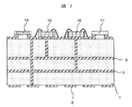
【0023】
図7は、多層基板1の一実施例を示すもので、MMICチップ15,マイコンチップ16,クロック発振子17,フィルタコンデンサ18を搭載し、アナログ信号グランド6やデジタル信号グランド5など信号分離を施してある。多層基板1の半対面にはアンテナパターン2を形成してある。
【0024】
このような構成によれば、ミリ波レーダ全体をモジュール化することができる効果がある。
【0025】
【発明の効果】
以上のように本発明によれば、ミリ波用MMICが搭載された多層基板を中空構造とすることができるために、ミリ波電気特性を確保でき、その全体を収納するケース中に耐湿性のゲル状の有機レジンでで覆う構造のため、気密性を有しなくてもミリ波電気特性を確保しつつ、生産性をも向上した安価なミリ波レーダ用RFモジュールが提供できる効果がある。
【図面の簡単な説明】
【図1】本発明の実施例の断面構造図である。
【図2】本発明の他の実施例である。
【図3】本発明の他の実施例である。
【図4】本発明の他の実施例である。
【図5】本発明の他の実施例である。
【図6】本発明の他の実施例である。
【図7】本発明の構造に用いた多層基板の実施例である。
【符号の説明】
1…多層基板、2…アンテナパターン、10,11…MMIC、13…パッド、20…ワイヤ、30…金属端子、40…プラスチックケース、50…キャップ、70…ゲル、100…封止ガス。[0001]
BACKGROUND OF THE INVENTION
The present invention relates to an in-vehicle millimeter wave radar device, a millimeter wave radar module, and a manufacturing method.
[0002]
[Prior art]
In
[0003]
[Patent Document 1]
JP-A-7-273237 [0004]
[Problems to be solved by the invention]
The above-mentioned prior art has established a hollow structure for preventing the deterioration of millimeter-wave electrical characteristics in an RF module for millimeter-wave radar such as high frequency, and is not considered to be compatible with moisture resistance. There was a problem that the radar RF module could not be provided.
[0005]
An object of the present invention is to realize a millimeter wave radar device and a module that have both a hollow structure and moisture resistance.
[0006]
[Means for Solving the Problems]
In the in- vehicle millimeter-wave radar device, the object is to provide millimeter-wave generation means for generating millimeter waves, a substrate on which the millimeter-wave generation means is installed, and the millimeter-wave generation means that is bonded to the substrate and accommodates the substrate. This is achieved by including a member forming an enclosure that forms a hollow portion and a gel-like moisture-resistant resin that covers the joint portion .
[0007]
A multilayer substrate on which the millimeter wave MMIC is mounted and a cap for forming a hollow are joined with an organic member such as an adhesive to ensure high frequency characteristics, and a moisture-resistant gel-like case is housed in the case housing the whole. As a structure that is covered with an organic resin, a structure that does not have airtightness is realized, and an inexpensive member is used and productivity is improved.
[0008]
Another object of the present invention is to provide a method for manufacturing a millimeter wave radar module that transmits a radar wave generated by an MMIC via an antenna pattern, wherein (a) the MMIC is installed on a substrate having wiring, and (b) a hollow portion. The cap having the following is achieved by bonding the MMIC to the substrate so that the MMIC is located in the hollow portion, and (c) covering the bonded portion with a gel.
[0009]
DETAILED DESCRIPTION OF THE INVENTION
An embodiment of the present invention will be described below with reference to FIG.
[0010]
On the
[0011]
In this circuit, the
[0012]
In forming this hollow structure, the joining process of the
[0013]
Further, a humidity absorbing agent (not shown) may be housed in the hollow structure portion to protect the MMIC from humidity.
[0014]
The
[0015]
According to the embodiment of the present structure, there is an effect that high-frequency electrical characteristics such as millimeter waves can be ensured and humidity can be protected with a gel agent by the simple airtight sealed hollow structure of the MMIC portion.
[0016]
FIG. 2 shows another embodiment. By joining the
[0017]
The embodiment of FIG. 3 uses an
[0018]
FIG. 4 shows an example in which the embodiment of FIGS. 1 to 3 is integrated 42 while the
[0019]
By doing in this way, there exists an effect which can be made cheap.
[0020]
The formation of the integrated
[0021]
The embodiment of FIG. 5 is a separation structure of the
[0022]
In the embodiment of FIG. 6, the manufacturing method member constituting the
[0023]
FIG. 7 shows an embodiment of the
[0024]
According to such a configuration, there is an effect that the entire millimeter wave radar can be modularized.
[0025]
【The invention's effect】
As described above, according to the present invention, since the multilayer substrate on which the MMIC for millimeter waves is mounted can have a hollow structure, the millimeter-wave electrical characteristics can be ensured, and the moisture-proof case can be contained in the case housing the whole. Since the structure is covered with a gel-like organic resin, it is possible to provide an inexpensive millimeter-wave radar RF module with improved productivity while ensuring millimeter-wave electrical characteristics without airtightness.
[Brief description of the drawings]
FIG. 1 is a sectional structural view of an embodiment of the present invention.
FIG. 2 is another embodiment of the present invention.
FIG. 3 is another embodiment of the present invention.
FIG. 4 is another embodiment of the present invention.
FIG. 5 is another embodiment of the present invention.
FIG. 6 is another embodiment of the present invention.
FIG. 7 is an example of a multilayer substrate used in the structure of the present invention.
[Explanation of symbols]
DESCRIPTION OF
Claims (26)
前記ミリ波発生手段が設置される基板と、
前記基板に接合され、前記基板と共に前記ミリ波発生手段を収容する中空部を形成する囲いを成す部材と、
前記基板と前記囲いを成す部材との接合部を覆うゲル状耐湿性レジンとを備えた車載ミリ波レーダ装置。Millimeter wave generating means for generating millimeter waves ,
A substrate on which the millimeter wave generating means is installed;
A member that is bonded to the substrate and forms a hollow portion that houses the millimeter wave generating means together with the substrate ;
An on- vehicle millimeter-wave radar device comprising a gel-like moisture-resistant resin that covers a joint portion between the substrate and the member that forms the enclosure .
前記基板に取り付けられ、前記接合部を収容する凹部を形成するケースを備え、A case that is attached to the substrate and includes a case that forms a recess that houses the joint;
前記ゲル状耐湿性レジンは、前記凹部に充填されることを特徴とする車載ミリ波レーダ装置。The vehicle-mounted millimeter-wave radar device, wherein the gel-like moisture-resistant resin is filled in the recess.
前記基板は、前記ミリ波発生手段が設置された面と反対側の面に、前記ミリ波を送信するアンテナ手段を備えることを特徴とする車載ミリ波レーダ装置。In claim 1 or 2 ,
The substrate, on the opposite side of the surface and the millimeter wave generating means installed surface, automotive millimeter wave radar apparatus characterized by comprising an antenna means for transmitting the millimeter wave.
前記中空部には、不活性ガスが充填されることを特徴とする車載ミリ波レーダ装置。In any one of Claims 1 thru | or 3 ,
It said hollow portion, automotive millimeter wave radar system which inert gas is equal to or that will be filled.
前記中空部には、湿気を吸収する手段を備えることを特徴とする車載ミリ波レ
ーダ装置。In any one of Claims 1 thru | or 3 ,
Said hollow portion, automotive millimeter wave radar system, characterized in that Ru comprising a means for absorbing moisture.
一方の面に前記ミリ波用MMICが搭載され、ミリ波用回路が形成された基板と、
前記基板の前記ミリ波用MMICが搭載される面と反対側の面に形成され、ミリ波電波を送受信するアンテナ回路と、
前記基板に接合され、前記ミリ波用MMICを収納する収納部を形成するキャップとを備え、
前記キャップの外側をゲル状耐湿性レジンで保護したミリ波レーダモジュール。 MMIC for millimeter wave,
A substrate on which the millimeter wave MMIC is mounted on one surface and a millimeter wave circuit is formed;
An antenna circuit that is formed on a surface of the substrate opposite to the surface on which the millimeter wave MMIC is mounted;
A cap bonded to the substrate and forming a storage portion for storing the MMIC for millimeter waves;
Millimeter-wave radar module protected with gel moisture resistance resin outside of the cap.
前記基板は、入出力信号端子が設けられたケースに収納され、The substrate is housed in a case provided with input / output signal terminals,
前記ゲル状耐湿性レジンは、前記ケースと前記基板とにより構成される凹部に充填されることを特徴とするミリ波レーダモジュール。The millimeter-wave radar module according to claim 1, wherein the gel-like moisture-resistant resin is filled in a recess formed by the case and the substrate.
前記ケースは、入出力信号端子がインサートされたプラスチックケースであることを特徴とするミリ波レーダモジュール。The millimeter wave radar module according to claim 1, wherein the case is a plastic case having input / output signal terminals inserted therein.
前記ケースは、入出力信号端子の周りに絶縁性材料を設けた導電性ケースであることを特徴とするミリ波レーダモジュール。In claim 6 ,
The millimeter wave radar module , wherein the case is a conductive case in which an insulating material is provided around an input / output signal terminal.
前記基板と前記プラスチックケースの形成を一体としたミリ波レーダモジュール。In claim 8 ,
A millimeter wave radar module in which the substrate and the plastic case are integrally formed.
前記ゲル状耐湿レジンの上に更に別部材のカバーを接合したミリ波レーダモジュール。In any one of Claims 6 thru | or 10 ,
A millimeter wave radar module in which a cover of another member is further joined on the gel-like moisture-resistant resin .
前記基板は、前記ミリ波用MMICを収納する空間を有する形状とし、
前記基板に平坦状のカバーを接合して、前記ミリ波用MMICの収納部を中空とするミリ波レーダモジュール。In claim 6 ,
The substrate has a shape having a space for accommodating the millimeter wave MMIC ,
By joining a flat cover on the substrate, the millimeter-wave radar module to hollow the housing portion of the MMIC for the millimeter wave.
前記基板には前記ミリ波用回路を形成して、前記アンテナ回路は前記ミリ波用回路とは別部材で形成したミリ波レーダモジュール。In any one of Claims 6 thru | or 12 ,
Wherein the substrate to form a circuit for the millimeter wave, the antenna circuit is a millimeter-wave radar module formed by a member separate from the circuit the millimeter wave.
前記ミリ波用MMICの収納部には、湿度吸収部材を収納したミリ波レーダモジュール。In any one of Claims 6 thru | or 12 ,
A millimeter wave radar module in which a humidity absorbing member is housed in the housing portion of the millimeter wave MMIC.
前記ミリ波用MMICの収納部は、不活性ガスを充填したミリ波レーダモジュール。In any one of Claims 6 thru | or 12 ,
The storage part of the millimeter wave MMIC is a millimeter wave radar module filled with an inert gas.
前記基板は無機質材か有機質材のいずれかで形成された多層基板であるミリ波レーダモジュール。In any one of Claims 6 thru | or 12 ,
The millimeter wave radar module, wherein the substrate is a multilayer substrate formed of either an inorganic material or an organic material.
前記キャップと前記基板とを有機部材で接合したミリ波レーダモジュール。In any one of Claims 6 thru | or 12 ,
Millimeter-wave radar module with bonding the said cap substrate with an organic material.
(a)配線を有する基板に前記MMICを設置し、
(b)中空部を有するキャップを、前記MMICが前記中空部に位置するように、前記基板に接合して前記MMICを囲い、
(c)ゲル状耐湿性レジンにより前記接合された部分を覆うことを特徴とするミリ波レーダモジュールの製造方法。A method of manufacturing a millimeter wave radar module for transmitting a radar wave generated by an MMIC via an antenna pattern,
(A) installing the MMIC on a substrate having wiring;
(B) A cap having a hollow part is joined to the substrate so that the MMIC is positioned in the hollow part, and the MMIC is enclosed.
(C) A method of manufacturing a millimeter wave radar module, wherein the joined portion is covered with a gel- like moisture-resistant resin .
前記接合は、窒素ガス雰囲気中で行われることを特徴とするミリ波レーダモジュールの製造方法。In claim 18 ,
The bonding method of manufacturing a millimeter-wave radar module, wherein the Ru conducted in a nitrogen gas atmosphere.
前記基板には囲いを成す壁が設けられ、
前記接合後に、前記ゲル状耐湿性レジンが前記囲いの中に注がれることを特徴とするミリ波レーダモジュールの製造方法。In claim 18 ,
The substrate is provided with an enclosing wall,
A manufacturing method of a millimeter wave radar module, wherein the gel- like moisture-resistant resin is poured into the enclosure after the joining.
前記多層基板は、ミリ波電波を送受信するパッチアンテナ回路が形成され、他の面には、ミリ波用MMICの回路が形成され、かつ前記多層基板は入出力信号端子がインサートされたプラスチックケースに収納され、かつ前記多層基板は平面形状ではなく、空間を有する形状とし、前記多層基板に平坦状のカバーを接合して、前記ミリ波用MMICを収納する中空の収納部を形成し、前記カバーの上を耐湿レジンで保護したミリ波レーダモジュール。In a millimeter wave radar module with a millimeter wave MMIC mounted on a multilayer substrate,
The multilayer substrate is formed with a patch antenna circuit for transmitting and receiving millimeter wave radio waves, the other surface is formed with a millimeter wave MMIC circuit, and the multilayer substrate is formed in a plastic case in which input / output signal terminals are inserted. The multilayer substrate is housed in a shape having a space rather than a planar shape, and a flat cover is joined to the multilayer substrate to form a hollow housing portion for housing the millimeter wave MMIC, and the cover A millimeter-wave radar module with a moisture-resistant resin on top.
前記多層基板には前記ミリ波用回路を形成して、前記アンテナ回路は前記ミリ波用回路とは別部材で形成したミリ波レーダモジュール。A millimeter wave radar module in which the millimeter wave circuit is formed on the multilayer substrate, and the antenna circuit is formed of a member different from the millimeter wave circuit.
前記ミリ波用MMICの収納部には、湿度吸収部材を収納したミリ波レーダモジュール。A millimeter wave radar module in which a humidity absorbing member is housed in the housing portion of the millimeter wave MMIC.
前記ミリ波用MMICの収納部は、不活性ガスを充填したミリ波レーダモジュール。The storage part of the millimeter wave MMIC is a millimeter wave radar module filled with an inert gas.
前記多層基板は無機質材か有機質材のいずれかで形成されるミリ波レーダモジュール。The multilayer substrate is a millimeter wave radar module formed of either an inorganic material or an organic material.
前記カバーと前記多層基板とを有機部材で接合したミリ波レーダモジュール。A millimeter-wave radar module in which the cover and the multilayer substrate are joined with an organic member.
Priority Applications (4)
| Application Number | Priority Date | Filing Date | Title |
|---|---|---|---|
| JP2002296872A JP3858801B2 (en) | 2002-10-10 | 2002-10-10 | In-vehicle millimeter-wave radar device, millimeter-wave radar module, and manufacturing method thereof |
| US10/681,246 US7098842B2 (en) | 2002-10-10 | 2003-10-09 | Vehicle-mounted millimeter wave radar device, millimeter wave radar module, and manufacturing method thereof |
| EP03022982A EP1422534A1 (en) | 2002-10-10 | 2003-10-10 | Vehicle-mounted millimeter wave radar device, millimeter wave radar module, and manufacturing method thereof |
| US11/482,056 US7355547B2 (en) | 2002-10-10 | 2006-07-07 | Vehicle-mounted millimeter wave radar device, millimeter wave radar module, and manufacturing method thereof |
Applications Claiming Priority (1)
| Application Number | Priority Date | Filing Date | Title |
|---|---|---|---|
| JP2002296872A JP3858801B2 (en) | 2002-10-10 | 2002-10-10 | In-vehicle millimeter-wave radar device, millimeter-wave radar module, and manufacturing method thereof |
Publications (2)
| Publication Number | Publication Date |
|---|---|
| JP2004134541A JP2004134541A (en) | 2004-04-30 |
| JP3858801B2 true JP3858801B2 (en) | 2006-12-20 |
Family
ID=32089248
Family Applications (1)
| Application Number | Title | Priority Date | Filing Date |
|---|---|---|---|
| JP2002296872A Expired - Fee Related JP3858801B2 (en) | 2002-10-10 | 2002-10-10 | In-vehicle millimeter-wave radar device, millimeter-wave radar module, and manufacturing method thereof |
Country Status (3)
| Country | Link |
|---|---|
| US (2) | US7098842B2 (en) |
| EP (1) | EP1422534A1 (en) |
| JP (1) | JP3858801B2 (en) |
Cited By (1)
| Publication number | Priority date | Publication date | Assignee | Title |
|---|---|---|---|---|
| KR20100051270A (en) * | 2008-11-07 | 2010-05-17 | 시빔, 인코퍼레이티드 | Surface mountable integrated circuit packaging scheme |
Families Citing this family (23)
| Publication number | Priority date | Publication date | Assignee | Title |
|---|---|---|---|---|
| DE102004029440A1 (en) * | 2004-06-18 | 2006-01-12 | Infineon Technologies Ag | Transmitting / receiving device |
| JP4189970B2 (en) * | 2004-11-05 | 2008-12-03 | 株式会社日立製作所 | Antenna device |
| US8106307B2 (en) * | 2006-01-26 | 2012-01-31 | Panasonic Corporation | Substrate structure and electronic apparatus |
| IL173941A0 (en) * | 2006-02-26 | 2007-03-08 | Haim Goldberger | Monolithic modules for high frequecney applications |
| JP4286855B2 (en) * | 2006-09-07 | 2009-07-01 | 株式会社日立製作所 | Radar equipment |
| US7492313B1 (en) * | 2006-10-31 | 2009-02-17 | Lockheed Martin Corporation | Digital processing radar system |
| US7675465B2 (en) * | 2007-05-22 | 2010-03-09 | Sibeam, Inc. | Surface mountable integrated circuit packaging scheme |
| US8345716B1 (en) | 2007-06-26 | 2013-01-01 | Lockheed Martin Corporation | Polarization diverse antenna array arrangement |
| US7705761B2 (en) * | 2007-11-07 | 2010-04-27 | Lockheed Martin Corporation | System and method for wideband direct sampling and beamforming using complex analog to digital converter |
| US7830301B2 (en) * | 2008-04-04 | 2010-11-09 | Toyota Motor Engineering & Manufacturing North America, Inc. | Dual-band antenna array and RF front-end for automotive radars |
| US7733265B2 (en) * | 2008-04-04 | 2010-06-08 | Toyota Motor Engineering & Manufacturing North America, Inc. | Three dimensional integrated automotive radars and methods of manufacturing the same |
| US8022861B2 (en) * | 2008-04-04 | 2011-09-20 | Toyota Motor Engineering & Manufacturing North America, Inc. | Dual-band antenna array and RF front-end for mm-wave imager and radar |
| US7990237B2 (en) * | 2009-01-16 | 2011-08-02 | Toyota Motor Engineering & Manufacturing North America, Inc. | System and method for improving performance of coplanar waveguide bends at mm-wave frequencies |
| US8786496B2 (en) | 2010-07-28 | 2014-07-22 | Toyota Motor Engineering & Manufacturing North America, Inc. | Three-dimensional array antenna on a substrate with enhanced backlobe suppression for mm-wave automotive applications |
| US8279100B2 (en) | 2010-09-30 | 2012-10-02 | Lockheed Martin Corporation | Complex analog to digital converter (CADC) system on chip double rate architecture |
| US8854255B1 (en) | 2011-03-28 | 2014-10-07 | Lockheed Martin Corporation | Ground moving target indicating radar |
| BR112013028804B1 (en) * | 2012-10-03 | 2020-11-17 | Shindengen Electric Manufacturing Co., Ltd. | electronic device |
| DE102014109120B4 (en) | 2014-06-30 | 2017-04-06 | Krohne Messtechnik Gmbh | microwave module |
| US10411329B2 (en) | 2016-01-20 | 2019-09-10 | Apple Inc. | Packaged devices with antennas |
| WO2018092922A1 (en) * | 2016-11-15 | 2018-05-24 | 인지니어스 주식회사 | Radar module comprising blocking substrate |
| US10910706B2 (en) * | 2018-01-19 | 2021-02-02 | Mediatek Inc. | Radar sensor housing design |
| US20220059936A1 (en) * | 2018-05-10 | 2022-02-24 | Richwave Technology Corp. | Doppler motion sensor device with high isolation between antennas |
| JP7211333B2 (en) * | 2019-10-30 | 2023-01-24 | 株式会社デンソー | Electronics |
Family Cites Families (10)
| Publication number | Priority date | Publication date | Assignee | Title |
|---|---|---|---|---|
| JP2710207B2 (en) | 1994-03-30 | 1998-02-10 | 日本電気株式会社 | Semiconductor device and manufacturing method thereof |
| JP3308734B2 (en) * | 1994-10-13 | 2002-07-29 | 本田技研工業株式会社 | Radar module |
| DE69729344T8 (en) * | 1996-04-03 | 2005-02-17 | Honda Giken Kogyo K.K. | Radar module and MMIC arrangement for it |
| US5943558A (en) * | 1996-09-23 | 1999-08-24 | Communications Technology, Inc. | Method of making an assembly package having an air tight cavity and a product made by the method |
| JP3786497B2 (en) * | 1997-06-13 | 2006-06-14 | 富士通株式会社 | Semiconductor module with built-in antenna element |
| EP0978729A3 (en) | 1998-08-07 | 2002-03-20 | Hitachi, Ltd. | High-frequency transmitter-receiving apparatus for such an application as vehicle-onboard radar system |
| JP2000114413A (en) * | 1998-09-29 | 2000-04-21 | Sony Corp | Semiconductor device, its manufacture, and method for mounting parts |
| DE19904303A1 (en) * | 1999-01-28 | 2000-08-24 | Bosch Gmbh Robert | Housing for an electronic device in microwave technology |
| EP1462822A4 (en) | 2001-11-09 | 2009-09-23 | Hitachi Ltd | Mobile millimetric wave radar |
| JP2004031651A (en) * | 2002-06-26 | 2004-01-29 | Sony Corp | Element mounting substrate and its manufacturing method |
-
2002
- 2002-10-10 JP JP2002296872A patent/JP3858801B2/en not_active Expired - Fee Related
-
2003
- 2003-10-09 US US10/681,246 patent/US7098842B2/en not_active Expired - Fee Related
- 2003-10-10 EP EP03022982A patent/EP1422534A1/en not_active Withdrawn
-
2006
- 2006-07-07 US US11/482,056 patent/US7355547B2/en not_active Expired - Fee Related
Cited By (1)
| Publication number | Priority date | Publication date | Assignee | Title |
|---|---|---|---|---|
| KR20100051270A (en) * | 2008-11-07 | 2010-05-17 | 시빔, 인코퍼레이티드 | Surface mountable integrated circuit packaging scheme |
Also Published As
| Publication number | Publication date |
|---|---|
| JP2004134541A (en) | 2004-04-30 |
| US7098842B2 (en) | 2006-08-29 |
| US7355547B2 (en) | 2008-04-08 |
| US20060250298A1 (en) | 2006-11-09 |
| US20040075604A1 (en) | 2004-04-22 |
| EP1422534A1 (en) | 2004-05-26 |
Similar Documents
| Publication | Publication Date | Title |
|---|---|---|
| JP3858801B2 (en) | In-vehicle millimeter-wave radar device, millimeter-wave radar module, and manufacturing method thereof | |
| US6852926B2 (en) | Packaging microelectromechanical structures | |
| US6114635A (en) | Chip-scale electronic component package | |
| EP1458086B1 (en) | Piezoelectric Oscillator | |
| WO2000035015A1 (en) | Rf circuit module | |
| JP2002511664A (en) | Encapsulated package and method of packaging electronic circuit module | |
| CN212991092U (en) | Packaging module, module carrier plate and electronic equipment | |
| TW200818725A (en) | Electronic apparatus | |
| US5932927A (en) | High-frequency device package | |
| JPH0818390A (en) | Surface acoustic wave device | |
| JP2004511087A (en) | Hermetically sealed component assembly package | |
| JP2007201616A (en) | Surface mount piezoelectric oscillator, and manufacturing method thereof | |
| US20060238274A1 (en) | Surface acoustic wave device | |
| JP3319583B2 (en) | Vehicle electronics | |
| JP2004140134A (en) | Hybrid semiconductor device | |
| US11349203B2 (en) | Automotive radar sensor packaging methods and related assemblies | |
| JP2621722B2 (en) | Semiconductor device | |
| JPH01231415A (en) | Surface acoustic wave device | |
| JP2583698Y2 (en) | Composite semiconductor device | |
| JPH07326685A (en) | Semiconductor device and its manufacture | |
| JP2004064651A (en) | Surface-mounted piezoelectric oscillator | |
| JP3847250B2 (en) | Mounting structure of semiconductor device | |
| JPH07321243A (en) | Semiconductor device and its manufacture | |
| JPH0682855U (en) | Package for semiconductor device | |
| JPH06112348A (en) | Hybrid circuit |
Legal Events
| Date | Code | Title | Description |
|---|---|---|---|
| A977 | Report on retrieval |
Free format text: JAPANESE INTERMEDIATE CODE: A971007 Effective date: 20050712 |
|
| A131 | Notification of reasons for refusal |
Free format text: JAPANESE INTERMEDIATE CODE: A131 Effective date: 20060228 |
|
| A521 | Request for written amendment filed |
Free format text: JAPANESE INTERMEDIATE CODE: A523 Effective date: 20060427 |
|
| RD01 | Notification of change of attorney |
Free format text: JAPANESE INTERMEDIATE CODE: A7421 Effective date: 20060427 |
|
| TRDD | Decision of grant or rejection written | ||
| A01 | Written decision to grant a patent or to grant a registration (utility model) |
Free format text: JAPANESE INTERMEDIATE CODE: A01 Effective date: 20060829 |
|
| A61 | First payment of annual fees (during grant procedure) |
Free format text: JAPANESE INTERMEDIATE CODE: A61 Effective date: 20060911 |
|
| LAPS | Cancellation because of no payment of annual fees |