JP3856737B2 - Data processing device - Google Patents
Data processing device Download PDFInfo
- Publication number
- JP3856737B2 JP3856737B2 JP2002211060A JP2002211060A JP3856737B2 JP 3856737 B2 JP3856737 B2 JP 3856737B2 JP 2002211060 A JP2002211060 A JP 2002211060A JP 2002211060 A JP2002211060 A JP 2002211060A JP 3856737 B2 JP3856737 B2 JP 3856737B2
- Authority
- JP
- Japan
- Prior art keywords
- instruction
- unit
- code
- bit
- decoding
- Prior art date
- Legal status (The legal status is an assumption and is not a legal conclusion. Google has not performed a legal analysis and makes no representation as to the accuracy of the status listed.)
- Expired - Fee Related
Links
- 238000012545 processing Methods 0.000 title claims description 153
- 238000010586 diagram Methods 0.000 description 71
- 230000004048 modification Effects 0.000 description 38
- 238000012986 modification Methods 0.000 description 38
- 238000000034 method Methods 0.000 description 28
- 238000012546 transfer Methods 0.000 description 19
- 230000008569 process Effects 0.000 description 18
- 238000006073 displacement reaction Methods 0.000 description 15
- 230000006870 function Effects 0.000 description 9
- 230000002093 peripheral effect Effects 0.000 description 6
- 230000008859 change Effects 0.000 description 4
- 230000004044 response Effects 0.000 description 4
- 230000000694 effects Effects 0.000 description 2
- 230000006872 improvement Effects 0.000 description 2
- 101150043159 Rsrc1 gene Proteins 0.000 description 1
- 101150099915 Rsrc2 gene Proteins 0.000 description 1
- 238000001514 detection method Methods 0.000 description 1
- 238000011161 development Methods 0.000 description 1
- 230000009191 jumping Effects 0.000 description 1
- 230000001343 mnemonic effect Effects 0.000 description 1
- 230000009467 reduction Effects 0.000 description 1
- 229920006395 saturated elastomer Polymers 0.000 description 1
- 238000012795 verification Methods 0.000 description 1
Images


Classifications
-
- G—PHYSICS
- G06—COMPUTING; CALCULATING OR COUNTING
- G06F—ELECTRIC DIGITAL DATA PROCESSING
- G06F9/00—Arrangements for program control, e.g. control units
- G06F9/06—Arrangements for program control, e.g. control units using stored programs, i.e. using an internal store of processing equipment to receive or retain programs
- G06F9/30—Arrangements for executing machine instructions, e.g. instruction decode
- G06F9/30003—Arrangements for executing specific machine instructions
- G06F9/30007—Arrangements for executing specific machine instructions to perform operations on data operands
- G06F9/3001—Arithmetic instructions
-
- G—PHYSICS
- G06—COMPUTING; CALCULATING OR COUNTING
- G06F—ELECTRIC DIGITAL DATA PROCESSING
- G06F9/00—Arrangements for program control, e.g. control units
- G06F9/06—Arrangements for program control, e.g. control units using stored programs, i.e. using an internal store of processing equipment to receive or retain programs
- G06F9/30—Arrangements for executing machine instructions, e.g. instruction decode
- G06F9/30181—Instruction operation extension or modification
- G06F9/30185—Instruction operation extension or modification according to one or more bits in the instruction, e.g. prefix, sub-opcode
-
- G—PHYSICS
- G06—COMPUTING; CALCULATING OR COUNTING
- G06F—ELECTRIC DIGITAL DATA PROCESSING
- G06F9/00—Arrangements for program control, e.g. control units
- G06F9/06—Arrangements for program control, e.g. control units using stored programs, i.e. using an internal store of processing equipment to receive or retain programs
- G06F9/30—Arrangements for executing machine instructions, e.g. instruction decode
- G06F9/34—Addressing or accessing the instruction operand or the result ; Formation of operand address; Addressing modes
-
- G—PHYSICS
- G06—COMPUTING; CALCULATING OR COUNTING
- G06F—ELECTRIC DIGITAL DATA PROCESSING
- G06F9/00—Arrangements for program control, e.g. control units
- G06F9/06—Arrangements for program control, e.g. control units using stored programs, i.e. using an internal store of processing equipment to receive or retain programs
- G06F9/30—Arrangements for executing machine instructions, e.g. instruction decode
- G06F9/38—Concurrent instruction execution, e.g. pipeline or look ahead
- G06F9/3818—Decoding for concurrent execution
- G06F9/382—Pipelined decoding, e.g. using predecoding
-
- G—PHYSICS
- G06—COMPUTING; CALCULATING OR COUNTING
- G06F—ELECTRIC DIGITAL DATA PROCESSING
- G06F9/00—Arrangements for program control, e.g. control units
- G06F9/06—Arrangements for program control, e.g. control units using stored programs, i.e. using an internal store of processing equipment to receive or retain programs
- G06F9/30—Arrangements for executing machine instructions, e.g. instruction decode
- G06F9/38—Concurrent instruction execution, e.g. pipeline or look ahead
- G06F9/3836—Instruction issuing, e.g. dynamic instruction scheduling or out of order instruction execution
- G06F9/3853—Instruction issuing, e.g. dynamic instruction scheduling or out of order instruction execution of compound instructions
Landscapes
- Engineering & Computer Science (AREA)
- Software Systems (AREA)
- Theoretical Computer Science (AREA)
- Physics & Mathematics (AREA)
- General Physics & Mathematics (AREA)
- General Engineering & Computer Science (AREA)
- Computational Mathematics (AREA)
- Mathematical Analysis (AREA)
- Mathematical Optimization (AREA)
- Pure & Applied Mathematics (AREA)
- Executing Machine-Instructions (AREA)
- Advance Control (AREA)
Description
【0001】
【発明の属する技術分野】
本発明は、命令コードをフェッチして順次実行するデータ処理装置に関し、特に、単独でも実行可能な命令のオペレーション内容を修飾する機能を有するデータ処理装置に関する。
【0002】
【従来の技術】
近年、アプリケーションの高機能化、多機能化などに伴って、マイクロプロセッサなどのデータ処理装置に要求される命令の種類も多くなっている。一般に、データ処理装置の設計時において命令セットを決定する際、ターゲットアプリケーション、コストなどを考慮して命令の取捨選択が行なわれる。
【0003】
たとえば、製品コストを抑えるためにはコード効率を向上させることが重要である。プログラムがROM(Read Only Memory)に書込まれるような機器組込み用途のデータ処理装置においては、プログラムサイズが製品コストを決める大きな要因となるので、コード効率を向上させることが特に重要である。
【0004】
コード効率の向上は、実行頻度の高い命令を選択し、その命令をより短いコードサイズの命令として実装することによって達成される。しかし、基本命令長を短くするために命令数を削減し過ぎると、所望の機能や性能が得られなくなる。また、所定の処理を実現するために必要となる命令数が増えてしまい、かえってコードサイズが大きくなる場合もある。
【0005】
一方、ある程度汎用性のあるデータ処理装置を開発する場合には、ターゲットとなるアプリケーションを効率よく処理するためにそのアプリケーションにおいて使用される命令をデータ処理装置に実装する必要がある。たとえば、マルチメディア処理に効率よく対応するためには、積和演算命令などを含んだ命令が追加される。このように、コード効率の向上によるコスト低減と、高機能化のための命令追加とは相反する。
【0006】
たとえば、信号処理を行なうデータ処理装置においては、飽和(以下、サチュレーションとも呼ぶ。)演算が多用される。飽和演算を行なうことによってオーバーフローが発生した場合には最大値を、アンダーフローが発生した場合には最小値を演算結果として設定することによって、最大値から最小値に、または最小値から最大値に演算結果が変わってしまうことを防止することが可能となる。
【0007】
しかし、加減算、符号反転、絶対値計算、シフトなど、飽和演算として実装されていた方がよい演算命令は多い。また、これらの1つの演算についても、オペランドが即値で与えられるものや、オペランドがレジスタ、アキュムレータまたはメモリに格納されるものなどがあり、オペランドの種類によっても多くの命令を備えなければならない。
【0008】
このように、飽和演算機能付き命令と飽和演算機能なし命令とを共に備えると実装する命令数が増大し、命令に必要となるビット幅が増大してコード効率が低下する。特に、汎用的なデータ処理装置においては、命令のサイズが少なくともバイト(8ビット)単位となっている。さらには、ハードウェア制御を単純にし、動作周波数を向上させ、高性能化を図るために、16/32/64ビット単位の命令セットを採用しているデータ処理装置が多い。したがって、命令の割当てに関する制約が大きくなり、多くの命令を短い命令長に割当てることが困難となり、コストの低減が難しくなる。
【0009】
このような問題を解決するために、動作モードを指定する機能を備え、同じ命令コードであっても、動作モードによって異なる演算内容を実行できるデータ処理装置が開発されている。しかし、一般的にはアドレス計算などにおいては飽和演算は行われない。アドレス計算とデータ演算とで同一の命令を使用し、かつデータ演算において飽和演算を必要とする場合などにおいて、モード設定変更を頻繁に行なう必要が生じる。したがって、このような場合にモード設定変更に要するオーバヘッドが大きくなり、性能が大きく低下することが考えられる。
【0010】
また、命令コードのみではオペレーションの内容が決定されないので、プログラムのデバッグが困難になると共に、プログラムにバグが混入される可能性が高くなる。たとえば、同一の処理をサブルーチン化する場合に、そのサブルーチンを呼出すときのモード設定が異なっていれば、その状態によってサブルーチンの動作内容が異なり、不具合を生じるなどの問題が起こり得る。
【0011】
【発明が解決しようとする課題】
上述したように、従来のデータ処理装置においては、性能向上のために多くの独立した演算命令を実装しようとすると基本命令長が長くなり、コード効率が低下して、製品コストが高くなるといった問題点があった。
【0012】
また、モード設定によって同一の命令で異なる演算を実行させる場合には、プログラムのデバッグが困難になり、プログラムにバグが混入される可能性が高くなると共に、モード設定変更に伴うオーバヘッドが大きくなり、処理性能が低下するといった問題点があった。
【0013】
本発明は、上記問題点を解決するためになされたものであり、第1の目的は、実行可能な命令を多数実装しつつも、基本命令長を短くでき、コード効率を向上させることが可能なデータ処理装置を提供することである。
【0014】
第2の目的は、ソフトウェアのデバッグが容易であり、ソフトウェアにバグが混入されるのを防止したデータ処理装置を提供することである。
【0029】
【課題を解決するための手段】
請求項1に記載のデータ処理装置は、第1のオペレーションコードと第2のオペレーションコードとを含む命令を実行するデータ処置装置であって、命令コードをフェッチする命令フェッチ部と、命令フェッチ部によってフェッチされた命令コードをデコードする命令デコード部と、命令デコード部によるデコード結果に応じて、命令を実行する命令実行部とを含み、命令デコード部は、第1のオペレーションコードをデコードする第1のデコーダと、第2のオペレーションコードをデコードする第2のデコーダとを含み、命令実行部は、第1のデコーダによるデコード結果に応じて、第1のオペレーションを実行する第1の命令実行部と、第2のデコーダによるデコード結果に応じて、第2のオペレーションを実行する第2の命令実行部とを含み、データ処理装置は、第2のオペレーションコードが、第1のオペレーションコードによって示されるオペレーションを修飾することを示す場合に、第1の命令実行部にオペレーションを修飾して第1のオペレーションを実行させる手段をさらに含む。
【0030】
したがって、第1の命令実行部は、実装されている命令のオペレーションを修飾して、実装されていない命令のオペレーションを実行することが可能となる。
【0031】
請求項2に記載のデータ処理装置は、請求項1記載のデータ処理装置であって、第1のオペレーションコードが、第2のオペレーションコードによって示されるオペレーションを修飾することを示す場合に、第2の命令実行部にオペレーションを修飾して第2のオペレーションを実行させる手段をさらに含む。
【0032】
したがって、第2の命令実行部は、実装されている命令のオペレーションを修飾して、実装されていない命令のオペレーションを実行することが可能となる。
【0033】
請求項3に記載のデータ処理装置は、命令コードをフェッチする命令フェッチ部と、命令フェッチ部によってフェッチされた命令コードをデコードする命令デコード部と、命令デコード部によるデコード結果に応じて、命令を実行する命令実行部とを含むデータ処理装置であって、並列に実行することが命令として規定されている第1の命令コードと第2の命令コードとを含む第1の命令と、第1の命令の次に実行される1つまたは複数の命令コードを含む第2の命令を処理する際に、第1の命令コードが、第2の命令コードと第2の命令に含まれる1つまたは複数の命令コードのオペレーションを修飾することを示す場合に、命令実行部にオペレーションを修飾して第2の命令コードと第2の命令に含まれる1つまたは複数の命令コードを実行させる手段をさらに含む。
【0034】
したがって、第1の命令に含まれる第2の命令コードのオペレーションと、次命令に含まれる1つまたは複数の命令コードのオペレーションとを修飾することができ、さらにコード効率を向上させることが可能となる。
【0035】
請求項4に記載のデータ処理装置は、複数のオペレーションコードと複数のオペレーションコードによって示されるオペレーションを修飾する命令プリフィックスワードとを含む命令を実行するデータ処理装置であって、命令コードをフェッチする命令フェッチ部と、命令フェッチ部によってフェッチされた命令コードをデコードする命令デコード部と、命令デコード部によるデコード結果に応じて、命令を実行する命令実行部とを含み、命令デコード部は、複数のオペレーションコードをデコードする複数のデコーダを含み、命令実行部は、複数のデコーダによるデコード結果に応じて、複数のオペレーションコードによって示されるオペレーションを実行する複数の命令実行部を含み、データ処理装置は、命令プリフィックスワードに応じて、対応するオペレーションコードを修飾するか否かを判定し、対応する命令実行部に対応するオペレーションの実行を行なわせるための手段をさらに含む。
【0036】
命令プリフィックスワードによって、複数のオペレーションコードによって示されるオペレーションを修飾することができるので、基本命令長を短くできると共に、コード効率を向上させることが可能となる。
【0043】
【発明の実施の形態】
(第1の実施の形態)
本発明の第1の実施の形態においては、データ処理装置が16ビットプロセッサであり、アドレスおよびデータのビット長が16ビットの場合について説明するが、アドレスおよびデータのビット長が32ビットや64ビットの場合にも適用可能である。
【0044】
図1は、本発明の第1の実施の形態におけるデータ処理装置のレジスタセットを説明するための図である。このデータ処理装置は、ビット順およびバイト順に関してビッグエンディアンを採用しており、ビット位置においてはMSB(Most Significant Bit)がビット0となる。
【0045】
16本の汎用レジスタR0(1)〜R15(16,17)は、データやアドレス値を格納する。レジスタR13(14)は、サブルーチンジャンプ時における戻り先アドレスを格納するためのリンク(LINK)レジスタとして割当てられている。レジスタR15(16,17)は、スタックポインタ(SP)であり、割込み用のスタックポインタSPI16と、ユーザ用のスタックポインタSPU17とを含む。これらのレジスタは、後述するプロセッサ・ステータス・ワード(PSW)18内のスタックモードビットによって切替えられる。以下、SPI16およびSPU17を総称してスタックポインタ(SP)と呼ぶ。なお、特別な場合を除き、4ビットのレジスタ指定フィールドでオペランドとなるレジスタの番号が指定される。
【0046】
また、本実施の形態におけるデータ処理装置においては、PSW(CR0)18、図示しないプログラムカウンタ(PC)などの制御レジスタを備えている。これらの制御レジスタも汎用レジスタと同様に、レジスタの番号が4ビットで示される。なお、これらのレジスタは本発明と直接関係がないため詳細な説明は省略する。
【0047】
レジスタA0(21)およびA1(22)は、40ビットのアキュムレータを示している。
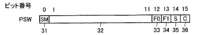
【0048】
図2は、PSW18の詳細を説明するための図である。このPSW18は、割込み用スタックポインタSPI16およびユーザ用スタックポインタSPU17のいずれを選択するかを示すスタックモード(SM)ビット31と、比較命令などでセットされ、条件分岐命令などの条件として参照される条件フラグであるF0フラグ33、F1フラグ34、サチュレーション(S)フラグ35およびキャリー(C)フラグ36とを含む。その他の状態フラグやモードビット32は、本発明と直接関係がないため詳細な説明は省略する。
【0049】
図3は、本実施の形態におけるデータ処理装置の命令フォーマットを説明するための図である。本実施の形態におけるデータ処理装置は、2ウェイのVLIW(Very Long Instruction Word)命令セットを処理する。基本命令長は、32ビット固定であり、32ビット境界に整置されている。PC値は32ビットの命令ワードアドレスで管理される。
【0050】
図3に示すように、32ビットの命令コードは、命令のフォーマットを示す2ビットのフォーマット指定(FM)ビット51と、15ビットの左コンテナ52と、15ビットの右コンテナ53とによって構成される。左コンテナ52および右コンテナ53は、それぞれ15ビットのショートフォーマットのサブ命令を格納できる他、2つのコンテナで30ビットのロングフォーマットのサブ命令を格納することもできる。以下、簡単のために、ショートフォーマットのサブ命令をショート命令と呼び、ロングフォーマットのサブ命令をロング命令と呼ぶことにする。
【0051】
図4は、FMビット51の内容を説明するための図である。FMビット51は、命令のフォーマットおよび2つのショート命令の実行順序を指定する。命令実行順序において、第1は先に実行される命令を示し、第2は後で実行される命令を示している。FMビット51が“11”の場合には、左コンテナ52および右コンテナ53が30ビットの1つのロング命令を保持することを示している。それ以外の場合には、左コンテナ52および右コンテナ53が、それぞれショート命令を保持することを示している。
【0052】
FMビット51が“00”の場合には、2つのショート命令を並列に実行することを示している。また、FMビット51が“01”の場合には、左コンテナ52に保持されるショート命令を実行した後、右コンテナ53に保持されるショート命令を実行することを示している。また、FMビット51が“10”の場合には、右コンテナ53に保持されるショート命令を実行した後、左コンテナ52に保持されるショート命令を実行することを示している。このように、シーケンシャルに実行される2つのショート命令を1つの32ビット命令にエンコードできるようにして、コード効率の向上を図っている。
【0053】
図5〜図7は、本実施の形態におけるデータ処理装置の典型的な命令のビット割付けの一例を示す図である。図5は、2つのオペランドを持ったショート命令のビット割付けを示している。フィールド61および64は、オペレーションコードフィールドである。また、フィールド64によって、アキュムレータ番号を指定する場合もある。
【0054】
フィールド62および63は、オペランドとして参照または更新されるデータの格納位置を、レジスタ番号やアキュムレータ番号で指定する。また、フィールド63によって、4ビットの即値を指定する場合もある。
【0055】
図6は、ショートフォーマットの分岐命令のビット割付けを示している。この命令フォーマットは、7ビットのオペレーションコードフィールド71と、8ビットの分岐変位フィールド72とによって構成される。分岐変位は、PC値と同様に、当該命令ワード(32ビット)からのオフセットで指定される。
【0056】
図7は、16ビットの変位や即値を持った3オペンランド命令やロード/ストア命令のビット割付けを示している。この命令フォーマットは、オペレーションコードフィールド81と、ショートフォーマットと同様にレジスタ番号などを指定するフィールド82および83と、16ビットの変位や即値などを指定する拡張データフィールド84とによって構成される。
【0057】
上述した命令フォーマット以外に、NOP(No OPeration)命令のように、15ビット全てがオペレーションコードとなる命令や、1オペランド命令などの特殊なビット割付けを有する命令もある。
【0058】
本実施の形態におけるデータ処理装置に実装される各サブ命令は、RISC(Reduced Instruction Set Computer)ライクな命令セットとなっている。メモリにアクセスする命令はロード/ストア命令のみである。演算命令は、レジスタまたはアキュムレータに格納されたオペランドや、即値オペランドに対する演算を行なう。
【0059】
オペランドデータに対するアクセスのアドレッシングモードとしては、レジスタ間接モード、ポストインクリメント付きレジスタ間接モード、ポストデクリメント付きレジスタ間接モード、プッシュモードおよびレジスタ相対間接モードの5種類がある。これら5種類のニーモニックはそれぞれ、“@Rsrc”、“@Rsrc+”、“@Rsrc−”、“@−SP”および“@(disp16,Rsrc)”で示される。Rsrcはベースアドレスを指定するレジスタ番号を示し、disp16は16ビットの変位値を示している。なお、オペランドのアドレスはバイトアドレスで指定される。
【0060】
レジスタ相対間接モード以外のロード/ストア命令は、図5に示す命令フォーマットとなる。すなわち、フィールド63によってベースレジスタ番号が指定され、フィールド62によってメモリからロードした値を書込むレジスタの番号またはストアする値を保持するレジスタの番号が指定される。
【0061】
レジスタ間接モードにおいては、ベースレジスタとして指定されたレジスタの値がオペランドアドレスとなる。
【0062】
ポストインクリメント付きレジスタ間接モードにおいては、ベースレジスタとして指定されたレジスタの値がオペランドアドレスとなり、このベースレジスタの値がオペランドのサイズ(バイト数)分だけポストインクリメントされてレジスタに書き戻される。
【0063】
ポストデクリメント付きレジスタ間接モードにおいては、ベースレジスタとして指定されたレジスタの値がオペランドアドレスとなり、このベースレジスタの値がオペランドのサイズ(バイト数)分だけポストデクリメントされてレジスタに書き戻される。
【0064】
プッシュモードは、ストア命令であり、かつベースレジスタがR15(SP)の場合にのみ使用可能であり、SP値がオペランドのサイズ(バイト数)だけポストデクリメントされてオペランドアドレスとなり、そのデクリメントされた値がSPに書き戻される。
【0065】
レジスタ相対間接モードのロード/ストア命令のフォーマットは、図7に示す命令フォーマットとなる。フィールド83によってベースレジスタの番号が指定され、フィールド82によってメモリからロードした値を書込むレジスタの番号またはメモリにストアする値を保持するレジスタの番号が指定される。また、フィールド84によってベースアドレスからの変位値が指定される。このレジスタ相対間接モードにおいては、ベースレジスタとして指定されたレジスタの値に16ビットの変位値が加算されて、オペランドアドレスとされる。
【0066】
ジャンプ命令のジャンプ先アドレス指定には、ジャンプ先アドレスをレジスタに格納された値で指定するレジスタ間接モードと、PC値からの分岐変位でジャンプ先アドレスを指定するPC相対間接モードとがある。このPC相対間接モードにおいては、分岐変位を8ビットで指定するショートフォーマットと、分岐変位を16ビットで指定するロングフォーマットとの2種類がある。
【0067】
図8は、本発明の第1の実施の形態におけるデータ処理装置の概略構成を示すブロック図である。このデータ処理装置100は、MPU(Micro Processing Unit)コア部101と、MPUコア部101からの要求に応じて命令データをフェッチする命令フェッチ部102と、内蔵命令メモリ103と、MPUコア部101からの要求に応じてオペランドデータのアクセスを行なうオペランドアクセス部104と、内蔵データメモリ105と、命令フェッチ部102およびオペランドアクセス部104からの要求を調停し、データ処理装置100の外部にあるメモリ対してアクセスを行なう外部バスインタフェース部106とを含む。
【0068】
また、MPUコア部101は、MPUコア部101の全体的な制御を行なう制御部111と、レジスタファイル115と、第1演算部116と、第2演算部117と、PC値を制御するPC部118とを含む。さらには、制御部111は、命令キュー112と、命令デコード部113とを含む。
【0069】
命令キュー112は、2エントリの32ビット命令バッファ、その有効ビットおよび入出力ポインタなどによって構成され、FIFO(First In First Out)方式で制御される。命令キュー112は、命令フェッチ部102によってフェッチされた命令データを一時保持し、この命令データを命令デコード部113へ送出する。命令デコード部113は、実行する命令データをデコードし、命令の実行に必要な制御信号を生成する。
【0070】
図9は、命令デコード部113をさらに詳細に説明するためのブロック図である。図9に示すブロック図は、本実施の形態におけるデータ処理装置の説明に必要な接続関係のみを示しており、その説明に関係しない部分については図示していない。
【0071】
この命令デコード部113は、命令キュー112から受けた命令データを保持する命令レジスタ121と、第1デコーダ122と、第2デコーダ123と、プリデコーダ124と、拡張データ生成部125と、Dステージ制御部126とを含む。
【0072】
命令レジスタ121は、命令キュー112から受けたデコード対象の命令データを保持する。なお、この命令レジスタ121に保持される命令データのフォーマットは、図3に示す命令フォーマットと同様である。
【0073】
命令デコード部113は、実行制御信号等を生成する2つのデコーダ(第1デコーダ122、第2デコーダ123)を備えており、2つのショート命令を並列にデコードすることが可能である。
【0074】
第1デコーダ122は、第1演算部116が実行する命令をデコードするものであり、主として第1演算部116、PC部118およびレジスタファイル115の命令実行制御信号や、分岐/ジャンプ/オペランドアクセスに関連した制御信号などを生成する。
【0075】
第2デコーダ123は、第2演算部117が実行する命令をデコードするものであり、主として第2演算部117およびレジスタファイル115の命令実行制御信号を生成する。
【0076】
プリデコーダ124は、2つのショート命令がシーケンシャルに実行される場合、先行して実行されるショート命令の実行中に後で実行するショート命令をデコードして、先行命令の実行後に第1デコーダ122および第2デコーダ123のどちらで後続命令のデコードを行なうかを判定する。
【0077】
なお、第1デコーダ122、第2デコーダ123およびプリデコーダ124は、それぞれマルチプレクサ(MUX)を有しており、左コンテナ52に保持されるショート命令と右コンテナ53に保持されるショート命令とのいずれかを選択的に入力することが可能である。
【0078】
拡張データ生成部125は、第1デコーダ122からデコード結果を受け、第1演算部116における命令実行に必要な即値、変位等の拡張データを切出す。ロングフォーマット命令の拡張データの切出しを行なうために、右コンテナ53に格納されるデータも拡張データ生成部125へ転送される。なお、第2演算部117における命令実行に必要な即値、変位等を生成する部分は、第2デコーダ123に含めて図示している。
【0079】
Dステージ制御部126は、後述する命令デコードステージ(Dステージ)における命令デコードの状態制御を行なう。なお、Dステージ制御部126は、命令デコード部113に含める必要はないが、命令の解析が関係するので、本実施の形態においては命令デコード部113に含めて説明するものとする。
【0080】
32ビット命令のデコードの第1サイクルにおいては、必ず左コンテナ52に格納される命令コードが第1デコーダ122において解析され、右コンテナ53に格納される命令コードが第2デコーダ123において解析される。ただし、FMビット51と左コンテナ52のビット0およびビット1とは、両方のデコーダによって解析される。したがって、最初に実行される命令は、その命令を実行する演算部に対応する位置に置かれなければならない。
【0081】
2つのショート命令がシーケンシャルに実行される場合には、プリデコーダ124におけるデコード結果にしたがって、先行するショート命令がデコードされた後、後で実行されるショート命令がデコードするべきデコーダに取込まれ、解析される。後で実行されるショート命令が、どちらのデコーダによっても処理できる命令の場合には、第1デコーダ122がそのショート命令をデコードする。
【0082】
レジスタファイル115は、図1に示す汎用レジスタR0〜R15(1〜17)に相当し、処理対象となるアドレス値やデータを保持する。このレジスタファイル115は、第1演算部116、第2演算部117、PC部118およびオペランドアクセス部104と複数のバスで接続されている。ワード/2ワードロード命令実行時には、ロードデータがオペランドアクセス部104から直接レジスタファイル115に取込まれる。
【0083】
第1演算部116は、主としてロード/ストア命令、分岐命令、算術演算命令、論理演算命令、比較命令、転送命令などを実行する。この第1演算部116は、レジスタファイル115、PC部118およびオペランドアクセス部104と複数のバスで接続されており、それらとの間で命令の実行に必要なデータやアドレスの転送を行なう。また、第1演算部116は、演算に必要な即値、変位等の拡張データを拡張データ生成部125から取込む。
【0084】
また、第1演算部116は、図示しないALU(Arithmetic and Logic Unit)を備えており、転送、比較、算術演算、論理演算、オペランドアドレスの計算/転送、オペランドアドレス値のインクリメント/デクリメント、ジャンプ先アドレスの計算/転送などを行なう。第1演算部116は、演算結果やアドレス更新結果をバスを介して、命令で指定されたレジスタファイル115内のレジスタに書き戻す。
【0085】
ロード/ストア命令実行時には、第1演算部116は、計算したオペランドアドレスをオペランドアクセス部104へ出力する。また、ジャンプ/分岐命令実行時には、ジャンプ先アドレスをPC部118へ出力する。
【0086】
ストア命令実行時には、第1演算部116は、レジスタファイル115から読出したストアデータを保持/整置した後、オペランドアクセス部104へ出力する。また、バイトロード時には、第1演算部116は、オペランドアクセス部104から取込んだロードデータのバイト整置およびゼロ/符号拡張を行ない、レジスタファイル115へ出力する。
【0087】
PC部118は、インクリメンタ等の演算器やラッチなどを備えており、制御部111の制御によって、命令のパイプライン処理に同期して命令フェッチアドレスの管理/更新、実行命令PC値の管理/更新を行なう。リセット直後を含め命令の処理シーケンスが切替わった場合に、PC部118はジャンプ先アドレスを第1演算部116から取込み、PC部118内の種々のアドレスラッチの値が初期設定される。
【0088】
命令フェッチ時には、PC部118は、次にフェッチする命令のアドレスを命令フェッチ部102へ出力する。また、分岐命令の処理時には、PC部118は、分岐先アドレスの計算に必要な分岐命令のアドレスを第1演算部116へ出力する。また、サブルーチンジャンプ/分岐命令の場合には、PC部118は、サブルーチンジャンプ/分岐命令の次命令アドレスを戻り先アドレスとしてレジスタファイル115へ出力する。
【0089】
第2演算部117は、主として積和演算を含む算術演算、シフト処理、ビット操作、比較、転送などの処理を行なう。第2演算部117は、レジスタファイル115と複数のバスで接続されており、参照オペランドデータをレジスタファイル115から読出し、書込みオペランドデータをレジスタファイル115へ出力する。
【0090】
第2演算部117は、40ビットALU、40ビットバレルシフタ、17ビット×17ビット乗算器、プライオリティエンコーダなどの演算器と、図1に示す2本の40ビットアキュムレータ31および32とを含む。
【0091】
図10は、本発明の第1の実施の形態におけるデータ処理装置100のパイプライン処理を説明するための図である。データ処理装置100は、命令データのフェッチを行なう命令フェッチ(IF)ステージ401と、命令の解析を行なう命令デコード(D)ステージ402と、演算実行を行なう命令実行(E)ステージ403と、データメモリに対するアクセスを行なうメモリアクセス(M)ステージ404と、メモリからロードしたバイトオペランドをレジスタに書込むライトバック(W)ステージ405との5段のパイプライン処理を行なう。
【0092】
Eステージ403における演算結果のレジスタへの書込みは、Eステージ403で完了する。また、ワード(2バイト)、2ワード(4バイト)ロード時におけるレジスタへのデータ書込みは、Mステージ404で完了する。積和/積差演算については、さらに乗算と加算との2段のパイプラインで命令の実行が行なわれる。この後段の処理(加算)を命令実行2(E2)ステージ406と呼ぶ。このように、2段のパイプラインで乗算と加算とを行なうことにより、連続する積和/積差演算を1回/1クロックサイクルのスループットで実行できる。
【0093】
IFステージ401においては、主として命令のフェッチおよび命令キュー112の管理が行なわれる。命令フェッチ部102、内蔵命令メモリ103、外部バスインタフェース部106およびPC部118の命令フェッチアドレス管理に関する部分や、制御部111のIFステージ制御、命令フェッチ制御、PC部118の制御などを行なう部分が、このIFステージ401の制御で動作する。IFステージ401は、Eステージ403におけるジャンプの実行時に初期化される。
【0094】
IFステージ401においては、命令キュー112に空きがある場合、制御部111が命令フェッチ要求を命令フェッチ部102へ出力する。命令フェッチ部102は、PC部118から転送された命令フェッチアドレスの値に応じて、命令データのフェッチを行なう。
【0095】
対応する命令データが内蔵命令メモリ103にある場合には、命令フェッチ部102は内蔵命令メモリ103から命令データをフェッチする。この場合、1クロックサイクルで32ビットの命令データのフェッチが完了する。
【0096】
対応する命令データが内蔵命令メモリ103にない場合には、命令フェッチ部102は外部バスインタフェース部106に命令フェッチ要求を出力する。外部バスインタフェース部106は、この命令フェッチ要求とオペランドアクセス部104からの要求との調停を行ない、命令のフェッチが可能となったときに外部メモリから命令データを取込み、命令フェッチ部102へ出力する。外部バスインタフェース部106は、最小2クロックサイクルで外部メモリに対するアクセスを行なうことが可能である。命令フェッチ部102は、フェッチした命令を命令キュー112へ出力する。命令キュー112に取込まれた命令データが、順次命令デコード部113へ出力される。
【0097】
Dステージ402においては、命令デコード部113がオペレーションコードの解析を行ない、第1演算部116、第2演算部117、PC部118などの命令の実行に関連した部分を制御するための制御信号群を生成する。Dステージ402は、Eステージ403におけるジャンプの実行時に初期化される。Dステージ402において、命令キュー112から無効な命令コードが転送された場合には、アイドルサイクルとなって有効な命令コードが転送されるまで待機する。
【0098】
Eステージ403が次の処理を開始できない場合には、命令デコーダ113は演算器などに出力する制御信号を無効化し、Eステージ403における先行命令の処理の終了を待つ。たとえば、Eステージ403で実行中の命令がメモリアクセスを行なう命令であり、そのときMステージ404でメモリアクセスを行なっている場合には、Eステージ403における先行命令の処理が待たされて、このような状態になる。
【0099】
また、Dステージ402においては、シーケンシャルに実行が行なわれる2命令の分割や、2サイクル実行命令のシーケンス制御も行なわれる。さらに、Dステージ402において、図示しないスコアボードレジスタを用いたロードオペランドの干渉チェックや、第2演算部117の演算器の干渉チェックなども行なわれ、干渉が検出された場合には、干渉が解消されるまで処理の発行を抑止する。
【0100】
ワードまたは2ワードのロード命令の直後に、ロードするオペランドを参照する演算命令がある場合には、レジスタへのロードが完了するまで演算命令の実行開始を抑止する。この場合、メモリアクセスが1クロックサイクルで終了する場合でも、1クロックサイクルのストールが発生する。バイトデータをロードする場合には、さらにWステージ405でレジスタファイル115への書込みが完了するため、さらに1サイクルだけストール期間が延びる。
【0101】
また、積和演算命令の直後に加算器を使用する丸め処理がある場合には、命令デコード部113は、先行の積和演算命令の演算が終了するまで丸め命令の実行開始を抑止する。この場合、1クロックサイクルのストールが発生する。積和演算命令が連続する場合には、ストールは発生しない。
【0102】
Eステージ403においては、演算、比較、制御レジスタを含むレジスタ間転送、ロード/ストア命令のオペランドアドレス計算、ジャンプ命令のジャンプ先アドレスの計算、ジャンプ処理、EIT(例外、割込み、トラップ)検出、各EITのベクタアドレスへのジャンプなど、メモリアクセスと積和/積差演算命令の加減算処理とを除く命令処理に関するほとんど全ての処理が行なわれる。
【0103】
Eステージ403は、Dステージ402から処理が発行されないと、アイドル状態となる。Eステージ403で処理中の命令がオペランドアクセスを行なう命令であり、Mステージ404でメモリアクセスが完了していない場合には、Eステージ403における処理の完了が待たされる。
【0104】
Eステージ403において、第1演算部116は、算術演算、論理演算、比較、転送、メモリオペランドのアドレスや分岐先のアドレス計算などを行なう。Eステージ403において、レジスタファイル115内の汎用レジスタ、第1演算部116やPC部118内の制御レジスタ、命令デコード部113から取込まれた即値、変位などの拡張データの値がソースオペランドとして読出される。
【0105】
演算命令の実行時には、第1演算部116内のALUにおいて転送を含む演算が行なわれる。デスティネーションオペランドが汎用レジスタや制御レジスタの場合には、ALUにおける演算結果がレジスタファイル115、若しくは、第1演算部116またはPC部118内の制御レジスタに書込まれる。
【0106】
ロード/ストア命令の場合には、第1演算部116が演算結果(アドレス値)をオペランドアクセス部104へ転送する。ジャンプ命令の場合には、第1演算部116がジャンプ先アドレスをPC部118へ転送する。また、ストア命令の場合には、第1演算部116がレジスタファイル115から読出したストアデータを整置し、その値を保持する。
【0107】
また、Eステージ403においては、実行する命令に依存しないPC値の更新も行なわれる。PC部118は、実行中の命令のPC値の管理や、次に実行する命令のアドレスの生成を行なう。Eステージ403において、ジャンプが起こった場合には、第1演算部116がジャンプ先アドレスをPC部118へ転送し、初期化が行なわれる。シーケンシャルにショート命令の実行が行なわれる場合には、32ビット命令の処理が開始されるたびに、PC部118内の図示しないインクリメンタがPC値を1だけインクリメントする。
【0108】
Eステージ403において、第2演算部117は、算術演算、論理演算、比較、転送、シフトなど、積和演算の加算以外の全ての演算処理を行なう。第2演算部117は、オペランドの値として、レジスタファイル115やアキュムレータに保持される値、第2デコーダ123によって切出された即値を読出し、第2演算部117内の演算器でその値に指定された演算を行なう。そして、演算結果がレジスタファイル115またはアキュムレータに書込まれる。
【0109】
Eステージ403においては、第1演算部116または第2演算部117における演算結果によるPSW中のフラグ値の更新制御も行なわれる。また、Eステージ403は、第2デコーダ123が生成した積和/積差演算における加算/減算の実行のための演算制御信号を保持する。メモリアクセス情報、ロードレジスタ情報は、Mステージ404に転送される。なお、Eステージ403のステージ制御は制御部111によって行なわれる。
【0110】
Mステージ404は、制御部111からのオペランドアクセス要求に応じて、第1演算部116から転送されたアドレスを用いてオペランドのアクセスを行なう。オペランドアクセス部104は、オペランドが内蔵データメモリ105や図示しないチップ内I/Oにある場合には、内蔵データメモリ105やチップ内I/Oに対して、1クロックサイクルで1回のオペランドの読出し、または書込みを行なう。
【0111】
オペランドが内蔵データメモリ105やチップ内I/Oにない場合には、外部バスインタフェース106に対してデータアクセス要求を出力する。外部バスインタフェース部106は、データアクセス要求を受けると、外部メモリに対してデータアクセスを行なう。
【0112】
ロードの場合には、オペランドアクセス部104は、外部バスインタフェース部106によって読出されたデータをバスを介して転送する。バイトデータの場合には、第1演算部116へデータが転送される。また、ワードまたは2ワードデータの場合には、レジスタファイル115に直接データが書込まれる。
【0113】
ストアの場合には、オペランドアクセス部104が第1演算部116から整置されたストアデータを受け、外部バスインタフェース部106を介して、対象となる外部メモリにデータを書込む。非整置アクセス時における後半アクセスのアドレス生成およびアクセス制御は、Mステージ404において行なわれる。
【0114】
バイトデータのロードの場合には、Wステージ405において、第1演算部116内に保持されたロードオペランド(バイト)が、整置、ゼロ/符号拡張された後、レジスタファイル115に書込まれる。
【0115】
E2ステージ406においては、積和/積差演算の加算処理または減算処理が行なわれ、加算結果または減算結果がアキュムレータに書き戻される。
【0116】
本実施の形態におけるデータ処理装置は、入力クロックに基づいて内部制御を行ない、最短の場合、各パイプラインステージは1クロックサイクルで処理を終了する。なお、本実施の形態においては、クロック制御が直接関係しないので、詳細な説明は省略する。
【0117】
次に、各サブ命令の処理の一例について説明する。加算/減算、論理演算、比較などの演算命令やレジスタ間の転送命令は、IFステージ401、Dステージ402およびEステージ403の3段で処理が終了する。演算やデータ転送は、Eステージ403で行なわれる。
【0118】
積和/積差演算命令は、Eステージ403における乗算処理と、E2ステージ406における加算/減算処理との2クロックサイクルで演算実行される。したがって、IFステージ401、Dステージ402、Eステージ403およびE2ステージ406の4段で処理が終了する。
【0119】
バイトロード命令は、IFステージ401、Dステージ402、Eステージ403、Mステージ404およびWステージ405の5段で処理が終了する。ワード/2ワードロード命令やストア命令は、IFステージ401、Dステージ402、Eステージ403およびMステージ404の4段で処理が終了する。
【0120】
非整置アクセスの場合には、Mステージ404においては、オペランドアクセス部104が2回のアクセスに分割して、メモリアクセスを行なう。Eステージ403においては、1クロックサイクルで処理が終了する。実行に2サイクルを要する命令においては、第1命令デコーダ122または第2命令デコーダ123が各サイクル毎に実行制御信号を生成して出力し、第1演算部116または第2演算部117が2サイクルで演算実行を行なう。
【0121】
ロング命令は、上述したように、1つの32ビット命令が1つのロング命令で構成されているが、この1つのロング命令の処理によって32ビット命令の実行が完了する。
【0122】
2つのショート命令がパラレルで実行される場合には、2つのショート命令のうち処理サイクルの大きい方の命令の処理に律速される。たとえば、2サイクルで実行する命令と、1サイクルで実行する命令との組合わせの場合、この2つのショート命令の実行に2サイクルを要する。
【0123】
2つのショート命令がシーケンシャルに実行される場合には、各サブ命令の組合せによって処理サイクルが決定される。すなわち、デコード段階で各命令がシーケンシャルにデコードされ、各命令がシーケンシャルに実行される。たとえば、Eステージ403において1サイクルで実行が完了する2つの加算命令の場合、Dステージ402とEステージ403とのそれぞれが各命令に1サイクル、計2サイクルで処理を終了する。Eステージ403における先行命令の実行と並列に、Dステージ402における後続命令のデコードが行なわれる。
【0124】
次に、本発明の第1の実施の形態におけるデータ処理装置が実行するオペレーション修飾命令について詳細に説明する。図11〜図14は、オペレーション修飾命令のビット割付けを説明するための図である。
【0125】
図11に示すMOD_SAT命令は、並列実行においてのみ使用可能な命令であり、並列に実行する他方の命令のオペレーションについて、16ビットのサチュレーションを行なうことを指示する命令である。
【0126】
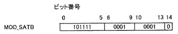
図12に示すMOD_SATB命令は、図11に示すMOD_SAT命令と同様に、並列実行においてのみ使用可能な命令であり、並列に実行する他方の命令のオペレーションについて、8ビットのサチュレーションを行なうことを指示する命令である。
【0127】
図13に示すMOD_SATN命令は、次命令のオペレーションについて、サチュレーションを行なうことを指示する命令である。ロングフォーマットのサブ命令や、並列実行する2つのショートフォーマットのサブ命令についてサチュレーションを行なう場合に使用される。
【0128】
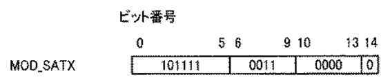
図14に示すMOD_SATX命令は、並列に実行する他方の命令と次命令とのオペレーションについて、サチュレーションを行なうことを指示する命令である。
【0129】
これらのオペレーション修飾命令は、自身では処理を行なわないNOP命令である。また、オペレーション修飾命令は、左コンテナ52および右コンテナ53のいずれにも配置可能である。
【0130】
図15は、レジスタ間の16ビット加算を行なうADD命令のビット割付けを説明するための図である。このADD命令が実行されると、Rdestによって指定されるレジスタの値に、Rsrcによって指定されるレジスタの値が加算され、加算結果がRdestによって指定されるレジスタに書き戻される。この加算命令は単独で実行可能である。この場合には、サチュレーションは行なわれない。
【0131】
図16は、2つのADD命令を並列に実行する場合の32ビット命令を示す図である。第1演算部116によって“ADD R0,R2”が実行され、第2演算部117によって“ADD R1,R3”が実行される。この32ビット命令が単独で実行される場合には、サチュレーションは行なわれない。
【0132】
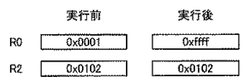
図17および図18は、“ADD R0,R2”が単独で実行された場合の演算の前後のレジスタ値およびサチュレーション(S)フラグの値を示す図である。なお、“0x”はそれ以下が16進数で表記されていることを示している。図17においては、符号付き16ビット数を加算する場合であって、オーバーフローが発生する例を示している。しかし、サチュレーション処理は行なわれず、16ビットとして加算した演算結果がそのままレジスタR0に書込まれる。このとき、Sフラグは変化しない。
【0133】
図18においては、符号付き16ビット数を加算する場合であって、アンダーフローが発生する例を示している。この場合もサチュレーション処理は行なわれず、16ビットとして加算した演算結果がそのままレジスタR0に書込まれる。このときも、Sフラグは変化しない。
【0134】
図19は、ADD命令がMOD_SAT命令と並列に実行される場合の32ビット命令を示す図である。左コンテナ52にMOD_SAT命令が配置され、右コンテナ53にADD命令が配置されている。命令デコード部113は、2つの命令を並列にデコードする。第1デコーダ122は、MOD_SAT命令をデコードし、実行制御情報として有効な処理を行なわないノーオペレーション情報を生成して、第1演算部116などへ出力する。第1デコーダ122は、第2デコーダ123に対して、第2デコーダ123がデコード中の命令に対して16ビットのサチュレーションを行なうよう演算内容を修飾することを指示する情報を、信号線127を介して第2デコーダ123へ出力する。
【0135】
第2デコーダ123は、ADD命令をデコードし、加算処理を行なうための演算制御情報を生成し、レジスタファイル115および第2演算部117に出力する。このとき、信号線127によって、16ビットのサチュレーションを行なうよう演算内容を修飾することが指示されていれば、第2デコーダ123はサチュレーションを行なうための制御信号を生成して第2演算部117などに出力する。
【0136】
図20は、第2演算部117内のALU、シフタおよびその周辺回路の構成を示すブロック図である。なお、第2演算部117は、他の多くの演算器を備えているが、本発明と直接関係しない部分については省略している。
【0137】
第2演算部117は、ALU演算用のラッチA131およびB132と、ALU133と、ALU演算用オーバーフロー判定回路134と、ALU133の出力を選択するセレクタ135と、シフト量入力ラッチSC141と、シフトデータ入力ラッチSD142と、シフタ143と、シフト演算用オーバーフロー判定回路144と、シフタ143の出力を選択するセレクタ145と、即値部(IMM)151とを含む。
【0138】
即値部151は、命令コードから切出された即値を取込み、即値を符号/ゼロ拡張したり、ビット演算用ビットマスクデータを作成したりする。
【0139】
次に、図19に示す命令が実行される場合の第2演算部117の動作について、図20を参照しながら説明する。左コンテナ52にMOD_SAT命令があるので、第1演算部116は有効な演算を行なわない。第2演算部117は、サチュレーションを伴う加算処理を行なう。
【0140】
まず、レジスタR0およびR2の値がレジスタファイル115から読出され、それぞれラッチA131およびB132に転送される。ALU133は、ラッチA131およびB132に保持される値に対して加算処理を行なう。サチュレーション制御信号136によって、16ビットのサチュレーションを行なうことが指示されているので、判定回路134はALU133の演算結果(ビット0およびビット1のキャリー出力情報など)に基づき、オーバーフローまたはアンダーフローの判定を行ない、その判定結果をセレクタ135の選択信号として出力する。
【0141】
オーバーフローが検出された場合には、セレクタ135は、正の最大値“0x7fff”を出力する。また、アンダーフローが検出された場合には、セレクタ135は、負の最小値“0x8000”を出力する。また、オーバーフローもアンダーフローも検出されなかった場合には、セレクタ135は、ALU133の出力を選択して出力する。このセレクタ135の出力は、レジスタR0に書き戻される。
【0142】
また、オーバーフローまたはアンダーフローが検出された場合には、制御部111内のSフラグ35が“1”にセットされる。オーバーフローもアンダーフローも検出されなかった場合には、制御部111内のSフラグ35がゼロクリアされる。第2の演算部117から制御部111への演算結果の出力やフラグ制御の詳細は、本発明の説明に必要ないので説明を省略する。
【0143】
図21および図22は、オペレーションが修飾された命令“ADD R0,R2”が実行された場合の演算の前後のレジスタ値およびSフラグの値を示す図である。図21においては、符号付き16ビット数を加算する場合であって、オーバーフローが発生する例を示している。サチュレーション処理が行なわれるので、演算実行後のレジスタR0には正の最大値“0x7fff”が書込まれる。このとき、オーバーフローが発生するので、Sフラグは“1”となる。
【0144】
図22においては、符号付き16ビット数を加算する場合であって、アンダーフローが発生する例を示している。この場合もサチュレーション処理が行なわれるので、演算後のレジスタR0には負の最小値“0x8000”が書込まれる。このとき、アンダーフローが発生するので、Sフラグは“1”となる。
【0145】
図16に示すようなオペレーションが修飾されないADD命令が実行される場合には、第2デコーダ123は、信号線127によってオペレーション修飾を行なわないことを示す情報を受け、サチュレーション制御信号136によってサチュレーションを行なわないことを指示する。この場合、オーバーフローまたはアンダーフローが発生したか否かに関係なく、セレクタ135がALU133の出力を選択する。この加算結果がレジスタファイル115に書き戻される。また、制御部111内のSフラグ35は、このADD命令の実行の影響を受けない。
【0146】
次に、シフト命令についてオペレーション修飾が行なわれる場合の第2演算部117の動作について説明する。図23は、シフト量が4ビットの即値で指定される左シフト命令SLLIのビット割付けを説明するための図である。Rdestによって指定されるレジスタの値が、imm4によって指定されるシフト量分だけ左シフトされ、Rdestによって指定されるレジスタに書き戻される。
【0147】
オペレーション修飾を行なわない場合には、オーバーフローまたはアンダーフローが発生したか否かに関係なく、シフトした値がそのままレジスタに書き戻される。オペレーション修飾を行なう場合には、シフトアウトされたデータも含めてオーバーフローまたはアンダーフローの判定が行なわれ、サチュレーション処理が行なわれる。また、制御部111内のSフラグ35も演算の実行による影響を受ける。
【0148】
図24は、SLLI命令がMOD_SAT命令と並列に実行される場合の32ビット命令を示す図である。左コンテナ52にMOD_SAT命令が配置され、右コンテナ53にSLLI命令が配置されている。命令のデコード方法は、実行される命令が加算命令ではなく、シフト命令であることを除き、図19を用いて説明した方法と同様である。
【0149】
次に、図24に示す命令が実行される場合の第2演算部117の動作について、図20を参照しながら説明する。左コンテナ52にMOD_SAT命令があるので、第1演算部116は有効な演算を行なわない。第2演算部117は、サチュレーションを伴う左シフト処理を行なう。
【0150】
まず、レジスタR0の値がレジスタファイル115から読出され、ラッチSD142に転送される。また、命令コードから切出された即値がIMM151によってゼロ拡張され、ラッチSC141に転送される。シフタ143は、ラッチSC141およびSD142に保持される値を参照して左シフト処理を行ない、シフト結果をセレクタ145へ出力する。
【0151】
サチュレーション制御信号146によって、サチュレーションを行なうことが指示されているので、判定回路144はシフタ143に入力される値に基づき、オーバーフローまたはアンダーフローの判定を行ない、その判定結果をセレクタ145の選択信号として出力する。判定回路144は、ラッチSC141に保持されるシフト量に基づいて、ラッチSD142に保持される値(シフトデータ)のMSB側の2ビット目から、LSB側へシフト量分だけ“1”になっているマスクデータを生成する。
【0152】
そして、シフトデータのMSB側の2ビット目からLSBまでの各ビットと、符号ビット(MSBの値)との排他的論理和を演算し、この演算結果の各ビット毎にマスクデータとの論理積を演算する。その結果、いずれかのビットが“1”であり、かつシフトデータの符号が正(MSBが“0”)であれば、オーバーフローが発生したと判定する。また、いずれかのビットが“1”であり、かつシフトデータの符号が負(MSBが“1”)であれば、アンダーフローが発生したと判定する。
【0153】
オーバーフローが検出された場合には、セレクタ145は、正の最大値“0x7fff”を出力する。また、アンダーフローが検出された場合には、セレクタ145は、負の最小値“0x8000”を出力する。また、オーバーフローもアンダーフローも検出されなかった場合には、セレクタ145は、シフタ143の出力を選択して出力する。このセレクタ145の出力は、レジスタR0に書き戻される。
【0154】
また、オーバーフローまたはアンダーフローが検出された場合には、制御部111内のSフラグ35が“1”にセットされる。オーバーフローもアンダーフローも検出されなかった場合には、制御部111内のSフラグ35がゼロクリアされる。
【0155】
次に、右コンテナ53にオペレーション修飾命令がある場合の動作について説明する。図25は、ADD命令が左コンテナ52に配置され、MOD_SAT命令が右コンテナ53に配置される場合の32ビット命令を示す図である。命令デコード部113は、2つの命令を並列にデコードする。第2デコーダ123は、MOD_SAT命令をデコードし、実行制御情報として有効な処理を行なわないノーオペレーション情報を生成して、第2演算部117などへ出力する。第2デコーダ123は、第1デコーダ122に対して、第1デコーダ122がデコード中の命令に対して16ビットのサチュレーションを行なうよう演算内容を修飾することを指示する情報を、信号線128を介して第1デコーダ122へ出力する。
【0156】
第1デコーダ122は、ADD命令をデコードし、加算処理を行なうための演算制御情報を生成し、レジスタファイル115および第1演算部116に出力する。このとき、信号線128によって、サチュレーションを行なうよう演算内容を修飾することが指示されていれば、第1デコーダ122はサチュレーションを行なうための制御信号を生成して第1演算部116などに出力する。
【0157】
図26は、第1演算部116内のALU、整置回路およびその周辺回路の構成を示すブロック図である。なお、第1演算部116は、他の多くの演算器を備えているが、本発明と直接関係しない部分については省略している。
【0158】
第1演算部116は、ALU演算用のラッチA161およびB162と、ALU163と、ALU演算用オーバーフロー判定回路164と、ALU163の出力を選択するセレクタ165と、アドレスを保持するラッチ166と、整置用のラッチ171、172および175と、サチュレーション(SAT)回路173と、整置回路174とを含む。
【0159】
ALU163およびその周辺回路161、162、164および165は、図20に示す第2演算部117内のALU133およびその周辺回路131、132、134および135と同様であるので、詳細な説明は繰返さない。なお、ラッチ166は、アドレスを保持して出力する。
【0160】
図25に示す命令が実行される場合、右コンテナ53にMOD_SAT命令があるので、第2演算部117は有効な演算を行なわない。第1演算部116は、サチュレーションを伴う加算処理を行なう。なお、図25に示す命令が実行される場合の動作は、図19に示す命令が実行される場合の動作と同様であるので、詳細な説明は繰返さない。
【0161】
図27は、レジスタ間接モードのバイトストア(STB)命令の命令ビット割付けを示す図である。このSTB命令が実行されると、Rsrc1で指定されるレジスタの値の下位8ビットが、Rsrc2で指定されるレジスタの値が示すアドレスにストアされる。
【0162】
図28は、STB命令がMOD_SATB命令と並列に実行される場合の32ビット命令を示す図である。左コンテナ52にSTB命令が配置され、右コンテナ53にMOD_SATB命令が配置されている。命令デコード部113は、2つの命令を並列にデコードする。第2デコーダ123は、MOD_SATB命令をデコードし、実行制御情報として有効な処理を行なわないノーオペレーション情報を生成して、第2演算部117などへ出力する。第2デコーダ123は、第1デコーダ122に対して、第1デコーダ122がデコード中の命令に対して8ビットのサチュレーションを行なうよう演算内容を修飾することを指示する情報を、信号線128を介して第1デコーダ122へ出力する。
【0163】
次に、図28に示す命令が実行される場合の第1演算部116の動作について、図26を参照しながら説明する。右コンテナ53にMOD_SATB命令があるので、第2演算部117は有効な演算を行なわない。第1演算部116は、サチュレーションを伴うストア処理を行なう。
【0164】
まず、レジスタR0の値(ストアデータ)がレジスタファイル115から読出され、ラッチ171に転送される。サチュレーション制御信号176によって、8ビットのサチュレーションを行なうことが指示されているので、サチュレーション回路173は16ビットデータを入力とし、8ビットで表現できる値にサチュレーションを行なう。すなわち、“0x007f”以上の値は“0x007f”にクリッピングされ、“0xff80”以下の値は“0xff80”にクリッピングされて出力される。なお、サチュレーションを行なわない場合には、入力された値がそのまま出力される。
【0165】
整置回路174は、ラッチA161に保持されるアドレスに基づいて整置を行なう。この整置された値はラッチ175によって保持され、オペランドアクセス部104へ出力される。また、オペランドアドレスについては、レジスタファイル115内のレジスタR8の値がラッチA161に保持され、ラッチ166を介してオペランドアクセス部104へ出力される。オペランドアクセス部104は、ラッチ175に保持されるオペランドを、ラッチ166に保持されるオペランドアドレスにストアする。
【0166】
次に、左コンテナ52に保持されるレジスタ間転送命令“MV Rdest,Rsrc”と、右コンテナ53に保持されるMOD_SATB命令とが並列に実行される場合について説明する。MV命令を実行する場合、第1演算部116において、Rsrcで指定されたレジスタの値がラッチ171に転送される。サチュレーション回路173は、ラッチ171に保持される値に対してサチュレーションを行ない、レジスタファイル115内のRdestで指定されたレジスタにその値を書き戻す。このようにして、16ビットデータを8ビットデータにサチュレーションすることが可能である。
【0167】
次に、次命令のオペレーションを修飾するMOD_SATN命令の動作について説明する。図29は、即値の加算を行なう3オペランド加算(ADD3)命令の命令ビット割付けを示す図である。このADD3命令が実行されると、Rsrcで指定されるレジスタの値と、imm16で指定される16ビットの即値とが加算され、この加算結果がRdestで指定されるレジスタに書き戻される。
【0168】
このADD3命令は、ロングフォーマットの命令であるため、MOD_SAT命令を使用することができない。図30は、ロングフォーマットのADD命令のオペレーションを修飾する場合の一例を示す図である。図30に示すように、ADD3命令のオペレーションを修飾する場合、MOD_SATN命令の実行直後に、ADD3命令が実行される。
【0169】
MOD_SATN命令が右コンテナ53に格納されているため、MOD_SATN命令は第2デコーダ123でデコードされる。MOD_SATN命令自体は、有効なオペレーションを行なわないNOP命令である。第2デコーダ123がMOD_SATN命令をデコードすると、Dステージ制御部126に対して、次命令のオペレーションを修飾することを指示する情報を出力する。Dステージ制御部126は、この情報を次命令がデコードされるまで保持し、次命令デコード時にこの情報を第1デコーダ122および第2デコーダ123へ出力する。
【0170】
第1デコーダ122がADD3命令をデコードするが、このときDステージ制御部126から出力される次命令のオペレーションの修飾を指示する情報にしたがって、サチュレーションを伴うことを示す演算制御信号を生成し、第1演算部116へ出力する。第1演算部116は、この演算制御信号を受けて、サチュレーションを伴う加算処理を行なう。
【0171】
まず、レジスタファイル115内のレジスタR0の値がラッチA161に転送され、第1デコーダ122から出力された即値がラッチB162に転送される。ALU163は、ラッチA161およびB162に保持される値を加算し、サチュレーション処理を行なった後、その演算結果をセレクタ165を介してレジスタファイル115内のR0に書き戻す。
【0172】
次に、並列に実行する命令と次に実行する命令とのオペレーションを修飾するMOD_SATX命令について説明する。図31は、MOD_SATX命令の使用方法の一例を示す図である。このMOD_SATX命令がデコードされるときに、MOD_SAT命令とMOD_SATN命令との両方の処理が行なわれる。したがって、MOD_SATX命令と並列に実行される命令“ADD R8,R9”と、次に実行される命令“ADD R0,R2”および“ADD R1,R3”とがサチュレーションを伴って実行される。
【0173】
オペレーション修飾命令としてサチュレーションを行なう場合について説明した。画像処理ではバイトデータを扱う場合も多い。このため、本実施の形態におけるデータ処理装置では、2つのバイトデータに関するSIMD(Single Instruction Multiple Data stream)演算機能を備えている。以下、オペレーション修飾命令としてSIMD演算を行なう場合について説明する。
【0174】
図32は、並列に実行するペアの命令のオペレーションについて、8ビットの2つの演算を並列に行なうことを指示するMOD_2B命令であり、並列実行のみ可能な命令である。MOD_2B命令自身は、演算処理を行なわない(NOP)。MOD_2B命令は、左コンテナ52および右コンテナのいずれにも配置可能である。
【0175】
図33は、SUB命令が、MOD_2B命令と並列に実行される場合の一例を示す図である。“SUB R0,R2”命令は、R0の値からR2の値を減算し、R0に書戻す命令である。左コンテナ52にMOD_2B命令が、右コンテナ53にSUB命令が配置されており、図9に示した命令デコード部113において2つの命令が並列にデコードされる。MOD_2B命令は第1デコーダ122でデコードされ、第1演算部116に転送する実行制御情報として有効な処理を行なわないノーオペレーション情報を生成し、第1演算部116等に出力する。
【0176】
また、第1デコーダ122から、第2デコーダ123でデコード中の命令に対して、2つのバイトオペレーションを行なうように演算内容を修飾することを指示する情報が信号線127で第2デコーダ123に送られる。SUB命令は第2デコーダ123でデコードされ、減算処理を行なうための演算制御情報が生成され、レジスタファイル115および第2演算部117に出力される。このとき、信号線127で2つのバイトオペレーションを行なうよう演算内容を修飾することが指示されている場合には、2つのバイトオペレーションを行なうための制御信号が生成され、出力される。
【0177】
図34は、2つのバイトオペレーションのSIMD処理を説明するために、第2演算部117内のALU133周りのブロック構成を詳細に示した図である。上位8ビットと下位8ビットとが各々独立に算術演算できる機能を有している。図34において、図20と同一の構成および機能を有する部分には同一の参照符号が付けられている。なお、第2演算部117は、他の多くの制御信号が存在するが、本発明と直接関係しない部分については省略している。
【0178】
第2演算部117は、上位8ビットのALU用のラッチ131aおよび132aと、下位8ビットのALU用のラッチ131bおよび132bと、上位8ビットのALU部分であるALU_H133aと、下位8ビットのALU部分であるALU_L133bと、ALU_H133aへのキャリー入力を選択するセレクタ133cと、ALU演算用オーバーフロー判定回路134と、ALU_H133aおよびALU_L133bの出力を選択するセレクタ135とを含む。
【0179】
図33に示した命令が実行される場合の第2演算部117動作について、図34を参照しながら説明する。2つのバイトデータのSIMD演算を行なう場合、本実施の形態におけるデータ処理装置は1つの16ビットレジスタの上位8ビットと下位8ビットとに各々処理対象のバイトデータが格納されているものとして処理を行なう。
【0180】
第1演算部116は、左コンテナ52にMOD_2B命令があるので、第1演算部116は有効な演算を行なわない。第2演算部117は、2つのバイト(8ビット)減算処理を行なう。レジスタR0およびR2の値がそれぞれレジスタファイル115から読出され、上位8ビットが各々ラッチA_H131aおよびラッチB_H132aに転送され、下位8ビットが各々ラッチA_L131bおよびB_L132bに転送される。
【0181】
ALU_H133aおよびALU_L133bにおける減算処理は、キャリー入力CYIを“1”にし、ラッチA_H131aまたはA_L131bから取込まれた値に、ラッチB_H132aまたはB_L132bから取込まれた値の反転値を加えることによって実現される。図33に示す命令実行時において、第2デコーダ123は、キャリー入力138を“1”とし、キャリー選択信号137をセレクタ133cがキャリー入力138を選択する値にする。
【0182】
このように制御することによって、ALU_H133aにおいて上位8ビットの減算処理が行なわれ、ALU_L133bにおいて下位8ビットの減算処理が行なわれる。2つのバイト減算結果は連結され、セレクタ135を介してレジスタファイル115内のレジスタR0に書戻される。
【0183】
図35は、2つのバイトデータの減算処理の結果の一例を示す図である。上位8ビットの“0x00−0x01”と、下位8ビットの“0x01−0x02”とがそれぞれ計算され、その演算結果である“0xff”(上位8ビット)と“0xff”(下位8ビット)とが連結されて、レジスタR0に書戻される。
【0184】
“SUB R0,R2”命令が第2演算部117において単独で実行される場合についても簡単に説明しておく。この場合、16ビットの減算処理が行なわれる。命令デコード時に、信号127でオペレーション修飾を行なわない情報が第2デコーダ123に転送され、キャリー選択信号137でセレクタ133cがALU_L133bからのキャリー出力CYO139を選択する値がセレクタ139に転送される。その他の演算制御信号は、2つのバイトデータを演算する場合と同様である。このようにして、16ビットの減算処理が実現される。
【0185】
図36は、図35と同じ初期値で16ビットデータの減算処理を行なった場合の演算処理を説明するための図である。図35と異なり、演算結果として16ビットの演算結果である“0xfeff”がレジスタR0に書戻される。
【0186】
上述したオペレーション修飾命令として、サチュレーションを行なうMOD_SATN命令やMOD_SATX命令と同様に、本実施の形態におけるデータ処理装置は、次命令のオペレーションについて2つのバイトオペレーションを行なうようオペレーションを修飾するMOD_2BN命令や、並列に実行する命令と次に実行する命令とについて2つのバイトオペレーションを行なうようオペレーションを修飾するMOD_2BX命令も備えるが、オペレーションの修飾内容が異なるのみで、MOD_SATN命令やMOD_SATX命令と同様の制御が行なわれるので、詳細な説明は繰返さない。
【0187】
以上、本実施の形態におけるデータ処理装置について説明したが、命令セット、パイプライン構成、データビット長などが異なる場合であっても、本発明を適用することができることは言うまでもない。
【0188】
また、オペレーションの修飾として、サチュレーション処理やSIMD演算を行なう場合について説明したが、それ以外の様々な処理を伴うようにすることも可能である。たとえば、デフォルトのオペレーションサイズと異なる演算を行なう場合のオペレーションサイズの指定、丸めモードの指定、アドレスのビット長が複数ある場合(たとえば、16ビットモードと32ビットモード)のアドレスビット長の指定、モジュロアドレッシングなどを行なう場合のアドレッシング方法の指定、アドレスの特殊な修飾、アドレスの特殊な更新方法の指定などのような、オペレーション内容の修飾を行なう場合にも本発明を適用することが可能である。また、既存のデータ処理装置が実装している命令のオペレーション内容を変更する場合であっても、オペレーションの修飾を行なう命令を追加するだけで、互換性を維持したままオペレーション内容を変更することも可能である。
【0189】
また、本実施の形態においては、16ビットのデータ処理装置について説明したが、32ビットや64ビットのデータ処理装置に本発明を適用することも可能である。
【0190】
また、本実施の形態においては、VLIW方式のデータ処理装置について説明したが、次命令の演算のオペレーションを修飾するMOD_SATN命令やMOD_2BN命令は、VLIW以外の命令セットを処理するデータ処理装置に適用することも可能である。また、MOD_SATN命令等にスーパースカラー技術を適用して、オペレーション修飾命令とオペレーション修飾対象命令とを並列に処理するようにすれば、さらに性能を向上させることも可能である。
【0191】
さらに、可変長命令セットでプリフィックスワードのようにオプション指定扱いするようにしてもよい。
【0192】
また、本実施の形態においては、簡単のために2命令を並列に実行するデータ処理装置について説明したが、3命令以上を並列に実行するデータ処理装置に本発明を適用することも可能である。
【0193】
また、サチュレーションを行なうようにオペレーションを修飾する命令として、加算命令、左シフト命令、ストア命令を例にして説明したが、符号反転命令、絶対値命令、加減算命令、転送命令など、どのような命令を修飾することも可能である。また、SIMD演算については減算の場合を例に挙げて説明したが、絶対値や乗算/積和を含む他の算術演算命令やシフト命令など、どのような命令を修飾することも可能である。
【0194】
さらに、1つの命令に対して複数のオペレーション修飾が可能なように構成してもよい。
【0195】
本実施の形態ではSIMD演算修飾を行なう場合に、1つの16ビットレジスタに2つのバイトデータが保持される場合に対する適用例を挙げているが、3つ以上のデータに対応するようにしてもよい。たとえば、32ビット演算で、4つのバイト演算を行なうようにしてもよい。
【0196】
また、ハードウェアを追加して、2つ以上の16ビット演算を行なえるようにしてもよい。たとえば、16ビット加算器とレジスタファイルとに接続されるバスを追加し、“ADD R0,R2”に対して、SIMD演算修飾を行なった場合、R0の値とR2の値との加算結果をR0に書戻し、R1の値とR3の値との加算結果をR1に書戻すようにしてもよい。R1およびR3は、それぞれR0およびR2のレジスタ番号に“1”を加算した番号のレジスタであり、明示的にではなく予め決められた規則にしたがって指定される。どのような指定方法にするかは特に制限はなく、自由に決めればよい。
【0197】
さらに、積和演算や絶対値和等の演算命令に対してSIMD演算修飾を適用する場合、複数の乗算器や絶対値計算回路と3入力加算器を実装し、乗算や絶対値演算については2組の演算を行ない、最後の加算の段階で3値加算を行なうことにより、1つのアキュムレータやレジスタに加算結果を累積する等を行なってもよい。
【0198】
どのような演算に対して、どのような修飾を行なうかについては、ターゲットアプリケーション、命令の出現頻度、追加されるハードウェアコストや検証コストなどを考慮して自由に選択すればよい。また、どの命令との組合せを実装するかについても、同様のトレードオフを考慮して選択すればよい。
【0199】
本実施の形態では命令デコーダでオペレーションの修飾を行なっているが、命令をデコードして実行するまでのどの段階でオペレーションの修飾制御を行なうようにしてもよい。
【0200】
また、本実施の形態においては、MOD_SATN命令は次に実行する命令のオペレーションのみを修飾しているが、オペレーションを修飾する命令数を指定するようにして、1つのオペレーション修飾命令で多くの命令のオペレーションを修飾するようにしてもよい。
【0201】
以上説明したように、本実施の形態におけるデータ処理装置によれば、オペレーション修飾命令を実装することによって、オペレーションが異なる命令毎に異なる命令コードを割当てる必要がなくなり、命令の基本命令長を短くすることができ、コード効率を向上させることが可能となった。したがって、プログラムがROMに書込まれるような機器組込み用途のデータ処理装置において、製品コストを低減することが可能となる。
【0202】
また、命令の組合わせによって、多くの命令のオペレーションの修飾が可能となるので、実装する命令の数を増やすのと実質的に同様の効果が得られ、データ処理装置の性能が向上するといった効果が得られる。また、極少ないオペレーション修飾命令を実装するだけで、多くの命令のオペレーションを修飾することができるので、データ処理装置の開発コストの削減も可能となった。
【0203】
また、モードビットによって動作モードを切替える場合と比較して、本発明は命令コードのみでオペレーションの内容が決まるので、ソフトウェアのデバッグが容易であり、ソフトウェアにバグが混入されるのを防止することが可能となった。
【0204】
さらには、MOD_SATX命令やMOD_2BX命令のように、1つの命令で複数の命令のオペレーションを修飾する場合には、さらにコード効率を向上させることが可能となった。
【0205】
(第2の実施の形態)
本発明の第2の実施の形態におけるデータ処理装置は、命令プリフィックスワードを備えたデータ処理装置に関するものである。
【0206】
図37は、本発明の第2の実施の形態におけるデータ処理装置が実行する基本命令のフォーマットを示す図である。この命令フォーマットは、プリフィックスワード501と、第1コンテナ502と、第2コンテナ503と、第3コンテナ504とを含む。プリフィックスワード501は、サブ命令の長さ、並列に実行する命令の数、実行条件などを指定するほか、各コンテナに格納されたサブ命令のオペレーション内容を修飾することができる。
【0207】
図38は、図37に示すプリフィックスワード501の詳細を説明するための図である。簡単のために、サチュレーションを行なう場合のみ説明する。フィールド511が“0001”であれば、各コンテナにおいて指定される命令のオペレーションを修飾して、サチュレーションを伴うようにすることが可能となる。
【0208】
S1フィールド512は、第1コンテナ502のサブ命令のオペレーションの修飾を指定する。S2フィールド513は、第2コンテナ503のサブ命令のオペレーションの修飾を指定する。第3コンテナ514は、第3コンテナ504のサブ命令のオペレーションを修飾する。これらのフィールド512〜514が“0”であれば、対応するコンテナのサブ命令のオペレーションの修飾を行なわないことを示している。また、フィールド512〜514が“1”であれば、対応するコンテナのサブ命令のオペレーションの修飾を行ない、サチュレーション処理を伴うことを示している。
【0209】
図39は、本発明の第2の実施の形態におけるデータ処理装置の概略構成を示すブロック図である。このデータ処理装置600は、MPUコア部601と、MPUコア部601からの要求に応じて命令データをフェッチする命令フェッチ部602と、内蔵命令メモリ603と、MPUコア部601からの要求に応じてオペランドデータのアクセスを行なうオペランドアクセス部604と、内蔵データメモリ605と、命令フェッチ部602およびオペランドアクセス部604からの要求を調停し、データ処理装置600の外部にあるメモリに対してアクセスを行なう外部バスインタフェース部606とを含む。
【0210】
なお、命令フェッチ部602、内蔵命令メモリ603、オペランドアクセス部604、内蔵データメモリ605および外部バスインタフェース部606は、図8に示す第1の実施の形態における命令フェッチ部102、内蔵命令メモリ103、オペランドアクセス部104、内蔵データメモリ105および外部バスインタフェース部106と同様であるので、詳細な説明は繰返さない。
【0211】
また、MPUコア部601は、MPUコア部601の全体的な制御を行なう制御部611と、PC値を制御するPC部614と、レジスタファイル615と、第1演算部616と、第2演算部617と、第3演算部618とを含む。なお、PC部614、レジスタファイル615、第1演算部616および第2演算部617は、図8に示す第1の実施の形態におけるPC部118、レジスタファイル115、第1演算部116および第2演算部117と同様であるので、詳細な説明は繰返さない。
【0212】
第3演算部618は、レジスタファイル615と複数のバスで接続されており、第1演算部616や第2演算部617と並列に算術演算を行なうことができる。
【0213】
制御部611は、命令キュー612と、命令デコード部613とを含む。また、命令デコード部613は、命令キュー612から受けた命令データを保持する命令レジスタ621と、Dステージ制御部622と、第1デコーダ623と、第2デコーダ624と、第3デコーダ625とを含む。
【0214】
命令レジスタ621は、命令キュー612から受けたデコード対象の命令データを保持する。なお、この命令レジスタ621に保持される命令データのフォーマットは、図37に示す命令フォーマットと同様である。
【0215】
命令デコード部613は、実行制御信号等を生成する3つのデコーダ(第1デコーダ623、第2デコーダ624、第3デコーダ625)を備えており、3つのサブ命令を並列にデコードすることが可能である。
【0216】
第1デコーダ623は、第1コンテナ502に格納された命令をデコードし、デコード結果に応じて第1演算部616が命令を実行する。第2デコーダ624は、第2コンテナ503に格納された命令をデコードし、デコード結果に応じて第2演算部617が命令を実行する。第3デコーダ625は、第3コンテナ504に格納された命令をデコードし、デコード結果に応じて第3演算部618が命令を実行する。
【0217】
プリフィックスワード501は、主としてDステージ制御部622においてデコードされるが、プリフィックスワード501内のフィールド511は、第1〜第3デコーダ623〜625においてもデコードされる。また、S1フィールド512は第1デコーダ623においてもデコードされ、S2フィールド513は第2デコーダ624においてもデコードされ、S3フィールド514は第3デコーダ625においてもデコードされる。
【0218】
フィールド511が“0001”であり、S1フィールド512、S2フィールド513およびS3フィールド514のいずれかが“1”であれば、“1”となっているフィールドに対応するコンテナに格納されたサブ命令に関して、サチュレーションを伴う演算および処理が行なわれる。なお、Dステージ制御部622は、図9に示す第1の実施の形態におけるDステージ制御部126と同様の処理を行なうことにより、第1デコーダ623、第2デコーダ624および第3デコーダ625を制御する。
【0219】
以上、第2の実施の形態について説明したが、命令セット、パイプライン構成、データビット長などが異なる場合であっても、本発明を適用できることは言うまでもない。
【0220】
オペレーションコードの数が可変に制御できるようにしてもよいし、プリフィックスワードをオプション扱いし、必ずしもそれが含まれないような命令エンコーディング方法を採用しても構わない。
【0221】
また、オペレーションの修飾内容や対象となるオペレーションが作用する命令等も第1の実施の形態と同様、どのようなものに適用してもよい。また、1つの命令に対して複数のオペレーション修飾が行なえるようにしてもよい。
【0222】
以上説明したように、本実施の形態におけるデータ処理装置によれば、プリフィックスワード501で命令のオペレーションを修飾するようにしたので、基本命令の命令コード長を短くすることができ、コード効率を向上させることが可能となった。
【0223】
また、1つのプリフィックスワード501で複数の命令のオペレーションを修飾できるので、複数の命令のオペレーションを修飾する場合でも短い命令長でそれを実現することができ、コード効率を向上させることが可能となった。したがって、プログラムがROMに書込まれるような機器組込み用途のデータ処理装置において、製品コストを低減することが可能となる。
【0224】
また、モードビットによって動作モードを切替える場合と比較して、本発明は命令コードのみでオペレーションの内容が決まるので、ソフトウェアのデバッグが容易であり、ソフトウェアにバグが混入されるのを防止することが可能となった。
【0225】
今回開示された実施の形態は、すべての点で例示であって制限的なものではないと考えられるべきである。本発明の範囲は上記した説明ではなくて特許請求の範囲によって示され、特許請求の範囲と均等の意味および範囲内でのすべての変更が含まれることが意図される。
【0233】
【発明の効果】
請求項1に記載のデータ処理装置によれば、第1の命令実行部が、実装されている命令のオペレーションを修飾して、実装されていない命令のオペレーションを実行することが可能となった。
【0234】
請求項2に記載のデータ処理装置によれば、第2の命令実行部が、実装されている命令のオペレーションを修飾して、実装されていない命令のオペレーションを実行することが可能となった。
【0235】
請求項3に記載のデータ処理装置によれば、第1の命令に含まれる第2の命令コードのオペレーションと、次命令に含まれる1つまたは複数の命令コードのオペレーションとを修飾することができ、さらにコード効率を向上させることが可能となった。
【0236】
請求項4に記載のデータ処理装置によれば、命令プリフィックスワードによって、複数のオペレーションコードによって示されるオペレーションを修飾することができるので、基本命令長を短くできると共に、コード効率を向上させることが可能となった。
【図面の簡単な説明】
【図1】 本発明の第1の実施の形態におけるデータ処理装置のレジスタセットを説明するための図である。
【図2】 PSW18の詳細を説明するための図である。
【図3】 本発明の第1の実施の形態におけるデータ処理装置の命令フォーマットを説明するための図である。
【図4】 FMビット51の内容を説明するための図である。
【図5】 2つのオペランドを持ったショート命令のビット割付けを示す図である。
【図6】 ショートフォーマットの分岐命令のビット割付けを示す図である。
【図7】 16ビットの変位や即値を持った3オペンランド命令やロード/ストア命令のビット割付けを示す図である。
【図8】 本発明の第1の実施の形態におけるデータ処理装置の概略構成を示すブロック図である。
【図9】 命令デコード部113をさらに詳細に説明するためのブロック図である。
【図10】 本発明の第1の実施の形態におけるデータ処理装置100のパイプライン処理を説明するための図である。
【図11】 オペレーション修飾命令MOD_SATのビット割付けを説明するための図である。
【図12】 オペレーション修飾命令MOD_SATBのビット割付けを説明するための図である。
【図13】 オペレーション修飾命令MOD_SATNのビット割付けを説明するための図である。
【図14】 オペレーション修飾命令MOD_SATXのビット割付けを説明するための図である。
【図15】 レジスタ間の16ビット加算を行なうADD命令のビット割付けを説明するための図である。
【図16】 2つのADD命令を並列に実行する場合の32ビット命令を示す図である。
【図17】 “ADD R0,R2”が単独で実行された場合であり、オーバーフローが発生する場合の演算の前後のレジスタ値およびSフラグの値を示す図である。
【図18】 “ADD R0,R2”が単独で実行された場合であり、アンダーフローが発生する場合の演算の前後のレジスタ値およびSフラグの値を示す図である。
【図19】 ADD命令がMOD_SAT命令と並列に実行される場合の32ビット命令を示す図である。
【図20】 第2演算部117内のALU、シフタおよびその周辺回路の構成を示すブロック図である。
【図21】 オペレーションが修飾された命令“ADD R0,R2”が実行された場合であり、オーバーフローが発生する場合の演算の前後のレジスタ値およびSフラグの値を示す図である。
【図22】 オペレーションが修飾された命令“ADD R0,R2”が実行された場合であり、アンダーフローが発生する場合の演算の前後のレジスタ値およびSフラグの値を示す図である。
【図23】 シフト量が4ビットの即値で指定される左シフト命令SLLIのビット割付けを説明するための図である。
【図24】 SLLI命令がMOD_SAT命令と並列に実行される場合の32ビット命令を示す図である。
【図25】 ADD命令が左コンテナ52に配置され、MOD_SAT命令が右コンテナ53に配置される場合の32ビット命令を示す図である。
【図26】 第1演算部116内のALU、整置回路およびその周辺回路の構成を示すブロック図である。
【図27】 レジスタ間接モードのバイトストア(STB)命令の命令ビット割付けを示す図である。
【図28】 STB命令がMOD_SATB命令と並列に実行される場合の32ビット命令を示す図である。
【図29】 即値の加算を行なう3オペランド加算(ADD3)命令の命令ビット割付けを示す図である。
【図30】 ロングフォーマットのADD命令のオペレーションを修飾する場合の一例を示す図である。
【図31】 MOD_SATX命令の使用方法の一例を示す図である。
【図32】 並列に実行するペアの命令のオペレーションについて、8ビットの2つの演算を並列に行なうことを指示するMOD_2B命令の命令ビット割付けを示す図である。
【図33】 SUB命令が、MOD_2B命令と並列に実行される場合の一例を示す図である。
【図34】 2つのバイトオペレーションのSIMD処理を説明するために、第2演算部117内のALU133周りのブロック構成を詳細に示した図である。
【図35】 2つのバイトデータの減算処理の結果の一例を示す図である。
【図36】 図35と同じ初期値で16ビットデータの減算処理を行なった場合の演算処理を説明するための図である。
【図37】 本発明の第2の実施の形態におけるデータ処理装置が実行する基本命令のフォーマットを示す図である。
【図38】 図37に示すプリフィックスワード501の詳細を説明するための図である。
【図39】 本発明の第2の実施の形態におけるデータ処理装置の概略構成を示すブロック図である。
【符号の説明】
100,600 データ処理装置、101,601 MPUコア部、102,602 命令フェッチ部、103,603 内蔵命令メモリ、104,604 オペランドアクセス部、105,605 内蔵データメモリ、106,606 外部バスインタフェース部、111,611 制御部、112,612 命令キュー、113,613 命令デコード部、115,615 レジスタファイル、116,616 第1演算部、117,617 第2演算部、118,614 PC部、121,621 命令レジスタ、122,623 第1デコーダ、123,624 第2デコーダ、124 プリデコーダ、125 拡張データ生成部、126,622 Dステージ制御部、131,132,141,142,161,162,166,171,172,175 ラッチ、133,163 ALU、134,144,164 判定回路、135,145,165 セレクタ、143 シフタ、151 即値部、173 サチュレーション回路、174 整置回路、401 IFステージ、402 Dステージ、403 Eステージ、404 Mステージ、405 Wステージ、406 E2ステージ、618 第3演算部、625 第3デコーダ。[0001]
BACKGROUND OF THE INVENTION
The present invention relates to a data processing apparatus that fetches instruction codes and sequentially executes them, and more particularly to a data processing apparatus having a function of modifying the operation contents of instructions that can be executed alone.
[0002]
[Prior art]
In recent years, the number of types of instructions required for a data processing device such as a microprocessor has increased as the functions of applications have become higher and more multifunctional. Generally, when an instruction set is determined at the time of designing a data processing apparatus, instructions are selected in consideration of a target application, cost, and the like.
[0003]
For example, it is important to improve code efficiency to reduce product costs. In a data processing apparatus for use in a device in which a program is written in a ROM (Read Only Memory), since the program size is a major factor determining the product cost, it is particularly important to improve the code efficiency.
[0004]
The improvement in code efficiency is achieved by selecting a frequently executed instruction and implementing the instruction as a shorter code size instruction. However, if the number of instructions is excessively reduced in order to shorten the basic instruction length, desired functions and performance cannot be obtained. In addition, the number of instructions required to realize a predetermined process increases, and the code size may increase.
[0005]
On the other hand, when developing a data processing device that is versatile to some extent, it is necessary to mount instructions used in the application in the data processing device in order to efficiently process the target application. For example, in order to efficiently cope with multimedia processing, an instruction including a product-sum operation instruction is added. As described above, there is a contradiction between cost reduction due to improvement in code efficiency and addition of instructions for higher functionality.
[0006]
For example, in a data processing apparatus that performs signal processing, saturation (hereinafter also referred to as saturation) calculation is frequently used. When overflow occurs due to saturation calculation, the maximum value is set as the calculation result when underflow occurs, and the minimum value is set as the calculation result. It is possible to prevent the calculation result from changing.
[0007]
However, there are many operation instructions that should be implemented as saturation operations such as addition / subtraction, sign inversion, absolute value calculation, and shift. As for one of these operations, an operand is given as an immediate value and an operand is stored in a register, an accumulator, or a memory, and many instructions must be provided depending on the type of operand.
[0008]
As described above, if both the instruction with the saturation operation function and the instruction without the saturation operation function are provided, the number of instructions to be mounted is increased, the bit width required for the instruction is increased, and the code efficiency is lowered. In particular, in a general-purpose data processing apparatus, the size of an instruction is at least a byte (8 bits) unit. Furthermore, in order to simplify hardware control, improve the operating frequency, and improve performance, many data processing apparatuses employ an instruction set in units of 16/32/64 bits. Therefore, restrictions on instruction allocation become large, it becomes difficult to allocate many instructions to a short instruction length, and it becomes difficult to reduce costs.
[0009]
In order to solve such a problem, a data processing apparatus has been developed that has a function of designating an operation mode and can execute different calculation contents depending on the operation mode even with the same instruction code. However, in general, saturation calculation is not performed in address calculation or the like. When the same instruction is used for the address calculation and the data calculation, and the saturation calculation is required for the data calculation, the mode setting needs to be frequently changed. Therefore, in such a case, it is considered that the overhead required for changing the mode setting is increased and the performance is greatly deteriorated.
[0010]
Further, since the contents of the operation are not determined only by the instruction code, it becomes difficult to debug the program and the possibility that a bug is mixed in the program becomes high. For example, when the same process is made into a subroutine, if the mode setting when the subroutine is called is different, the operation content of the subroutine differs depending on the state, and a problem such as a problem may occur.
[0011]
[Problems to be solved by the invention]
As described above, in the conventional data processing apparatus, when many independent arithmetic instructions are implemented for improving the performance, the basic instruction length becomes long, the code efficiency is lowered, and the product cost is increased. There was a point.
[0012]
In addition, when different operations are executed with the same instruction depending on the mode setting, it becomes difficult to debug the program, and there is a high possibility that bugs will be mixed in the program, and the overhead associated with the mode setting change will increase. There was a problem that the processing performance deteriorated.
[0013]
The present invention has been made to solve the above problems, and a first object is to reduce the basic instruction length and improve the code efficiency while mounting a large number of executable instructions. Is to provide a simple data processing apparatus.
[0014]
A second object is to provide a data processing apparatus that facilitates software debugging and prevents bugs from being mixed into the software.
[0029]
[Means for Solving the Problems]
[0030]
Therefore, the first instruction execution unit can modify the operation of the implemented instruction and execute the operation of the unimplemented instruction.
[0031]
[0032]
Therefore, the second instruction execution unit can modify the operation of the implemented instruction and execute the operation of the unimplemented instruction.
[0033]
[0034]
Therefore, the operation of the second instruction code included in the first instruction and the operation of one or more instruction codes included in the next instruction can be modified, and the code efficiency can be further improved. Become.
[0035]
[0036]
Since the operation indicated by a plurality of operation codes can be modified by the instruction prefix word, the basic instruction length can be shortened and the code efficiency can be improved.
[0043]
DETAILED DESCRIPTION OF THE INVENTION
(First embodiment)
In the first embodiment of the present invention, the case where the data processing apparatus is a 16-bit processor and the bit length of the address and data is 16 bits will be described. However, the bit length of the address and data is 32 bits or 64 bits. This can also be applied.
[0044]
FIG. 1 is a diagram for explaining a register set of the data processing device according to the first embodiment of the present invention. This data processing apparatus employs big endian for bit order and byte order, and MSB (Most Significant Bit) is
[0045]
The 16 general purpose registers R0 (1) to R15 (16, 17) store data and address values. The register R13 (14) is assigned as a link (LINK) register for storing a return address at the time of a subroutine jump. The register R15 (16, 17) is a stack pointer (SP), and includes an interrupt stack pointer SPI16 and a user stack pointer SPU17. These registers are switched by a stack mode bit in a processor status word (PSW) 18 described later. Hereinafter, the
[0046]
Further, the data processing apparatus according to the present embodiment includes control registers such as a PSW (CR0) 18 and a program counter (PC) (not shown). In these control registers, the register numbers are indicated by 4 bits as in the general-purpose registers. Since these registers are not directly related to the present invention, detailed description thereof is omitted.
[0047]
Registers A0 (21) and A1 (22) indicate a 40-bit accumulator.
[0048]
FIG. 2 is a diagram for explaining the details of the
[0049]
FIG. 3 is a diagram for explaining an instruction format of the data processing apparatus according to the present embodiment. The data processing apparatus according to the present embodiment processes a 2-way VLIW (Very Long Instruction Word) instruction set. The basic instruction length is fixed at 32 bits and is aligned on a 32-bit boundary. The PC value is managed by a 32-bit instruction word address.
[0050]
As shown in FIG. 3, the 32-bit instruction code includes a 2-bit format specification (FM) bit 51 indicating an instruction format, a 15-bit
[0051]
FIG. 4 is a diagram for explaining the contents of the
[0052]
When the
[0053]
5 to 7 are diagrams showing an example of bit allocation of typical instructions of the data processing apparatus according to the present embodiment. FIG. 5 shows bit assignment of a short instruction having two operands.
[0054]
In the
[0055]
FIG. 6 shows the bit allocation of a short format branch instruction. This instruction format is composed of a 7-bit
[0056]
FIG. 7 shows the bit allocation of a 3-openland instruction or a load / store instruction having a 16-bit displacement or immediate value. This instruction format includes an
[0057]
In addition to the instruction format described above, there are also instructions having a special bit assignment such as an instruction in which all 15 bits are an operation code, such as a NOP (No OPeration) instruction, and a 1-operand instruction.
[0058]
Each sub-instruction implemented in the data processing apparatus according to the present embodiment is a RISC (Reduced Instruction Set Computer) -like instruction set. The only instruction that accesses the memory is a load / store instruction. The operation instruction performs an operation on an operand stored in a register or an accumulator or an immediate operand.
[0059]
There are five types of addressing modes for accessing operand data: a register indirect mode, a register indirect mode with post-increment, a register indirect mode with post-decrement, a push mode, and a register relative indirect mode. These five types of mnemonics are indicated by “@Rsrc”, “@ Rsrc +”, “@ Rsrc−”, “@ -SP”, and “@ (disp16, Rsrc)”, respectively. Rsrc indicates a register number for designating a base address, and disp16 indicates a 16-bit displacement value. The operand address is specified by a byte address.
[0060]
A load / store instruction other than the register relative indirect mode has the instruction format shown in FIG. That is, the base register number is designated by the
[0061]
In the register indirect mode, the value of the register designated as the base register becomes the operand address.
[0062]
In the register indirect mode with post-increment, the value of the register designated as the base register becomes the operand address, and the value of this base register is post-incremented by the size (number of bytes) of the operand and written back to the register.
[0063]
In the register indirect mode with post-decrement, the value of the register designated as the base register becomes the operand address, and the value of this base register is post-decremented by the size of the operand (number of bytes) and written back to the register.
[0064]
The push mode is a store instruction and can be used only when the base register is R15 (SP). The SP value is post-decremented by the size of the operand (number of bytes) to become the operand address, and the decremented value. Is written back to the SP.
[0065]
The format of the load / store instruction in the register relative indirect mode is the instruction format shown in FIG. The base register number is designated by the
[0066]
The jump destination address designation of the jump instruction includes a register indirect mode in which the jump destination address is designated by a value stored in a register and a PC relative indirect mode in which the jump destination address is designated by a branch displacement from the PC value. In this PC relative indirect mode, there are two types, a short format that specifies branch displacement by 8 bits and a long format that specifies branch displacement by 16 bits.
[0067]
FIG. 8 is a block diagram showing a schematic configuration of the data processing apparatus according to the first embodiment of the present invention. The
[0068]
The
[0069]
The
[0070]
FIG. 9 is a block diagram for explaining the
[0071]
The
[0072]
The instruction register 121 holds instruction data to be decoded received from the
[0073]
The
[0074]
The
[0075]
The
[0076]
When two short instructions are executed sequentially, the predecoder 124 decodes a short instruction to be executed later during execution of the preceding short instruction, and
[0077]
Each of the
[0078]
The extension data generation unit 125 receives the decoding result from the
[0079]
The D
[0080]
In the first cycle of decoding a 32-bit instruction, the instruction code always stored in the
[0081]
When two short instructions are executed sequentially, according to the decoding result in the predecoder 124, after the preceding short instruction is decoded, the short instruction executed later is taken into the decoder to be decoded, Analyzed. If the short instruction to be executed later is an instruction that can be processed by either decoder, the
[0082]
The
[0083]
The
[0084]
The first
[0085]
When executing the load / store instruction, the
[0086]
When executing the store instruction, the first
[0087]
The PC unit 118 includes an arithmetic unit such as an incrementer, a latch, and the like. Under the control of the
[0088]
At the time of instruction fetch, the PC unit 118 outputs the address of the next instruction to be fetched to the instruction fetch
[0089]
The second
[0090]
The second
[0091]
FIG. 10 is a diagram for explaining pipeline processing of the
[0092]
Writing of the calculation result in the
[0093]
In the
[0094]
In the
[0095]
If the corresponding instruction data is in the
[0096]
If there is no corresponding instruction data in the built-in
[0097]
In the
[0098]
If the
[0099]
In the
[0100]
If there is an arithmetic instruction that refers to the operand to be loaded immediately after the word or two-word load instruction, the execution start of the arithmetic instruction is suppressed until the loading to the register is completed. In this case, even if the memory access ends in one clock cycle, a stall of one clock cycle occurs. When loading byte data, the writing to the
[0101]
When there is a rounding process using an adder immediately after the product-sum operation instruction, the
[0102]
In the
[0103]
The
[0104]
In the
[0105]
At the time of execution of the arithmetic instruction, arithmetic including transfer is performed in the ALU in the first
[0106]
In the case of a load / store instruction, the
[0107]
In the
[0108]
In the
[0109]
In the
[0110]
In response to an operand access request from the
[0111]
If the operand is not in the built-in
[0112]
In the case of loading, the
[0113]
In the case of store, the
[0114]
In the case of loading byte data, in the
[0115]
In the
[0116]
The data processing apparatus according to the present embodiment performs internal control based on the input clock, and in the shortest case, each pipeline stage finishes processing in one clock cycle. In the present embodiment, since clock control is not directly related, detailed description is omitted.
[0117]
Next, an example of processing of each sub instruction will be described. Processing of arithmetic instructions such as addition / subtraction, logical operation, comparison, and transfer instruction between registers is completed in three stages of IF
[0118]
The product-sum / product-difference operation instruction is executed in two clock cycles of multiplication processing in the
[0119]
The byte load instruction is processed in five stages of IF
[0120]
In the case of non-arranged access, in the
[0121]
As described above, in the long instruction, one 32-bit instruction is composed of one long instruction, but the execution of the 32-bit instruction is completed by processing of this one long instruction.
[0122]
When two short instructions are executed in parallel, the rate is limited to the processing of the instruction with the longer processing cycle of the two short instructions. For example, in the case of a combination of an instruction executed in two cycles and an instruction executed in one cycle, two cycles are required to execute these two short instructions.
[0123]
When two short instructions are executed sequentially, a processing cycle is determined by a combination of sub instructions. That is, each instruction is sequentially decoded at the decoding stage, and each instruction is executed sequentially. For example, in the case of two addition instructions whose execution is completed in one cycle in the
[0124]
Next, an operation modification instruction executed by the data processing apparatus according to the first embodiment of the present invention will be described in detail. FIGS. 11 to 14 are diagrams for explaining the bit assignment of the operation modification instruction.
[0125]
The MOD_SAT instruction shown in FIG. 11 is an instruction that can be used only in parallel execution, and is an instruction that instructs 16-bit saturation for the operation of the other instruction executed in parallel.
[0126]
Similar to the MOD_SAT instruction shown in FIG. 11, the MOD_SATB instruction shown in FIG. 12 is an instruction that can be used only in parallel execution, and instructs to perform 8-bit saturation for the operation of the other instruction executed in parallel. It is an instruction.
[0127]
The MOD_SATN instruction shown in FIG. 13 is an instruction for instructing saturation for the operation of the next instruction. This is used when saturation is performed for a long-format sub-instruction or two short-format sub-instructions executed in parallel.
[0128]
The MOD_SATX instruction shown in FIG. 14 is an instruction for instructing saturation for the operation of the other instruction and the next instruction executed in parallel.
[0129]
These operation modification instructions are NOP instructions that do not perform processing themselves. Further, the operation modification instruction can be placed in either the
[0130]
FIG. 15 is a diagram for explaining bit allocation of an ADD instruction that performs 16-bit addition between registers. When this ADD instruction is executed, the value of the register specified by Rsrc is added to the value of the register specified by Rdest, and the addition result is written back to the register specified by Rdest. This addition instruction can be executed alone. In this case, no saturation is performed.
[0131]
FIG. 16 is a diagram showing a 32-bit instruction when two ADD instructions are executed in parallel. The
[0132]
FIGS. 17 and 18 are diagrams showing register values before and after the operation and the value of the saturation (S) flag when “ADD R0, R2” is executed alone. Note that “0x” indicates that the values below are expressed in hexadecimal. FIG. 17 shows an example in which an overflow occurs when a signed 16-bit number is added. However, saturation processing is not performed, and the operation result added as 16 bits is written in register R0 as it is. At this time, the S flag does not change.
[0133]
FIG. 18 shows an example in which a signed 16-bit number is added and underflow occurs. Also in this case, saturation processing is not performed, and the operation result added as 16 bits is written in the register R0 as it is. Also at this time, the S flag does not change.
[0134]
FIG. 19 is a diagram illustrating a 32-bit instruction when the ADD instruction is executed in parallel with the MOD_SAT instruction. A MOD_SAT instruction is arranged in the
[0135]
The
[0136]
FIG. 20 is a block diagram showing the configuration of the ALU, shifter, and peripheral circuits in the second
[0137]
The second
[0138]
The
[0139]
Next, the operation of the
[0140]
First, the values of registers R0 and R2 are read from
[0141]
When an overflow is detected, the
[0142]
If an overflow or underflow is detected, the S flag 35 in the
[0143]
21 and 22 are diagrams showing register values before and after the operation and the value of the S flag when the instruction “ADD R0, R2” whose operation is modified is executed. FIG. 21 shows an example where a signed 16-bit number is added and overflow occurs. Since saturation processing is performed, the positive maximum value “0x7fff” is written in the register R0 after execution of the operation. At this time, an overflow occurs, so the S flag becomes “1”.
[0144]
FIG. 22 shows an example in which a signed 16-bit number is added and underflow occurs. Also in this case, saturation processing is performed, so that the negative minimum value “0x8000” is written in the register R0 after the calculation. At this time, since an underflow occurs, the S flag becomes “1”.
[0145]
When an ADD instruction whose operation is not modified as shown in FIG. 16 is executed, the
[0146]
Next, the operation of the second
[0147]
When operation modification is not performed, the shifted value is written back to the register as it is regardless of whether overflow or underflow has occurred. When performing operation modification, determination of overflow or underflow is performed including the shifted-out data, and saturation processing is performed. The S flag 35 in the
[0148]
FIG. 24 is a diagram showing a 32-bit instruction when the SLLI instruction is executed in parallel with the MOD_SAT instruction. A MOD_SAT instruction is arranged in the
[0149]
Next, the operation of the
[0150]
First, the value of the register R0 is read from the
[0151]
Since saturation is instructed by the
[0152]
Then, the exclusive OR of each bit from the second bit on the MSB side of the shift data to the LSB and the sign bit (MSB value) is calculated, and the logical product with the mask data for each bit of the calculation result Is calculated. As a result, if any bit is “1” and the sign of the shift data is positive (MSB is “0”), it is determined that an overflow has occurred. If any bit is “1” and the sign of the shift data is negative (MSB is “1”), it is determined that an underflow has occurred.
[0153]
When an overflow is detected, the
[0154]
If an overflow or underflow is detected, the S flag 35 in the
[0155]
Next, the operation when the
[0156]
The
[0157]
FIG. 26 is a block diagram illustrating a configuration of the ALU, the alignment circuit, and its peripheral circuits in the first
[0158]
The first
[0159]
[0160]
When the instruction shown in FIG. 25 is executed, since the MOD_SAT instruction is in the
[0161]
FIG. 27 is a diagram showing instruction bit allocation of a byte store (STB) instruction in the register indirect mode. When this STB instruction is executed, the lower 8 bits of the register value designated by Rsrc1 are stored in the address indicated by the register value designated by Rsrc2.
[0162]
FIG. 28 is a diagram illustrating a 32-bit instruction when the STB instruction is executed in parallel with the MOD_SATB instruction. An STB instruction is arranged in the
[0163]
Next, the operation of the
[0164]
First, the value of the register R 0 (store data) is read from the
[0165]
The
[0166]
Next, a case where the register-to-register transfer instruction “MV Rdest, Rsrc” held in the
[0167]
Next, the operation of the MOD_SATN instruction that modifies the operation of the next instruction will be described. FIG. 29 is a diagram showing instruction bit allocation of a 3-operand addition (ADD3) instruction for performing immediate addition. When this ADD3 instruction is executed, the value of the register specified by Rsrc and the 16-bit immediate value specified by imm16 are added, and the addition result is written back to the register specified by Rdest.
[0168]
Since the ADD3 instruction is a long format instruction, the MOD_SAT instruction cannot be used. FIG. 30 is a diagram illustrating an example of modifying the operation of a long format ADD instruction. As shown in FIG. 30, when modifying the operation of the ADD3 instruction, the ADD3 instruction is executed immediately after the execution of the MOD_SATN instruction.
[0169]
Since the MOD_SATN instruction is stored in the
[0170]
The
[0171]
First, the value of the register R0 in the
[0172]
Next, a MOD_SATX instruction that modifies operations of an instruction to be executed in parallel and an instruction to be executed next will be described. FIG. 31 is a diagram illustrating an example of a method of using the MOD_SATX instruction. When this MOD_SATX instruction is decoded, both the MOD_SAT instruction and the MOD_SATN instruction are processed. Therefore, the instruction “ADD R8, R9” executed in parallel with the MOD_SATX instruction and the instructions “ADD R0, R2” and “ADD R1, R3” executed next are executed with saturation.
[0173]
The case where saturation is performed as an operation modification instruction has been described. Image processing often handles byte data. For this reason, the data processing apparatus according to the present embodiment has a SIMD (Single Instruction Multiple Data Stream) operation function for two byte data. Hereinafter, a case where SIMD operation is performed as an operation modification instruction will be described.
[0174]
FIG. 32 is a MOD_2B instruction that instructs to perform two 8-bit operations in parallel for the operation of a pair of instructions executed in parallel, and is an instruction that can only be executed in parallel. The MOD_2B instruction itself does not perform arithmetic processing (NOP). The MOD_2B instruction can be placed in either the
[0175]
FIG. 33 is a diagram illustrating an example when the SUB instruction is executed in parallel with the MOD_2B instruction. The “SUB R0, R2” instruction is an instruction to subtract the value of R2 from the value of R0 and write it back to R0. A MOD_2B instruction is arranged in the
[0176]
In addition, the
[0177]
FIG. 34 is a diagram showing in detail the block configuration around the
[0178]
The second
[0179]
The operation of the
[0180]
Since the
[0181]
The subtraction processing in
[0182]
By controlling in this way, upper 8 bits are subtracted in
[0183]
FIG. 35 is a diagram illustrating an example of a result of subtraction processing of two byte data. The upper 8 bits “0x00-0x01” and the lower 8 bits “0x01-0x02” are calculated, and the operation results “0xff” (upper 8 bits) and “0xff” (lower 8 bits) are calculated. Concatenated and written back to register R0.
[0184]
The case where the “SUB R0, R2” instruction is executed alone in the
[0185]
FIG. 36 is a diagram for explaining calculation processing when 16-bit data subtraction processing is performed with the same initial value as in FIG. Unlike FIG. 35, “0xfeff”, which is a 16-bit operation result, is written back to the register R0 as the operation result.
[0186]
Similar to the MOD_SATN instruction and MOD_SATX instruction for performing saturation as the above-described operation modification instruction, the data processing apparatus according to the present embodiment is capable of modifying the operation to perform two byte operations for the operation of the next instruction, The MOD_2BX instruction that modifies the operation to perform two byte operations for the instruction to be executed next and the instruction to be executed next is also provided, but the same control as the MOD_SATN instruction and the MOD_SATX instruction is performed only in the modification contents of the operation. Therefore, detailed description will not be repeated.
[0187]
Although the data processing apparatus according to the present embodiment has been described above, it is needless to say that the present invention can be applied even when the instruction set, the pipeline configuration, the data bit length, and the like are different.
[0188]
Further, as a modification of the operation, the case where saturation processing or SIMD calculation is performed has been described, but various other processing may be accompanied. For example, specification of operation size when performing operations different from the default operation size, specification of rounding mode, specification of address bit length when there are a plurality of address bit lengths (for example, 16-bit mode and 32-bit mode), modulo The present invention can also be applied to modification of operation contents such as designation of an addressing method when addressing or the like, special modification of an address, designation of a special update method of an address, or the like. In addition, even when the operation content of an instruction implemented by an existing data processing device is changed, it is possible to change the operation content while maintaining compatibility simply by adding an instruction that modifies the operation. Is possible.
[0189]
In this embodiment, a 16-bit data processing apparatus has been described. However, the present invention can be applied to a 32-bit or 64-bit data processing apparatus.
[0190]
In this embodiment, the VLIW data processing apparatus has been described. However, the MOD_SATN instruction and the MOD_2BN instruction that modify the operation of the next instruction are applied to a data processing apparatus that processes an instruction set other than the VLIW. It is also possible. Further, if a superscalar technique is applied to the MOD_SATN instruction or the like to process the operation modification instruction and the operation modification target instruction in parallel, the performance can be further improved.
[0191]
Further, options may be handled as a prefix word in a variable length instruction set.
[0192]
In this embodiment, a data processing apparatus that executes two instructions in parallel has been described for the sake of simplicity. However, the present invention can also be applied to a data processing apparatus that executes three or more instructions in parallel. .
[0193]
In addition, as an instruction for modifying the operation to perform saturation, an add instruction, a left shift instruction, and a store instruction have been described as examples. However, any instruction such as a sign inversion instruction, an absolute value instruction, an addition / subtraction instruction, a transfer instruction, etc. Can also be modified. Further, the SIMD operation has been described by taking the case of subtraction as an example. However, any instruction such as another arithmetic operation instruction including an absolute value or multiplication / sum of products or a shift instruction can be modified.
[0194]
Further, a plurality of operation modifications may be possible for one instruction.
[0195]
In this embodiment, when performing SIMD operation modification, an application example is given for the case where two byte data are held in one 16-bit register. However, it may be adapted to three or more data. . For example, four byte operations may be performed using 32-bit operations.
[0196]
Further, hardware may be added so that two or more 16-bit operations can be performed. For example, when a bus connected to a 16-bit adder and a register file is added and “ADD R0, R2” is subjected to SIMD operation modification, the addition result of the value of R0 and the value of R2 is represented by R0. And the addition result of the value of R1 and the value of R3 may be written back to R1. R1 and R3 are registers having numbers obtained by adding “1” to the register numbers of R0 and R2, respectively, and are specified according to a predetermined rule rather than explicitly. There is no particular limitation on the designation method, and it can be determined freely.
[0197]
Furthermore, when applying SIMD operation modification to operation instructions such as product-sum operation and absolute value sum, a plurality of multipliers, absolute value calculation circuits and 3-input adders are mounted, and multiplication and absolute value operation are 2 By performing a set of operations and performing ternary addition at the final addition stage, the addition result may be accumulated in one accumulator or register.
[0198]
What kind of modification is to be performed for which operation may be freely selected in consideration of the target application, the appearance frequency of the instruction, the added hardware cost, the verification cost, and the like. In addition, the combination with which instruction should be selected may be selected in consideration of the same trade-off.
[0199]
In the present embodiment, the operation modification is performed by the instruction decoder. However, the operation modification control may be performed at any stage until the instruction is decoded and executed.
[0200]
In this embodiment, the MOD_SATN instruction only modifies the operation of the instruction to be executed next. However, by specifying the number of instructions for modifying the operation, a single operation modifying instruction can be used for many instructions. The operation may be modified.
[0201]
As described above, according to the data processing apparatus of the present embodiment, it is not necessary to assign different instruction codes to instructions with different operations by implementing operation modification instructions, and the basic instruction length of instructions is shortened. It is possible to improve code efficiency. Therefore, it is possible to reduce the product cost in a data processing apparatus for use in a device in which a program is written in a ROM.
[0202]
In addition, it is possible to modify the operation of many instructions by combining instructions, so that the same effect as increasing the number of instructions to be implemented can be obtained, and the performance of the data processing apparatus can be improved. Is obtained. In addition, it is possible to modify the operation of many instructions simply by implementing a very small number of operation modification instructions, thereby reducing the development cost of the data processing apparatus.
[0203]
Compared with the case where the operation mode is switched by the mode bit, the present invention determines the contents of the operation only by the instruction code, so that the software can be debugged easily and bugs can be prevented from being mixed into the software. It has become possible.
[0204]
Furthermore, when the operation of a plurality of instructions is modified with one instruction, such as the MOD_SATX instruction and the MOD_2BX instruction, the code efficiency can be further improved.
[0205]
(Second Embodiment)
The data processing apparatus according to the second embodiment of the present invention relates to a data processing apparatus provided with an instruction prefix word.
[0206]
FIG. 37 is a diagram showing a format of a basic instruction executed by the data processing device according to the second embodiment of the present invention. This instruction format includes a
[0207]
FIG. 38 is a diagram for explaining the details of the
[0208]
The
[0209]
FIG. 39 is a block diagram showing a schematic configuration of the data processing apparatus according to the second embodiment of the present invention. The
[0210]
The instruction fetch
[0211]
The
[0212]
The third
[0213]
The
[0214]
The
[0215]
The
[0216]
The
[0217]
The
[0218]
If the
[0219]
Although the second embodiment has been described above, it goes without saying that the present invention can be applied even when the instruction set, the pipeline configuration, the data bit length, and the like are different.
[0220]
The number of operation codes may be variably controlled, or an instruction encoding method may be adopted in which a prefix word is treated as an option and is not necessarily included.
[0221]
Further, the modification contents of the operation, the command that the target operation acts on, and the like may be applied to any one as in the first embodiment. In addition, a plurality of operation modifications may be performed for one instruction.
[0222]
As described above, according to the data processing apparatus of the present embodiment, the instruction operation is modified by the
[0223]
Further, since the operation of a plurality of instructions can be modified with one
[0224]
Compared with the case where the operation mode is switched by the mode bit, the present invention determines the contents of the operation only by the instruction code, so that the software can be debugged easily and bugs can be prevented from being mixed into the software. It has become possible.
[0225]
The embodiment disclosed this time should be considered as illustrative in all points and not restrictive. The scope of the present invention is defined by the terms of the claims, rather than the description above, and is intended to include any modifications within the scope and meaning equivalent to the terms of the claims.
[0233]
【The invention's effect】
[0234]
[0235]
[0236]
[Brief description of the drawings]
FIG. 1 is a diagram for explaining a register set of a data processing device according to a first embodiment of the present invention.
FIG. 2 is a diagram for explaining details of a
FIG. 3 is a diagram for explaining an instruction format of the data processing device according to the first embodiment of the present invention.
FIG. 4 is a diagram for explaining the contents of an
FIG. 5 is a diagram showing bit allocation of a short instruction having two operands.
FIG. 6 is a diagram showing bit allocation of a short format branch instruction;
FIG. 7 is a diagram showing bit allocation of a 3-openland instruction and a load / store instruction having a 16-bit displacement and an immediate value.
FIG. 8 is a block diagram showing a schematic configuration of a data processing apparatus according to the first embodiment of the present invention.
FIG. 9 is a block diagram for explaining the
FIG. 10 is a diagram for explaining pipeline processing of the
FIG. 11 is a diagram for explaining bit allocation of an operation modification instruction MOD_SAT;
FIG. 12 is a diagram for explaining bit allocation of an operation modification instruction MOD_SATB.
FIG. 13 is a diagram for explaining bit allocation of an operation modification instruction MOD_SATN;
FIG. 14 is a diagram for explaining bit allocation of an operation modification instruction MOD_SATX.
FIG. 15 is a diagram for explaining bit allocation of an ADD instruction that performs 16-bit addition between registers;
FIG. 16 is a diagram illustrating a 32-bit instruction when two ADD instructions are executed in parallel.
FIG. 17 is a diagram illustrating a register value and an S flag value before and after an operation when “ADD R0, R2” is executed alone and an overflow occurs.
FIG. 18 is a diagram illustrating a register value and an S flag value before and after an operation when “ADD R0, R2” is executed alone and underflow occurs.
FIG. 19 is a diagram illustrating a 32-bit instruction when the ADD instruction is executed in parallel with the MOD_SAT instruction.
FIG. 20 is a block diagram showing a configuration of an ALU, a shifter and its peripheral circuits in the second
FIG. 21 is a diagram showing a register value and an S flag value before and after an operation when an instruction “ADD R0, R2” whose operation is modified is executed and an overflow occurs;
FIG. 22 is a diagram illustrating a register value before and after an operation and an S flag value when an instruction “ADD R0, R2” whose operation is modified is executed and underflow occurs;
FIG. 23 is a diagram for explaining bit allocation of a left shift instruction SLLI in which a shift amount is designated by an immediate value of 4 bits.
FIG. 24 is a diagram showing a 32-bit instruction when an SLLI instruction is executed in parallel with a MOD_SAT instruction.
FIG. 25 is a diagram showing a 32-bit instruction when an ADD instruction is arranged in the
26 is a block diagram showing a configuration of an ALU, an alignment circuit, and its peripheral circuits in the first
FIG. 27 is a diagram illustrating instruction bit allocation of a byte store (STB) instruction in a register indirect mode.
FIG. 28 is a diagram illustrating a 32-bit instruction when the STB instruction is executed in parallel with the MOD_SATB instruction.
FIG. 29 is a diagram showing instruction bit allocation of a 3-operand addition (ADD3) instruction for performing immediate addition.
FIG. 30 is a diagram illustrating an example of modifying the operation of a long format ADD instruction.
FIG. 31 is a diagram illustrating an example of a method of using a MOD_SATX instruction.
FIG. 32 is a diagram showing instruction bit allocation of a MOD — 2B instruction that instructs to perform two 8-bit operations in parallel for operations of a pair of instructions executed in parallel;
FIG. 33 is a diagram illustrating an example when a SUB instruction is executed in parallel with a MOD_2B instruction;
FIG. 34 is a diagram showing in detail a block configuration around an
FIG. 35 is a diagram illustrating an example of a result of subtraction processing of two byte data.
36 is a diagram for explaining calculation processing when 16-bit data subtraction processing is performed with the same initial value as in FIG. 35. FIG.
FIG. 37 is a diagram illustrating a format of a basic instruction executed by the data processing device according to the second embodiment of the present invention.
FIG. 38 is a diagram for explaining details of the
FIG. 39 is a block diagram illustrating a schematic configuration of a data processing device according to a second embodiment of the present invention.
[Explanation of symbols]
100,600 data processing device, 101,601 MPU core unit, 102,602 instruction fetch unit, 103,603 built-in instruction memory, 104,604 operand access unit, 105,605 built-in data memory, 106,606 external bus interface unit, 111,611 control unit, 112,612 instruction queue, 113,613 instruction decoding unit, 115,615 register file, 116,616 first operation unit, 117,617 second operation unit, 118,614 PC unit, 121,621 Instruction register, 122,623 first decoder, 123,624 second decoder, 124 predecoder, 125 extended data generator, 126,622 D stage controller, 131, 132, 141, 142, 161, 162, 166, 171 , 172, 175 133, 163 ALU, 134, 144, 164 decision circuit, 135, 145, 165 selector, 143 shifter, 151 immediate value part, 173 saturation circuit, 174 alignment circuit, 401 IF stage, 402 D stage, 403 E stage, 404 M stage, 405 W stage, 406 E2 stage, 618 third arithmetic unit, 625 third decoder.
Claims (4)
命令コードをフェッチする命令フェッチ部と、
前記命令フェッチ部によってフェッチされた命令コードをデコードする命令デコード部と、
前記命令デコード部によるデコード結果に応じて、命令を実行する命令実行部とを含み、
前記命令デコード部は、前記第1のオペレーションコードをデコードする第1のデコーダと、
前記第2のオペレーションコードをデコードする第2のデコーダとを含み、
前記命令実行部は、前記第1のデコーダによるデコード結果に応じて、第1のオペレーションを実行する第1の命令実行部と、
前記第2のデコーダによるデコード結果に応じて、第2のオペレーションを実行する第2の命令実行部とを含み、
前記データ処理装置は、前記第2のオペレーションコードが、前記第1のオペレーションコードによって示されるオペレーションを修飾することを示す場合に、前記第1の命令実行部にオペレーションを修飾して前記第1のオペレーションを実行させる手段をさらに含む、データ処理装置。A data processing apparatus for executing an instruction including a first operation code and a second operation code,
An instruction fetch unit for fetching an instruction code;
An instruction decode unit for decoding the instruction code fetched by the instruction fetch unit;
An instruction execution unit that executes an instruction according to a result of decoding by the instruction decoding unit;
The instruction decoding unit includes a first decoder that decodes the first operation code;
A second decoder for decoding the second operation code;
The instruction execution unit includes a first instruction execution unit that executes a first operation according to a result of decoding by the first decoder;
A second instruction execution unit that executes a second operation according to a result of decoding by the second decoder;
When the second operation code indicates that the operation indicated by the first operation code is modified, the data processing apparatus modifies the first instruction execution unit to modify the first operation code. A data processing apparatus further comprising means for performing an operation.
前記命令フェッチ部によってフェッチされた命令コードをデコードする命令デコード部と、
前記命令デコード部によるデコード結果に応じて、命令を実行する命令実行部とを含むデータ処理装置であって、
並列に実行することが命令として規定されている第1の命令コードと第2の命令コードとを含む第1の命令と、第1の命令の次に実行される1つまたは複数の命令コードを含む第2の命令を処理する際に、前記第1の命令コードが、前記第2の命令コードと前記第2の命令に含まれる前記1つまたは複数の命令コードのオペレーションを修飾することを示す場合に、前記命令実行部にオペレーションを修飾して前記第2の命令コードと前記第2の命令に含まれる前記1つまたは複数の命令コードを実行させる手段をさらに含む、データ処理装置。An instruction fetch unit for fetching an instruction code;
An instruction decode unit for decoding the instruction code fetched by the instruction fetch unit;
A data processing device including an instruction execution unit that executes an instruction according to a decoding result by the instruction decoding unit;
A first instruction including a first instruction code and a second instruction code defined as instructions to be executed in parallel; and one or more instruction codes to be executed next to the first instruction Indicating that the first instruction code modifies the operation of the one or more instruction codes included in the second instruction code and the second instruction when processing a second instruction including the second instruction code; In this case, the data processing apparatus further includes means for modifying the operation of the instruction execution unit to execute the second instruction code and the one or more instruction codes included in the second instruction.
命令コードをフェッチする命令フェッチ部と、
前記命令フェッチ部によってフェッチされた命令コードをデコードする命令デコード部と、
前記命令デコード部によるデコード結果に応じて、命令を実行する命令実行部とを含み、
前記命令デコード部は、前記複数のオペレーションコードをデコードする複数のデコーダを含み、
前記命令実行部は、前記複数のデコーダによるデコード結果に応じて、前記複数のオペレーションコードによって示されるオペレーションを実行する複数の命令実行部を含み、
前記データ処理装置は、前記命令プリフィックスワードに応じて、対応するそれぞれのオペレーションを修飾するか否かを判定し、対応する命令実行部に対応するオペレーションの実行を行なわせるための手段をさらに含む、データ処理装置。A data processing apparatus that executes an instruction including a plurality of operation codes and an instruction prefix word that specifies whether to qualify the operation for each operation indicated by the plurality of operation codes,
An instruction fetch unit for fetching an instruction code;
An instruction decode unit for decoding the instruction code fetched by the instruction fetch unit;
An instruction execution unit that executes an instruction according to a result of decoding by the instruction decoding unit;
The instruction decoding unit includes a plurality of decoders for decoding the plurality of operation codes,
The instruction execution unit includes a plurality of instruction execution units that execute operations indicated by the plurality of operation codes in accordance with decoding results by the plurality of decoders,
The data processing apparatus further includes means for determining whether or not to modify each corresponding operation according to the instruction prefix word, and causing the corresponding instruction execution unit to execute the corresponding operation. Data processing device.
Priority Applications (3)
| Application Number | Priority Date | Filing Date | Title |
|---|---|---|---|
| JP2002211060A JP3856737B2 (en) | 2002-07-19 | 2002-07-19 | Data processing device |
| US10/443,768 US7487338B2 (en) | 2002-07-19 | 2003-05-23 | Data processor for modifying and executing operation of instruction code according to the indication of other instruction code |
| US11/976,568 US20080082800A1 (en) | 2002-07-19 | 2007-10-25 | Data processor for modifying and executing operation of instruction code |
Applications Claiming Priority (1)
| Application Number | Priority Date | Filing Date | Title |
|---|---|---|---|
| JP2002211060A JP3856737B2 (en) | 2002-07-19 | 2002-07-19 | Data processing device |
Related Child Applications (1)
| Application Number | Title | Priority Date | Filing Date |
|---|---|---|---|
| JP2006221496A Division JP2006302324A (en) | 2006-08-15 | 2006-08-15 | Data processor |
Publications (3)
| Publication Number | Publication Date |
|---|---|
| JP2004054585A JP2004054585A (en) | 2004-02-19 |
| JP2004054585A5 JP2004054585A5 (en) | 2005-10-27 |
| JP3856737B2 true JP3856737B2 (en) | 2006-12-13 |
Family
ID=30437579
Family Applications (1)
| Application Number | Title | Priority Date | Filing Date |
|---|---|---|---|
| JP2002211060A Expired - Fee Related JP3856737B2 (en) | 2002-07-19 | 2002-07-19 | Data processing device |
Country Status (2)
| Country | Link |
|---|---|
| US (2) | US7487338B2 (en) |
| JP (1) | JP3856737B2 (en) |
Families Citing this family (28)
| Publication number | Priority date | Publication date | Assignee | Title |
|---|---|---|---|---|
| DE102007001137B4 (en) * | 2006-02-14 | 2016-05-04 | Robert Bosch Gmbh | Gateway for automatically routing messages between buses |
| US8884972B2 (en) * | 2006-05-25 | 2014-11-11 | Qualcomm Incorporated | Graphics processor with arithmetic and elementary function units |
| JP2008027341A (en) * | 2006-07-25 | 2008-02-07 | Matsushita Electric Ind Co Ltd | Instruction set and information processor |
| US7681022B2 (en) * | 2006-07-25 | 2010-03-16 | Qualcomm Incorporated | Efficient interrupt return address save mechanism |
| JP5358315B2 (en) * | 2009-06-24 | 2013-12-04 | 本田技研工業株式会社 | Parallel computing device |
| JP5471082B2 (en) * | 2009-06-30 | 2014-04-16 | 富士通株式会社 | Arithmetic processing device and control method of arithmetic processing device |
| JP2011028543A (en) * | 2009-07-27 | 2011-02-10 | Renesas Electronics Corp | Information processing system, and information processing method for the same |
| US8872889B2 (en) * | 2010-01-14 | 2014-10-28 | Innovmetric Logiciels Inc. | Synchronization of the orientation of a 3D measurement device and the orientation of an intelligent guidance device |
| US8756582B2 (en) * | 2011-08-22 | 2014-06-17 | International Business Machines Corporation | Tracking a programs calling context using a hybrid code signature |
| US8612959B2 (en) | 2011-10-03 | 2013-12-17 | International Business Machines Corporation | Linking code for an enhanced application binary interface (ABI) with decode time instruction optimization |
| US9286072B2 (en) | 2011-10-03 | 2016-03-15 | International Business Machines Corporation | Using register last use infomation to perform decode-time computer instruction optimization |
| US9354874B2 (en) | 2011-10-03 | 2016-05-31 | International Business Machines Corporation | Scalable decode-time instruction sequence optimization of dependent instructions |
| US8615745B2 (en) | 2011-10-03 | 2013-12-24 | International Business Machines Corporation | Compiling code for an enhanced application binary interface (ABI) with decode time instruction optimization |
| US9690583B2 (en) | 2011-10-03 | 2017-06-27 | International Business Machines Corporation | Exploiting an architected list-use operand indication in a computer system operand resource pool |
| US9329869B2 (en) | 2011-10-03 | 2016-05-03 | International Business Machines Corporation | Prefix computer instruction for compatibily extending instruction functionality |
| US10078515B2 (en) | 2011-10-03 | 2018-09-18 | International Business Machines Corporation | Tracking operand liveness information in a computer system and performing function based on the liveness information |
| US9697002B2 (en) | 2011-10-03 | 2017-07-04 | International Business Machines Corporation | Computer instructions for activating and deactivating operands |
| US8756591B2 (en) | 2011-10-03 | 2014-06-17 | International Business Machines Corporation | Generating compiled code that indicates register liveness |
| US9015835B2 (en) * | 2013-06-23 | 2015-04-21 | Intel Corporation | Systems and methods for procedure return address verification |
| US9870305B2 (en) | 2015-09-30 | 2018-01-16 | International Business Machines Corporation | Debugging of prefixed code |
| US10877759B2 (en) | 2015-09-30 | 2020-12-29 | International Business Machines Corporation | Managing the capture of information in applications with prefix instructions |
| US10394568B2 (en) | 2015-09-30 | 2019-08-27 | International Business Machines Corporation | Exception handling for applications with prefix instructions |
| US10761852B2 (en) | 2015-09-30 | 2020-09-01 | International Business Machines Corporation | Extending data range addressing |
| CN106406163B (en) * | 2016-08-17 | 2019-03-08 | 中国电子科技集团公司第四十一研究所 | A kind of program-controlled implementation method of efficient instrument |
| CN113614690A (en) * | 2019-04-01 | 2021-11-05 | 华为技术有限公司 | Instruction set execution method and computing device |
| RU2748574C1 (en) * | 2020-07-14 | 2021-05-27 | Закрытое акционерное общество "Институт телекоммуникаций" | Method for distributing information flows in packet radio network and controlled modular router for its implementation |
| EP4050608B1 (en) | 2021-01-14 | 2023-06-28 | Changxin Memory Technologies, Inc. | Comparator with xor and xnor logic circuits |
| US11599417B2 (en) * | 2021-01-14 | 2023-03-07 | Changxin Memory Technologies, Inc. | Error correction system |
Family Cites Families (15)
| Publication number | Priority date | Publication date | Assignee | Title |
|---|---|---|---|---|
| JPS4814237B1 (en) | 1970-10-01 | 1973-05-04 | ||
| JPS6065342A (en) | 1983-09-20 | 1985-04-15 | Fujitsu Ltd | Microcomputer |
| JPH03116230A (en) | 1989-06-21 | 1991-05-17 | Oki Micro Design Miyazaki:Kk | Instruction extending method for microcomputer |
| JPH04319729A (en) | 1991-04-19 | 1992-11-10 | Matsushita Electric Ind Co Ltd | Microcomputer |
| JP3711422B2 (en) | 1995-12-20 | 2005-11-02 | セイコーエプソン株式会社 | Information processing circuit |
| US5706514A (en) * | 1996-03-04 | 1998-01-06 | Compaq Computer Corporation | Distributed execution of mode mismatched commands in multiprocessor computer systems |
| JP3701401B2 (en) * | 1996-08-12 | 2005-09-28 | 株式会社ルネサステクノロジ | Microprocessor having saturated operation instructions |
| JPH1091430A (en) | 1996-09-13 | 1998-04-10 | Matsushita Electric Ind Co Ltd | Instruction decoding device |
| WO1998033115A1 (en) | 1997-01-24 | 1998-07-30 | Mitsubishi Denki Kabushiki Kaisha | A data processor |
| JP3789583B2 (en) | 1997-02-19 | 2006-06-28 | 株式会社ルネサステクノロジ | Data processing device |
| JP4156794B2 (en) * | 1997-11-07 | 2008-09-24 | アルテラ コーポレイション | Method and apparatus for efficient synchronous MIMD operation using iVLIW inter-PE communication |
| US6272616B1 (en) * | 1998-06-17 | 2001-08-07 | Agere Systems Guardian Corp. | Method and apparatus for executing multiple instruction streams in a digital processor with multiple data paths |
| US6240506B1 (en) * | 1998-10-02 | 2001-05-29 | Advanced Micro Devices, Inc. | Expanding instructions with variable-length operands to a fixed length |
| US6415376B1 (en) * | 2000-06-16 | 2002-07-02 | Conexant Sytems, Inc. | Apparatus and method for issue grouping of instructions in a VLIW processor |
| JP3760093B2 (en) | 2000-11-29 | 2006-03-29 | 株式会社ルネサステクノロジ | Microcomputer |
-
2002
- 2002-07-19 JP JP2002211060A patent/JP3856737B2/en not_active Expired - Fee Related
-
2003
- 2003-05-23 US US10/443,768 patent/US7487338B2/en not_active Expired - Fee Related
-
2007
- 2007-10-25 US US11/976,568 patent/US20080082800A1/en not_active Abandoned
Also Published As
| Publication number | Publication date |
|---|---|
| JP2004054585A (en) | 2004-02-19 |
| US20040015680A1 (en) | 2004-01-22 |
| US7487338B2 (en) | 2009-02-03 |
| US20080082800A1 (en) | 2008-04-03 |
Similar Documents
| Publication | Publication Date | Title |
|---|---|---|
| JP3856737B2 (en) | Data processing device | |
| US5901301A (en) | Data processor and method of processing data | |
| JP3842474B2 (en) | Data processing device | |
| EP1102163A2 (en) | Microprocessor with improved instruction set architecture | |
| JP3670668B2 (en) | Data processing device | |
| US20070174596A1 (en) | Data processor | |
| US20050283589A1 (en) | Data processor | |
| JPH10134036A (en) | Single-instruction multiple data processing for multimedia signal processor | |
| JPH0766324B2 (en) | Data processing device | |
| JP3543181B2 (en) | Data processing device | |
| JP3789583B2 (en) | Data processing device | |
| JPH03158928A (en) | Data processor | |
| JPH01214932A (en) | Data processor | |
| JP4502532B2 (en) | Data processing device | |
| JP2002229779A (en) | Information processor | |
| JPH10143494A (en) | Single-instruction plural-data processing for which scalar/vector operation is combined | |
| JP2006302324A (en) | Data processor | |
| JP2522048B2 (en) | Microprocessor and data processing device using the same | |
| JP2696578B2 (en) | Data processing device | |
| JP2006031329A (en) | Data processor | |
| WO1994001816A1 (en) | Digital signal processor architecture | |
| JP2005134987A (en) | Pipeline arithmetic processor | |
| JPH0573294A (en) | Microprocessor | |
| JPH10187444A (en) | Data processor and data processing method | |
| JP2009134745A (en) | Data processor |
Legal Events
| Date | Code | Title | Description |
|---|---|---|---|
| A521 | Written amendment |
Free format text: JAPANESE INTERMEDIATE CODE: A523 Effective date: 20050713 |
|
| A621 | Written request for application examination |
Free format text: JAPANESE INTERMEDIATE CODE: A621 Effective date: 20050713 |
|
| A131 | Notification of reasons for refusal |
Free format text: JAPANESE INTERMEDIATE CODE: A131 Effective date: 20060328 |
|
| A521 | Written amendment |
Free format text: JAPANESE INTERMEDIATE CODE: A523 Effective date: 20060526 |
|
| A131 | Notification of reasons for refusal |
Free format text: JAPANESE INTERMEDIATE CODE: A131 Effective date: 20060620 |
|
| A521 | Written amendment |
Free format text: JAPANESE INTERMEDIATE CODE: A523 Effective date: 20060815 |
|
| TRDD | Decision of grant or rejection written | ||
| A01 | Written decision to grant a patent or to grant a registration (utility model) |
Free format text: JAPANESE INTERMEDIATE CODE: A01 Effective date: 20060905 |
|
| A61 | First payment of annual fees (during grant procedure) |
Free format text: JAPANESE INTERMEDIATE CODE: A61 Effective date: 20060912 |
|
| R150 | Certificate of patent or registration of utility model |
Ref document number: 3856737 Country of ref document: JP Free format text: JAPANESE INTERMEDIATE CODE: R150 Free format text: JAPANESE INTERMEDIATE CODE: R150 |
|
| FPAY | Renewal fee payment (event date is renewal date of database) |
Free format text: PAYMENT UNTIL: 20090922 Year of fee payment: 3 |
|
| FPAY | Renewal fee payment (event date is renewal date of database) |
Free format text: PAYMENT UNTIL: 20100922 Year of fee payment: 4 |
|
| FPAY | Renewal fee payment (event date is renewal date of database) |
Free format text: PAYMENT UNTIL: 20110922 Year of fee payment: 5 |
|
| FPAY | Renewal fee payment (event date is renewal date of database) |
Free format text: PAYMENT UNTIL: 20110922 Year of fee payment: 5 |
|
| S111 | Request for change of ownership or part of ownership |
Free format text: JAPANESE INTERMEDIATE CODE: R313111 |
|
| FPAY | Renewal fee payment (event date is renewal date of database) |
Free format text: PAYMENT UNTIL: 20110922 Year of fee payment: 5 |
|
| R350 | Written notification of registration of transfer |
Free format text: JAPANESE INTERMEDIATE CODE: R350 |
|
| FPAY | Renewal fee payment (event date is renewal date of database) |
Free format text: PAYMENT UNTIL: 20120922 Year of fee payment: 6 |
|
| FPAY | Renewal fee payment (event date is renewal date of database) |
Free format text: PAYMENT UNTIL: 20120922 Year of fee payment: 6 |
|
| FPAY | Renewal fee payment (event date is renewal date of database) |
Free format text: PAYMENT UNTIL: 20130922 Year of fee payment: 7 |
|
| S531 | Written request for registration of change of domicile |
Free format text: JAPANESE INTERMEDIATE CODE: R313531 |
|
| R350 | Written notification of registration of transfer |
Free format text: JAPANESE INTERMEDIATE CODE: R350 |
|
| LAPS | Cancellation because of no payment of annual fees |