JP3852408B2 - Optical recording medium - Google Patents
Optical recording medium Download PDFInfo
- Publication number
- JP3852408B2 JP3852408B2 JP2003017877A JP2003017877A JP3852408B2 JP 3852408 B2 JP3852408 B2 JP 3852408B2 JP 2003017877 A JP2003017877 A JP 2003017877A JP 2003017877 A JP2003017877 A JP 2003017877A JP 3852408 B2 JP3852408 B2 JP 3852408B2
- Authority
- JP
- Japan
- Prior art keywords
- optical recording
- atomic
- optical
- recording layer
- layer
- Prior art date
- Legal status (The legal status is an assumption and is not a legal conclusion. Google has not performed a legal analysis and makes no representation as to the accuracy of the status listed.)
- Expired - Fee Related
Links
Images


Classifications
-
- G—PHYSICS
- G11—INFORMATION STORAGE
- G11B—INFORMATION STORAGE BASED ON RELATIVE MOVEMENT BETWEEN RECORD CARRIER AND TRANSDUCER
- G11B7/00—Recording or reproducing by optical means, e.g. recording using a thermal beam of optical radiation by modifying optical properties or the physical structure, reproducing using an optical beam at lower power by sensing optical properties; Record carriers therefor
- G11B7/24—Record carriers characterised by shape, structure or physical properties, or by the selection of the material
- G11B7/241—Record carriers characterised by shape, structure or physical properties, or by the selection of the material characterised by the selection of the material
- G11B7/242—Record carriers characterised by shape, structure or physical properties, or by the selection of the material characterised by the selection of the material of recording layers
- G11B7/243—Record carriers characterised by shape, structure or physical properties, or by the selection of the material characterised by the selection of the material of recording layers comprising inorganic materials only, e.g. ablative layers
-
- B—PERFORMING OPERATIONS; TRANSPORTING
- B41—PRINTING; LINING MACHINES; TYPEWRITERS; STAMPS
- B41M—PRINTING, DUPLICATING, MARKING, OR COPYING PROCESSES; COLOUR PRINTING
- B41M5/00—Duplicating or marking methods; Sheet materials for use therein
- B41M5/26—Thermography ; Marking by high energetic means, e.g. laser otherwise than by burning, and characterised by the material used
-
- G—PHYSICS
- G11—INFORMATION STORAGE
- G11B—INFORMATION STORAGE BASED ON RELATIVE MOVEMENT BETWEEN RECORD CARRIER AND TRANSDUCER
- G11B7/00—Recording or reproducing by optical means, e.g. recording using a thermal beam of optical radiation by modifying optical properties or the physical structure, reproducing using an optical beam at lower power by sensing optical properties; Record carriers therefor
- G11B7/004—Recording, reproducing or erasing methods; Read, write or erase circuits therefor
-
- G—PHYSICS
- G11—INFORMATION STORAGE
- G11B—INFORMATION STORAGE BASED ON RELATIVE MOVEMENT BETWEEN RECORD CARRIER AND TRANSDUCER
- G11B7/00—Recording or reproducing by optical means, e.g. recording using a thermal beam of optical radiation by modifying optical properties or the physical structure, reproducing using an optical beam at lower power by sensing optical properties; Record carriers therefor
- G11B7/24—Record carriers characterised by shape, structure or physical properties, or by the selection of the material
- G11B7/241—Record carriers characterised by shape, structure or physical properties, or by the selection of the material characterised by the selection of the material
- G11B7/242—Record carriers characterised by shape, structure or physical properties, or by the selection of the material characterised by the selection of the material of recording layers
- G11B7/243—Record carriers characterised by shape, structure or physical properties, or by the selection of the material characterised by the selection of the material of recording layers comprising inorganic materials only, e.g. ablative layers
- G11B2007/24302—Metals or metalloids
- G11B2007/24312—Metals or metalloids group 14 elements (e.g. Si, Ge, Sn)
-
- G—PHYSICS
- G11—INFORMATION STORAGE
- G11B—INFORMATION STORAGE BASED ON RELATIVE MOVEMENT BETWEEN RECORD CARRIER AND TRANSDUCER
- G11B7/00—Recording or reproducing by optical means, e.g. recording using a thermal beam of optical radiation by modifying optical properties or the physical structure, reproducing using an optical beam at lower power by sensing optical properties; Record carriers therefor
- G11B7/24—Record carriers characterised by shape, structure or physical properties, or by the selection of the material
- G11B7/241—Record carriers characterised by shape, structure or physical properties, or by the selection of the material characterised by the selection of the material
- G11B7/242—Record carriers characterised by shape, structure or physical properties, or by the selection of the material characterised by the selection of the material of recording layers
- G11B7/243—Record carriers characterised by shape, structure or physical properties, or by the selection of the material characterised by the selection of the material of recording layers comprising inorganic materials only, e.g. ablative layers
- G11B2007/24318—Non-metallic elements
- G11B2007/2432—Oxygen
-
- G—PHYSICS
- G11—INFORMATION STORAGE
- G11B—INFORMATION STORAGE BASED ON RELATIVE MOVEMENT BETWEEN RECORD CARRIER AND TRANSDUCER
- G11B7/00—Recording or reproducing by optical means, e.g. recording using a thermal beam of optical radiation by modifying optical properties or the physical structure, reproducing using an optical beam at lower power by sensing optical properties; Record carriers therefor
- G11B7/24—Record carriers characterised by shape, structure or physical properties, or by the selection of the material
- G11B7/241—Record carriers characterised by shape, structure or physical properties, or by the selection of the material characterised by the selection of the material
- G11B7/242—Record carriers characterised by shape, structure or physical properties, or by the selection of the material characterised by the selection of the material of recording layers
- G11B7/243—Record carriers characterised by shape, structure or physical properties, or by the selection of the material characterised by the selection of the material of recording layers comprising inorganic materials only, e.g. ablative layers
- G11B2007/24318—Non-metallic elements
- G11B2007/24322—Nitrogen
-
- G—PHYSICS
- G11—INFORMATION STORAGE
- G11B—INFORMATION STORAGE BASED ON RELATIVE MOVEMENT BETWEEN RECORD CARRIER AND TRANSDUCER
- G11B7/00—Recording or reproducing by optical means, e.g. recording using a thermal beam of optical radiation by modifying optical properties or the physical structure, reproducing using an optical beam at lower power by sensing optical properties; Record carriers therefor
- G11B7/24—Record carriers characterised by shape, structure or physical properties, or by the selection of the material
- G11B7/26—Apparatus or processes specially adapted for the manufacture of record carriers
- G11B7/261—Preparing a master, e.g. exposing photoresist, electroforming
-
- G—PHYSICS
- G11—INFORMATION STORAGE
- G11B—INFORMATION STORAGE BASED ON RELATIVE MOVEMENT BETWEEN RECORD CARRIER AND TRANSDUCER
- G11B7/00—Recording or reproducing by optical means, e.g. recording using a thermal beam of optical radiation by modifying optical properties or the physical structure, reproducing using an optical beam at lower power by sensing optical properties; Record carriers therefor
- G11B7/24—Record carriers characterised by shape, structure or physical properties, or by the selection of the material
- G11B7/26—Apparatus or processes specially adapted for the manufacture of record carriers
- G11B7/263—Preparing and using a stamper, e.g. pressing or injection molding substrates
-
- G—PHYSICS
- G11—INFORMATION STORAGE
- G11B—INFORMATION STORAGE BASED ON RELATIVE MOVEMENT BETWEEN RECORD CARRIER AND TRANSDUCER
- G11B7/00—Recording or reproducing by optical means, e.g. recording using a thermal beam of optical radiation by modifying optical properties or the physical structure, reproducing using an optical beam at lower power by sensing optical properties; Record carriers therefor
- G11B7/24—Record carriers characterised by shape, structure or physical properties, or by the selection of the material
- G11B7/26—Apparatus or processes specially adapted for the manufacture of record carriers
- G11B7/266—Sputtering or spin-coating layers
-
- Y—GENERAL TAGGING OF NEW TECHNOLOGICAL DEVELOPMENTS; GENERAL TAGGING OF CROSS-SECTIONAL TECHNOLOGIES SPANNING OVER SEVERAL SECTIONS OF THE IPC; TECHNICAL SUBJECTS COVERED BY FORMER USPC CROSS-REFERENCE ART COLLECTIONS [XRACs] AND DIGESTS
- Y10—TECHNICAL SUBJECTS COVERED BY FORMER USPC
- Y10T—TECHNICAL SUBJECTS COVERED BY FORMER US CLASSIFICATION
- Y10T428/00—Stock material or miscellaneous articles
- Y10T428/21—Circular sheet or circular blank
Landscapes
- Chemical & Material Sciences (AREA)
- Inorganic Chemistry (AREA)
- Physics & Mathematics (AREA)
- Optics & Photonics (AREA)
- Optical Record Carriers And Manufacture Thereof (AREA)
- Thermal Transfer Or Thermal Recording In General (AREA)
- Optical Head (AREA)
Description
【0001】
【発明の属する技術分野】
本発明は、光記録媒体、特に高密度記録が可能な光記録媒体に関する。
【0002】
【従来の技術】
近年、情報記録の分野においては、光情報記録方式に関する研究開発が盛んである。
この光情報記録方式としては、非接触型の記録・再生、再生専用型、追記型、書き換え可能型等のそれぞれのメモリ形態に対応できるなどの数々の利点を有し、安価な大容量ファイルの実現を可能とする方式として産業用から民生用まで幅広い用途が考えられている。
【0003】
これら各種光情報記録方式用の光記録媒体例えば光ディスクの大容量化は、主に、光情報記録方式に用いる光源となるレーザー光の短波長化と、高開口数(N.A.)のレンズを採用することにより、焦点面でのスポットサイズを小さくすることで達成してきた。
【0004】
例えば、CD(コンパクトディスク)では、レーザー光波長が780nm、レンズの開口数(N.A.)が0.45であり、650MBの容量であったが、DVD−ROM(デジタル多用途ディスク−再生専用メモリ)では、レーザー光波長が650nm、N.A.が0.6であり、4.7GBの容量となっている。
さらに、次世代の光ディスクシステムにおいては、光記録層上に例えば0.1mm程度の薄い光透過層が形成された光ディスクを用いて、この光透過層側からレーザー光を照射するようにし、レーザー光波長を450nm以下、N.A.を0.78以上とすることで22GB以上の大容量化を可能としている。
【0005】
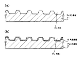
図7(a)は、この光ディスクにおける光記録ないしは光再生の状態を示す模式斜視図である。
光ディスクDCは、中心部にセンターホールCHが穿設された円板状をなし、図7(a)において、例えば矢印DRで示す方向に回転駆動される。
【0006】
図7(b)は光ディスクの模式断面図であり、図7(c)はこの光ディスクDCの要部の拡大断面図である。
この光ディスクは、厚さが約1.1mmの例えばポリカーボネートからなるディスク基板101の一主面に、凹部101rが形成され、凹部101rを含む凹凸面に沿って光記録層102が形成されて成る。
例えば相変化型の光ディスクDCにおいては、その光記録層102は、例えば誘電体膜、相変化膜、誘電体膜および反射膜などの積層体によって構成される。また、光記録層102の上層に、例えば0.1mmの膜厚の光透過層103が形成される。
【0007】
この光ディスクDCに対する情報の記録あるいは再生にあっては、光ディスクDCの光透過層103側から、光記録層102に、開口数が0.78以上例えば0.85の対物レンズOLによって、波長450nm以下例えば380〜420nmのレーザー光による光LTが集光照射される。
記録情報の再生時においては、光記録層102で反射された戻り光が受光素子で受光され、信号処理回路により所定の信号を生成して、再生信号を得る。
【0008】
この光ディスクの光記録層102は、ディスク基板101の表面に形成された上述の凹部101rに起因した凹凸形状を有している。
凹部101rは、例えば所定のピッチで例えば螺旋状をなす連続溝あるいは円形状の溝となっており、この凹凸形状によりトラック領域が区分される。
このトラック領域を区分する凹凸形状の凹部と凸部は、一方はランド、他方グルーブと呼ばれる。ランドとグルーブの両者に情報を記録するランド・グルーブ記録方式を適用することで大容量化が可能である。また、ランドとグルーブのいずれか一方のみを記録領域とすることも可能である。
【0009】
また、例えば、ディスク基板101に形成された凹部101rに起因する凹凸形状を記録データに対応する長さを有するピットとして、再生専用(ROM)型の光ディスクとすることもできる。
【0010】
ところで、光記録層を構成する記録材料として、非化学量論組成の金属酸化物の酸化錫(SnOz ,z<2)が使用できることが報告されている(非特許文献1参照)。
これは、レーザー光などの光を照射したときに生じる酸化反応により、光学定数が変化することを利用したものであると考えられている。
【0011】
【非特許文献1】
Journal of Materials Science Letters 19,2000,1833−1835
【0012】
【発明が解決しようとする課題】
しかしながら、記録材料として錫(Sn)を用いる場合、開口数が0.8程度の対物レンズを用い、波長380nm〜420nm程度の短波長光レーザー光を用いて情報の記録を行うとき、良好な形状の記録マークが形成されず、ジッター大きくなるという問題がある。
【0013】
本発明の第1の目的は、Snを記録材料として用いる場合において、上述したジッタ−の改善であり、第2の目的は、高温高湿度下においても、記録特性の安定化を図ることができ、保存安定性の向上を図ることができて良好な記録が可能な光記録媒体を提供することである。
【0014】
【課題を解決するための手段】
本発明による光記録媒体は、トラック領域を区分する凹凸形状が表面に形成された基板の、その凹凸形状の形成面に、少なくとも光記録層と、該光記録層上に形成された光透過層とを有し、その光記録層が、少なくとも錫(Sn)、窒素(N)および酸素(O)の化合物組成Snx Ny Oz (x,y,zは原子%)より成り、x,y,zが、
30<x<70(原子%)、1<y<20(原子%)、20<z<60(原子%)に選定された構成とする。
この構成としたことにより、ジッターの改善が図られた。
【0015】
また、本発明による光記録媒体は、上述した光記録媒体におけると同様のトラック領域を区分する凹凸形状が表面に形成された基板の、その凹凸形状の形成面に形成される光記録層にあって、その光記録層が、錫(Sn)、窒素(N)および酸素(O)の化合物にパラジウム(Pd)を含有する(Snx Ny Oz )1-a Pda 組成物(x,y,z,aは原子%)より成り、x,y,z,aが、
30<x<70(原子%)、1<y<20(原子%)、20<z<60(原子%)、1<a<20(原子%)に選定された構成とする。
この構成によって、ジッターの改善のみならず、特に、高温高湿度下での記録特性の変化も抑制された。これは、Pdの添加により記録時に溶融した記録膜の粘性が高められたことによると考えられる。
【0016】
【発明の実施の形態】
以下、本発明の実施の形態に係る光記録媒体(光ディスク)の実施の形態について詳細に説明する。しかしながら、本発明は、この実施形態例に限定されるものではない。
【0017】
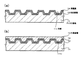
〔第1の実施の形態〕
図1(a)は、この実施の形態に係る光ディスクDCにおける光記録ないしは光再生の状態を示す模式斜視図である。
光ディスクDCは、センターホールCHが穿設された円板状をなし、図1(a)において、例えば矢印DRで示す方向に回転駆動される。
図1(b)はこの光ディスクDCの模式断面図であり、図1(c)は図1(b)の要部の拡大断面図である。
光ディスクDCは、センターホールCHを有する円板状をなし、厚さ約1.1mmの例えばポリカーボネートから成るディスク基板11の一主面に、凹部11rが設けられている。この凹部11rを含む凹凸に沿って光記録層12が形成され、この光記録層12上には、光透過層13が形成されている。
【0018】
光記録層12は、少なくとも錫(Sn)、窒素(N)、酸素(O)の化合物を有する。
この化合物の組成、Snx Ny Oz は、30<x<70(原子%)、1<y<20(原子%)、20<z<60(原子%)とされる。
光記録層12の膜厚は、10nm〜200nmの範囲であり、例えば30nm〜60nm程度である。
【0019】
光記録層12上の光透過層13は、例えば膜厚が0.1mmとされる。光透過層13は、例えば、紫外線硬化樹脂の塗布膜を硬化することによって形成される。あるいは、例えば粘着剤層が積層されたポリカーボネートなどの光透過性樹脂フイルムを、その粘着剤層によって光記録層12に貼り合わせることによって構成される。
【0020】
この実施形態における光ディスクDCに対する情報の記録または再生は、このディスクDCを、例えば図1(a)に矢印DRをもって示す方向に回転駆動させ、例えば、光ディスクDCの光記録層12に対して、例えば0.85±0.05の開口数の対物レンズOLを介して、例えば380nm〜420nmの波長のレーザー光LTを、光透過層13側から光記録層12に集光照射することによって行う。
【0021】
光ディスクの記録時においては、光記録層12に、例えば上述したレーザー光LTを照射し、その光照射部分に記録マークを形成する。この記録マークは、上述したレーザー光LTの照射によって酸化反応が生じ、これによって光記録層12の光照射部の光学定数が変化することによって形成されると思われる。
【0022】
また、光ディスクの再生時においては、光記録層12に照射され、記録マークにおける光学定数の変化によって変調された例えば戻り光が、受光素子で受光され、信号処理回路により所定の信号に生成され、再生信号として取り出される。
【0023】
この光ディスクにおいては、光記録層12は、ディスク基板11の表面に形成された凹部11rに起因した凹凸形状を有している。
例えば、ディスク基板11に形成された凹部11rは所定のピッチの螺旋状すなわちスパイラル状の連続溝、あるいは同心円形状の溝となっており、この凹凸形状によりトラック領域が区分される。
この例えば連続溝あるいは同心円形溝のピッチ(凹部の中央から隣接する凹部の中央までの距離)は、例えば0.32μm程度とされる。
【0024】
また、トラック領域を区分する凹凸形状の凹部と凸部とは、一方はランド、他方は、グルーブと呼ばれる。そして、ランドとグルーブの両者に情報を記録するランド・グルーブ記録方式を適用することで大容量化が可能である。しかしながら、ランドとグルーブのいずれか一方のみを記録領域とすることもできる。
この凹凸形状の深さは、数nm〜100nm程度であり、例えばグルーブ記録方式の場合には20nm、ランド・グルーブ記録方式の場合には40nmなどに設定することができる。
【0025】
因みに、記録材料として酸化錫(SnOz(z<2))を用いた場合、X線回折の実験から、膜中に、ある程度の大きさの粒径が存在していることがわかっている。この粒子は、光ディスクとして用いた場合のノイズ成分に寄与することから、前述したように、大容量化を図って、対物レンズを高開口数化し、レーザー光を短波長化したときに、粒子の影響が大きくなり、このために、ジッターが大きくなるものと考えられる。
【0026】
この実施形態の光ディスクは、記録材料として少なくとも錫、窒素および酸素の化合物、すなわち窒素(N)を添加したことによって、X線回折のピークが消失することがわかった。これは、光記録膜中の粒径が小さくなっていることを示すものである。
このように、粒径が小さくなったことにより、ノイズ成分となる粒子の影響が小さくなることから、この光ディスクにおいては、対物レンズを高開口数化し、レーザー光を短波長化してもジッターの抑制を図ることができることになる。
【0027】
そして、この光ディスクにおける光記録層として用いる錫(Sn)、窒素(N)および酸素(O)の化合物の組成は、窒素(N)の組成比yは、1<y<20(原子%)とする。
これは、1原子%以下では、粒径を小さくする効果が小さくなること、また20原子%以上であると、光記録層の光吸収率が低下して、光照射時に光定数を変化させるだけの温度上昇を来すに大きな光パワーを必要とすること、すなわち感度の低下を来すことによる。
【0028】
また、上述した化合物における酸素(O)の組成比zは、20<z<60(原子%)とする。
これは、20原子%以下では、光照射時に、酸化が不足となり、また、60原子%以上では、光記録層の光吸収率が低下してしまい、光照射時に光定数を変化させるだけの温度上昇を来すに大きな光パワーを必要とすること、すなわち感度の低下を来すことによる。
【0029】
このように、本発明による光記録層として、錫(Sn)、窒素(N)および酸素(O)の化合物の組成は、窒素(N)の化合物を用いる場合、組成Snx Ny Oz が、30<x<70(原子%)、1<y<20(原子%)、20<z<60(原子%)とする。
そして、この組成とすることにより、対物レンズの高開口数化、用いるレーザー光の短波長化によってもジッターを抑制する効果の増加が図られる。
【0030】
次に、この実施形態に係る光ディスクの製造方法について説明する。
まず、図2(a)に示すように、ディスク基板に凹凸形状を転写形成するためのスタンパ10を形成する。すなわち、このスタンパ10の表面には、図1で示したディスク基板11の凹部11rの反転パターンである凸部10pが形成されている。
【0031】
このスタンパ10は、次の方法によって得ることができる。
まず、ガラス基板の表面研磨された平滑面上に、例えばポジティブ型のフォトレジストをスピンコート等によって塗布する。このフォトレジスト層に対して、目的とする例えば螺旋形状あるいは同心円状など、ディスク基板の凹凸形状に対応する形状のパターンを露光し、その後、このフォトレジスト層を例えばアルカリ性の現像液で現像処理する。このようにして、パターン化されたフォトレジスト層によって、ディスク基板の凹凸形状のパターンに対応するパターンのレジスト膜が形成された原盤を得る。
【0032】
次に、この原盤上にニッケルなどの金属層を、無電解メッキおよびメッキによって所定厚さに堆積する。その後、この金属層を、原盤から剥離する。このようにすると、上述した原盤の凹凸の反転による凹凸を有するメッキ層から成るスタンパ10、あるいは、マスタースタンパ、マザ−スタンパ10を形成して、目的とするスタンパ10を転写して形成する。
【0033】
次に、このスタンパ10を、例えばディスク基板11を射出成形によって形成するための金型のキャビティ内に配置して例えばポリカーボネート(PC)による射出成形を行う。このようにして、図2(b)に示すように、スタンパ10の凹凸面上にディスク基板11を形成する。
このようにして、表面に、スタンパ10の凸部10pのパターンが転写されて、逆パターンの凹凸である凹部11rが形成されたディスク基板11が成形される。
【0034】
このようにして成形されたディスク基板11を、スタンパ10から離型し、その凹凸形成面に、空気や窒素ガスなどのガスを吹き付けてダストを除去した後、図3(a)に示すように、例えばスパッタリング法により、錫(Sn)、窒素(N)および酸素(O)の所定の組成比の化合物層を堆積させ、光記録層12を形成する。
【0035】
次に、図3(b)に示すように、光記録層12上に、光透過層13を、紫外線硬化樹脂などの光透過性樹脂材を塗布して硬化することによって形成するか、あるいは、ポリカーボネートなどの光透過性樹脂フイルムを、粘着剤層で貼り合わせることによって形成する。
このようにして、図1で示した構成の光ディスク11を製造することができる。
【0036】
この本発明による光ディスク11は、高開口数の対物レンズを用い、短波長レーザー光による情報記録を行う場合においても、ジッターが抑制され、良好な記録を行うことができた。
【0037】
次に、本発明による光記録媒体の、他の実施の形態例として第2の実施の形態を説明する。
この第2の実施の形態においては、光記録媒体に対して、情報記録、すなわち記録マークの形成を行う場合、レーザー光の照射によって記録層が昇温加熱されることによって光透過層13を構成する上述した粘着剤層が変質するおそれが有る場合に対処した構成によるものである。
【0038】
〔第2の実施の形態〕
図4は、この実施形態に係る光ディスクの模式断面図である。
この実施の形態に係る光ディスクは、実質的に上述した第1の実施形態に係る光ディスクと同様であるが、光記録層12と光透過層13との間に、光記録層12を保護する保護膜14を介在させた構成とした場合である。
【0039】
この実施の形態においても、例えば厚さが約1.1mmの例えばポリカーボネートからなるディスク基板11の一主面に、凹部11rが形成される。また、凹部11rを含む凹凸面に沿って光記録層12が形成されている。
この実施の形態においても、第1の実施の形態におけると同様に、その光記録層12は、少なくとも錫(Sn)、窒素(N)および酸素(O)の化合物を有する。好ましくは、錫(Sn)、窒素(N)および酸素(O)の組成が、 この化合物の組成、Snx Ny Oz は、30<x<70(原子%)、1<y<20(原子%)、20<z<60(原子%)とされる。
この光記録層12の膜厚は、10nm〜200nmの範囲であり、この場合例えば50nm〜60nm程度である。
【0040】
そして、この実施の形態においては、この光記録層12上に、例えば酸化シリコンなどの光透過性誘電体膜より成る保護膜14が形成される。
この保護膜14の膜厚は、5nm〜100nmの範囲、例えば30nmに選定される。
【0041】
この保護膜14上には、例えば0.1mmの膜厚の光透過層13が形成される。この光透過層13は、例えば粘着剤が積層されたポリカーボネートなどの光透過性樹脂フイルムを、その粘着剤層によって保護膜14上に貼り合わせることによって構成される。
【0042】
この実施の形態におけるように、保護膜14を配置する構成による場合、記録マークの形成における光照射によって、高熱状態とされた場合においても、保護膜14の存在によって、光透過層13における変質の、光記録層12への影響を遮断する効果を奏することができる。
【0043】
次に、この第2の実施の形態における光ディスクの製造方法について説明する。
まず、図5(a)に示すように、第1実施形態において説明した手順により、トラック領域を区分する凹部11rを含む凹凸形状が表面に形成されたにディスク基板11を形成する。
【0044】
次に、このディスク基板11の凹凸形状の形成面に、前述したと同様に、空気や窒素ガスなどのガスを吹き付けてダストを除去した後、図5(b)に示すように、例えばスパッタリング法などにより、錫、窒素および酸素の化合物による上述した組成の光記録層12を形成する。
【0045】
次に、図6(a)に示すように、例えばスパッタリング法などにより、酸化シリコンを堆積させ、保護膜14を形成する。
その後、図6(b)に示すように、保護膜14上に、ポリカーボネートなどの光透過性樹脂フイルムを粘着剤層で貼り合わせ、光透過層13を形成する。
このようにして、図4で示めした構成による光ディスクすなわち光記録媒体を製造することができる。
【0046】
この第2の実施における形態の光ディスクによれば、第1の実施形態におけると同様に、錫を記録材料として用いる場合に高開口数の対物レンズにより短波長のレーザー光などの光を照射して情報を記録してもジッターを抑制して良好に記録することができる。
【0047】
上述した本発明による光ディスク、すなわち光記録媒体をその具体的実施例を挙げて説明する。
(実施例1)
トラック領域を区分する凹凸形状が表面に形成されたディスク基板を形成した。凹凸形状は、0.32μm のピッチでスパイラル状に形成された連続溝とし、凹凸形状の深さは20nmとした。得られたディスク基板の凹凸形状の形成面上に、スパッタリングによりSnx Ny Oz (x=31原子%、y=10原子%、z=59原子%)を、この組成比となるように、50nmの膜厚で堆積させて光記録層を形成し、さらにその上層に酸化シリコンを30nmの膜厚で堆積させて保護膜を形成し、その上層にポリカーボネートなどの光透過性樹脂フイルムを粘着剤層で貼り合わせて0.1mmの厚さの光透過層を形成した。このようにして、光ディスクのサンプルAを作製した。
このサンプルAに対して、発振波長が405nmである記録再生用のレーザー光を、開口数が0.85である対物レンズにより光ディスクの光記録層に集光する光系を有する評価装置により、ビット長0.13μmのランダム信号を記録した。
このときの光ディスクに記録された信号のジッターは、9%であった。
【0048】
(比較例1)
実施例1と同様の構成とするものの、その光記録層の組成を、Snx Ny Oz (x=30原子%、y=10原子%、z=60原子%)と変更して、光ディスクのサンプルBを作製した。
このサンプルBに対して、実施例1に記載した評価装置により、ビット長0.13μmのランダム信号を記録した。このときのジッターは15%であった。
因みに、一般にジッターは、13%以下でなければ、正確な再生が困難であることから、ジッターは、13%以下にであることが、光記録媒体例えば光ディスクにおいて要求されるものである。
【0049】
(比較例2)
実施例1と同様の構成とするものの、その光記録層の組成を、Snx Ny Oz (x=25原子%、y=10原子%、z=65原子%)と変更して、光ディスクのサンプルCを作製した。
このサンプルCに対して、実施例1に記載した評価装置によりピット長0.13μmのランダム信号を記録したが、信号が記録されず、ジッターの測定は不能であった。
【0050】
(実施例2)
実施例1と同様の構成とするものの、その光記録層の組成を、Snx Ny Oz (x=69原子%、y=10原子%、z=21原子%)と変更して、光ディスクのサンプルDを作製した。
このサンプルDに対して、実施例1に記載した評価装置により、ビット長0.13μmのランダム信号を記録した。このときのジッターは10%であった。
【0051】
(比較例3)
実施例1と同様の構成とするものの、その光記録層の組成を、Snx Ny Oz (x=70原子%、y=10原子%、z=20原子%)と変更して、光ディスクのサンプルEを作製した。
このサンプルEに対して、実施例1に記載した評価装置により、ビット長0.13μmのランダム信号を記録した。このときのジッターは16%であり、13%を超えることから、前述したように、不適当であることが分かった。
【0052】
(比較例4)
実施例1と同様の構成とするものの、その光記録層の組成を、Snx Ny Oz (x=75原子%、y=10原子%、z=15原子%)と変更して、光ディスクのサンプルFを作製した。
このサンプルFに対して、実施例1に記載した評価装置によりピット長0.13μmのランダム信号を記録したが、信号が記録されず、ジッターの測定は不能であった。
【0053】
(実施例3)
実施例1と同様の構成とするものの、その光記録層の組成を、Snx Ny Oz (x=45原子%、y=2原子%、z=53原子%)と変更して、光ディスクのサンプルGを作製した。
このサンプルGに対して、実施例1に記載した評価装置により、ビット長0.13μmのランダム信号を記録した。このときのジッターは10%であった。
【0054】
(比較例5)
実施例1と同様の構成とするものの、その光記録層の組成を、Snx Ny Oz (x=45原子%、y=1原子%、z=54原子%)と変更して、光ディスクのサンプルHを作製した。
このサンプルHに対して、実施例1に記載した評価装置により、ビット長0.13μmのランダム信号を記録した。このときのジッターは14%であり、13%を超えることから、不適当であることが分かった。
【0055】
(実施例4)
実施例1と同様の構成とするものの、その光記録層の組成を、Snx Ny Oz (x=45原子%、y=19原子%、z=36原子%)と変更して、光ディスクのサンプルIを作製した。
このサンプルIに対して、実施例1に記載した評価装置により、ビット長0.13μmのランダム信号を記録した。このときのジッターは10%であった。
【0056】
(比較例6)
実施例1と同様の構成とするものの、その光記録層の組成を、Snx Ny Oz (x=45原子%、y=20原子%、z=35原子%)と変更して、光ディスクのサンプルJを作製した。
このサンプルJに対して、実施例1に記載した評価装置により、ビット長0.13μmのランダム信号を記録した。このときのジッターは14%であり、不十分な結果となった。
【0057】
上述した本発明による実施例と、比較例の各サンプルのジッターの測定によって明らかなように、本発明による光記録層を、錫(Sn)、窒素(N)および酸素(O)の化合物を有し、その組成Snx Ny Oz が、30<x<70(原子%)、1<y<20(原子%)、20<z<60(原子%)とした光記録媒体は、ジッターの改善が図られることが分かる。
【0058】
すなわち、上述した第1および第2の実施形態においては、ジッターの改善を図ることができるものであるが、上述した実施の形態におけるように、酸化窒化錫Snx Ny Oz のみによるときは、レーザー光の照射によって溶融した状態では、その粘性が比較的低い。このため、ジッターの改善に制約が生じたり、高温高湿下での保存性の改善に制約が生じる。
これに対して、更に、本発明においては、高温、高湿に耐性が大で、その記録マークの鮮鋭度を高めて、ジッターの改善と、保存安定性を高める構成とすることができる。
この構成による本発明による光記録媒体は、その記録層として、Snx Ny Oz が、30<x<70(原子%)、1<y<20(原子%)、20<z<60(原子%)の化合物に、高融点金属のPdを1原子%〜20原子%混合させた構成とする。
すなわち、この構成においては、レーザー光照射による記録時において、記録層が溶融したときの粘性を高めて、流動の発生による記録マークの鮮鋭度の低下、位置の変動を改善し、ジッターの、より改善と、保存性を高めるものである。
【0059】
この構成による光記録媒体の実施の形態を説明する。
〔第3の実施の形態〕
この実施の形態においても、第1の実施の形態で説明したと同様に、図1(a)でその模式斜視図を示すように、光ディスクDCは、センターホールCHが穿設された円板状をなし、例えば厚さ約1.1mmの例えばポリカーボネートから成るディスク基板11の一主面に、凹部11rが設けられている。この凹部11rを含む凹凸に沿って図1(b)および(c)で示すように、光記録層12が形成され、この光記録層12上には、光透過層13が形成されている。
【0060】
光記録層12は、少なくとも錫(Sn)、窒素(N)、酸素(O)の化合物(Snx Ny Oz は、30<x<70(原子%)、1<y<20(原子%)、20<z<60(原子%))に、Pdを加えた混合物を有する。このPdの濃度は、1原子%以上、20原子%以下とする。
光記録層12の膜厚は、第1の実施の形態におけると同様に、10nm〜200nmの範囲であり、例えば30nm〜60nm程度である。
【0061】
また、光記録層12上に例えば膜厚が0.1mmの光透過層13が形成される。この光透過層13は、例えば、紫外線硬化樹脂の塗布膜を硬化することによって形成される。あるいは、例えば粘着剤層が積層されたポリカーボネートなどの光透過性樹脂フイルムを、その粘着剤層によって光記録層12に貼り合わせることによって構成される。
【0062】
この実施の形態における光ディスクDCに対する情報の記録または再生においても、このディスクDCを、例えば図1(a)に矢印DRをもって示す方向に回転駆動させ、例えば、光ディスクDCの光記録層12に対して、例えば0.85±0.05の開口数の対物レンズOLを介して、例えば380nm〜420nmの波長のレーザー光LTを、光透過層13側から光記録層12に集光照射することによって行う。
【0063】
光ディスクの記録時においては、光記録層12に、例えば上述したレーザー光LTを照射し、その光照射部分に記録マークを形成する。この記録マークは、前述したように、レーザー光LTの照射によって酸化反応が生じ、これによって光記録層12の光照射部の光学定数が変化することによって形成されると考えられる。
【0064】
また、光ディスクの再生時においては、光記録層12に照射され、記録マークにおける光学定数の変化によって変調された例えば戻り光が、受光素子で受光され、信号処理回路により所定の信号に生成され、再生信号として取り出される。
【0065】
この光ディスクにおいても、光記録層12は、ディスク基板11の表面に形成された凹部11rに起因した凹凸形状を有している。
例えば、ディスク基板11に形成された凹部11rは所定のピッチの螺旋状すなわちスパイラル状の連続溝、あるいは同心円形状の溝となっており、この凹凸形状によりトラック領域が区分される。
この例えば連続溝あるいは同心円形溝のピッチ(凹部の中央から隣接する凹部の中央までの距離)は、例えば0.32μm程度とされる。
【0066】
また、トラック領域を区分する凹凸形状の凹部と凸部とは、一方はランド、他方は、グルーブと呼ばれる。そして、ランドとグルーブの両者に情報を記録するランド・グルーブ記録方式を適用することで大容量化が可能である。しかしながら、ランドとグルーブのいずれか一方のみを記録領域とすることもできる。
この凹凸形状の深さは、数nm〜100nm程度であり、例えばグルーブ記録方式の場合には20nm、ランド・グルーブ記録方式の場合には40nmなどに設定することができる。
【0067】
この実施の形態による光ディスクは、記録材料として、少なくとも錫、窒素およびO2 の化合物に、Pdを混合したことにより、レーザー光照射することによって、記録層が溶融したときにおける粘性を高められ、記録マークの位置、形状の変動が抑制されることから、高密度記録化が図られる。すなわち、大容量化のために、対物レンズの高開口数化、照射レーザー光の短波長化によってもジッターの抑制を図ることができる。また、高温高湿下での記録特性の改善、保存安定性が図られる。
【0068】
この実施形態の光ディスクにおける光記録層を構成する錫(Sn)、窒素(N)、酸素(O)の化合物に加えるPdの濃度は、1原子%〜20原子%に選定する。これは、1原子%未満では、流動の抑制効果が小さくなってしまい、上述した保存安定性の改善が十分でなくなる。また、20原子%を超えると、融点および熱伝導率が大となり過ぎて、記録感度の低下を来すという不都合が生じる。
そこで、Pdの濃度は、1原子%〜20原子%に選定する。
【0069】
この実施の形態に係る光ディスクの製造方法について説明する。
この場合においても、図2で説明したと同様の方法によって、スタンパ10を形成する。すなわち、このスタンパ10の表面には、図1で示したディスク基板11の凹部11rの反転パターンの凸部10pが形成されている。
【0070】
次に、このスタンパ10を、例えばディスク基板11を射出成形によって形成するための金型のキャビティ内に、スタンパ10を配置して例えばポリカーボネート(PC)による射出成形を行う。このようにして、図2(b)に示すように、スタンパ10の凹凸面上にディスク基板11を形成する。
このようにして、表面に、スタンパ10の凸部10pのパターンが転写して、逆パターンの凹凸である凹部11rが形成されたディスク基板11が成形される。
【0071】
このようにして成形されたディスク基板11を、スタンパ10から離型し、その凹凸形成面に、空気や窒素ガスなどのガスを吹き付けてダストを除去した後、図3(a)に示すように、例えばスパッタリング法により、錫(Sn)、窒素(N)および酸素(O)の所定の組成比の化合物に、Pdを所定の添加量をもって混合した材料層を堆積させ、光記録層12を形成する。
【0072】
次に、図3(b)で示すように、前述した第1の実施の形態における製造方法で説明したと同様の手順および方法によって、光記録層12上に、光透過層13を形成する。
このようにして、図1で示した構成の光ディスク11を製造することができる。
【0073】
次に、第4の実施の形態を説明する。
この第4の実施の形態においては、上述した第3の実施の形態による光記録媒体において、情報記録、すなわち記録マークの形成を行う場合、レーザー光の照射によって記録層が昇温加熱されることによって光透過層13を構成する上述した粘着剤層が変質するおそれが有る場合に対処した構成によるものである。
【0074】
〔第4の実施の形態〕
この実施の形態における光ディスクは、図4で説明したと同様の模式的断面図を有する。
この実施の形態に係る光ディスクは、実質的に上述した第3の実施形態に係る光ディスクと同様であるが、光記録層12と光透過層13との間に、光記録層12を保護する保護膜14を介在させた構成とした場合である。
【0075】
この実施の形態においても、例えば厚さが約1.1mmの例えばポリカーボネートからなるディスク基板11の一主面に、凹部11rが形成される。また、凹部11rを含む凹凸面に沿って光記録層12が形成されている。
この実施の形態においても、第3の実施の形態におけると同様に、光記録層12が、Snx Ny Oz で、30<x<70(原子%)、1<y<20(原子%)、20<z<60(原子%)とされる化合物に、1〜20原子%のPdが混合された構成による。
この光記録層12の膜厚は、10nm〜200nmの範囲であり、この場合例えば30nm〜60nm程度である。
【0076】
そして、この実施の形態においても、この光記録層12上に、例えば酸化シリコンなどの光透過性誘電体膜より成る保護膜14が形成される。
この保護膜14の膜厚は、5nm〜100nmの範囲、例えば30nmに選定される。
【0077】
この保護膜14上には、例えば0.1mmの膜厚の光透過層13が形成される。この光透過層13は、例えば粘着剤が積層されたポリカーボネートなどの光透過性樹脂フイルムを、その粘着剤層によって保護膜14上に貼り合わせることによって構成される。
【0078】
この実施の形態におけるように、保護膜14を配置する構成による場合、記録マークの形成における光照射によって、高熱状態とされた場合においても、保護膜14の存在によって、光透過層13における変質によるノイズの増加に起因する記録再生特性の悪化を抑制することができる。
【0079】
次に、この実施の形態における光ディスクの製造方法について説明する。
まず、図5(a)に示すように、第1実施形態において説明した手順により、トラック領域を区分する凹部11rを含む凹凸形状が表面に形成されたディスク基板11を形成する。
【0080】
次に、このディスク基板11の凹凸形状の形成面に、前述したと同様に、空気や窒素ガスなどのガスを吹き付けてダストを除去した後、図5(b)に示すように、例えばスパッタリング法などにより、錫、窒素および酸素の化合物にPdの混合による上述した組成の光記録層12を形成する。
【0081】
次に、図6(a)に示すように、例えばスパッタリング法などにより、酸化シリコンを堆積させ、保護膜14を形成する。
その後、図6(b)に示すように、保護膜14上に、ポリカーボネートなどの光透過性樹脂フイルムを粘着剤層で貼り合わせ、光透過層13を形成する。
このようにして、図4で示した構成による光ディスクすなわち光記録媒体を製造することができる。
【0082】
上述したPdを混合した光記録層による本発明による光記録媒体を、その具体的実施例を挙げて説明する。
(実施例5)
トラック領域を区分する凹凸形状が表面に形成されたディスク基板を形成した。凹凸形状は、0.32μmのピッチでスパイラル状に形成された連続溝とし、凹凸形状の深さは20nmとした。得られたディスク基板の凹凸形状の形成面上に、スパッタリングにより(Snx Ny Oz )1-a Pda (x=31原子%、y=10原子%、z=59原子%、a=1原子%)を、この組成比となるように、50nmの膜厚で堆積させて光記録層を形成し、さらにその上層に酸化シリコンを30nmの膜厚で堆積させて保護膜を形成し、その上層にポリカーボネートなどの光透過性樹脂フイルムを粘着剤層で貼り合わせて0.1mmの厚さの光透過層を形成した。このようにして、光ディスクのサンプルKを作製した。
このサンプルKに対して、発振波長が405nmである記録再生用のレーザー光を、開口数が0.85である対物レンズにより光ディスクの光記録層に集光する光学系を有する評価装置により、ビット長0.13μmのランダム信号を記録した。
このときの光ディスクに記録された信号のジッターは、8%であった。
このサンプルKを、80℃、85%相対湿度で100時間保存したときの透過率変化は1%未満であった。
【0083】
(比較例7)
実施例5と同様の構成とするものの、その光記録層の組成を、(Snx Ny Oz )1-a Pda (x=31原子%、y=10原子%、z=59原子%、a=0.9原子%)と変更して、光ディスクのサンプルLを作製した。
このサンプルLに対して、実施例5に記載した評価装置により、ビット長0.13μmのランダム信号を記録した。このときのジッターは10%であった。
【0084】
(実施例6)
実施例5と同様の構成とするものの、その光記録層の組成を、(Snx Ny Oz )1-a Pda (x=31原子%、y=10原子%、z=59原子%、a=20原子%)と変更して、光ディスクのサンプルMを作製した。
このサンプルMに対して、実施例5に記載した評価装置により、ビット長0.13μmのランダム信号を記録した。このときのジッターは9%であった。
このサンプルMを、80℃、85%相対湿度で100時間保存したときの透過率変化は1%未満であった。
【0085】
(比較例8)
実施例5と同様の構成とするものの、その光記録層の組成を、(Snx Ny Oz )1-a Pda (x=31原子%、y=10原子%、z=59原子%、a=21原子%)と変更して、光ディスクのサンプルNを作製した。
このサンプルNに対して、実施例5に記載した評価装置により、ビット長0.13μmのランダム信号を記録した。このときのジッターは16%であった。
【0086】
上述した本発明によるサンプルK,Mと、比較例のサンプルL、Nのジッターの測定によって明らかなように、本発明による光記録層を、錫(Sn)、窒素(N)および酸素(O)の化合物に、Pdを混合した光記録媒体は、ジッターの改善と、高温高湿の耐性が高められることが分かる。
【0087】
尚、本発明による光記録媒体は、上述した実施の形態、実施例に限定されることなく、本発明構成において、例えば光カード、シート等の形状、これに伴う層の積層構造等、種々の変形変更がなされ得ることはいうまでもない。
【0088】
【発明の効果】
上述したように本発明による光記録媒体は、光記録層を構成する化合物組成を、Snx Ny Oz で、かつ30<x<70(原子%)、1<y<20(原子%)、20<z<60(原子%)とすることによって、冒頭に述べた錫を記録材料として用いる場合における高開口数の対物レンズにより短波長のレーザー光などの光を照射して情報を記録におけるジッターの問題の解決を図ることができたものである。
【0089】
更に、本発明による光記録媒体は、その光記録層を構成する化合物Snx Ny Oz に、Pdを混合したことにより、レーザー光照射することによって、記録層が溶融したときにおける粘性を高める効果を得ることができ、更に、記録マークの位置、形状の変動が抑制されることから、高密度記録化が図られる。すなわち、大容量化のために、対物レンズの高開口数化、照射レーザー光の短波長化によってもジッターの抑制を図ることができる。また、高温高湿化での記録特性の改善を図ることができ、より優れた記録特性を有する光記録媒体を構成することができる。
このように、本発明構成によれば、優れた記録特性大容量光記録媒体を得ることができるという大きな効果を奏するものである。
【図面の簡単な説明】
【図1】(a)は、本発明の実施の形態に係る光ディスクへの光の照射の様子を示す模式斜視図、(b)は、(a)のA−A’線上の模式的断面図、(c)は要部を拡大した断面図である。
【図2】(a)および(b)は、実施の形態に係る光ディスクの製造方法の製造工程を示す断面図である。
【図3】(a)および(b)は、本発明の実施の形態の工程図である。
【図4】本発明の実施の形態に係る光ディスクの模式断面図である。
【図5】(a)および(b)は、本発明の実施の形態に係る光ディスクの製造方法の製造工程図である。
【図6】(a)および(b)は、製造工程図である。
【図7】(a)は、従来例に係る光ディスクへの光の照射の様子を示す模式斜視図、(b)は、(a)のA−A’線上の模式的断面図、(c)は、要部の拡大断面図である。
【符号の説明】
10…スタンパ、10p…凸部、11…ディスク基板、11r…凹部、12…光記録層、13…光透過層、14…保護膜、CH…センターホール、DC…光ディスク、LT…レーザー光、OL…対物レンズ[0001]
BACKGROUND OF THE INVENTION
The present invention relates to an optical recording medium, and more particularly to an optical recording medium capable of high density recording.
[0002]
[Prior art]
In recent years, in the field of information recording, research and development relating to optical information recording methods have been active.
This optical information recording system has many advantages such as non-contact type recording / reproduction, read-only type, write-once type, rewritable type, etc. A wide range of applications from industrial use to consumer use is considered as a method that can be realized.
[0003]
Increasing the capacity of these optical recording media for various optical information recording systems, such as optical discs, is mainly due to the shortening of the wavelength of the laser light used as the light source used in the optical information recording system and the high numerical aperture (NA) lens. Has been achieved by reducing the spot size at the focal plane.
[0004]
For example, a CD (compact disc) has a laser beam wavelength of 780 nm, a lens numerical aperture (NA) of 0.45, and a capacity of 650 MB. Dedicated memory), the laser light wavelength is 650 nm; A. Is 0.6, and the capacity is 4.7 GB.
Furthermore, in the next generation optical disk system, an optical disk having a thin light transmission layer of about 0.1 mm, for example, is formed on the optical recording layer, and laser light is irradiated from the light transmission layer side. The wavelength is 450 nm or less; A. The capacity can be increased to 22 GB or more by setting the value to 0.78 or more.
[0005]
FIG. 7A is a schematic perspective view showing a state of optical recording or optical reproduction on this optical disc.
The optical disk DC has a disk shape with a center hole CH formed in the center, and is driven to rotate in the direction indicated by the arrow DR in FIG. 7A, for example.
[0006]
FIG. 7B is a schematic cross-sectional view of the optical disc, and FIG. 7C is an enlarged cross-sectional view of the main part of the optical disc DC.
This optical disk is formed by forming a
For example, in the phase change type optical disc DC, the
[0007]
In recording or reproducing information with respect to the optical disc DC, a wavelength of 450 nm or less is applied to the
At the time of reproducing recorded information, the return light reflected by the
[0008]
The
The
One of the concavo-convex concave and convex portions that divide the track region is called a land and the other groove. The capacity can be increased by applying a land / groove recording method for recording information on both the land and the groove. Further, only one of the land and the groove can be used as the recording area.
[0009]
Further, for example, a concavo-convex shape caused by the
[0010]
By the way, as a recording material constituting the optical recording layer, a non-stoichiometric metal oxide tin oxide (SnO) is used. z , Z <2) can be used (see Non-Patent Document 1).
This is considered to utilize the fact that the optical constant changes due to the oxidation reaction that occurs when light such as laser light is irradiated.
[0011]
[Non-Patent Document 1]
Journal of Materials Science Letters 19, 2000, 1833-1835
[0012]
[Problems to be solved by the invention]
However, when tin (Sn) is used as a recording material, an objective lens having a numerical aperture of about 0.8 is used, and when recording information using a short wavelength laser beam having a wavelength of about 380 nm to 420 nm, a good shape is obtained. However, there is a problem that jitter is increased.
[0013]
The first object of the present invention is to improve the above-mentioned jitter when Sn is used as a recording material, and the second object is to stabilize the recording characteristics even under high temperature and high humidity. An object of the present invention is to provide an optical recording medium capable of improving storage stability and capable of good recording.
[0014]
[Means for Solving the Problems]
The optical recording medium according to the present invention includes at least an optical recording layer and a light transmission layer formed on the optical recording layer on a surface on which the concave / convex shape for dividing the track region is formed. The optical recording layer has a compound composition Sn of at least tin (Sn), nitrogen (N) and oxygen (O). x N y O z (X, y, z is atomic%), and x, y, z
It is assumed that 30 <x <70 (atomic%), 1 <y <20 (atomic%), and 20 <z <60 (atomic%).
With this configuration, jitter was improved.
[0015]
In addition, the optical recording medium according to the present invention is suitable for an optical recording layer formed on the surface having the concavo-convex shape formed on the surface of the substrate having the concavo-convex shape separating the track regions as in the above-described optical recording medium. The optical recording layer contains palladium (Pd) in a compound of tin (Sn), nitrogen (N) and oxygen (O) (Sn x N y O z ) 1-a Pd a A composition (x, y, z, a is atomic%), where x, y, z, a are
It is assumed that 30 <x <70 (atomic%), 1 <y <20 (atomic%), 20 <z <60 (atomic%), and 1 <a <20 (atomic%).
With this configuration, not only the improvement of jitter but also the change in recording characteristics under high temperature and high humidity is suppressed. This is presumably because the viscosity of the recording film melted at the time of recording was increased by the addition of Pd.
[0016]
DETAILED DESCRIPTION OF THE INVENTION
Hereinafter, an embodiment of an optical recording medium (optical disk) according to an embodiment of the present invention will be described in detail. However, the present invention is not limited to this embodiment.
[0017]
[First Embodiment]
FIG. 1A is a schematic perspective view showing a state of optical recording or optical reproduction in the optical disc DC according to this embodiment.
The optical disk DC has a disk shape with a center hole CH formed therein, and is rotated in the direction indicated by the arrow DR in FIG.
FIG. 1B is a schematic cross-sectional view of the optical disc DC, and FIG. 1C is an enlarged cross-sectional view of the main part of FIG.
The optical disc DC has a disc shape having a center hole CH, and a
[0018]
The
Composition of this compound, Sn x N y O z Are 30 <x <70 (atomic%), 1 <y <20 (atomic%), and 20 <z <60 (atomic%).
The film thickness of the
[0019]
The
[0020]
For recording or reproducing information with respect to the optical disc DC in this embodiment, the disc DC is rotated in a direction indicated by an arrow DR in FIG. 1A, for example, and the
[0021]
At the time of recording on the optical disk, the above-described laser beam is applied to the
[0022]
Further, at the time of reproducing the optical disk, for example, return light that is irradiated to the
[0023]
In this optical disc, the
For example, the
The pitch of this continuous groove or concentric circular groove (distance from the center of the recess to the center of the adjacent recess) is, for example, about 0.32 μm.
[0024]
One of the concave and convex portions and the convex portion that divides the track area is called a land, and the other is called a groove. The capacity can be increased by applying a land / groove recording method for recording information on both the land and the groove. However, only one of the land and the groove can be used as the recording area.
The depth of the concavo-convex shape is about several nm to 100 nm, and can be set to, for example, 20 nm in the case of the groove recording method and 40 nm in the case of the land / groove recording method.
[0025]
Incidentally, when tin oxide (SnOz (z <2)) is used as a recording material, it is known from an X-ray diffraction experiment that a particle size of a certain size exists in the film. Since these particles contribute to noise components when used as an optical disk, as described above, when the capacity is increased, the objective lens is increased in numerical aperture, and the laser beam is shortened, The influence becomes large, and it is considered that the jitter becomes large due to this.
[0026]
In the optical disk of this embodiment, it was found that the peak of X-ray diffraction disappears by adding at least a compound of tin, nitrogen and oxygen, that is, nitrogen (N), as a recording material. This indicates that the particle size in the optical recording film is reduced.
In this way, since the influence of particles that become noise components is reduced by reducing the particle size, jitter is suppressed even if the objective lens has a high numerical aperture and the laser light has a shorter wavelength. Can be achieved.
[0027]
The composition of the compound of tin (Sn), nitrogen (N) and oxygen (O) used as the optical recording layer in this optical disc is such that the composition ratio y of nitrogen (N) is 1 <y <20 (atomic%). To do.
This is because when 1 atom% or less, the effect of reducing the particle size is reduced, and when it is 20 atom% or more, the optical absorptance of the optical recording layer is lowered and only the optical constant is changed during light irradiation. This is because a large optical power is required to increase the temperature, that is, the sensitivity is decreased.
[0028]
The composition ratio z of oxygen (O) in the above-described compound is 20 <z <60 (atomic%).
If it is 20 atomic% or less, oxidation is insufficient during light irradiation, and if it is 60 atomic% or more, the light absorption rate of the optical recording layer decreases, and the temperature is sufficient to change the optical constant during light irradiation. This is because it requires a large amount of optical power to increase, that is, the sensitivity decreases.
[0029]
Thus, the composition of the compound of tin (Sn), nitrogen (N) and oxygen (O) as the optical recording layer according to the present invention is the composition Sn when the compound of nitrogen (N) is used. x N y O z However, 30 <x <70 (atomic%), 1 <y <20 (atomic%), and 20 <z <60 (atomic%).
With this composition, the effect of suppressing jitter can be increased by increasing the numerical aperture of the objective lens and shortening the wavelength of the laser beam used.
[0030]
Next, an optical disk manufacturing method according to this embodiment will be described.
First, as shown in FIG. 2A, a
[0031]
This
First, for example, a positive photoresist is applied on a smooth surface of the glass substrate whose surface has been polished by spin coating or the like. The photoresist layer is exposed to a pattern having a shape corresponding to the concave / convex shape of the disk substrate, such as a target spiral shape or concentric circle shape, and then the photoresist layer is developed with an alkaline developer, for example. . In this way, a master having a patterned resist layer formed with a resist film having a pattern corresponding to the concavo-convex pattern of the disk substrate is obtained.
[0032]
Next, a metal layer such as nickel is deposited on the master to a predetermined thickness by electroless plating and plating. Then, this metal layer is peeled from the master. In this way, the
[0033]
Next, the
In this way, the pattern of the
[0034]
The
[0035]
Next, as shown in FIG. 3B, the
In this way, the
[0036]
The
[0037]
Next, a second embodiment will be described as another embodiment of the optical recording medium according to the present invention.
In the second embodiment, when information recording is performed on an optical recording medium, that is, a recording mark is formed, the
[0038]
[Second Embodiment]
FIG. 4 is a schematic cross-sectional view of the optical disc according to this embodiment.
The optical disc according to this embodiment is substantially the same as the optical disc according to the first embodiment described above, but protection for protecting the
[0039]
Also in this embodiment, the
Also in this embodiment, as in the first embodiment, the
The thickness of the
[0040]
In this embodiment, a
The thickness of the
[0041]
On the
[0042]
In the case where the
[0043]
Next, an optical disk manufacturing method according to the second embodiment will be described.
First, as shown in FIG. 5A, according to the procedure described in the first embodiment, the
[0044]
Next, after the dust is removed by blowing a gas such as air or nitrogen gas onto the uneven surface of the
[0045]
Next, as shown in FIG. 6A, silicon oxide is deposited by, eg, sputtering, and the
Thereafter, as shown in FIG. 6B, a light-transmitting resin film such as polycarbonate is bonded to the
In this manner, an optical disk, that is, an optical recording medium having the configuration shown in FIG. 4 can be manufactured.
[0046]
According to the optical disk of the second embodiment, as in the first embodiment, when tin is used as a recording material, light such as a short wavelength laser beam is irradiated by an objective lens having a high numerical aperture. Even if information is recorded, jitter can be suppressed and recording can be performed satisfactorily.
[0047]
The optical disk according to the present invention described above, that is, the optical recording medium will be described with specific examples.
Example 1
A disk substrate having a concavo-convex shape for dividing the track area formed on the surface was formed. The uneven shape was a continuous groove formed in a spiral shape at a pitch of 0.32 μm, and the depth of the uneven shape was 20 nm. Sn was formed by sputtering on the uneven surface of the obtained disk substrate. x N y O z (X = 31 atomic%, y = 10 atomic%, z = 59 atomic%) are deposited with a film thickness of 50 nm so as to have this composition ratio, and an optical recording layer is formed, and a silicon oxide layer is further formed thereon. Was deposited with a film thickness of 30 nm, and a light-transmitting resin film such as polycarbonate was bonded to the upper layer with an adhesive layer to form a light-transmitting layer having a thickness of 0.1 mm. In this way, Sample A of the optical disc was produced.
For this sample A, an evaluation apparatus having an optical system for condensing recording / reproducing laser light having an oscillation wavelength of 405 nm onto an optical recording layer of an optical disk by an objective lens having a numerical aperture of 0.85 A random signal with a length of 0.13 μm was recorded.
At this time, the jitter of the signal recorded on the optical disk was 9%.
[0048]
(Comparative Example 1)
Although the configuration is similar to that of Example 1, the composition of the optical recording layer is Sn. x N y O z Sample B of an optical disk was manufactured by changing (x = 30 atomic%, y = 10 atomic%, z = 60 atomic%).
With respect to this sample B, a random signal having a bit length of 0.13 μm was recorded by the evaluation apparatus described in Example 1. The jitter at this time was 15%.
Incidentally, since it is generally difficult to accurately reproduce the jitter unless the jitter is 13% or less, the jitter is required to be 13% or less in an optical recording medium such as an optical disc.
[0049]
(Comparative Example 2)
Although the configuration is similar to that of Example 1, the composition of the optical recording layer is Sn. x N y O z A sample C of an optical disc was manufactured by changing (x = 25 atomic%, y = 10 atomic%, z = 65 atomic%).
For this sample C, a random signal having a pit length of 0.13 μm was recorded by the evaluation apparatus described in Example 1. However, no signal was recorded, and jitter measurement was impossible.
[0050]
(Example 2)
Although the configuration is similar to that of Example 1, the composition of the optical recording layer is Sn. x N y O z The sample D of the optical disk was manufactured by changing (x = 69 atomic%, y = 10 atomic%, z = 21 atomic%).
For this sample D, a random signal having a bit length of 0.13 μm was recorded by the evaluation apparatus described in Example 1. The jitter at this time was 10%.
[0051]
(Comparative Example 3)
Although the configuration is similar to that of Example 1, the composition of the optical recording layer is Sn. x N y O z The sample E of the optical disc was manufactured by changing (x = 70 atomic%, y = 10 atomic%, z = 20 atomic%).
With respect to this sample E, a random signal having a bit length of 0.13 μm was recorded by the evaluation apparatus described in Example 1. The jitter at this time is 16% and exceeds 13%, which proves inappropriate as described above.
[0052]
(Comparative Example 4)
Although the configuration is similar to that of Example 1, the composition of the optical recording layer is Sn. x N y O z A sample F of an optical disc was manufactured by changing (x = 75 atomic%, y = 10 atomic%, z = 15 atomic%).
For this sample F, a random signal having a pit length of 0.13 μm was recorded by the evaluation apparatus described in Example 1. However, no signal was recorded, and jitter measurement was impossible.
[0053]
Example 3
Although the configuration is similar to that of Example 1, the composition of the optical recording layer is Sn. x N y O z The sample G of the optical disk was manufactured by changing (x = 45 atomic%, y = 2 atomic%, z = 53 atomic%).
A random signal having a bit length of 0.13 μm was recorded on the sample G by the evaluation apparatus described in Example 1. The jitter at this time was 10%.
[0054]
(Comparative Example 5)
Although the configuration is similar to that of Example 1, the composition of the optical recording layer is Sn. x N y O z The sample H of the optical disc was manufactured by changing (x = 45 atomic%, y = 1 atomic%, z = 54 atomic%).
For this sample H, a random signal having a bit length of 0.13 μm was recorded by the evaluation apparatus described in Example 1. The jitter at this time is 14% and exceeds 13%, which proves inappropriate.
[0055]
Example 4
Although the configuration is similar to that of Example 1, the composition of the optical recording layer is Sn. x N y O z Samples I of the optical disk were manufactured by changing the values to (x = 45 atomic%, y = 19 atomic%, z = 36 atomic%).
For this sample I, a random signal having a bit length of 0.13 μm was recorded by the evaluation apparatus described in Example 1. The jitter at this time was 10%.
[0056]
(Comparative Example 6)
Although the configuration is similar to that of Example 1, the composition of the optical recording layer is Sn. x N y O z A sample J of an optical disk was manufactured by changing (x = 45 atomic%, y = 20 atomic%, z = 35 atomic%).
For this sample J, a random signal having a bit length of 0.13 μm was recorded by the evaluation apparatus described in Example 1. The jitter at this time was 14%, which was an insufficient result.
[0057]
As is apparent from the measurement of the jitter of each of the examples according to the present invention and the comparative examples, the optical recording layer according to the present invention has a compound of tin (Sn), nitrogen (N), and oxygen (O). And its composition Sn x N y O z However, it can be seen that the optical recording medium in which 30 <x <70 (atomic%), 1 <y <20 (atomic%), and 20 <z <60 (atomic%) can improve jitter.
[0058]
That is, in the first and second embodiments described above, the jitter can be improved, but as in the above-described embodiment, tin oxynitride Sn. x N y O z In the case of only the above, the viscosity is relatively low in the melted state by laser light irradiation. For this reason, there are restrictions on the improvement of jitter, and there are restrictions on the improvement of storage stability under high temperature and high humidity.
On the other hand, in the present invention, it is possible to adopt a configuration that is highly resistant to high temperature and high humidity, improves the sharpness of the recording mark, and improves jitter and storage stability.
The optical recording medium according to the present invention having this configuration has Sn as its recording layer. x N y O z However, a compound of 30 <x <70 (atomic%), 1 <y <20 (atomic%), 20 <z <60 (atomic%) is mixed with 1 to 20 atomic% of refractory metal Pd. The configuration is as follows.
That is, in this configuration, at the time of recording by laser light irradiation, the viscosity when the recording layer is melted is increased, the sharpness of the recording mark is reduced due to the flow, the position fluctuation is improved, and the jitter is further improved. It improves and improves storage stability.
[0059]
An embodiment of an optical recording medium having this configuration will be described.
[Third Embodiment]
In this embodiment as well, as described in the first embodiment, as shown in the schematic perspective view of FIG. 1A, the optical disc DC has a disk shape with a center hole CH formed therein. A
[0060]
The
The film thickness of the
[0061]
Further, a
[0062]
Also in the recording or reproduction of information with respect to the optical disc DC in this embodiment, the disc DC is driven to rotate in the direction indicated by the arrow DR in FIG. 1A, for example, with respect to the
[0063]
At the time of recording on the optical disk, the above-described laser beam is applied to the
[0064]
Further, at the time of reproducing the optical disk, for example, return light that is irradiated to the
[0065]
Also in this optical disc, the
For example, the
The pitch of this continuous groove or concentric circular groove (distance from the center of the recess to the center of the adjacent recess) is, for example, about 0.32 μm.
[0066]
One of the concave and convex portions and the convex portion that divides the track area is called a land, and the other is called a groove. The capacity can be increased by applying a land / groove recording method for recording information on both the land and the groove. However, only one of the land and the groove can be used as the recording area.
The depth of the concavo-convex shape is about several nm to 100 nm, and can be set to, for example, 20 nm in the case of the groove recording method and 40 nm in the case of the land / groove recording method.
[0067]
The optical disc according to this embodiment has at least tin, nitrogen and O as recording materials. 2 By mixing Pd with this compound, the viscosity when the recording layer is melted can be increased by irradiating the laser beam, and the change in the position and shape of the recording mark can be suppressed. Figured. That is, in order to increase the capacity, jitter can also be suppressed by increasing the numerical aperture of the objective lens and shortening the wavelength of the irradiation laser beam. In addition, recording characteristics under high temperature and high humidity can be improved and storage stability can be achieved.
[0068]
The concentration of Pd added to the compound of tin (Sn), nitrogen (N), and oxygen (O) constituting the optical recording layer in the optical disk of this embodiment is selected from 1 atomic% to 20 atomic%. If the content is less than 1 atomic%, the effect of suppressing flow becomes small, and the above-described improvement in storage stability becomes insufficient. On the other hand, if it exceeds 20 atomic%, the melting point and the thermal conductivity become excessively large, resulting in a disadvantage that the recording sensitivity is lowered.
Therefore, the concentration of Pd is selected from 1 atomic% to 20 atomic%.
[0069]
A method for manufacturing an optical disk according to this embodiment will be described.
Also in this case, the
[0070]
Next, the
In this manner, the pattern of the
[0071]
The
[0072]
Next, as shown in FIG. 3B, a
In this way, the
[0073]
Next, a fourth embodiment will be described.
In the fourth embodiment, when recording information, that is, forming a recording mark, in the optical recording medium according to the third embodiment described above, the recording layer is heated and heated by laser light irradiation. This is because the above-described pressure-sensitive adhesive layer that constitutes the
[0074]
[Fourth Embodiment]
The optical disc in this embodiment has a schematic cross-sectional view similar to that described with reference to FIG.
The optical disc according to this embodiment is substantially the same as the optical disc according to the third embodiment described above, but protection for protecting the
[0075]
Also in this embodiment, the
Also in this embodiment, as in the third embodiment, the
The thickness of the
[0076]
Also in this embodiment, the
The thickness of the
[0077]
On the
[0078]
As in this embodiment, in the case of the configuration in which the
[0079]
Next, this The fruit A method of manufacturing an optical disc in the embodiment will be described.
First, as shown in FIG. 5 (a), a concavo-convex shape including a
[0080]
Next, after the dust is removed by blowing a gas such as air or nitrogen gas onto the uneven surface of the
[0081]
Next, as shown in FIG. 6A, silicon oxide is deposited by, eg, sputtering, and the
Thereafter, as shown in FIG. 6B, a light-transmitting resin film such as polycarbonate is bonded to the
Thus, in FIG. Showing Optical disk, ie optical recording medium The Can be manufactured.
[0082]
The optical recording medium according to the present invention using the optical recording layer mixed with Pd described above will be described with reference to specific examples.
(Example 5)
A disk substrate having a concavo-convex shape for dividing the track area formed on the surface was formed. Uneven shape is 0.32μ m The depth of the concavo-convex shape was 20 nm. (Snx Ny Oz) 1-a Pda (x = 31 atomic%, y = 10 atomic%, z = 59 atomic%, a = 1 atomic%) is formed on the surface of the disk substrate having the irregular shape by sputtering. Is deposited with a film thickness of 50 nm so as to have this composition ratio, and an optical recording layer is formed, and a protective film is formed by depositing silicon oxide with a film thickness of 30 nm on the upper layer, and polycarbonate is formed on the upper layer. A light-transmitting resin film such as the above was bonded with an adhesive layer to form a light-transmitting layer having a thickness of 0.1 mm. In this way, an optical disk sample K was produced.
This sample K In contrast, a recording / reproducing laser beam having an oscillation wavelength of 405 nm is condensed on an optical recording layer of an optical disk by an objective lens having a numerical aperture of 0.85. Optical system A random signal having a bit length of 0.13 μm was recorded by an evaluation apparatus having
The jitter of the signal recorded on the optical disk at this time was 8%.
When this sample K was stored at 80 ° C. and 85% relative humidity for 100 hours, the change in transmittance was less than 1%.
[0083]
(Comparative Example 7)
Although the configuration is similar to that of Example 5, the composition of the optical recording layer is (Sn x N y O z ) 1-a Pd a (X = 31 atomic%, y = 10 atomic%, z = 59 atomic%, a = 0.9 atomic%).
A random signal having a bit length of 0.13 μm was recorded on the sample L by the evaluation apparatus described in Example 5. The jitter at this time was 10%.
[0084]
(Example 6)
Although the configuration is similar to that of Example 5, the composition of the optical recording layer is (Sn x N y O z ) 1-a Pd a A sample M of an optical disc was manufactured by changing (x = 31 atomic%, y = 10 atomic%, z = 59 atomic%, a = 20 atomic%).
For this sample M, a random signal having a bit length of 0.13 μm was recorded by the evaluation apparatus described in Example 5. The jitter at this time was 9%.
When this sample M was stored at 80 ° C. and 85% relative humidity for 100 hours, the transmittance change was less than 1%.
[0085]
(Comparative Example 8)
Although the configuration is similar to that of Example 5, the composition of the optical recording layer is (Sn x N y O z ) 1-a Pd a The sample N of the optical disk was manufactured by changing (x = 31 atomic%, y = 10 atomic%, z = 59 atomic%, a = 21 atomic%).
A random signal having a bit length of 0.13 μm was recorded on the sample N by the evaluation apparatus described in Example 5. The jitter at this time was 16%.
[0086]
As is apparent from the measurement of the jitter of the samples K and M according to the present invention and the samples L and N of the comparative examples, the optical recording layer according to the present invention is made of tin (Sn), nitrogen (N) and oxygen (O). It can be seen that an optical recording medium in which Pd is mixed with the above compound can improve jitter and have high temperature and high humidity resistance.
[0087]
The optical recording medium according to the present invention is not limited to the above-described embodiments and examples, and in the configuration of the present invention, there are various types such as the shape of an optical card, a sheet, etc. Needless to say, deformation changes can be made.
[0088]
【The invention's effect】
As described above, the optical recording medium according to the present invention has Sn as a compound composition constituting the optical recording layer. x N y O z And 30 <x <70 (atomic%), 1 <y <20 (atomic%), and 20 <z <60 (atomic%). It was possible to solve the problem of jitter in recording information by irradiating light such as laser light having a short wavelength with an objective lens having a numerical aperture.
[0089]
Furthermore, the optical recording medium according to the present invention comprises the compound Sn constituting the optical recording layer. x N y O z In addition, by mixing Pd, it is possible to obtain an effect of increasing the viscosity when the recording layer is melted by irradiating the laser beam, and further, fluctuations in the position and shape of the recording mark are suppressed. High density recording is achieved. That is, in order to increase the capacity, jitter can also be suppressed by increasing the numerical aperture of the objective lens and shortening the wavelength of the irradiation laser beam. Further, the recording characteristics can be improved at high temperature and high humidity, and an optical recording medium having more excellent recording characteristics can be configured.
As described above, according to the configuration of the present invention, it is possible to obtain an excellent recording characteristic and large capacity optical recording medium.
[Brief description of the drawings]
1A is a schematic perspective view showing a state of light irradiation to an optical disc according to an embodiment of the present invention, and FIG. 1B is a schematic cross-sectional view taken along the line AA ′ in FIG. (C) is sectional drawing to which the principal part was expanded.
FIGS. 2A and 2B are cross-sectional views illustrating manufacturing steps of an optical disk manufacturing method according to an embodiment. FIGS.
FIGS. 3A and 3B are process diagrams of an embodiment of the present invention. FIGS.
FIG. 4 is a schematic cross-sectional view of an optical disc according to an embodiment of the present invention.
FIGS. 5A and 5B are manufacturing process diagrams of an optical disk manufacturing method according to an embodiment of the present invention. FIGS.
FIGS. 6A and 6B are manufacturing process diagrams. FIGS.
7A is a schematic perspective view showing a state of light irradiation to an optical disc according to a conventional example, FIG. 7B is a schematic cross-sectional view taken along the line AA ′ in FIG. These are the expanded sectional views of the principal part.
[Explanation of symbols]
DESCRIPTION OF
Claims (4)
少なくとも光記録層と、該光記録層上に形成された光透過層とを有し、
上記光記録層が、少なくとも錫(Sn)、窒素(N)および酸素(O)の化合物組成Snx Ny Oz (x,y,zは原子%)より成り、x,y,zが、
30<x<70(原子%)、1<y<20(原子%)、20<z<60(原子%)に選定されたことを特徴とする光記録媒体。On the formation surface of the concavo-convex shape of the substrate on which the concavo-convex shape for dividing the track region is formed on the surface,
Having at least an optical recording layer and a light transmission layer formed on the optical recording layer,
The optical recording layer comprises a compound composition Sn x N y O z (x, y, z is atomic%) of at least tin (Sn), nitrogen (N), and oxygen (O), and x, y, z are
30 <x <70 (atomic%), 1 <y <20 (atomic%), 20 <z <60 (atomic%).
少なくとも光記録層と、該光記録層上に形成された光透過層とが形成され、
上記光記録層が、錫(Sn)、窒素(N)および酸素(O)の化合物にパラジウム(Pd)を含有する(Snx Ny Oz )1-a Pda 組成物(x,y,z,aは原子%)より成り、x,y,z,aが、
30<x<70(原子%)、1<y<20(原子%)、20<z<60(原子%)、1<a<20(原子%)に選定されたことを特徴とする光記録媒体。On the formation surface of the concavo-convex shape of the substrate on which the concavo-convex shape for dividing the track region is formed on the surface,
At least an optical recording layer and a light transmission layer formed on the optical recording layer are formed,
The optical recording layer, tin (Sn), containing palladium (Pd) to a compound of nitrogen (N) and oxygen (O) (Sn x N y O z) 1-a Pd a composition (x, y, z, a are atomic%), and x, y, z, a are
30 <x <70 (atomic%), 1 <y <20 (atomic%), 20 <z <60 (atomic%), 1 <a <20 (atomic%) Medium.
Priority Applications (6)
| Application Number | Priority Date | Filing Date | Title |
|---|---|---|---|
| JP2003017877A JP3852408B2 (en) | 2002-07-09 | 2003-01-27 | Optical recording medium |
| PCT/JP2003/008538 WO2004005041A1 (en) | 2002-07-09 | 2003-07-04 | Optical recording medium |
| KR1020047004201A KR20050025123A (en) | 2002-07-09 | 2003-07-04 | Optical recording medium |
| CA002459838A CA2459838A1 (en) | 2002-07-09 | 2003-07-04 | Optical recording medium |
| US10/488,725 US7390546B2 (en) | 2002-07-09 | 2003-07-04 | Optical recording medium |
| TW092118603A TWI227482B (en) | 2002-07-09 | 2003-07-08 | Optical recording medium |
Applications Claiming Priority (2)
| Application Number | Priority Date | Filing Date | Title |
|---|---|---|---|
| JP2002200376 | 2002-07-09 | ||
| JP2003017877A JP3852408B2 (en) | 2002-07-09 | 2003-01-27 | Optical recording medium |
Publications (3)
| Publication Number | Publication Date |
|---|---|
| JP2004090610A JP2004090610A (en) | 2004-03-25 |
| JP2004090610A5 JP2004090610A5 (en) | 2005-04-07 |
| JP3852408B2 true JP3852408B2 (en) | 2006-11-29 |
Family
ID=30117416
Family Applications (1)
| Application Number | Title | Priority Date | Filing Date |
|---|---|---|---|
| JP2003017877A Expired - Fee Related JP3852408B2 (en) | 2002-07-09 | 2003-01-27 | Optical recording medium |
Country Status (6)
| Country | Link |
|---|---|
| US (1) | US7390546B2 (en) |
| JP (1) | JP3852408B2 (en) |
| KR (1) | KR20050025123A (en) |
| CA (1) | CA2459838A1 (en) |
| TW (1) | TWI227482B (en) |
| WO (1) | WO2004005041A1 (en) |
Families Citing this family (13)
| Publication number | Priority date | Publication date | Assignee | Title |
|---|---|---|---|---|
| JP3852420B2 (en) * | 2003-03-13 | 2006-11-29 | ソニー株式会社 | Optical recording medium |
| EP1657071B1 (en) | 2003-08-21 | 2013-02-27 | Mitsubishi Kagaku Media Co., Ltd. | Recording medium |
| JP4349248B2 (en) * | 2004-10-04 | 2009-10-21 | 株式会社日立製作所 | Optical information recording medium, reproducing method thereof and manufacturing method thereof |
| JP4696134B2 (en) * | 2005-05-30 | 2011-06-08 | パイオニア株式会社 | Resist material and electron beam recording resist material |
| JP4696113B2 (en) * | 2005-05-30 | 2011-06-08 | パイオニア株式会社 | Resist material and electron beam recording resist material |
| TWI322417B (en) | 2005-11-03 | 2010-03-21 | Princo Corp | Optical disc capable of suppressing vibration while reading/writing and the method of fabricating the same |
| WO2010068859A2 (en) * | 2008-12-12 | 2010-06-17 | Gibby Media Group | Sticker media disk |
| JP4859145B2 (en) * | 2008-12-25 | 2012-01-25 | 独立行政法人産業技術総合研究所 | Etching resist |
| US8302005B2 (en) * | 2009-01-14 | 2012-10-30 | Gibby Media Group | Optimizing playback of media content |
| JP2010218636A (en) * | 2009-03-17 | 2010-09-30 | Sony Corp | Method of manufacturing optical recording medium, and optical recording medium |
| JP5592621B2 (en) * | 2009-08-20 | 2014-09-17 | ソニー株式会社 | Optical recording medium |
| KR20120057629A (en) * | 2009-09-18 | 2012-06-05 | 소니 주식회사 | Recording layer for optical information recording medium, optical information recording medium, and sputtering target |
| US11275308B2 (en) * | 2016-03-04 | 2022-03-15 | Nanotronix Inc. | Photoexcitation method |
Family Cites Families (17)
| Publication number | Priority date | Publication date | Assignee | Title |
|---|---|---|---|---|
| EP0089168B1 (en) * | 1982-03-15 | 1986-07-23 | Kabushiki Kaisha Toshiba | Optical type information recording medium |
| JPS60131650A (en) * | 1983-12-20 | 1985-07-13 | Matsushita Electric Ind Co Ltd | Optical memory disk and its manufacture |
| JPS6131288A (en) * | 1984-07-24 | 1986-02-13 | Asahi Glass Co Ltd | Optical information-recording medium |
| JPS63299984A (en) * | 1987-05-30 | 1988-12-07 | Kuraray Co Ltd | Optical recording medium and production thereof |
| US5034255A (en) * | 1988-10-28 | 1991-07-23 | Mitsui Petrochemical Industries, Ltd. | Optical recording medium and method of its production |
| US5192626A (en) * | 1988-12-14 | 1993-03-09 | Teijin Limited | Optical recording medium |
| JPH05212967A (en) * | 1992-02-04 | 1993-08-24 | Dainippon Printing Co Ltd | Optical reocrding medium and production thereof |
| TW376517B (en) * | 1997-08-15 | 1999-12-11 | Ricoh Kk | Optical recording medium and recording and reproducing method using the same |
| JP2001273673A (en) | 1999-11-17 | 2001-10-05 | Matsushita Electric Ind Co Ltd | Optical recording medium and method for producing the same |
| US6432502B1 (en) * | 1999-11-17 | 2002-08-13 | Matsushita Electric Industrial Co., Ltd. | Optical recording medium and method of manufacturing the same |
| CN101231859B (en) * | 1999-12-21 | 2011-10-05 | 松下电器产业株式会社 | Optical information recording medium, method of recording and reproducing, and optical recording and reproducing system |
| WO2001097218A1 (en) * | 2000-06-16 | 2001-12-20 | Mitsubishi Chemical Corporation | Optical information recording medium |
| US6605330B2 (en) * | 2001-11-13 | 2003-08-12 | Eastman Kodak Company | Phase-change recording element for write once applications |
| US6713148B1 (en) * | 2002-10-08 | 2004-03-30 | Industrial Technology Research Institute | Optical information recording medium |
| TWI370449B (en) * | 2003-07-25 | 2012-08-11 | Panasonic Corp | Information recording medium and method for producing the same |
| EP1657071B1 (en) * | 2003-08-21 | 2013-02-27 | Mitsubishi Kagaku Media Co., Ltd. | Recording medium |
| TW200615935A (en) * | 2004-11-02 | 2006-05-16 | Ritek Corp | One-time writing high-density optical information recording medium |
-
2003
- 2003-01-27 JP JP2003017877A patent/JP3852408B2/en not_active Expired - Fee Related
- 2003-07-04 CA CA002459838A patent/CA2459838A1/en not_active Abandoned
- 2003-07-04 WO PCT/JP2003/008538 patent/WO2004005041A1/en not_active Application Discontinuation
- 2003-07-04 KR KR1020047004201A patent/KR20050025123A/en not_active Application Discontinuation
- 2003-07-04 US US10/488,725 patent/US7390546B2/en not_active Expired - Fee Related
- 2003-07-08 TW TW092118603A patent/TWI227482B/en not_active IP Right Cessation
Also Published As
| Publication number | Publication date |
|---|---|
| TW200410235A (en) | 2004-06-16 |
| US20060246251A1 (en) | 2006-11-02 |
| WO2004005041A1 (en) | 2004-01-15 |
| CA2459838A1 (en) | 2004-01-15 |
| US7390546B2 (en) | 2008-06-24 |
| TWI227482B (en) | 2005-02-01 |
| JP2004090610A (en) | 2004-03-25 |
| KR20050025123A (en) | 2005-03-11 |
Similar Documents
| Publication | Publication Date | Title |
|---|---|---|
| JP3852408B2 (en) | Optical recording medium | |
| CN101329883A (en) | Recording medium, its manufacturing method, mother disc for recording medium, and its manufacturing method | |
| JP3698905B2 (en) | Optical information recording medium, information recording method thereof, and information erasing method thereof | |
| JP2004090610A5 (en) | ||
| US20040062189A1 (en) | Information storage medium | |
| JP3852420B2 (en) | Optical recording medium | |
| JPH02168446A (en) | Optical information recording medium | |
| JP4497228B2 (en) | Optical recording medium and method for manufacturing the same, target for sputtering and method for manufacturing the same | |
| EP1576599B1 (en) | Use of bi-layer photolithographic resists as new material for optical storage | |
| US6839318B2 (en) | Optical information recording medium having ultraviolet-curing resin and adhesive layers and method of manufacturing same | |
| JP4345246B2 (en) | Optical recording medium | |
| WO2010032348A1 (en) | Information recording medium and process for producing the same | |
| EP1695839A1 (en) | Optical recoding medium and its manufacturing method, sputtering target, usage of optical recording medium, and optical recording/reproducing apparatus | |
| JP2001148140A (en) | Rewritable compact disk and manufacturing method thereof | |
| JP3830045B2 (en) | Optical information recording medium and optical information recording / reproducing apparatus | |
| JPH07244870A (en) | Optical data medium | |
| JPH083912B2 (en) | Novel optical recording medium and manufacturing method thereof | |
| JP2004039169A (en) | Information recording carrier | |
| JP2006018976A (en) | Optical recording medium and its reproducing apparatus | |
| JP2001134979A (en) | Optical information recording medium and its information recording method | |
| JPH0935331A (en) | Optical information recording medium and reproducing method thereof | |
| JP2003022587A (en) | Phase change optical disk medium and method for initializing the medium | |
| JP2004062991A (en) | Disk substrate and optical disk | |
| JP2002264526A (en) | Optical recording medium | |
| JPH07169101A (en) | Phase change optical disk only for high density reproduction |
Legal Events
| Date | Code | Title | Description |
|---|---|---|---|
| A521 | Written amendment |
Free format text: JAPANESE INTERMEDIATE CODE: A523 Effective date: 20040426 |
|
| A621 | Written request for application examination |
Free format text: JAPANESE INTERMEDIATE CODE: A621 Effective date: 20040426 |
|
| TRDD | Decision of grant or rejection written | ||
| A01 | Written decision to grant a patent or to grant a registration (utility model) |
Free format text: JAPANESE INTERMEDIATE CODE: A01 Effective date: 20060815 |
|
| A61 | First payment of annual fees (during grant procedure) |
Free format text: JAPANESE INTERMEDIATE CODE: A61 Effective date: 20060828 |
|
| LAPS | Cancellation because of no payment of annual fees |