JP3849552B2 - Superjunction semiconductor device manufacturing method - Google Patents
Superjunction semiconductor device manufacturing method Download PDFInfo
- Publication number
- JP3849552B2 JP3849552B2 JP2002064409A JP2002064409A JP3849552B2 JP 3849552 B2 JP3849552 B2 JP 3849552B2 JP 2002064409 A JP2002064409 A JP 2002064409A JP 2002064409 A JP2002064409 A JP 2002064409A JP 3849552 B2 JP3849552 B2 JP 3849552B2
- Authority
- JP
- Japan
- Prior art keywords
- ion beam
- manufacturing
- layer
- epitaxial growth
- parallel
- Prior art date
- Legal status (The legal status is an assumption and is not a legal conclusion. Google has not performed a legal analysis and makes no representation as to the accuracy of the status listed.)
- Expired - Fee Related
Links
Images


Classifications
-
- H—ELECTRICITY
- H10—SEMICONDUCTOR DEVICES; ELECTRIC SOLID-STATE DEVICES NOT OTHERWISE PROVIDED FOR
- H10D—INORGANIC ELECTRIC SEMICONDUCTOR DEVICES
- H10D62/00—Semiconductor bodies, or regions thereof, of devices having potential barriers
- H10D62/10—Shapes, relative sizes or dispositions of the regions of the semiconductor bodies; Shapes of the semiconductor bodies
- H10D62/102—Constructional design considerations for preventing surface leakage or controlling electric field concentration
- H10D62/103—Constructional design considerations for preventing surface leakage or controlling electric field concentration for increasing or controlling the breakdown voltage of reverse-biased devices
- H10D62/105—Constructional design considerations for preventing surface leakage or controlling electric field concentration for increasing or controlling the breakdown voltage of reverse-biased devices by having particular doping profiles, shapes or arrangements of PN junctions; by having supplementary regions, e.g. junction termination extension [JTE]
- H10D62/109—Reduced surface field [RESURF] PN junction structures
- H10D62/111—Multiple RESURF structures, e.g. double RESURF or 3D-RESURF structures
-
- H—ELECTRICITY
- H10—SEMICONDUCTOR DEVICES; ELECTRIC SOLID-STATE DEVICES NOT OTHERWISE PROVIDED FOR
- H10D—INORGANIC ELECTRIC SEMICONDUCTOR DEVICES
- H10D62/00—Semiconductor bodies, or regions thereof, of devices having potential barriers
- H10D62/01—Manufacture or treatment
- H10D62/051—Forming charge compensation regions, e.g. superjunctions
Landscapes
- Physical Deposition Of Substances That Are Components Of Semiconductor Devices (AREA)
- Recrystallisation Techniques (AREA)
Description
【0001】
【発明の属する技術分野】
本発明は、高耐圧化と大電流容量化を両立させることのできる超接合半導体素子の製造方法に関し、特に並列pn接合層を備えたMOSFET(絶縁ゲート型電界効果トランジスタ)、IGBT(絶縁ゲート型バイポーラトランジスタ)、バイポーラトランジスタまたはダイオード等の超接合半導体素子の製造方法に関する。
【0002】
【従来の技術】
従来の高耐圧半導体素子は、高い降伏電圧を得るために高比抵抗のドリフト領域を主電流経路に設けるため、高耐圧のものほどこの部分の電圧降下が大きくなってオン電圧が高くなるという問題があった。この問題に対する解決法として、ドリフト層を、不純物濃度を高めたn型の領域とp型の領域とを交互に積層した並列pn層で構成し、オフ状態のときは空乏化して耐圧を負担するようにした構造の半導体装置が、たとえば米国特許第5216275号明細書などに開示されている。
【0003】
ここで、並列pn接合層とは、上述したように第1導電型(たとえば、n型)のドリフト領域と第2導電型(たとえば、p型)の仕切り領域とを交互に繰り返して接合した構造のことである。また、超接合半導体素子とは、オン状態では電流を流し、一方、オフ状態では空乏化する並列pn接合層からなるドリフト領域を備えた半導体素子のことである。
【0004】
従来より、並列pn接合層を形成する方法として、エピタキシャル成長によってトレンチ構造を埋め込む方法が公知である。しかし、この方法では、トレンチのアスペクト比が高いため、トレンチ形成時に基板に除去不能なダメージが生じるという問題点がある。また、トレンチ内を高品質のエピタキシャル層で埋め込むのは極めて困難であるなどの問題点もある。
【0005】
そこで、本発明者らは、低抵抗の半導体基板上に高抵抗の半導体層をエピタキシャル成長させながら、そのエピタキシャル成長層にn型不純物とp型不純物のイオンビームを照射して選択的にイオン注入することによって、並列pn接合層を形成する方法について、先に出願している(特開2001−168036号)。この方法によれば、並列pn接合層を容易に形成することができるという効果が得られる。
【0006】
【発明が解決しようとする課題】
しかしながら、その後の発明者らの検討により、上記特開2001−168036号公報による並列pn接合層の形成方法では、ソースガスの供給によりエピタキシャル成長中のチャンバー内圧力が100〜3000Paと比較的高い、すなわち真空度が低いため、イオンビームが散乱されやすく、並列pn接合層の不純物濃度にばらつきが生じるおそれのあることが判明した。
【0007】
本発明は、上述した事情に鑑みてなされたものであって、不純物濃度のばらつきが小さい並列pn接合層を有する超接合半導体素子を簡易に量産性よく製造することができる超接合半導体素子の製造方法を提供することを目的とする。
【0008】
【課題を解決するための手段】
上記目的を達成するため、本発明は、第1の主面と第2の主面との間に、低抵抗層と、オン状態では電流が流れ、かつp型領域とn型領域とが交互に配置された構成の並列pn接合層とを備えた超接合半導体素子の製造方法において、前記低抵抗層の表面に前記低抵抗層よりも抵抗の大きい高比抵抗層をエピタキシャル成長させる工程と、前記エピタキシャル成長工程につづいて同一チャンバー内で、チャンバー内圧力がエピタキシャル成長時よりも低い状態で、前記高比抵抗層に所定の不純物をイオンビーム照射により選択的に注入する工程と、前記高比抵抗層に注入された不純物を熱処理により拡散させて前記並列pn接合層を形成する工程と、を含むことを特徴とする。この発明によれば、エピタキシャル成長時のチャンバー内圧力よりも低い圧力でイオンビームが照射されるため、イオンビームの散乱が抑制され、不純物濃度のばらつきの小さい並列pn接合層が形成される。
【0009】
この発明において、前記エピタキシャル成長と前記イオンビーム照射とを繰り返しおこなった後、前記熱処理をおこなう構成としてもよい。このようにすれば、所望の厚さを有する並列pn接合層が形成される。
【0010】
また、この発明において、前記イオンビーム照射時のチャンバー内圧力を1×10⁻²Pa以下としてもよい。この場合には、イオンビームが散乱されにくくなり、並列pn接合層の不純物濃度のばらつきが抑制される。
【0011】
また、この発明において、前記イオンビーム照射時のイオン種をボロン、リン、またはボロンとリンの組み合わせとしてもよい。この構成によれば、たとえばボロンの注入によってp型領域が形成され、リンの注入によってn型領域が形成される。
【0012】
また、この発明において、前記イオンビーム照射時にビーム径を変化させることにより異なる幅の並列pn接合層を形成する構成としてもよい。このようにすれば、異なるピッチを有する並列pn接合層が形成され、狭いピッチの並列pn接合層では熱処理時の相互拡散によって不純物濃度が低くなり、電界が緩和されやすくなるため、この領域での耐圧が向上する。
【0013】
また、この発明において、前記イオンビームの平均自由工程を、イオンビーム銃と半導体素子間の距離の10倍以上としてもよい。この場合には、イオンビームが散乱されにくくなり、並列pn接合層の不純物濃度のばらつきが抑制される。
【0014】
【発明の実施の形態】
以下、本発明の実施の形態を図面を用いて説明する。
実施の形態1.
図1は実施の形態1において用いられる枚葉式のエピタキシャル成長炉の断面模式図である。このエピタキシャル成長炉では、ソースガス導入口1およびソースガス排気口2を備えたチャンバー3に、ボロン照射用イオンビーム銃4およびリン照射用イオンビーム銃5を複数備えている。また、サセプタ6を加熱するために、RFコイル7がサセプタ6の直下に敷設され、エピタキシャル基板8はサセプタ6の上に設置される。
【0015】
ここで、各イオンビーム銃4,5とエピタキシャル基板8との間の距離dはイオンビームの平均自由工程λの1/10以下である。すなわち、各イオンビーム銃4,5は、λ≧10dとなる位置に設置されている。その理由は、イオンビーム中のイオン種がエピタキシャル基板8に達するまでに残留ガス分子に衝突する回数はd/λで表されるが、この衝突回数を1/10以下に低減するためである。つまり、衝突回数が小さいほどイオンビームが散乱されにくくなるため、エピタキシャル基板8に導入される不純物量がより正確になり、並列pn接合層の濃度のばらつきが抑制されるからである。換言すれば、イオンビームの衝突は、並列pn接合層の濃度ばらつきの原因となる。
【0016】
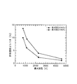
図14に、各耐圧クラス(740V、1100V、2300V、4500V)における耐圧と並列pn接合層の濃度との関係を示す。図14において、縦軸は最大耐圧BVmaxを1としたときの耐圧比であり、横軸は最大耐圧BVmaxが得られるときの濃度を1としたときの濃度比である。図14より、最大耐圧が大きくなる、すなわち高耐圧化するのに伴って、濃度のばらつきに対する耐圧低下の程度が急激になっていることがわかる。
【0017】
図15に、最大耐圧の90%および95%の耐圧を得るために許容される濃度ばらつきと最大耐圧との関係を示す。図15において、縦軸は許容濃度ばらつき[%]であり、横軸は最大耐圧[V]である。図15より、最大耐圧が大きくなるのに伴って、許容濃度ばらつきが急激に小さくなっていることがわかる。
【0018】
図15に示す通り、たとえば通常で13%の濃度ばらつきがあると仮定すると、740Vクラスでは最大耐圧の90%以上の耐圧が得られる。それに対して、2300Vクラスで耐圧を最大耐圧の95%以上にするためには濃度のばらつきを2%程度にする必要である。また、4500Vクラスでは、最大耐圧の95%以上の耐圧を得るには濃度のばらつきを1%程度に抑える必要がある。
【0019】
上述したようにイオンビームの衝突回数は濃度ばらつきの原因であり、衝突回数が1/10になれば濃度のばらつきも1/10になるため、通常の濃度ばらつき13%に対して、λ=10dにセッティングすることによって濃度ばらつきを1.3%に抑えることが可能となる。さらに、λ=100dとすれば0.13%の濃度ばらつきに抑えることが可能となる。したがって、本実施の形態ではλ≧10dである。
【0020】
ところで、イオンビームの平均自由工程λはチャンバー内圧力の影響を受ける。チャンバー内に存在する分子の密度をn[cm-3]、チャンバー内圧力をp[Torr]、絶対温度をT[K]とすると、気体運動論によればつぎの(1)式が成り立つ。
【0021】
p=1×10-19nT ・・・(1)
【0022】
また、リンの原子半径をr1[cm]、ソースガス分子の分子半径をr2[cm]とすると、平均自由工程λ[cm]はつぎの(2)式で表される。
【0023】
λ=1/(21/2π(r1+r2)2n) ・・・(2)
【0024】
上記(1)式および(2)式よりnを消去すると、つぎの(3)式が得られる。
【0025】
λ=1/(21/2π(r1+r2)2)×1×10-19T/p ・・・(3)
【0026】
ここで説明を簡単にするため、r1およびr2を1×10⁻⁸[cm]と仮定すると、つぎの(4)式が得られる。圧力の単位がPaの場合は(5)式となる。
【0027】
λ=2.25×10⁻⁴T/p ・・・(4)
λ=3.00×10⁻²T/p ・・・(5)
【0028】
たとえば、イオンビーム照射時のチャンバー内圧力が10-2Paの場合には、平均自由工程λは4000cmとなる。比較として、前記特開2001−168036号公報による従来技術において、チャンバー内圧力を1mTorrとすると平均自由工程λは300cmとなる。イオンビーム銃とエピタキシャル基板との間の距離dを300cmとすれば、従来はエピタキシャル基板にイオンビームが到達する以前に必ず衝突が起こることになる。
【0029】
それに対して、本実施の形態においてチャンバー内圧力を10-2Paとすれば、衝突回数は300/4000回、すなわち0.075回である。したがって、本実施の形態においてチャンバー内圧力を10-2Paとすることによって、濃度のばらつきを1/0.075=13.3倍抑えることができる。換言すれば、前記特開2001−168036号公報による従来技術による13.3%の濃度ばらつきを1%に抑えることができる。
【0030】
また、望ましくはイオンビーム照射時のチャンバー内圧力は10-3Paであるとよく、さらに望ましくは10-4Paであるとよい。その場合には、濃度ばらつきをそれぞれ0.1%および0.01%に抑えることが可能となり、事実上ばらつきがないものとすることができる。また、10-4Pa以下の圧力であれば、イオン電荷の中性化も回避される。また、最大耐圧4500V以上の高耐圧クラスにおいてもばらつきの低減が可能となる。
【0031】
つぎに、ボロンおよびリン照射用のイオンビーム銃を備えた枚葉式のエピタキシャル成長炉を用いた場合の超接合基板の製造方法について説明する。図2〜図5は、図1の枚葉式のエピタキシャル成長炉による、超接合基板の製造工程を順に示す模式図である。
【0032】
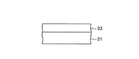
まず、チャンバー3内において、ソースガス導入口1よりSiCl4などのソースガスを導入して、n型の低抵抗半導体基板よりなる低抵抗層31の上に、低濃度(1×1013cm-3程度)のn-高比抵抗層32を約8μmの厚さで成膜する(図2)。エピタキシャル成長中のチャンバー内圧力はおおむね100〜3000Paの範囲であり、特に限定しないが、たとえば本実施の形態では400Paとする。たとえばMOSFETの場合、低抵抗層31はn+ドレイン層となる。
【0033】
引きつづき、そのままの状態、すなわちチャンバー3内にエピタキシャル基板8を入れたまま、チャンバー3内のソースガスを排気口2より排気して、イオンビームが散乱しにくい圧力まで真空度を高めた後、選択的にボロンとリンのイオンビーム照射をおこない、n-高比抵抗層32の表面にボロンビーム照射領域34とリンビーム照射領域35を交互に設ける(図3)。イオンビーム照射時のチャンバー内圧力は上述したように10-2Pa以下であるのが適当であるが、本実施の形態では、イオン電荷の中性化を実質的になくすため、特に限定しないが、たとえば10-6Paとする。
【0034】
また、このとき、リンの注入量とボロンの注入量は等しいことが望ましい。これは、最終的にリンビーム照射領域35がnドリフト領域となり、ボロンビーム照射領域34がp仕切り領域となったときに、両者の空乏層の広がりが同じになるからである。また、リンビーム照射領域35およびボロンビーム照射領域34の幅は等しくすることが望ましい。本実施の形態ではリンビーム照射領域35およびボロンビーム照射領域34の幅はたとえば3μmであり、リンおよびボロンの各注入量はたとえば3.6×1013cm-2である。
【0035】
イオンビーム照射後、そのままの状態で再びチャンバー3内にソースガスを導入し、再度上述した要領でエピタキシャル成長をおこない、n-高抵抗層32を形成する。その後、再び上述した要領でチャンバー3内を減圧し、リンおよびボロンのイオンビーム照射をおこなう。このようにエピタキシャル基板8をチャンバー3内に入れたまま、エピタキシャル成長とイオンビーム照射を複数回繰り返し、並列pn接合層を所定の厚さにする。特に限定しないが、本実施の形態では、エピタキシャル成長とイオンビーム照射の工程をたとえば6回繰り返しおこなう。
【0036】
その後、基板表面に上述した要領で高比抵抗層32をエピタキシャル法により約4μm成長させる(図4)。これにより、エピタキシャル成長によって形成された熱処理前の並列pn接合層の厚さは、たとえば52μmとなる。この後、エピタキシャル基板8をチャンバー3内から取り出し、熱処理をおこない、注入された不純物を拡散させて並列pn接合層のp仕切り領域36とnドリフト領域37を形成する(図5)。
【0037】
本実施の形態では、1150℃で10時間の熱処理により、nドリフト領域37とp仕切り領域36とが接続し、各nドリフト領域37および各p仕切り領域36の幅は6μmとなり、並列pn接合層としては12μmとなる。なお、ビーム照射幅や不純物のドーズ量や熱処理時間等を変えることによって、最終的な並列pn接合層のnドリフト領域37とp仕切り領域36の条件は変更可能である。
【0038】
上述したように、実施の形態1によれば、同一チャンバー3内でエピタキシャル成長と、エピタキシャル成長時よりも低い圧力でのイオンビーム照射とを交互に繰り返しおこなうことによって、簡易に量産性よく並列pn接合層が製造される。したがって、ばらつきの小さい超接合半導体素子を簡易に量産性よく製造することができる。なお、多数のイオンビーム銃を並列に、かつ等間隔で配置するようにしても、nドリフト領域37とp仕切り領域36の幅を等しくすることができる。この場合には、イオン注入用のレジストマスクを形成する必要がない。つまり、フォトリソグラフィーをおこなわずに並列pn接合層を形成することができる。
【0039】
実施の形態2.
図6は実施の形態2において用いられる枚葉式のエピタキシャル成長炉の断面模式図である。このエピタキシャル成長炉では、ソースガス導入口1およびソースガス排気口2を備えたチャンバー3に、ボロン照射用イオンビーム銃4を複数備えている。リン照射用イオンビーム銃は設けられていない。また、サセプタ6を加熱するために、RFコイル7がサセプタ6の直下に敷設され、エピタキシャル基板8はサセプタ6の上に設置される。
【0040】
なお、ボロン照射用イオンビーム銃4とエピタキシャル基板8との間の距離dと、イオンビームの平均自由工程λとの関係や、イオンビーム照射時のチャンバー内圧力などは実施の形態1と同じである。したがって、説明を省略する。
【0041】
つぎに、ボロン照射用のイオンビーム銃のみを備えた枚葉式のエピタキシャル成長炉を用いた場合の超接合基板の製造方法について説明する。図7〜図9は、図6の枚葉式のエピタキシャル成長炉による、超接合基板の製造工程を順に示す模式図である。
【0042】
まず、チャンバー3内において、n型の低抵抗半導体基板よりなる低抵抗層31の上に、不純物濃度が3.6×1015cm-3程度のn型半導体層33を約8μmの厚さで成膜する(図7)。エピタキシャル成長中のチャンバー内圧力はおおむね100〜3000Paの範囲である。
【0043】
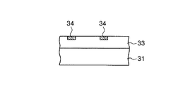
引きつづき、チャンバー3内にエピタキシャル基板8を入れたまま、チャンバー3内を10-2Pa以下、たとえば10-6Paまで排気して、ボロンのイオンビーム照射によりn型半導体層33の表面にボロンビーム照射領域34を選択的に設ける(図8)。本実施の形態では、ボロンビーム照射領域34の幅はたとえば3μmであり、ボロンの注入量はたとえば1.2×1013cm-2である。
【0044】
実施の形態1と同様に、エピタキシャル基板8をチャンバー3内に入れたまま、エピタキシャル成長とイオンビーム照射を複数回繰り返し、並列pn接合層を所定の厚さにする。特に限定しないが、本実施の形態では、エピタキシャル成長とイオンビーム照射の工程をたとえば6回繰り返しおこなう。その後、基板表面に、不純物濃度が3.6×1015cm-3程度の低濃度n型半導体層33をエピタキシャル法により約4μm成長させる(図9)。
【0045】
この後、エピタキシャル基板8をチャンバー3内から取り出し、熱処理をおこない、注入されたボロンを拡散させて並列pn接合層のp仕切り領域36およびnドリフト領域37を形成する(図5)。nドリフト領域37は、エピタキシャル成長したn型半導体層33である。本実施の形態では、1150℃で10時間の熱処理により、6μm幅のnドリフト領域37と6μm幅のp仕切り領域36とが接続し、並列pn接合層としては12μmとなる。なお、ビーム照射幅や不純物のドーズ量や熱処理時間等を変えることによって、最終的な並列pn接合層のnドリフト領域37とp仕切り領域36の条件は変更可能である。
【0046】
上述したように、実施の形態2によれば、実施の形態1と同様に、簡易に量産性よく並列pn接合層が製造されるので、ばらつきの小さい超接合半導体素子を簡易に量産性よく製造することができる。なお、実施の形態2の方法は、p型低抵抗半導体基板上にp型半導体層を形成し、選択的にリンを注入する場合にも適用可能である。この場合には、複数のリン照射用イオンビーム銃を備えた枚葉式のエピタキシャル成長炉を用いることが有効である。
【0047】
実施の形態3.
図10は実施の形態3において用いられる枚葉式のエピタキシャル成長炉の断面模式図である。このエピタキシャル成長炉では、ソースガス導入口1およびソースガス排気口2を備えたチャンバー3に、ボロン照射用イオンビーム銃4とリン照射用イオンビーム銃5を各1台ずつ備えている。また、サセプタ6を加熱するために、RFコイル7がサセプタ6の直下に敷設され、エピタキシャル基板8はサセプタ6の上に設置される。
【0048】
なお、イオンビーム銃4,5とエピタキシャル基板8との間の距離dと、イオンビームの平均自由工程λとの関係や、イオンビーム照射時のチャンバー内圧力などは実施の形態1と同じである。したがって、説明を省略する。
【0049】
図10に示す構成のエピタキシャル成長炉を用いた場合には、ボロン照射用イオンビーム銃4およびリン照射用イオンビーム銃5が各1台ずつしかない。そのため、実施の形態3では、これら1台ずつのイオンビーム銃4,5を走査することにより、並列pn接合層を形成する。製造方法のその他の点については実施の形態1と同じである。実施の形態3によれば、ボロン照射用とリン照射用のイオンビーム銃4,5が1台ずつであるため、エピタキシャル成長炉のコストを低く抑えることができる。
【0050】
実施の形態4.
実施の形態4で使用されるエピタキシャル成長炉は基本的に図10に示す構成と同じである。また、イオンビーム銃4,5とエピタキシャル基板8との間の距離dと、イオンビームの平均自由工程λとの関係や、イオンビーム照射時のチャンバー内圧力などは実施の形態1と同じである。したがって、重複する説明を省略する。
【0051】
図11〜図13は、実施の形態第4にかかる製造方法による超接合基板の製造工程を順に示す模式図である。まず、チャンバー3内において、n型の低抵抗半導体基板よりなる低抵抗層31の上に、低濃度(1×1013cm-3程度)のn-高比抵抗層32を約8μmの厚さで成膜する(図11)。エピタキシャル成長中のチャンバー内圧力はおおむね100〜3000Paの範囲である。
【0052】
引きつづき、チャンバー3内にエピタキシャル基板8を入れたまま、チャンバー3内を10-2Pa以下、たとえば10-6Paまで排気して、ボロンおよびリンのイオンビーム照射をおこなう。このとき、ピッチが広い並列pn接合層を形成する領域に対しては、ビーム径を太くして走査し、一方、ピッチが狭い並列pn接合層を形成する領域に対してはビーム径を細くして走査する。
【0053】
このようにすることによって、図11に示すように、ピッチが広いボロンビーム照射領域34およびリンビーム照射領域35と、ピッチが狭いボロンビーム照射領域38およびリンビーム照射領域39が形成される。本実施の形態では、特に限定しないが、たとえばピッチが広い領域でのビーム銃の走査をビーム径3μmでおこない、狭いピッチの領域ではビーム径を1.5μmとして走査する。
【0054】
実施の形態1と同様に、エピタキシャル基板8をチャンバー3内に入れたまま、エピタキシャル成長とイオンビーム照射を複数回、たとえば6回繰り返し、並列pn接合層を所定の厚さにする。その後、基板表面に高比抵抗層32をエピタキシャル法により約4μm成長させる(図12)。そして、エピタキシャル基板8をチャンバー3内から取り出し、熱処理をおこない、注入された不純物を拡散させて幅が広い並列pn接合層のp仕切り領域36およびnドリフト領域37と、幅が狭い並列pn接合層のp仕切り領域40およびnドリフト領域41を形成する(図13)。
【0055】
実施の形態4によれば、狭いピッチの並列pn接合層では、最終的な熱処理による相互拡散によって濃度が低くなり、電界が緩和されやすくなるため、耐圧が向上する。したがって、狭いピッチの並列pn接合層を耐圧構造部などに配置することが可能となる。なお、エピタキシャル成長炉を、ボロンおよびリンのそれぞれに対してビーム径が太いイオンビーム銃とビーム径が細いイオンビーム銃とをそれぞれ1台以上ずつ備えた構成としても同様の効果が得られる。
【0056】
【発明の効果】
本発明によれば、エピタキシャル成長時のチャンバー内圧力よりも低い圧力でイオンビームが照射されるため、イオンビームの散乱が抑制され、不純物濃度のばらつきの小さい並列pn接合層が形成される。したがって、ばらつきの小さい超接合半導体素子を簡易に量産性よく製造することができる。
【図面の簡単な説明】
【図1】本発明の実施の形態1におけるボロンおよびリン照射用の複数のビーム銃を備えた枚葉式のエピタキシャル成長炉の断面模式図である。
【図2】図1の枚葉式のエピタキシャル成長炉により製造される超接合基板の製造段階における構成を示す断面模式図である。
【図3】図1の枚葉式のエピタキシャル成長炉により製造される超接合基板の製造段階における構成を示す断面模式図である。
【図4】図1の枚葉式のエピタキシャル成長炉により製造される超接合基板の製造段階における構成を示す断面模式図である。
【図5】図1の枚葉式のエピタキシャル成長炉により製造される超接合基板の製造段階における構成を示す断面模式図である。
【図6】本発明の実施の形態2における複数のボロン照射用のビーム銃を備えた枚葉式のエピタキシャル成長炉の断面模式図である。
【図7】図6の枚葉式のエピタキシャル成長炉により製造される超接合基板の製造段階における構成を示す断面模式図である。
【図8】図6の枚葉式のエピタキシャル成長炉により製造される超接合基板の製造段階における構成を示す断面模式図である。
【図9】図6の枚葉式のエピタキシャル成長炉により製造される超接合基板の製造段階における構成を示す断面模式図である。
【図10】本発明の実施の形態3におけるボロン照射用のビーム銃とリン照射用のビーム銃とを各1台備えた枚葉式のエピタキシャル成長炉の断面模式図である。
【図11】本発明の実施の形態3にかかる製造方法により製造される超接合基板の製造段階における構成を示す断面模式図である。
【図12】本発明の実施の形態3にかかる製造方法により製造される超接合基板の製造段階における構成を示す断面模式図である。
【図13】本発明の実施の形態3にかかる製造方法により製造される超接合基板の製造段階における構成を示す断面模式図である。
【図14】耐圧クラス740V、1100V、2300V、4500Vにおける耐圧と並列pn接合層の濃度との関係を規格化して示す特性図である。
【図15】最大耐圧の90%および95%における許容濃度ばらつきと最大耐圧との関係を示す特性図である。
【符号の説明】
1 ソースガス導入口
2 ソースガス排気口
3 チャンバー
4 ボロン照射用イオンビーム銃
5 リン照射用イオンビーム銃
8 エピタキシャル基板
31 低抵抗層
32 高比抵抗層
33 n型半導体層
34,38 ボロンビーム照射領域
35,39 リンビーム照射領域
36,40 p仕切り領域
37,41 nドリフト領域[0001]
BACKGROUND OF THE INVENTION
The present invention relates to a method of manufacturing a superjunction semiconductor device capable of achieving both high breakdown voltage and large current capacity, and in particular, a MOSFET (insulated gate field effect transistor) and IGBT (insulated gate type) having a parallel pn junction layer. The present invention relates to a method of manufacturing a superjunction semiconductor device such as a bipolar transistor) or a bipolar transistor or a diode.
[0002]
[Prior art]
The conventional high voltage semiconductor element has a high resistivity drift region in the main current path in order to obtain a high breakdown voltage. Therefore, the higher the withstand voltage, the larger the voltage drop in this part and the higher the on-voltage. was there. As a solution to this problem, the drift layer is composed of a parallel pn layer in which n-type regions and p-type regions having an increased impurity concentration are alternately stacked, and is depleted and bears a breakdown voltage in the off state. A semiconductor device having such a structure is disclosed in, for example, US Pat. No. 5,216,275.
[0003]
Here, as described above, the parallel pn junction layer is a structure in which a first conductivity type (for example, n-type) drift region and a second conductivity type (for example, p-type) partition region are alternately and repeatedly bonded. That is. A superjunction semiconductor element is a semiconductor element having a drift region composed of a parallel pn junction layer that conducts a current in an on state and is depleted in an off state.
[0004]
Conventionally, as a method of forming a parallel pn junction layer, a method of filling a trench structure by epitaxial growth is known. However, this method has a problem in that the substrate has a non-removable damage when forming the trench because the trench has a high aspect ratio. There is also a problem that it is extremely difficult to fill the trench with a high-quality epitaxial layer.
[0005]
Therefore, the present inventors selectively implant ions by irradiating the epitaxial growth layer with an ion beam of n-type impurities and p-type impurities while epitaxially growing a high-resistance semiconductor layer on a low-resistance semiconductor substrate. Have previously filed a method for forming a parallel pn junction layer (Japanese Patent Laid-Open No. 2001-168036). According to this method, it is possible to easily form a parallel pn junction layer.
[0006]
[Problems to be solved by the invention]
However, according to the subsequent studies by the inventors, in the method for forming a parallel pn junction layer according to the above-mentioned Japanese Patent Application Laid-Open No. 2001-168036, the chamber internal pressure during epitaxial growth is relatively high as 100 to 3000 Pa by supplying the source gas, It was found that since the degree of vacuum is low, the ion beam is likely to be scattered, and the impurity concentration of the parallel pn junction layer may vary.
[0007]
The present invention has been made in view of the above-described circumstances, and is capable of manufacturing a superjunction semiconductor element having a parallel pn junction layer with small variations in impurity concentration and capable of easily manufacturing the superjunction semiconductor element with high productivity. It aims to provide a method.
[0008]
[Means for Solving the Problems]
In order to achieve the above object, the present invention provides a low resistance layer between the first main surface and the second main surface, current flows in the on state, and p-type regions and n-type regions alternate. And a method of epitaxially growing a high resistivity layer having a resistance higher than that of the low resistance layer on a surface of the low resistance layer in a method of manufacturing a super junction semiconductor device including a parallel pn junction layer having a configuration arranged in Following the epitaxial growth step, in the same chamber, with the pressure in the chamber being lower than that during epitaxial growth, a step of selectively injecting a predetermined impurity into the high resistivity layer by ion beam irradiation; And a step of diffusing the implanted impurities by heat treatment to form the parallel pn junction layer. According to the present invention, since the ion beam is irradiated at a pressure lower than the pressure in the chamber at the time of epitaxial growth, scattering of the ion beam is suppressed, and a parallel pn junction layer having a small variation in impurity concentration is formed.
[0009]
In the present invention, the heat treatment may be performed after the epitaxial growth and the ion beam irradiation are repeatedly performed. In this way, a parallel pn junction layer having a desired thickness is formed.
[0010]
In the present invention, the pressure in the chamber at the time of ion beam irradiation is 1 × 10. -2 It is good also as Pa or less. In this case, the ion beam is less likely to be scattered, and variations in the impurity concentration of the parallel pn junction layer are suppressed.
[0011]
In the present invention, the ion species at the time of ion beam irradiation may be boron, phosphorus, or a combination of boron and phosphorus. According to this configuration, for example, a p-type region is formed by boron implantation, and an n-type region is formed by phosphorus implantation.
[0012]
Moreover, in this invention, it is good also as a structure which forms a parallel pn junction layer of a different width | variety by changing a beam diameter at the time of the said ion beam irradiation. In this way, parallel pn junction layers having different pitches are formed, and in the narrow pitch parallel pn junction layers, the impurity concentration becomes low due to mutual diffusion during heat treatment, and the electric field is easily relaxed. The breakdown voltage is improved.
[0013]
In the present invention, the mean free path of the ion beam may be 10 times or more the distance between the ion beam gun and the semiconductor element. In this case, the ion beam is less likely to be scattered, and variations in the impurity concentration of the parallel pn junction layer are suppressed.
[0014]
DETAILED DESCRIPTION OF THE INVENTION
Hereinafter, embodiments of the present invention will be described with reference to the drawings.
FIG. 1 is a schematic cross-sectional view of a single wafer epitaxial growth furnace used in the first embodiment. In this epitaxial growth furnace, a plurality of boron irradiation
[0015]
Here, the distance d between the
[0016]
FIG. 14 shows the relationship between the breakdown voltage and the concentration of the parallel pn junction layer in each breakdown voltage class (740 V, 1100 V, 2300 V, 4500 V). In FIG. 14, the vertical axis represents the breakdown voltage ratio when the maximum breakdown voltage BVmax is 1, and the horizontal axis represents the concentration ratio when the density at which the maximum breakdown voltage BVmax is obtained is 1. From FIG. 14, it can be seen that as the maximum withstand voltage increases, that is, the withstand voltage increases, the degree of withstand voltage decrease with respect to the concentration variation becomes abrupt.
[0017]
FIG. 15 shows the relationship between the variation in concentration allowed to obtain 90% and 95% of the maximum breakdown voltage and the maximum breakdown voltage. In FIG. 15, the vertical axis represents the allowable density variation [%], and the horizontal axis represents the maximum breakdown voltage [V]. From FIG. 15, it can be seen that as the maximum withstand voltage increases, the allowable concentration variation decreases rapidly.
[0018]
As shown in FIG. 15, for example, assuming that there is a normal concentration variation of 13%, a breakdown voltage of 90% or more of the maximum breakdown voltage can be obtained in the 740V class. On the other hand, in order to increase the breakdown voltage to 95% or more of the maximum breakdown voltage in the 2300V class, the concentration variation needs to be about 2%. Further, in the 4500 V class, in order to obtain a breakdown voltage of 95% or more of the maximum breakdown voltage, it is necessary to suppress variation in concentration to about 1%.
[0019]
As described above, the number of collisions of the ion beam is a cause of density variation, and if the number of collisions becomes 1/10, the density variation also becomes 1/10. Therefore, for a normal density variation of 13%, λ = 10d By setting to, the density variation can be suppressed to 1.3%. Furthermore, if λ = 100d, it is possible to suppress the density variation to 0.13%. Therefore, in this embodiment, λ ≧ 10d.
[0020]
By the way, the mean free path λ of the ion beam is affected by the pressure in the chamber. The density of the molecules present in the chamber is n [cm -3 If the pressure in the chamber is p [Torr] and the absolute temperature is T [K], the following equation (1) holds according to the gas kinetic theory.
[0021]
p = 1 × 10 -19 nT (1)
[0022]
If the atomic radius of phosphorus is r1 [cm] and the molecular radius of the source gas molecule is r2 [cm], the mean free path λ [cm] is expressed by the following equation (2).
[0023]
λ = 1 / (2 1/2 π (r1 + r2) 2 n) (2)
[0024]
When n is eliminated from the above equations (1) and (2), the following equation (3) is obtained.
[0025]
λ = 1 / (2 1/2 π (r1 + r2) 2 ) × 1 × 10 -19 T / p (3)
[0026]
For simplicity of explanation, r1 and r2 are set to 1 × 10. -8 Assuming [cm], the following equation (4) is obtained. When the unit of pressure is Pa, equation (5) is obtained.
[0027]
λ = 2.25 × 10 -Four T / p (4)
λ = 3.00 × 10 -2 T / p (5)
[0028]
For example, the pressure in the chamber at the time of ion beam irradiation is 10 -2 In the case of Pa, the mean free path λ is 4000 cm. For comparison, in the prior art disclosed in Japanese Patent Laid-Open No. 2001-168036, when the pressure in the chamber is 1 mTorr, the mean free path λ is 300 cm. If the distance d between the ion beam gun and the epitaxial substrate is 300 cm, conventionally, collisions always occur before the ion beam reaches the epitaxial substrate.
[0029]
On the other hand, in this embodiment, the pressure in the chamber is set to 10 -2 Assuming Pa, the number of collisions is 300/4000, that is, 0.075. Therefore, in this embodiment, the pressure in the chamber is set to 10 -2 By setting it as Pa, the dispersion | variation in a density | concentration can be suppressed 1 / 0.075 = 13.3 times. In other words, the 13.3% density variation according to the prior art disclosed in Japanese Patent Laid-Open No. 2001-168036 can be suppressed to 1%.
[0030]
Desirably, the pressure in the chamber during ion beam irradiation is 10 -3 It is good that it is Pa, more preferably 10 -Four It is good that it is Pa. In that case, the density variation can be suppressed to 0.1% and 0.01%, respectively, and the variation can be virtually eliminated. 10 -Four If the pressure is less than or equal to Pa, neutralization of ionic charge is also avoided. Further, variation can be reduced even in a high withstand voltage class having a maximum withstand voltage of 4500 V or more.
[0031]
Next, a method of manufacturing a super-junction substrate when using a single wafer type epitaxial growth furnace equipped with an ion beam gun for boron and phosphorus irradiation will be described. 2 to 5 are schematic views sequentially showing the manufacturing process of the super-junction substrate by the single wafer type epitaxial growth furnace of FIG.
[0032]
First, in the
[0033]
Subsequently, after the source gas in the
[0034]
At this time, it is desirable that the injection amount of phosphorus and the injection amount of boron are equal. This is because when the phosphorus
[0035]
After the ion beam irradiation, the source gas is again introduced into the
[0036]
Thereafter, the
[0037]
In the present embodiment, the
[0038]
As described above, according to the first embodiment, the parallel pn junction layer can be easily and efficiently mass-produced by alternately repeating epitaxial growth and ion beam irradiation at a lower pressure than that during epitaxial growth in the
[0039]
FIG. 6 is a schematic sectional view of a single wafer type epitaxial growth furnace used in the second embodiment. In this epitaxial growth furnace, a plurality of boron irradiation
[0040]
The relationship between the distance d between the ion beam gun for
[0041]
Next, a method for manufacturing a super-junction substrate when using a single-wafer epitaxial growth furnace equipped with only an ion beam gun for boron irradiation will be described. 7 to 9 are schematic views sequentially showing the manufacturing process of the super junction substrate by the single wafer type epitaxial growth furnace of FIG.
[0042]
First, in the
[0043]
Subsequently, while the epitaxial substrate 8 is put in the
[0044]
Similar to the first embodiment, the epitaxial growth and the ion beam irradiation are repeated a plurality of times while the epitaxial substrate 8 is placed in the
[0045]
Thereafter, the epitaxial substrate 8 is taken out from the
[0046]
As described above, according to the second embodiment, as in the first embodiment, the parallel pn junction layer is easily manufactured with high mass productivity. Therefore, a superjunction semiconductor element with small variations can be easily manufactured with high mass productivity. can do. Note that the method of
[0047]
FIG. 10 is a schematic sectional view of a single wafer type epitaxial growth furnace used in the third embodiment. In this epitaxial growth furnace, one
[0048]
The relationship between the distance d between the
[0049]
When the epitaxial growth furnace having the configuration shown in FIG. 10 is used, there is only one boron irradiation
[0050]
The epitaxial growth furnace used in the fourth embodiment is basically the same as that shown in FIG. The relationship between the distance d between the
[0051]
FIG. 11 to FIG. 13 are schematic views sequentially illustrating the manufacturing process of the super-bonded substrate by the manufacturing method according to the fourth embodiment. First, in the
[0052]
Subsequently, while the epitaxial substrate 8 is put in the
[0053]
By doing so, as shown in FIG. 11, a boron
[0054]
Similar to the first embodiment, while the epitaxial substrate 8 is placed in the
[0055]
According to the fourth embodiment, in the parallel pn junction layer with a narrow pitch, the concentration decreases due to the interdiffusion by the final heat treatment, and the electric field is easily relaxed, so that the breakdown voltage is improved. Therefore, it becomes possible to arrange parallel pn junction layers with a narrow pitch in the breakdown voltage structure. The same effect can be obtained even if the epitaxial growth furnace is provided with at least one ion beam gun having a large beam diameter and one ion beam gun having a small beam diameter for each of boron and phosphorus.
[0056]
【The invention's effect】
According to the present invention, since the ion beam is irradiated at a pressure lower than the pressure in the chamber at the time of epitaxial growth, scattering of the ion beam is suppressed, and a parallel pn junction layer having a small variation in impurity concentration is formed. Therefore, a superjunction semiconductor element with small variation can be easily manufactured with high productivity.
[Brief description of the drawings]
FIG. 1 is a schematic cross-sectional view of a single-wafer type epitaxial growth furnace provided with a plurality of beam guns for boron and phosphorus irradiation in
2 is a schematic cross-sectional view showing a configuration of a super-junction substrate manufactured by the single wafer epitaxial growth furnace of FIG. 1 in a manufacturing stage.
3 is a schematic cross-sectional view showing a configuration of a super-junction substrate manufactured by the single wafer epitaxial growth furnace of FIG. 1 in a manufacturing stage.
4 is a schematic cross-sectional view showing a configuration of a super-junction substrate manufactured by the single-wafer epitaxial growth furnace of FIG. 1 in a manufacturing stage.
5 is a schematic cross-sectional view showing a configuration of a super-junction substrate manufactured by the single-wafer epitaxial growth furnace of FIG. 1 in a manufacturing stage.
FIG. 6 is a schematic cross-sectional view of a single wafer epitaxial growth furnace provided with a plurality of boron irradiation beam guns according to a second embodiment of the present invention.
7 is a schematic cross-sectional view showing a configuration of a super-junction substrate manufactured by the single wafer epitaxial growth furnace of FIG. 6 in a manufacturing stage.
8 is a schematic cross-sectional view showing a configuration of a super-junction substrate manufactured by the single wafer epitaxial growth furnace of FIG. 6 in a manufacturing stage.
9 is a schematic cross-sectional view showing a configuration of a super-junction substrate manufactured by the single-wafer epitaxial growth furnace of FIG. 6 in a manufacturing stage.
FIG. 10 is a schematic cross-sectional view of a single-wafer epitaxial growth furnace provided with one boron irradiation beam gun and one phosphorus irradiation beam gun in
FIG. 11 is a schematic cross-sectional view showing a configuration in a manufacturing stage of a superjunction substrate manufactured by the manufacturing method according to the third embodiment of the present invention.
FIG. 12 is a schematic cross-sectional view showing a configuration in a manufacturing stage of a superjunction substrate manufactured by the manufacturing method according to the third embodiment of the present invention.
FIG. 13 is a schematic cross-sectional view showing a configuration in a manufacturing stage of a superjunction substrate manufactured by the manufacturing method according to the third embodiment of the present invention.
FIG. 14 is a characteristic diagram showing a normalized relationship between the withstand voltage in the withstand
FIG. 15 is a characteristic diagram showing the relationship between the allowable concentration variation and the maximum breakdown voltage at 90% and 95% of the maximum breakdown voltage.
[Explanation of symbols]
1 Source gas inlet
2 Source gas exhaust port
3 Chamber
4 Ion beam gun for boron irradiation
5 Ion beam gun for phosphorus irradiation
8 Epitaxial substrate
31 Low resistance layer
32 High resistivity layer
33 n-type semiconductor layer
34,38 Boron beam irradiation area
35, 39 Phosphorus beam irradiation area
36, 40 p partition area
37, 41 n drift region
Claims (6)
前記低抵抗層の表面に前記低抵抗層よりも抵抗の大きい高比抵抗層をエピタキシャル成長させる工程と、
前記エピタキシャル成長工程につづいて同一チャンバー内で、チャンバー内圧力がエピタキシャル成長時よりも低い状態で、前記高比抵抗層に所定の不純物をイオンビーム照射により選択的に注入する工程と、
前記高比抵抗層に注入された不純物を熱処理により拡散させて前記並列pn接合層を形成する工程と、
を含むことを特徴とする超接合半導体素子の製造方法。A low-resistance layer between the first main surface and the second main surface, a parallel pn junction layer having a configuration in which a current flows in an on state and p-type regions and n-type regions are alternately arranged; In a method of manufacturing a superjunction semiconductor device comprising:
Epitaxially growing a high specific resistance layer having a higher resistance than the low resistance layer on the surface of the low resistance layer;
In the same chamber following the epitaxial growth step, with the pressure in the chamber being lower than that during epitaxial growth, a step of selectively injecting a predetermined impurity into the high resistivity layer by ion beam irradiation;
A step of diffusing impurities injected into the high resistivity layer by heat treatment to form the parallel pn junction layer;
The manufacturing method of the super junction semiconductor element characterized by the above-mentioned.
Priority Applications (1)
| Application Number | Priority Date | Filing Date | Title |
|---|---|---|---|
| JP2002064409A JP3849552B2 (en) | 2002-03-08 | 2002-03-08 | Superjunction semiconductor device manufacturing method |
Applications Claiming Priority (1)
| Application Number | Priority Date | Filing Date | Title |
|---|---|---|---|
| JP2002064409A JP3849552B2 (en) | 2002-03-08 | 2002-03-08 | Superjunction semiconductor device manufacturing method |
Publications (2)
| Publication Number | Publication Date |
|---|---|
| JP2003264286A JP2003264286A (en) | 2003-09-19 |
| JP3849552B2 true JP3849552B2 (en) | 2006-11-22 |
Family
ID=29197218
Family Applications (1)
| Application Number | Title | Priority Date | Filing Date |
|---|---|---|---|
| JP2002064409A Expired - Fee Related JP3849552B2 (en) | 2002-03-08 | 2002-03-08 | Superjunction semiconductor device manufacturing method |
Country Status (1)
| Country | Link |
|---|---|
| JP (1) | JP3849552B2 (en) |
Families Citing this family (3)
| Publication number | Priority date | Publication date | Assignee | Title |
|---|---|---|---|---|
| KR101818730B1 (en) * | 2011-08-31 | 2018-01-16 | 주식회사 원익아이피에스 | Substrate processing apparatus, substrate processing system, and substrate processing method |
| CN104992963B (en) * | 2015-07-24 | 2018-01-02 | 杭州士兰微电子股份有限公司 | The semiconductor devices and its manufacture method of super-junction structure, reticle |
| JP7135422B2 (en) | 2018-05-11 | 2022-09-13 | 富士電機株式会社 | Semiconductor device manufacturing method |
-
2002
- 2002-03-08 JP JP2002064409A patent/JP3849552B2/en not_active Expired - Fee Related
Also Published As
| Publication number | Publication date |
|---|---|
| JP2003264286A (en) | 2003-09-19 |
Similar Documents
| Publication | Publication Date | Title |
|---|---|---|
| US11515387B2 (en) | Method of manufacturing silicon carbide semiconductor device, method of manufacturing silicon carbide substrate, and silicon carbide substrate | |
| US20250267902A1 (en) | Superjunction silicon carbide semiconductor device having parallel pn column structure with crystal defects | |
| US11393812B2 (en) | Semiconductor device and method of manufacturing semiconductor device | |
| JP6237921B2 (en) | Semiconductor device and manufacturing method of semiconductor device | |
| US9324857B2 (en) | Semiconductor device manufacturing method | |
| US11355595B2 (en) | Semiconductor device and method of manufacturing semiconductor device | |
| JP5985789B2 (en) | Manufacturing method of super junction semiconductor device | |
| JP2009004668A (en) | Semiconductor device | |
| JP2011505709A (en) | Method of manufacturing a power semiconductor device having a voltage maintaining layer with a trapezoidal trench for forming a floating island | |
| EP1453105A2 (en) | Vertical field effect transistor having a high withstand voltage | |
| US12224320B2 (en) | Silicon carbide semiconductor device and method of manufacturing silicon carbide semiconductor device | |
| US20120286324A1 (en) | Manufacturing method for insulated-gate bipolar transitor and device using the same | |
| JP2011192823A (en) | Method of manufacturing superjunction semiconductor device | |
| US10424637B2 (en) | Method of manufacturing semiconductor device | |
| US20240234496A1 (en) | Method of manufacturing silicon carbide semiconductor device | |
| CN102347364B (en) | There is the semiconductor device of drift region and compensatory zone | |
| JP3849552B2 (en) | Superjunction semiconductor device manufacturing method | |
| JP2024153517A (en) | Super-junction silicon carbide semiconductor device and method for manufacturing the super-junction silicon carbide semiconductor device | |
| JP2022503888A (en) | Masking systems and methods during high energy injection when manufacturing wide bandgap semiconductor devices | |
| JP2004221370A (en) | Semiconductor device | |
| US20230246076A1 (en) | Silicon carbide semiconductor device and method of manufacturing silicon carbide semiconductor device | |
| CN115280471A (en) | Semiconductor device and method for manufacturing the same | |
| JP2004063479A (en) | Semiconductor device and method of manufacturing the same | |
| EP4095888B1 (en) | Semiconductor device having a reduced concentration of carbon vacancies and method for manufacturing a semiconductor device | |
| JP3436172B2 (en) | Method for manufacturing semiconductor device |
Legal Events
| Date | Code | Title | Description |
|---|---|---|---|
| A621 | Written request for application examination |
Free format text: JAPANESE INTERMEDIATE CODE: A621 Effective date: 20040713 |
|
| A977 | Report on retrieval |
Free format text: JAPANESE INTERMEDIATE CODE: A971007 Effective date: 20060731 |
|
| TRDD | Decision of grant or rejection written | ||
| A01 | Written decision to grant a patent or to grant a registration (utility model) |
Free format text: JAPANESE INTERMEDIATE CODE: A01 Effective date: 20060808 |
|
| A61 | First payment of annual fees (during grant procedure) |
Free format text: JAPANESE INTERMEDIATE CODE: A61 Effective date: 20060821 |
|
| R150 | Certificate of patent or registration of utility model |
Ref document number: 3849552 Country of ref document: JP Free format text: JAPANESE INTERMEDIATE CODE: R150 Free format text: JAPANESE INTERMEDIATE CODE: R150 |
|
| FPAY | Renewal fee payment (event date is renewal date of database) |
Free format text: PAYMENT UNTIL: 20090908 Year of fee payment: 3 |
|
| FPAY | Renewal fee payment (event date is renewal date of database) |
Free format text: PAYMENT UNTIL: 20100908 Year of fee payment: 4 |
|
| R250 | Receipt of annual fees |
Free format text: JAPANESE INTERMEDIATE CODE: R250 |
|
| FPAY | Renewal fee payment (event date is renewal date of database) |
Free format text: PAYMENT UNTIL: 20100908 Year of fee payment: 4 |
|
| S111 | Request for change of ownership or part of ownership |
Free format text: JAPANESE INTERMEDIATE CODE: R313111 |
|
| FPAY | Renewal fee payment (event date is renewal date of database) |
Free format text: PAYMENT UNTIL: 20100908 Year of fee payment: 4 |
|
| R350 | Written notification of registration of transfer |
Free format text: JAPANESE INTERMEDIATE CODE: R350 |
|
| FPAY | Renewal fee payment (event date is renewal date of database) |
Free format text: PAYMENT UNTIL: 20110908 Year of fee payment: 5 |
|
| R250 | Receipt of annual fees |
Free format text: JAPANESE INTERMEDIATE CODE: R250 |
|
| FPAY | Renewal fee payment (event date is renewal date of database) |
Free format text: PAYMENT UNTIL: 20110908 Year of fee payment: 5 |
|
| S111 | Request for change of ownership or part of ownership |
Free format text: JAPANESE INTERMEDIATE CODE: R313111 |
|
| FPAY | Renewal fee payment (event date is renewal date of database) |
Free format text: PAYMENT UNTIL: 20110908 Year of fee payment: 5 |
|
| R350 | Written notification of registration of transfer |
Free format text: JAPANESE INTERMEDIATE CODE: R350 |
|
| FPAY | Renewal fee payment (event date is renewal date of database) |
Free format text: PAYMENT UNTIL: 20110908 Year of fee payment: 5 |
|
| FPAY | Renewal fee payment (event date is renewal date of database) |
Free format text: PAYMENT UNTIL: 20120908 Year of fee payment: 6 |
|
| R250 | Receipt of annual fees |
Free format text: JAPANESE INTERMEDIATE CODE: R250 |
|
| FPAY | Renewal fee payment (event date is renewal date of database) |
Free format text: PAYMENT UNTIL: 20120908 Year of fee payment: 6 |
|
| FPAY | Renewal fee payment (event date is renewal date of database) |
Free format text: PAYMENT UNTIL: 20130908 Year of fee payment: 7 |
|
| R250 | Receipt of annual fees |
Free format text: JAPANESE INTERMEDIATE CODE: R250 |
|
| R250 | Receipt of annual fees |
Free format text: JAPANESE INTERMEDIATE CODE: R250 |
|
| R250 | Receipt of annual fees |
Free format text: JAPANESE INTERMEDIATE CODE: R250 |
|
| R250 | Receipt of annual fees |
Free format text: JAPANESE INTERMEDIATE CODE: R250 |
|
| R250 | Receipt of annual fees |
Free format text: JAPANESE INTERMEDIATE CODE: R250 |
|
| R250 | Receipt of annual fees |
Free format text: JAPANESE INTERMEDIATE CODE: R250 |
|
| R250 | Receipt of annual fees |
Free format text: JAPANESE INTERMEDIATE CODE: R250 |
|
| LAPS | Cancellation because of no payment of annual fees |