JP3847403B2 - Liquid crystal display - Google Patents
Liquid crystal displayInfo
- Publication number
- JP3847403B2 JP3847403B2 JP6699297A JP6699297A JP3847403B2 JP 3847403 B2 JP3847403 B2 JP 3847403B2 JP 6699297 A JP6699297 A JP 6699297A JP 6699297 A JP6699297 A JP 6699297A JP 3847403 B2 JP3847403 B2 JP 3847403B2
- Authority
- JP
- Japan
- Prior art keywords
- liquid crystal
- pixel
- gate bus
- crystal display
- region
- Prior art date
- Legal status (The legal status is an assumption and is not a legal conclusion. Google has not performed a legal analysis and makes no representation as to the accuracy of the status listed.)
- Expired - Fee Related
Links
Images


Landscapes
- Liquid Crystal (AREA)
- Devices For Indicating Variable Information By Combining Individual Elements (AREA)
Description
【0001】
【発明の属する技術分野】
本発明は液晶表示装置に関し、より詳しくは、視野角を拡大する為に配向状態の異なる複数の配向膜を一画素領域内に設けた、いわゆる配向分割型の液晶表示装置の改善に関する。
【0002】
【従来の技術】
以下で従来例に係る配向分割型の液晶表示装置について図面を参照しながら説明する。この配向分割型の液晶表示装置は、TN(Twisted Nematic )モードの液晶表示装置であって、図4に示すように、複数のゲートバスライン1とドレインバスライン2とが直交配置され、その交点近傍の部分にTFT(Thin Film Transistor)3を介してITO(Indium Tin Oxide)膜からなる画素電極4が接続され、これらのTFT3と画素電極4とがマトリクス状に配置されてなる。
【0003】
各々の画素電極4は表示領域とほぼ一致するが、その領域は図4に示すように第1,第2の画素領域4A,4Bに分割されている。画素電極4がこの領域で分割されているのではなく、この上に形成される不図示の配向膜の配向状態をこれら第1,第2の画素領域4A,4Bごとに変えている。このようにして一画素内で液晶分子の配向状態を意図的に変えることにより、視野角を拡大することを目的とする構造をとっている(以下でこの構造を配向分割型構造と称する)。
【0004】
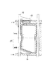
この配向分割型の液晶表示装置の構造について、図5,図6を参照しながら以下で更に詳しく説明する。図5は配向分割型液晶表示装置の一つの画素に注目した上面図であり、図6(a)は図5のA−A線断面図、同図(b)は図5のB−B線断面図である。
この液晶表示装置は、図6(a)や同図(b)に示すように、ガラス等からなる透明な下側基板6と上側基板7とが対向配置され、その間に液晶が封入されることで構成される。下側基板6の上にはゲートバスライン1A,1B、ドレインバスライン2、後述するリングCs5等が形成され、絶縁膜8を介してITO膜からなる画素電極4が形成されている。また、上側基板7上にはやはりITO膜からなる共通電極9が形成されており、これらの共通電極9,画素電極4間に電圧を印加することによってその間に封入された液晶分子10の方向を変えて駆動するものである。
【0005】
また、図には示していないが、液晶分子10に接する部分には液晶分子10の配向状態(特にプレチルト角)を規定するための配向膜が設けられている。図6(a)に示すように、下側基板6の側では第1の画素領域4Aのプレチルト角をαとし、第2の画素領域4Bのプレチルト角をβとしている(α>β)。逆に上側基板7の側では、第1の画素領域4Aのプレチルト角をβとし、第2の画素領域4Bのプレチルト角をαとすることにより、上側基板側のプレチルト角と下側基板側のプレチルト角とが互いに大−小という組み合わせになるようにしているので、図6(a)に示すように液晶分子10の配向状態が第1,第2の画素領域4A,4Bでは互いに逆になる。このようにすることによって液晶の配向方向が一方向に偏るのを防ぎ、視野角を拡大することができるのである。
【0006】
また、この液晶表示装置は、開口率を向上させるために通常画素電極を横切るように形成されている補助容量用の電極を環状にして、各画素の画素電極の周縁に沿うように配置している(これを以下でリングCsと称する)。このリングCsは、図5に示すように選択された画素に接続されたゲートバスライン(図5ではこれをn番目のゲートバスライン1Aとしている)の次段の画素に接続されたゲートバスライン(図5ではこれをn+1番目のゲートバスライン1Bとしている)と接続している。n番目のゲートバスライン1Aに接続された画素が選択された場合には、このn番目のゲートバスライン1Aの電位はTFT3のON/OFF動作をさせるため変動するが、n+1番目のゲートバスライン1Bの電位はこの間一定になっているので、この瞬間はn+1番目のゲートバスライン1Bに接続されたリングCs5も一定電位になっており、補助容量として機能しうるのである。このように次段のゲートバスラインとリングCsとが接続するように構成することにより、画素の開口率を向上させることが可能になるというものである。
【0007】
【発明が解決しようとする課題】
しかしながら、上述のような配向分割型の液晶表示装置を製造する際に、上側基板側のプレチルト角と下側基板側のプレチルト角とが互いに大−小という組み合わせになるようにする場合は、上側基板と下側基板の貼り合せの際のずれを避けることが非常に困難である。
【0008】
このような場合には、図7(a)に示すように、同一の画素領域において上側基板のプレチルト角と下側基板のプレチルト角とが一致してしまい、プレチルト角が大−大,小−小という組み合わせが生じる。例えば図7(a)の第2の画素領域4Bにおいては、上側基板と下側基板とで大きなプレチルト角αが互いに対向している状態になる。
【0009】
このような場合では、TNモードの液晶分子が本来あるべきツイスト状態にあるのみならず、上下から大きなプレチルト角αで液晶分子が圧力を受けることによってスプレイ状態も加わった状態になるので、通常のツイスト状態の液晶分子に比してエネルギー状態が高くなり、液晶分子の配向状態が不安定になる。ひどい場合には液晶の旋回方向が通常と逆になってしまうという不良(以下でこれを逆ツイストドメイン不良と称する)が生じる。
【0010】
この現象は印加電圧が高いほど発生しやすい。
従来構造では、図5や図6,図7等に示すように、リングCs5は画素電極4の形成領域から若干はみ出すように配置されている。補助容量として用いられる面積を確保しつつ、なるべく画素電極5とオーバーラップする領域を減らして開口率向上を図る為である。
【0011】
リングCsはゲートバスラインに接続されているが、このゲートバスラインにはTFTのON/OFFを制御するため液晶の印加電圧よりも高い電圧が印加されている(液晶への印加電圧は2〜3V程度だが、ゲートバスラインには±12V程度の電圧が印加される)。
【0012】
このような場合、図7(b)に示すように、画素電極の形成領域からはみだしたリングCsと、それに対向する共通電極との間に、高電界Eが生じるので、この付近の領域にある液晶分子はこの高電界Eの影響を受け、本来の配向状態と異なるような状態になってしまう場合がままある。この異常は画素の中央部の液晶分子にも伝搬して行くので、画素全体の液晶分子の配向がこれにより異状をきたしてしまう。
【0013】
特にこの異常は、液晶分子の配向状態が画素内でも不安定な第1,第2の画素領域4A,4Bの境界領域(以下でこれを配向分割領域と称する)のリングCS近傍の液晶分子において顕著であった。
この不安定が画素領域の中央まで波及し、ひいては逆ツイストドメイン不良が生じ、ディスクリネーションが生じることにより、当該液晶表示装置の表示画面がざらついてしまうという問題が生じていた。
【0014】
【課題を解決するための手段】
本発明は上記課題に鑑みてなされたものであって、複数のゲートバスラインと、前記ゲートバスラインと直交するように配置された複数のドレインバスラインと、前記ゲートバスライン及び前記ドレインバスラインで囲まれた画素領域内に前記ゲートバスライン及び前記ドレインバスラインに重ならないように配置された画素電極と、前記ゲートバスライン及び前記ドレインバスラインの交差する領域近傍に配置され、前記ゲートバスライン、前記ドレインバスライン及び前記画素電極と接続する液晶駆動用の素子であるTFTと、前記画素電極の配置領域の周縁に沿うように配置され、前記画素電極よりも下層に形成され、前記ゲートバスラインと接続する補助容量電極とを主面に備えた第1の透明基板と、主面に共通電極を備えた第2の透明基板とを有し、前記第1の透明基板と前記第2の透明基板とが対向配置され、その間に液晶が封入され、かつ前記画素領域が複数の領域に分割されてその各々の領域で前記液晶の配向状態が異なる液晶表示装置において、前記補助容量電極は、少なくとも前記複数の領域の境界部においては、前記画素電極の配置領域よりはみ出さないよう内側に配置されてなることを特徴とする液晶表示装置により、上記課題を解決するものである。
【0015】
引き続いて本発明の作用効果について以下で説明する。
本発明に係る液晶表示装置によれば、補助容量電極は、少なくとも複数の領域の境界部においては、画素電極の配置領域よりはみ出さないよう内側に配置されてなるため、ゲートバスラインに接続するため高電圧が印加される補助容量電極が画素電極によって電気的にシールドされることになる。
【0016】
従って、図7(b)に示すように従来生じていた補助容量電極と対向する共通電極との間の高電界Eが生じなくなるので、特に液晶分子の配向状態が不安定な複数領域の境界部の付近にある液晶分子がこの高電界Eの影響を受け、本来あるべき配向方向からずれるという異常の発生を抑止することができる。
これにより、従来装置で生じていたディスクリネーションや、これが原因となっていた表示画像のざらつきを極力抑止することが可能になる。
【0017】
【発明の実施の形態】
以下で、本発明の実施形態に係る液晶表示装置について図面を参照しながら説明する。この液晶表示装置は、TN(Twisted Nematic )モードの液晶表示装置であって、配向分割型構造をとっているものである。また、図1に示すようにリングCsを有することで、開口率の改善を図っている点では従来と同様である。
【0018】
本実施形態に係る液晶表示装置について図1,図2を参照しながら以下で更に詳しく説明する。図1は配向分割型液晶表示装置の一画素について説明する上面図であり、図2(a)は図1のX−X線断面図、同図(b)は図1のY−Y線断面図である。
この液晶表示装置は、図2(a)や同図(b)に示すように、ガラス等からなる第1の透明基板16と第2の透明基板17とが対向配置され、その間に液晶が封入されることで構成される。第1の透明基板16の上にはゲートバスライン11A,11B、ドレインバスライン12、リングCs15等が形成され、絶縁膜18を介してITO膜からなる画素電極14が形成されている。また、第2の透明基板17上にはやはりITO膜からなる共通電極19が形成されており、これらの共通電極19,画素電極14間に電圧を印加することによってその間に封入された液晶分子20の方向を変えて駆動するものである。
【0019】
また、図には示していないが、液晶分子20に接する部分には液晶分子20の配向状態(特にプレチルト角)を規定するための配向膜が設けられている。図2(a)に示すように、第1の透明基板16の側では第1の画素領域14Aのプレチルト角をαとし、第2の画素領域14Bのプレチルト角をβとしている(α>β)。逆に第2の透明基板17の側では、第1の画素領域14Aのプレチルト角をβとし、第2の画素領域4Bのプレチルト角をαとすることにより、第1の透明基板側のプレチルト角と第2の透明基板側のプレチルト角とが互いに大−小という組み合わせになるようにすることで視野角の拡大を図っている。
【0020】
また、この液晶表示装置は、開口率を向上させるために通常画素電極を横切るように形成されている補助容量用の電極を環状にして、各画素の画素電極の周縁に沿うように配置している(これを以下でリングCsと称する)。このリングCs15は、図1に示すように選択された画素に接続されたn番目のゲートバスライン11Aの次段の画素に接続されたn+1番目のゲートバスライン11Bと接続している。なお、このリングCsは補助容量電極の一例である。
【0021】
本実施形態の液晶表示装置は、図1に示すように、配向分割領域を含む全部の領域において上述のリングCs15の形成領域が画素電極14の形成領域内に収まっており、従来のように画素電極の形成領域からリングCsがはみ出さないように配置されている。
このため、リングCs15が上層の画素電極14によって完全に電気的にシールドされることになるので、たとえゲートバスラインにTFT駆動のための高電圧が印加されても、図7(b)に示す従来のようにリングCsと共通電極との間に生じていた高電界Eが生じなくなる。
【0022】
これにより、この付近にある液晶分子がこの高電界Eの影響を受け、本来あるべき配向方向からずれるという異常の発生を抑止することができる。
従って、従来装置で生じていたディスクリネーションや、これが原因となっていた画像のざらつきを抑止することが可能になる。
また、本実施形態では全部の領域で画素電極を用いて完全にリングCsをシールドしているが、液晶分子の異常が生ずるのはほとんどが配向分割領域の近傍なので、図3に示すように配向分割領域の部分のリングCsだけが画素電極の形成領域からはみ出さないようにしてシールドしても、この領域における液晶分子の配向状態の異状を抑止することができ、図1の装置とほぼ同様の効果を奏する。
【0023】
【発明の効果】
以上説明したように、本発明によれば、環状の補助容量電極は、少なくとも複数の領域の境界部においては、画素電極の配置領域よりはみ出さないよう内側に配置されてなるため、液晶分子の配向状態が不安定な複数領域の境界部の付近にある液晶分子が本来あるべき配向方向からずれるという異常の発生を抑止することができる。
【0024】
これにより、従来装置で生じていたディスクリネーションや、これが原因となっていた表示画像のざらつきを極力抑止することが可能になる。
【図面の簡単な説明】
【図1】本発明の実施形態に係る液晶表示装置を説明する上面図である。
【図2】本発明の実施形態に係る液晶表示装置を説明する断面図である。
【図3】本発明の別の実施形態に係る液晶表示装置を説明する上面図である。
【図4】配向分割型液晶表示装置の構成を説明する図である。
【図5】従来例に係る液晶表示装置を説明する上面図である。
【図6】従来例に係る液晶表示装置を説明する断面図である。
【図7】従来例に係る液晶表示装置の問題点を説明する断面図である。
【符号の説明】
11A n番目のゲートバスライン
11B n+1番目のゲートバスライン
12 ドレインバスライン
13 TFT
14 画素電極
14A 第1の画素領域
14B 第2の画素領域
15 リングCs(補助容量電極)
16 第1の透明基板
17 第2の透明基板
18 絶縁膜
19 共通電極
20 液晶分子[0001]
BACKGROUND OF THE INVENTION
The present invention relates to a liquid crystal display device, and more particularly to an improvement of a so-called alignment-divided liquid crystal display device in which a plurality of alignment films having different alignment states are provided in one pixel region in order to expand a viewing angle.
[0002]
[Prior art]
Hereinafter, an alignment-divided liquid crystal display device according to a conventional example will be described with reference to the drawings. This alignment-divided liquid crystal display device is a TN (Twisted Nematic) mode liquid crystal display device. As shown in FIG. 4, a plurality of
[0003]
Each
[0004]
The structure of this alignment-divided liquid crystal display device will be described in more detail below with reference to FIGS. 5A and 5B are top views focusing on one pixel of the alignment-divided liquid crystal display device. FIG. 6A is a cross-sectional view taken along line AA in FIG. 5, and FIG. 5B is a line taken along line BB in FIG. It is sectional drawing.
In this liquid crystal display device, as shown in FIGS. 6A and 6B, a transparent
[0005]
Although not shown in the drawing, an alignment film for defining the alignment state (particularly, the pretilt angle) of the
[0006]
Further, in this liquid crystal display device, in order to improve the aperture ratio, an auxiliary capacitor electrode that is usually formed so as to cross the pixel electrode is formed in an annular shape and arranged along the periphery of the pixel electrode of each pixel. (This is referred to as ring Cs below). This ring Cs is a gate bus line connected to a pixel next to a gate bus line connected to the selected pixel as shown in FIG. 5 (in FIG. 5, this is the nth gate bus line 1A). (In FIG. 5, this is the (n + 1) th gate bus line 1B). When a pixel connected to the nth gate bus line 1A is selected, the potential of the nth gate bus line 1A fluctuates to turn on / off the
[0007]
[Problems to be solved by the invention]
However, when manufacturing an alignment-divided liquid crystal display device as described above, if the pretilt angle on the upper substrate side and the pretilt angle on the lower substrate side have a combination of large and small, It is very difficult to avoid misalignment between the substrate and the lower substrate.
[0008]
In such a case, as shown in FIG. 7A, the pretilt angle of the upper substrate and the pretilt angle of the lower substrate coincide with each other in the same pixel region, and the pretilt angle is large—large, small— The combination of small arises. For example, in the
[0009]
In such a case, the TN mode liquid crystal molecules are not only in the twisted state as expected, but also in a state in which the splay state is added due to the liquid crystal molecules receiving pressure at a large pretilt angle α from above and below. The energy state becomes higher than the twisted liquid crystal molecules, and the alignment state of the liquid crystal molecules becomes unstable. In a severe case, there is a defect that the direction of rotation of the liquid crystal is reversed from the normal direction (hereinafter referred to as a reverse twist domain defect).
[0010]
This phenomenon is more likely to occur as the applied voltage is higher.
In the conventional structure, as shown in FIGS. 5, 6, 7, etc., the ring Cs <b> 5 is disposed so as to slightly protrude from the formation region of the
[0011]
The ring Cs is connected to the gate bus line, and a voltage higher than the applied voltage of the liquid crystal is applied to the gate bus line in order to control ON / OFF of the TFT (the applied voltage to the liquid crystal is 2 to 2). The voltage is about 3V, but a voltage of about ± 12V is applied to the gate bus line).
[0012]
In such a case, as shown in FIG. 7B, a high electric field E is generated between the ring Cs protruding from the pixel electrode formation region and the common electrode facing the ring Cs. The liquid crystal molecules are sometimes affected by the high electric field E and become different from the original alignment state. Since this abnormality propagates to the liquid crystal molecules in the center of the pixel, the orientation of the liquid crystal molecules in the entire pixel is thereby changed.
[0013]
In particular, this abnormality occurs in the liquid crystal molecules in the vicinity of the ring CS of the boundary region (hereinafter referred to as the alignment division region) between the first and
This instability spreads to the center of the pixel area, and thus a reverse twist domain defect occurs and disclination occurs, resulting in a problem that the display screen of the liquid crystal display device becomes rough.
[0014]
[Means for Solving the Problems]
The present invention has been made in view of the above problems, and includes a plurality of gate bus lines, a plurality of drain bus lines arranged to be orthogonal to the gate bus lines, the gate bus lines, and the drain bus lines. the surrounded by pixel regions in the gate bus lines and said drain bus pixel electrodes arranged so as not to overlap the line is arranged near the intersecting region of the gate bus lines and said drain bus line, the gate The TFT, which is a liquid crystal driving element connected to the bus line, the drain bus line, and the pixel electrode, is arranged along the periphery of the arrangement area of the pixel electrode, and is formed below the pixel electrode, A first transparent substrate having an auxiliary capacitance electrode connected to the gate bus line on the main surface, and a second transparent substrate having a common electrode on the main surface A bright substrate, the first transparent substrate and the second transparent substrate are arranged to face each other, a liquid crystal is sealed between them, and the pixel region is divided into a plurality of regions, In the liquid crystal display device in which the alignment state of the liquid crystal is different, the auxiliary capacitance electrode is arranged on the inner side so as not to protrude from the arrangement region of the pixel electrode at least at a boundary portion of the plurality of regions. The above-described problems are solved by the liquid crystal display device.
[0015]
Subsequently, the effects of the present invention will be described below.
According to the liquid crystal display device according to the present invention , the auxiliary capacitance electrode is arranged at least at the boundary portion of the plurality of regions so as not to protrude from the pixel electrode arrangement region, and is thus connected to the gate bus line. Therefore, the auxiliary capacitance electrode to which a high voltage is applied is electrically shielded by the pixel electrode.
[0016]
Therefore, as shown in FIG. 7B, the high electric field E between the auxiliary capacitance electrode and the common electrode facing the conventional electrode is not generated as shown in FIG. 7B. It is possible to suppress the occurrence of an anomaly that liquid crystal molecules in the vicinity of are affected by the high electric field E and deviate from the intended orientation direction.
As a result, it is possible to suppress as much as possible the disclination that has occurred in the conventional apparatus and the roughness of the display image caused by this.
[0017]
DETAILED DESCRIPTION OF THE INVENTION
Hereinafter, a liquid crystal display device according to an embodiment of the present invention will be described with reference to the drawings. This liquid crystal display device is a TN (Twisted Nematic) mode liquid crystal display device and has an alignment division type structure. Moreover, as shown in FIG. 1, it is the same as that of the prior art in that the aperture ratio is improved by having the ring Cs.
[0018]
The liquid crystal display device according to this embodiment will be described in more detail below with reference to FIGS. 1A and 1B are top views illustrating one pixel of an alignment-divided liquid crystal display device. FIG. 2A is a cross-sectional view taken along line XX in FIG. 1, and FIG. 1B is a cross-sectional view taken along line Y-Y in FIG. FIG.
In this liquid crystal display device, as shown in FIG. 2A and FIG. 2B, a first
[0019]
Although not shown in the drawing, an alignment film for defining the alignment state (particularly, the pretilt angle) of the
[0020]
Further, in this liquid crystal display device, in order to improve the aperture ratio, an auxiliary capacitor electrode that is usually formed so as to cross the pixel electrode is formed in an annular shape and arranged along the periphery of the pixel electrode of each pixel. (This is referred to as ring Cs below). The ring Cs15 is connected to the (n + 1) th gate bus line 11B connected to the pixel next to the nth gate bus line 11A connected to the selected pixel as shown in FIG. The ring Cs is an example of an auxiliary capacitance electrode.
[0021]
As shown in FIG. 1, the liquid crystal display device according to the present embodiment has the above-described ring Cs15 formation region within the
For this reason, since the ring Cs15 is completely electrically shielded by the
[0022]
As a result, it is possible to suppress the occurrence of an abnormality in which liquid crystal molecules in the vicinity are affected by the high electric field E and deviate from the orientation direction that should be originally formed.
Accordingly, it is possible to suppress disclination that has occurred in the conventional apparatus and image roughness caused by this.
Further, in this embodiment, the ring Cs is completely shielded by using the pixel electrode in the entire region, but the liquid crystal molecule abnormality is mostly generated in the vicinity of the alignment division region, so that the alignment is performed as shown in FIG. Even if only the ring Cs in the part of the divided region is shielded so as not to protrude from the pixel electrode formation region, the abnormal alignment state of the liquid crystal molecules in this region can be suppressed. The effect of.
[0023]
【The invention's effect】
As described above, according to the present invention, the annular auxiliary capacitance electrode is arranged on the inner side so as not to protrude from the arrangement area of the pixel electrode at least at the boundary between the plural areas. It is possible to suppress the occurrence of an abnormality in which the liquid crystal molecules in the vicinity of the boundary between the plurality of regions where the alignment state is unstable deviate from the alignment direction that should be originally formed.
[0024]
As a result, it is possible to suppress as much as possible the disclination that has occurred in the conventional apparatus and the roughness of the display image caused by this.
[Brief description of the drawings]
FIG. 1 is a top view illustrating a liquid crystal display device according to an embodiment of the present invention.
FIG. 2 is a cross-sectional view illustrating a liquid crystal display device according to an embodiment of the present invention.
FIG. 3 is a top view illustrating a liquid crystal display device according to another embodiment of the present invention.
FIG. 4 is a diagram illustrating a configuration of an alignment-divided liquid crystal display device.
FIG. 5 is a top view illustrating a liquid crystal display device according to a conventional example.
FIG. 6 is a cross-sectional view illustrating a liquid crystal display device according to a conventional example.
FIG. 7 is a cross-sectional view illustrating a problem of a liquid crystal display device according to a conventional example.
[Explanation of symbols]
11A nth gate bus line 11B n + 1th
14
16 First
Claims (4)
主面に共通電極を備えた第2の透明基板とを有し、
前記第1の透明基板と前記第2の透明基板とが対向配置され、その間に液晶が封入され、かつ前記画素領域が複数の領域に分割されてその各々の領域で前記液晶の配向状態が異なる液晶表示装置において、
前記補助容量電極は、少なくとも前記複数の領域の境界部においては、前記画素電極の配置領域よりはみ出さないよう内側に配置されてなることを特徴とする液晶表示装置。A plurality of gate bus lines; a plurality of drain bus lines arranged orthogonal to the gate bus lines; and the gate bus lines and the drains within a pixel region surrounded by the gate bus lines and the drain bus lines. and pixel electrodes arranged so as not to overlap the bus lines are arranged in the region near the intersection of the gate bus lines and said drain bus line, the gate bus line, a liquid crystal to be connected to the drain bus line and the pixel electrode The main surface includes a TFT which is a driving element and an auxiliary capacitance electrode which is arranged along the periphery of the pixel electrode arrangement region, is formed below the pixel electrode, and is connected to the gate bus line. A first transparent substrate;
A second transparent substrate having a common electrode on the main surface,
The first transparent substrate and the second transparent substrate are disposed to face each other, liquid crystal is sealed therebetween, and the pixel region is divided into a plurality of regions, and the alignment state of the liquid crystal is different in each region. In liquid crystal display devices,
2. The liquid crystal display device according to claim 1, wherein the auxiliary capacitance electrode is arranged on the inner side so as not to protrude from the arrangement area of the pixel electrode at least at a boundary portion between the plurality of areas.
Priority Applications (1)
| Application Number | Priority Date | Filing Date | Title |
|---|---|---|---|
| JP6699297A JP3847403B2 (en) | 1997-03-19 | 1997-03-19 | Liquid crystal display |
Applications Claiming Priority (1)
| Application Number | Priority Date | Filing Date | Title |
|---|---|---|---|
| JP6699297A JP3847403B2 (en) | 1997-03-19 | 1997-03-19 | Liquid crystal display |
Publications (2)
| Publication Number | Publication Date |
|---|---|
| JPH10260408A JPH10260408A (en) | 1998-09-29 |
| JP3847403B2 true JP3847403B2 (en) | 2006-11-22 |
Family
ID=13332021
Family Applications (1)
| Application Number | Title | Priority Date | Filing Date |
|---|---|---|---|
| JP6699297A Expired - Fee Related JP3847403B2 (en) | 1997-03-19 | 1997-03-19 | Liquid crystal display |
Country Status (1)
| Country | Link |
|---|---|
| JP (1) | JP3847403B2 (en) |
Families Citing this family (6)
| Publication number | Priority date | Publication date | Assignee | Title |
|---|---|---|---|---|
| US7561240B2 (en) | 1998-10-30 | 2009-07-14 | Samsung Electronics Co., Ltd. | Common electrode on substrate having non-depressed surface portion overlapping opening in pixel electrode on opposite substrate and depressed portion partially overlapping edge of the pixel electrode |
| KR100623984B1 (en) * | 1999-12-02 | 2006-09-13 | 삼성전자주식회사 | Liquid crystal displays having wide viewing angle and panels for the same |
| JP4162313B2 (en) * | 1998-12-28 | 2008-10-08 | シャープ株式会社 | Liquid crystal display |
| KR100635940B1 (en) * | 1999-10-29 | 2006-10-18 | 삼성전자주식회사 | A vertically aligned mode liquid crystal display |
| KR100740932B1 (en) * | 2001-04-20 | 2007-07-19 | 삼성전자주식회사 | Thin film transistor plate, fabricating method of the plate and liquid crystal display |
| CN109683411A (en) * | 2019-01-15 | 2019-04-26 | 深圳市华星光电技术有限公司 | A kind of dot structure and its display panel |
-
1997
- 1997-03-19 JP JP6699297A patent/JP3847403B2/en not_active Expired - Fee Related
Also Published As
| Publication number | Publication date |
|---|---|
| JPH10260408A (en) | 1998-09-29 |
Similar Documents
| Publication | Publication Date | Title |
|---|---|---|
| US6603524B1 (en) | LCD device having pixel electrodes asymmetrically overlapping gate and/or source signal lines | |
| JP2975844B2 (en) | Liquid crystal display | |
| US6950165B2 (en) | In-plane switching mode liquid crystal display device | |
| JP3234357B2 (en) | Liquid crystal display | |
| JP4381782B2 (en) | Liquid crystal display | |
| JP2859093B2 (en) | Liquid crystal display | |
| KR100921137B1 (en) | Liquid crystal display | |
| KR20020012367A (en) | liquid crystal display with wide viewing angle | |
| JPH06273803A (en) | Active matrix liquid crystal display device | |
| JP4658622B2 (en) | Substrate for liquid crystal display device and liquid crystal display device | |
| JP3383205B2 (en) | LCD panel | |
| JPH09152628A (en) | Active matrix substrate and display device having the same | |
| JPH09230387A (en) | Matrix type liquid crystal display device | |
| KR100327928B1 (en) | Liquid crystal display device | |
| JPH06294971A (en) | Liquid-crystal display device | |
| JP4087306B2 (en) | Liquid crystal display | |
| JP3847403B2 (en) | Liquid crystal display | |
| JPH10274783A (en) | Liquid crystal display device | |
| JPH10213816A (en) | Active matrix type liquid crystal display device | |
| JPH04305625A (en) | Liquid crystal display device | |
| JP2858499B2 (en) | Driving method of liquid crystal element | |
| JP2004046123A (en) | Liquid crystal display device | |
| JP2009134228A (en) | Liquid crystal display | |
| JP4121357B2 (en) | Liquid crystal display | |
| KR100827461B1 (en) | Cross field switchhing mode liquid crystla display |
Legal Events
| Date | Code | Title | Description |
|---|---|---|---|
| RD02 | Notification of acceptance of power of attorney |
Free format text: JAPANESE INTERMEDIATE CODE: A7422 Effective date: 20040302 |
|
| A521 | Written amendment |
Free format text: JAPANESE INTERMEDIATE CODE: A523 Effective date: 20040303 |
|
| A621 | Written request for application examination |
Free format text: JAPANESE INTERMEDIATE CODE: A621 Effective date: 20040303 |
|
| A711 | Notification of change in applicant |
Free format text: JAPANESE INTERMEDIATE CODE: A711 Effective date: 20050712 |
|
| A711 | Notification of change in applicant |
Free format text: JAPANESE INTERMEDIATE CODE: A711 Effective date: 20050713 |
|
| A521 | Written amendment |
Free format text: JAPANESE INTERMEDIATE CODE: A523 Effective date: 20050721 |
|
| RD02 | Notification of acceptance of power of attorney |
Free format text: JAPANESE INTERMEDIATE CODE: A7422 Effective date: 20050721 |
|
| A521 | Written amendment |
Free format text: JAPANESE INTERMEDIATE CODE: A523 Effective date: 20050818 |
|
| A977 | Report on retrieval |
Free format text: JAPANESE INTERMEDIATE CODE: A971007 Effective date: 20060413 |
|
| A131 | Notification of reasons for refusal |
Free format text: JAPANESE INTERMEDIATE CODE: A131 Effective date: 20060516 |
|
| A521 | Written amendment |
Free format text: JAPANESE INTERMEDIATE CODE: A523 Effective date: 20060705 |
|
| TRDD | Decision of grant or rejection written | ||
| A01 | Written decision to grant a patent or to grant a registration (utility model) |
Free format text: JAPANESE INTERMEDIATE CODE: A01 Effective date: 20060822 |
|
| A61 | First payment of annual fees (during grant procedure) |
Free format text: JAPANESE INTERMEDIATE CODE: A61 Effective date: 20060823 |
|
| R150 | Certificate of patent (=grant) or registration of utility model |
Free format text: JAPANESE INTERMEDIATE CODE: R150 |
|
| FPAY | Renewal fee payment (prs date is renewal date of database) |
Free format text: PAYMENT UNTIL: 20090901 Year of fee payment: 3 |
|
| FPAY | Renewal fee payment (prs date is renewal date of database) |
Free format text: PAYMENT UNTIL: 20100901 Year of fee payment: 4 |
|
| FPAY | Renewal fee payment (prs date is renewal date of database) |
Free format text: PAYMENT UNTIL: 20110901 Year of fee payment: 5 |
|
| FPAY | Renewal fee payment (prs date is renewal date of database) |
Free format text: PAYMENT UNTIL: 20120901 Year of fee payment: 6 |
|
| FPAY | Renewal fee payment (prs date is renewal date of database) |
Free format text: PAYMENT UNTIL: 20130901 Year of fee payment: 7 |
|
| LAPS | Cancellation because of no payment of annual fees |