JP3841190B2 - Liquid crystal element manufacturing method and manufacturing apparatus thereof - Google Patents
Liquid crystal element manufacturing method and manufacturing apparatus thereof Download PDFInfo
- Publication number
- JP3841190B2 JP3841190B2 JP22936097A JP22936097A JP3841190B2 JP 3841190 B2 JP3841190 B2 JP 3841190B2 JP 22936097 A JP22936097 A JP 22936097A JP 22936097 A JP22936097 A JP 22936097A JP 3841190 B2 JP3841190 B2 JP 3841190B2
- Authority
- JP
- Japan
- Prior art keywords
- liquid crystal
- substrates
- pair
- region
- manufacturing
- Prior art date
- Legal status (The legal status is an assumption and is not a legal conclusion. Google has not performed a legal analysis and makes no representation as to the accuracy of the status listed.)
- Expired - Fee Related
Links
Images


Landscapes
- Liquid Crystal (AREA)
Description
【0001】
【発明の属する技術分野】
本発明は、液晶パネル等の液晶素子の製造方法、並びにその製造装置に関する。
【0002】
【従来の技術とその問題点】
液晶パネル等の液晶素子の製造方法として、従来、良く知られているものに注入法が有る。この注入法では、まず、1〜10μmの所定間隔を置いて対向配置した一対の基体の周辺部分をシール材によって接着固定して空のパネルを作製する。次に、この空のパネルを真空装置内に収容して、パネル内部を真空状態とし、シール材部に予め設けた注入口を液晶に浸す。その後、真空装置内を徐々に大気圧に戻すことにより、パネル内外の圧力差と毛細管現象を利用して液晶をパネル内に注入する。しかしながら、この注入法では、粘性の比較的高い液晶の注入に時間がかかり、特に、液晶表示素子の大型化に伴い多大な注入時間を要するようになるという問題が有った。また、真空装置内を真空とするための前処理時間がかかるという問題も有り、更に、高価な真空装置が必要であるという問題も有った。即ち、従来の注入法では、製造時間の増大やコストの上昇といった問題が有った。
【0003】
そこで、例えば、特開昭60−75817号、特開昭60−230636号、特開平1−303414号、特開平3−25416号、特開平4−218027号の各公報に記載されているように、一対の基体の一方に表示領域を囲むようにシール材を塗布し、その表示領域に液晶を滴下又は塗布した後、真空装置内で、もう一方の基体を平行に圧着し、その後、シール材を硬化させる方法(滴下法又は塗布法)が提案されている。この方法によれば、液晶注入に要する時間は大幅に短縮されるが、真空下で基体の重ね合わせを行うため、やはり、真空装置内を真空にするための前処理時間がかかり、また、高価な真空装置が必要なため、製造時間が増大し、製造コストが嵩むという問題が有った。
【0004】
また、特開平2−84616号、特開平2−123324号、特開平6−208097号の各公報に記載されているように、上述した滴下法又は塗布法において、基体の重ね合わせを大気中で行う方法も提案されている。この方法では真空装置が不要のため、上述した真空装置を用いる滴下法又は塗布法と比較して、製造時間及び製造コストを抑えることができる。しかしながら、この方法では、大気中で基体を重ね合わせるため、その重ね合わせの際に表示領域内の液晶中に気泡が残留してしまい、これが表示欠陥になって、歩留りが低下するという問題が有った。
【0005】
また、上述のような気泡の残留の問題を解決するために、液晶を細線状の所定パターンに塗布し、基体を徐々に又は間欠的に重ね合わせる方法(特開平3−89315号公報)や、一対の基板を楔型をなすように対向させ、或いは、一方の基板を凸状に反らせた状態で対向させ、徐々に基板同士が平行となるように接近させて圧着させる方法(特開平4−179919号公報)等が提案されている。しかしながら、このような方法では、基体の重ね合わせに要する時間が長くなり、また、精密な基体の重ね合わせを行うために特殊な装置が必要となって、やはり、製造時間の増大や製造コストが嵩むという問題が有った。
【0006】
そこで、本発明の目的は、特に真空装置を必要とせず、大気中で且つ液晶中に気泡が残留することなく短時間で且つ簡便に液晶の封入を行うことのできる液晶素子の製造方法並びにその製造装置を提供することである。
【0007】
【課題を解決するための手段】
上述した目的を達成する本発明の液晶素子の製造方法は、所定間隔を置いて対向配置された一対の基体がその外周部に沿って設けられた接着領域において互いに固着され、前記一対の基体間の前記接着領域の内側の液晶領域に液晶が封入された液晶素子の製造方法であって、前記一対の基体の少なくとも一方の基体の前記接着領域に硬化性接着剤を塗布する工程と、前記一対の基体の少なくとも一方の基体の前記液晶領域の一端部に所定量の液晶を供給する工程と、前記硬化性接着剤及び前記液晶を間に挟んで前記一対の基体を対向配置する工程と、対向配置された前記一対の基体を同一温度に加熱する工程と、対向配置された前記一対の基体の少なくとも一方の基体の上を前記液晶領域の前記一端部から他端部の方向へヒーター内蔵の加圧ローラーを相対的に転動させ、この際、前記加圧ローラーを内蔵ヒーターによって前記基体と同一の温度に加熱して、前記液晶を前記一端部から前記液晶領域の全体へ展延させる工程と、前記硬化性接着剤を硬化させる工程とを有する。
【0008】
本発明の一態様では、前記液晶領域が表示領域であり、対向配置された前記一対の基体の少なくとも一方の基体の上を前記液晶領域の前記一端部から他端部の方向へ前記加圧ローラーを転動させて、前記液晶を前記一端部から前記液晶領域の全体へ展延させる。
【0009】
本発明の一態様では、前記加圧ローラーを、対向配置された前記一対の基体の少なくとも一方の基体の上を相対的に転動させる際、前記液晶領域の前記一端部よりも外側の前記一方の基体の端縁部寄りの位置から前記液晶領域の前記他端部まで相対的に転動させる。
【0010】
本発明の一態様では、相対的に移動する前記基体をその移動方向に前記加圧ローラーで加圧し、更にこの加圧状態を補助ローラーで保持する。
【0011】
本発明の一態様では、前記加圧ローラーを大径に形成し、前記補助ローラーを前記加圧ローラーより小径に形成する。
【0012】
本発明の一態様では、前記接着領域に前記硬化性接着剤を塗布する際、前記液晶領域の前記他端部の近傍に前記硬化性接着剤を塗布しない空気排出部を少なくとも1か所設ける。
【0013】
本発明の一態様では、前記一対の基体の少なくとも一方の基体の対向面における前記液晶領域と前記接着領域との間に溝を設け、前記液晶を展延させる際、少なくとも余剰の前記液晶を前記溝内に収容させる。
【0014】
本発明の一態様では、前記一対の基体を対向させた時に前記液晶領域を平面的に見て閉ループ状に取り囲むように前記溝を連続させる。
【0015】
本発明の一態様では、前記一対の基体の少なくとも一方の基体の前記対向面に形成した前記溝に連続して前記一方の基体の端縁にまで延びる空気排出溝を設け、前記液晶を展延させる際、前記液晶により押し出された空気を前記空気排出溝から排出させる。
【0016】
本発明の一態様では、前記溝として、幅200μm以上、深さ20μm以上の溝を形成する。
【0017】
本発明の一態様では、前記液晶として、強誘電性液晶を用いる。
【0018】
本発明の一態様では、前記液晶中に、平均一次粒径が1μm以下の微粒子を混入する。
【0019】
本発明の一態様では、前記液晶を展延させる際、その液晶材料のスメクチックA相とコレステリック相との間の転移温度とそれよりも4℃高い温度との間で且つコレステリック相と等方相との間の転移温度以下に前記基体を加熱する。
【0020】
本発明の一態様では、前記液晶を展延させる工程の後、対向配置されている前記一対の基体をその両面から均一に加圧しながら、又は、加圧した後、前記硬化性接着剤を硬化させる。
【0021】
また、本発明で得られる液晶素子では、所定間隔を置いて対向配置された一対の基体がその外周部に沿って設けられた接着領域において互いに固着され、前記一対の基体間の前記接着領域の内側の液晶領域に液晶が封入され、前記一対の基体の少なくとも一方の基体の対向面における前記液晶領域と前記接着領域との間に溝が設けられているのがよい。
【0022】
その一態様では、前記液晶領域が表示領域である。
【0023】
その一態様では、前記一対の基体を対向させた時に前記液晶領域を平面的に見て閉ループ状に取り囲むように前記溝が連続する。
【0024】
その一態様では、前記一対の基体の少なくとも一方の基体の前記対向面に形成された前記溝に連続して前記一方の基体の端縁にまで延びる溝が更に設けられている。
【0025】
その一態様では、前記溝の幅が200μm以上、深さが20μm以上である。
【0026】
その一態様では、前記液晶が強誘電性液晶である。
【0027】
その一態様では、前記液晶中に、平均一次粒径が1μm以下の微粒子が混入されている。
【0028】
本発明の液晶素子の製造装置では、所定の間隔を置いて対向配置された一対の基体がその外周部に沿って設けられた接着領域において互いに固着され、前記一対の基体間の前記接着領域の内側の液晶領域に液晶が封入された液晶素子の製造装置であって、前記一対の基体の少なくとも一方の基体の前記接着領域に硬化性接着剤を塗布する塗布手段と、前記一対の基体少なくとも一方の基体の前記液晶領域の一端部に所定量の液晶を供給する供給手段と、前記硬化性接着剤及び前記液晶を間に挟んで前記一対の基体を対向配置する配置手段と、対向配置された前記一対の基体を同一温度に加熱する加熱手段と、対向配置された前記一対の基体の少なくとも一方の基体の上を前記液晶領域の前記一端部から他端部の方向へ相対的に転動し、この際、内蔵ヒーターによって前記基体と同一の温度に加熱されて、前記液晶を前記一端部から前記液晶領域の全体へ展延させるヒーター内蔵の加圧ローラーと、前記硬化性接着剤を硬化させる硬化手段とを有する。
【0029】
本発明の一態様では、前記液晶領域が表示領域であり、対向配置された前記一対の基体の少なくとも一方の基体の上を前記液晶領域の前記一端部から他端部の方向へ前記加圧ローラーが転動することにより、前記液晶が前記一端部から前記液晶領域の全体へ展延される。
【0030】
本発明の一態様では、前記加圧ローラーが、対向配置された前記一対の基体の少なくとも一方の基体の上を相対的に転動する際、前記液晶領域の前記一端部よりも外側の前記一方の基体の端縁部寄りの位置から前記液晶領域の前記他端部まで相対的に転動する。
【0031】
【発明の実施の形態】
以下、本発明を好ましい実施の形態に従い説明する。
【0032】
まず、図1〜図3を参照して、アクティブマトリクス方式の液晶パネル等の液晶表示素子の製造方法の例を説明する。
【0033】
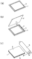
まず、図1(a)及び(b)に示すように、アクティブマトリクス方式の液晶表示素子を構成する上下一対の基体1、2を用意する。例えば、基体1は、ガラス基体上にマトリクス状の画素電極(図5(a)参照)とそれらの画素電極に接続された薄膜トランジスタ(不図示)を有し、更に、その上に配向膜(不図示)を有している。一方、基体2は、ガラス基体上にカラーフィルター(不図示)と透明共通電極(図5(a)参照)と配向膜(不図示)とを有している。
【0034】
そこで、まず、図1(a)に示すように、例えば、基体1の配向膜が形成された対向面においてその外周部に沿った接着領域に、例えば、紫外線硬化型接着剤からなるシール材3をディスペンサを用いて、図示の如く、接着領域の内側の表示領域を閉ループ状に囲むように塗布する。なお、シール材3は、基体2の配向膜が形成された対向面の側に塗布しても良く、また、両方の基体の対向面に塗布しても良い。
【0035】
次に、図1(b)に示すように、基体1の対向面における表示領域の一端部に、液晶4を、例えば、ディスペンサを用いて正確に計量して、基体1の一辺に沿って直線状に滴下する。なお、液晶4は、基体2の対向面の側に塗布しても良く、また、両方の基体の対向面に塗布しても良い。更に、液晶4の塗布パターンは、直線状に限らず、曲線状や点線状でも良い。更に、液晶4の広がりの均一性を増す目的で、表示領域内の他の箇所にも滴下して良い。
【0036】
なお、この例で用いる液晶4は、例えば、常温で流動性を持ったネマティックタイプのもので、そのままで動作可能なものとする。また、液晶4は、基体間ギャップを制御するためのスペーサ粒子を混合して用いるのが好ましい。なお、スペーサ粒子は、予め一方又は両方の基体の対向面に散布しておいても良く、更に、その場合、基体を加熱して、熱可塑性樹脂をコーティングしたスペーサ粒子を基体に固着させておいても良い。
【0037】
次に、図1(c)に示すように、基体1と2を、夫々の対向面が向かい合うようにして重ね合わせ、例えば、上から重ね合わせた基体2の自重によって液晶4が広がり、近接した接着領域の近傍の表示領域内に行き渡るのを待つ。この後、例えば、基体2の上を加圧ローラー5を転動させ、図3(a)に示すように、液晶4を表示領域の全体に展延させる。また、液晶4に混合したスペーサ粒子も液晶4とともに表示領域の全体に分布し、基体1、2間に所定のギャップが形成される。このように、加圧ローラー5によって液晶4を一方向に展延させることにより、一旦液晶4に巻き込まれた気泡が液晶4の展延に伴って液晶4内から押し出される。また、液晶4が横に広がってシール材3のシール部に侵入しない。
【0038】
この時の加圧ローラー5の押圧力は2〜15kg/cm2の範囲であるのが好ましい。これよりも押圧力が小さいと、液晶4が充分に展延せず、また、所定の基体間ギャップが得られない虞が有る。また、逆にこの範囲よりも押圧力が大きいと、基体の対向面に設けられた配向膜が損傷したり、基体間ギャップ保持のためのスペーサ粒子が破壊してしまってやはり所定の基体間ギャップが得られなくなる虞が有る。
【0039】
また、図3(b)に模式的な断面図を示すが、加圧ローラー5は、一点鎖線で示すように、最初に液晶4を塗布した位置よりも外側の基体2の端縁寄りの位置から転動を開始させるのが良い。これにより、液晶4は、最初に塗布した表示領域の一端部から他端部に向かって確実に押し広げられて行く。また、この時、シール材3は未だ充分に基体2に密着していないので、所々に隙間100が形成されており、これらの隙間100から適度に空気が抜けて、液晶4に気泡が残留するのが防止されるとともに、シール材3のシールパターンの乱れや破れが防止される。更に、例えば、基体1、2上の透明電極101上に形成された例えばポリイミドのラビング膜からなる配向膜102の図示したラビング方向に加圧ローラー5を転動させると、液晶4の分子103がその方向に配向し易くなる。
【0040】
なお、加圧手段としては、図示した加圧ローラー5に限らず、また、加圧ローラーを相対的に移動させる際、基体1、2の側を移動させても良い。
【0041】
次に、図2に示すように、液晶4が充填された表示領域をステンレス板6等で遮蔽し、紫外線ランプ7により紫外線を照射してシール材3を硬化させる。なお、このシール材3の硬化に先立って、又は、硬化させる際に、対向配置された基体1、2の上下両面から加熱プレス等により均一に加圧するのが好ましい。これにより、均一な基体間ギャップが得られ、表示むらの無い高品位の液晶表示素子を得ることができる。
【0042】
この例では、一対の基体1、2のうちの少なくとも一方の基体1の上の、シール材3が塗布された接着領域の内側の表示領域の一端部に液晶4を供給し、基体1、2を対向配置して重ね合わせた後、液晶4を供給した表示領域の一端部から他端部の方向に加圧ローラー5を転動させて、液晶4をその一端部から他端部の方に押し広げ、表示領域の全体に行き渡らせる。従って、液晶4の充填を短時間で行うことができる。また、この液晶4の展延を大気圧下で行っても、一旦液晶4に巻き込まれた気泡が液晶4の展延に伴って液晶4内から押し出されるので、液晶4内に気泡が残留することが無い。従って、従来のように高価な真空装置を用いる必要が無いため、製造コストが嵩むことが無い。更に、基体1、2を重ね合わせる際に、基体1又は2を無理な姿勢に保持する必要が無いので、基体1、2の正確な重ね合わせを簡便且つ短時間に行うことができる。更に、加圧ローラー5の押圧を適度に調整することで、所望の基体間ギャップを得ることができる効果も有る。
【0043】
次に、図4を参照して、別の例を説明する。なお、この例において、上述した第1の例に対応する部位には上述した第1の例と同一の符号を付す。
【0044】
図4(a)に示すように、この第2の例では、基体1の接着領域にシール材3を塗布する際、液晶4を滴下する側から遠い側の辺に、シール材3を塗布しない空気排出部8を設ける。これにより、図4(b)に示すように、加圧ローラー5を転動させた時、展延する液晶4によって押し出される空気が空気排出部8から円滑に排出される。なお、空気排出部8は1か所に限らず複数箇所に設けても良い。また、その場合、液晶4を滴下する側から遠い側の辺以外の辺にも空気排出部を設けて良い。
【0045】
空気排出部8は、図4(c)に示すように、シール材3を硬化させた後、封止材を塗布して封止する。
【0046】
上に説明した以外の構成は、既述した第1の例と同じである。
【0047】
この第2の例では、上述した第1の例の効果に加え、液晶4内に気泡が残留することをより効果的に防止できるとともに、シール材3のシールパターンの乱れや接着領域内端部での空気の残留が無い液晶表示素子を得ることができるという効果が得られる。
【0048】
図5〜図6に第3の例を示す。この第3の例において、上述した第1及び第2の例に対応する部位にはそれらの例と同一の符号を付す。
【0049】
図5(a)及び(b)に示すように、この第3の例では、配向膜を形成するに先立って、基体1、2の夫々の対向面の接着領域の内側の位置に溝9a、9bを設ける。これらの溝9a、9bは、各基体1、2に設けられる電極の引き出し部と干渉しないようなパターンに形成する。例えば、図示の例では、基体1に画素電極104が設けられるので、これらの画素電極104の引き出し部を避けて、表示領域の4隅に溝9aを設ける。一方、基体2には透明共通電極105が設けられるので、表示領域の4辺に比較的長い溝9bを形成することができる。そして、これらの溝9a、9bは、図6(b)に示すように、基体1と2を対向配置した時に互いに重なり合って、表示領域を閉ループ状に取り囲むように連続する。
【0050】
このような溝9a、9bを設けると、図6(a)に示すように、加圧ローラー5によって液晶4を展延させた際、図6(b)に示すように、余剰の液晶が有ってこれらが本来の表示領域からはみ出す場合には、その余剰の液晶が溝9a、9bに収容される。従って、その余剰の液晶がシール材3のシール部に侵入することが無く、液晶がシール材に接触することによる表示品位の低下やパネルの接着不良を来すことが無い。また、液晶4の滴下量の精度を必要としないため、工程が簡便になる。また、これらの溝9a、9bは、接着領域からはみ出してきたシール材3を収容する場合にも役立つ。
【0051】
なお、この液晶やシール材を収容する効果は、図6(b)に示すように、溝9a、9bを連続させた場合に特に大きいが、溝9a、9bは必ずしも連続させなくとも良い。
【0052】
また、形成する溝の幅は200μm以上とし、深さは20μm以上とするのが好ましい。これより幅の狭い又は深さの浅い溝では、余剰の液晶やシール材が表示領域や接着領域からはみ出してきた時にそれらを充分に収容することができず、従って、溝を設けた効果が充分に得られず、高品位の液晶表示素子を得られなくなる虞が有る。また、溝の深さの上限は、基体の機械的強度を低下させないという観点から、基体の厚さの半分以下であるのが好ましい。
【0053】
この第3の例において、上に説明した以外の構成は、既述した第1の例と同じである。
【0054】
図7に第4の例を示す。この第4の例において、上述した第1〜第3の例に対応する部位にはそれらの例と同一の符号を付す。
【0055】
図7に示すように、この第4の例は、上述した第2の例と同様に基体1の接着領域にシール材3を塗布しない空気排出部8を設けた以外は、上述した第3の例と同じ構成である。従ってこの第4の例では、上述した第2及び第3の例の効果を夫々得ることができる。
【0056】
図8に第5の例を示す。この第5の例において、上述した第1〜第4の例に対応する部位にはそれらの例と同一の符号を付す。
【0057】
図8に示すように、この第5の例では、上述した第3の例と同様の構成において、表示領域の液晶4を供給する辺とは反対側の辺に対応して基体2に設けた溝9bに連続して、その基体2の端縁まで延びる溝9cを設けている。これ以外の構成は、上述した第3の例と同じである。
【0058】
この第5の例において設けた溝9cは、加圧ローラー5によって液晶4を展延させた時に、液晶4によって押し出された空気を排出する空気排出溝として機能する。従って、この第5の例では、空気排出部8を設けた第2及び第4の例と同様に、液晶4内に気泡が残留することを効果的に防止できるとともに、シール材3のシールパターンの乱れや接着領域内端部での空気の残留が無い液晶表示素子を得ることができるという効果が得られる。更に、この第5の例の溝9cは、それが連続した溝9bを補助する作用が有るので、例えば、その溝9bに収容しきれない液晶やシール材を溝9cに収容できるという効果も有る。
【0059】
この溝9cは、既述した第2及び第4の例における空気排出部8と同様、シール材3を硬化させた後、封止材により封止する。
【0060】
なお、溝9cは、1本に限らず、複数本設けても良く、また、その場合、他の辺の溝9bに連続して設けても良い。また、溝9cは、基体1の側に設けても良い。更に、溝9cは曲線状に設けても良い。
【0061】
図9に本発明に基づく例を示す。この例において、上述した第1〜第5の例に対応する部位にはそれらの例と同一の符号を付す。
【0062】
この例では、強誘電性液晶を用いた単純マトリクス方式の液晶パネル等の液晶表示素子の製造工程に本発明を適用した例を示す。
【0063】
まず、図9(a)に示すように、単純マトリクス方式の液晶表示素子を構成する上下一対の基体11、12を用意する。例えば、基体11は、ガラス基体上にストライプ状の透明電極(図10(a)参照)を有し、更に、その上に配向膜(不図示)を有している。一方、基体12は、ガラス基体上にカラーフィルター(不図示)とストライプ状の透明電極(図10(a)参照)と配向膜(不図示)とを有している。これらの基体11、12を、ストライプ状の透明電極が互いに直交するように重ね合わせることにより、単純マトリクスが形成される。
【0064】
そして、図9(a)に示すように、上述した第2の例の場合と同様にシール材3に空気排出部8を設けた基体11の表示領域の一端部に強誘電性液晶14を滴下する。この時、図示の如く、基体11をヒーター内蔵ステージ20の上に載置して、基体11を、強誘電性液晶14のスメクチックA相とコレステリック相との間の転移温度とそれより4℃高い温度との間で且つコレステリック相と等方相との間の転移温度以下の温度に加熱しながら、例えば、保温ディスペンサを用いて正確に計量して強誘電性液晶14の滴下を行うのがよい。
【0065】
また、この際、その強誘電性液晶14中に、スペーサ粒子とともに、平均一次粒径が1μm以下の微粒子を混入させるのが好ましい。本願出願人が特開平6−194693号公報において既に提示したように、液晶中にこのような微粒子を存在させると、例えば、この微粒子の誘電率により液晶の透過率が印加電圧に応じて連続的に変化することにより、強誘電性液晶表示素子において、高コントラストを保持しつつアナログ階調表示を実現することができる。使用可能な微粒子の具体例としては、酸化チタンやカーボンブラックを挙げることができる。
【0066】
このような微粒子を用いる場合、注入法のように長時間を要するプロセスでは、注入時に微粒子の凝集や沈降が起こる懸念が有るが、本例の場合にはその懸念は殆ど無い。
【0067】
次に、図9(b)に示すように、基体11と同じ温度に加熱した基体12を基体11に重ね合わせ、例えば、ランプヒーター21を内蔵したヒーター内蔵加圧ローラー15を転動させて、強誘電性液晶14を展延させる。
【0068】
強誘電性液晶は一般に粘度が高いため、低い温度で液晶を展延させると流動抵抗により配向膜を損傷してしまい、液晶の均一な配向状態が得られなくなる。しかし、基体を加熱し、液晶をコレステリック相又は等方相に保つと、液晶の粘度が充分に低下し、展延に際して配向膜を損傷させることが無い。しかしながら、等方相で展延したり、或いは、コレステリック相であってもスメクチックA相とコレステリック相との間の転移温度よりも4℃高い温度を越える温度で液晶を展延すると、基体間ギャップ制御のために用いるスペーサ粒子の周辺の配向が乱れ、反転ドメインが形成されてしまう。このため、表示品位が低下するという問題が生じる。そこで、液晶材料のスメクチックA相とコレステリック相との間の転移温度とそれより4℃高い温度との間で且つコレステリック相と等方相との間の転移温度以下の温度に加熱しながら強誘電性液晶の展延を行うことにより、液晶の配向乱れの無い高品位の液晶表示素子を得ることができる。
【0069】
しかる後、図9(c)に示すように、既述した第2の例と同様にして、シール材3を硬化させた後、空気排出部8を封止する。
【0070】
上に説明した以外の構成は、既述した第2の例と同じである。
【0071】
この例では強誘電性液晶を用いているが、強誘電性液晶はメモリ性を持つために、CRT(陰極線管)等で問題となっているフリッカーを無くすことができる。また、強誘電性液晶は、ネマチック液晶表示と比較して約1000倍も高速応答であるため、本例のような単純X−Yマトリクス駆動でも1000本以上の走査線で駆動できる(即ち、薄膜トランジスタ(TFT)での駆動を無くせる。)。更に、強誘電性液晶は視野角依存性が少ない。従って、この例により、安価で高品位の液晶表示素子を得ることができる。
【0072】
そして、この例により、粘度が高いために通常の注入法では液晶注入に多大な時間を要していた強誘電性液晶を極めて短時間で充填できるようになる。
【0073】
図10に本発明に基づく他の例を示す。この例において、上述した例に対応する部位にはその例と同一の符号を付す。
【0074】
この例では、上記した例と同様に強誘電性液晶を用いた単純マトリクス方式の液晶パネル等の液晶素子の製造工程に本発明を適用した他の例を示す。
【0075】
まず、図10(a)及び(b)に示すように、上記した例と同様に基体11、12を、ストライプ状の透明電極が互いに直交するように重ね合わせて単純マトリクスを形成し、同様の条件で、シール材3に空気排気部8を設けた基体11の表示領域の一端部に強誘電性液晶14を滴下する。
【0076】
次に、図10(c)に示すように、基体11と同じ温度に加熱した基体12を基体11に重ね合わせ、例えば、ランプヒーター21を内蔵したヒーター内蔵加圧ローラー15を転動させて、強誘電性液晶14を展延させる。そして、更に加圧ローラー15の下流側において、ランプヒーター23を内蔵した補助ローラー22A、22Bを転動させ、加圧ローラー15が通過後は補助ローラー22A、22Bで基体11及び12を保持させる。
【0077】
しかる後、図10(d)に示すように、既述した第2の例と同様にして、シール材3を硬化させた後、空気排出部8を封止する。
【0078】
上に説明した以外の構成は、既述した第2の例と同じである。
【0079】
なお、基体間ギャップを制御するスペーサ粒子を配する方法としては、液晶中に混合するのみならず、予め少なくとも一方の基体に散布しておいても良い。更に、この場合、熱可塑性樹脂をコートしたスペーサ(例えば、宇部日東化成株式会社製のハイプレシカ)を散布し、基体を加熱してこのスペーサ粒子を基体に固着させておいてもよい。
【0080】
また、強誘電性液晶にアナログ階調表示性を与える超微粒子の物性、種類等は種々に変更することができる。
【0081】
この例では、上述した例の効果に加え、この補助ローラー22A、22Bにより、加圧ローラー15の通過後の基体11、12が保持されると共に、加圧ローラー15に加圧された未硬化のシール材3の反発力に伴うギャップ戻り(ギャップの変動)を防ぐことができる。
【0082】
図13に本発明の更に別の例を示す。この例において、上述した各例に対応する部位にはそれらの例と同一の符号を付す。
【0083】
図13(a)に示すように、この例では、上述した図9の例の強誘電性液晶を用いた単純マトリクス方式の液晶表示素子において、既述した第4の例と同様に、基体11、12の対向面に夫々溝19a、19bを設ける。但し、この例では、図示の如く、基体11、12の対向面に夫々ストライプ電極106、107が設けられるので、溝19a、19bは、それらのストライプ電極106、107の引き出し部が無い2辺に沿って夫々設けられる。また、図13(b)に示すように、溝19a、19bは、基体11と12を対向配置した時に互いに重なり合って、表示領域を閉ループ状に取り囲むように連続するパターンに設けられる。
【0084】
この例において、上に説明した以外の構成は、上述した図9の例と同じである。
【0085】
この例では、上述した図9の例の効果に加え、既述した第4の例と同様の効果が得られる。
【0086】
以上の各例、特に図9、図10の例では、液晶パネル等の液晶表示素子及びその製造方法に本発明を適用した例を説明したが、本発明は、例えば、光を遮蔽するシャッターのような液晶素子及びその製造方法にも適用が可能である。また、例えば、強誘電性液晶を用いたアナログ階調表示による調光素子等の液晶素子及びその製造方法にも本発明は適用が可能である。
【0087】
【実施例】
例1
図1〜図3に示した第1の例に従い、アクティブマトリクス方式の液晶表示素子を作製した。
【0088】
まず、第1の例で説明したアクティブマトリクス方式の液晶表示素子を構成する上下一対の基体1、2を用意した。
【0089】
次に、図1(a)に示すように、基体1の外周部に沿って閉ループ状をなすようにディスペンサを用いてシール材3(協立化学産業(株)製 ワールドロック No.SD−11Z)を塗布し、60℃で3分間レベリングしてシール部を形成した。
【0090】
次に、図1(b)に示すように、基体1の一辺に沿って、上述したシール部の内側に、予め0.05wt%のスペーサ粒子を混合しておいた液晶4を、ディスペンサを用いて正確に計量して、直線状に滴下した。
【0091】
次いで、基体1と2を、夫々の配向膜形成面を向かい合わせるようにして重ね合わせた。上から重ね合わせた基体2の自重によって液晶4が広がり、液晶4がこれに近接したシール部との間の領域に行き渡るのを待ってから、図1(c)に示すように、液晶4を滴下した側のシール部の外側から直径90mmの加圧ローラー5を4kg/cm2の圧力で押圧転動させた。これにより、シール部の内側のほぼ全域にわたって液晶4が一様に展延し、且つ、液晶4に予め混合したスペーサ粒子も液晶4とともにシール部の内側全域に行き渡り、基体1、2間に所定のギャップが形成された。
【0092】
次いで、図2に示すように、液晶4の充填された表示領域を0.3mm厚のステンレス板6で遮蔽してから、液晶表示素子全体に90mW/cm2の強度で紫外線を20秒間照射し、シール材3を硬化させた。
【0093】
これにより、極めて短時間でアクティブマトリクス方式の液晶表示素子が得られた。液晶4を最初に滴下した側とは反対側のシール部近傍で僅かな気泡の残留と、この気泡によるシールパターンの若干の乱れが認められたものの、表示領域内には微細気泡の残留は全く見られなかった。
【0094】
例2
図4に示した第2の例に従い、アクティブマトリクス方式の液晶表示素子を作製した。
【0095】
まず、例1と同様にアクティブマトリクス方式の液晶表示素子を構成する上下一対の基体1、2を用意した。
【0096】
次に、図4(a)に示すように、基体1の外周部にディスペンサを用いてシール材3(協立化学産業(株)製 ワールドロック No.SD−11Z)を塗布した。その際、基体1の一辺に沿ったシール部に空気排出部8を設けた。この基体1を60℃で3分間加熱し、シール材3のレベリングを行った。
【0097】
次に、基体1の空気排出部8を設けた辺に対向する一辺に沿って、シール部の内側に、予め0.05wt%のスペーサ粒子を混合しておいた液晶4を、ディスペンサを用いて正確に計量して、直線状に滴下した。
【0098】
次いで、基体1と2を、夫々の配向膜形成面を向かい合わせるようにして重ね合わせ、図4(b)に示すように、例1と同一の条件で、加圧ローラー5を転動させた。これにより、シール部の内側の全域にわたって液晶4が一様に展延し、且つ、液晶4に予め混合したスペーサ粒子も液晶4とともにシール部の内側全域に行き渡り、基体1、2間に所定のギャップが形成された。
【0099】
次に、図4(c)に示すように、例1と同様にしてシール材3を硬化させた後、空気排出部8に封止材を塗布して封止した。
【0100】
これにより、極めて短時間でアクティブマトリクス方式の液晶表示素子が得られた。また、シールパターンの乱れは無く、表示領域も含め、シール部内側の領域内には微細気泡の残留は全く見られなかった。
【0101】
例3
図5及び図6に示した第3の例に従い、アクティブマトリクス方式の液晶表示素子を作製した。
【0102】
まず、例1と同様にアクティブマトリクス方式の液晶表示素子を構成する上下一対の基体1、2を用意した。
【0103】
但し、図5(a)に示すように、これらの基体1、2に配向膜を設けるのに先立って、基体1には、マトリクス状の画素電極の引き出し部と干渉しないように基体1の4隅のシール部の内側となる部分に幅1mm、深さ100μmの溝9aを形成した。一方、基体2の対向面には、基体2の各辺に沿ってシール部の内側となる部分にやはり幅1mm、深さ100μmの直線状の溝9bを形成した。これらの溝9a、9bは、図6(b)に示すように、基体1と2を対向させた時に、夫々の溝9a、9bの基体面への射影の重ね合わせが、シール部の内側で表示領域を取り囲む閉ループをなすように、その位置及び長さを決定した。
【0104】
次に、図5(a)に示すように、基体1の外周部に沿って閉ループ状をなすようにディスペンサを用いてシール材3(協立化学産業(株)製 ワールドロック No.SD−11Z)を塗布し、60℃で3分間加熱してシール材3のレベリングを行った。
【0105】
次に、図5(b)に示すように、基体1の一辺に沿って、基体2に形成した溝9bと重なる位置よりも内側に、予め0.05wt%のスペーサ粒子を混合しておいた液晶4を、ディスペンサを用いて直線状に滴下した。この際、液晶4は、必要量よりやや多めの量を概略計量して滴下した。
【0106】
次いで、基体1と2を、夫々の配向膜形成面を向かい合わせるようにして重ね合わせた。上から重ね合わせた基体2の自重によって液晶4が広がり、液晶4がこれに近接した溝9a、9bにまで達するのを待ってから、図6(a)に示すように、液晶4を滴下した側のシール部の外側から直径90mmの加圧ローラー5を4kg/cm2の圧力で押圧転動させた。これにより、溝9a、9bで囲まれた表示領域の全域にわたって液晶4が一様に展延し、余分な液晶4は溝9a、9b内に溜まり、シール部に達することは無かった。また、液晶4に予め混合したスペーサ粒子は液晶4とともに表示領域の全域に行き渡り、基体1、2間に所定のギャップが形成された。
【0107】
次に、図6(c)に示すように、例1と同様にしてシール材3を硬化させた。
【0108】
これにより、極めて短時間でアクティブマトリクス方式の液晶表示素子が得られ、溝9a、9bで囲まれた領域内には、表示領域も含めて微細気泡の残留は全く見られなかった。
【0109】
例4
図7に示した第4の例に従い、アクティブマトリクス方式の液晶表示素子を作製した。
【0110】
まず、例3と同様に、外周部に溝9a、9bを形成したアクティブマトリクス方式の液晶表示素子を構成する上下一対の基体1、2を用意した。
【0111】
次に、図7(a)に示すように、基体1の外周部にディスペンサを用いてシール材3(協立化学産業(株)製 ワールドロック No.SD−11Z)を塗布した。その際、基体1の一辺に沿ったシール部に空気排出部8を設けた。この基体1を60℃で3分間加熱し、シール材3のレベリングを行った。
【0112】
次に、基体1の空気排出部8を設けた辺に対向する一辺に沿って、シール部の内側に、予め0.05wt%のスペーサ粒子を混合しておいた液晶4を、ディスペンサを用いて直線状に滴下した。この際、液晶4は必要量よりやや多めの量を概略計量して滴下した。
【0113】
次いで、基体1と2を、夫々の配向膜形成面を向かい合わせるようにして重ね合わせた。上から重ね合わせた基体2の自重によって液晶4が広がり、液晶4がこれに近接した溝9a、9bにまで達するのを待ってから、図7(b)に示すように、液晶4を滴下した側のシール部の外側から直径90mmの加圧ローラー5を4kg/cm2の圧力で押圧転動させた。これにより、溝9a、9bで囲まれた表示領域の全域にわたって液晶4が一様に展延し、余分な液晶4は溝9a、9b内に溜まり、シール部に達することは無かった。また、液晶4に予め混合したスペーサ粒子は液晶4とともに表示領域の全域に行き渡り、基体1、2間に所定のギャップが形成された。
【0114】
次に、図7(c)に示すように、例1と同様にしてシール材3を硬化させた。
【0115】
しかる後、シール部に設けた空気排出部8に封止材を塗布して封止した。
【0116】
これにより、極めて短時間でアクティブマトリクス方式の液晶表示素子が得られ、溝9a、9bで囲まれた領域内には、表示領域も含めて微細気泡の残留は全く見られなかった。
【0117】
例5
図8に示した第5の例に従い、アクティブマトリクス方式の液晶表示素子を作製した。
【0118】
まず、例3と同様に、外周部に溝9a、9bを形成したアクティブマトリクス方式の液晶表示素子を構成する上下一対の基体1、2を用意した。但し、図8に示すように、基体2については、1つの溝9bから基体2の端縁に達する幅1mm、深さ100μmの溝9cを更に設けた。
【0119】
次に、基体1の外周部に沿って閉ループ状をなすようにディスペンサを用いてシール材3(協立化学産業(株)製 ワールドロック No.SD−11Z)を塗布した。この基体1を60℃で3分間加熱し、シール材3のレベリングを行った。
【0120】
次に、基体2の溝9cを設けた辺と重ね合わされる基体1の辺に対向した基体1の一辺に沿って、基体2に形成した溝9bと重なる位置よりも内側に、予め0.05wt%のスペーサ粒子を混合しておいた液晶4を、ディスペンサを用いて直線状に滴下した。この際、液晶4は、必要量よりやや多めの量を概略計量して滴下した。
【0121】
次いで、基体1と2を、夫々の配向膜形成面を向かい合わせるようにして重ね合わせた。上から重ね合わせた基体2の自重によって液晶4が広がり、液晶4がこれに近接した溝9a、9bにまで達するのを待ってから、液晶4を滴下した側のシール部の外側から直径90mmの加圧ローラーを4kg/cm2の圧力で押圧転動させた。これにより、溝9a、9bで囲まれた表示領域の全域にわたって液晶4が一様に展延し、余分な液晶4は溝9a、9b内に溜まり、シール部に達することは無かった。また、液晶4に予め混合したスペーサ粒子は液晶4とともに表示領域の全域に行き渡り、基体1、2間に所定のギャップが形成された。
【0122】
次に、例1と同様にしてシール材3を硬化させた。
【0123】
しかる後、基体2に設けた溝9cの開口部に封止材を塗布して封止した。
【0124】
これにより、極めて短時間でアクティブマトリクス方式の液晶表示素子が得られ、溝9a、9bで囲まれた領域内には、表示領域も含めて微細気泡の残留は全く見られなかった。
【0125】
例6
図9に示した本発明に基づく例に従い、強誘電性液晶を用いた単純マトリクス方式の液晶表示素子を作製した。
【0126】
まず、図9の例で説明した単純マトリクス方式の液晶表示素子を構成する上下一対の基体11、12を用意した。配向膜にはSiO斜め蒸着膜を用いた。蒸着角度は、基体法線に対し85°とした。
【0127】
次に、図9(a)に示すように、基体11の外周部にディスペンサを用いてシール材3(協立化学産業(株)製 ワールドロック No.SD−11Z)を塗布した。その際、基体11の一辺に沿ったシール部に空気排出部8を設けた。この基体11を60℃で3分間加熱し、シール材3のレベリングを行った。
【0128】
次に、ヒーター内蔵ステージ20によって、基体11を、強誘電性液晶のスメクチックA相とコレステリック相との転移温度より2℃高い温度に加熱しながら、基体11の空気排出部8を設けた辺に対向する一辺に沿って、シール部の内側に、予め0.05wt%のスペーサ粒子を混合しておいた強誘電性液晶14を、保温ディスペンサを用いてコレステリック相の温度に保ちながら、正確に計量して、直線状に滴下した。
【0129】
次に、予め基体11と同一の温度に加熱しておいた基体12を基体11に、夫々の配向膜形成面が向かい合うようにして重ね合わせた。上から重ね合わせた基体12の自重によって強誘電性液晶14が広がり、強誘電性液晶14がこれに近接したシール部との間の領域に行き渡るのを待ってから、図9(b)に示すように、強誘電性液晶14を滴下した側のシール部の外側から、ランプヒーター21を内蔵して基体11と同一の温度に加熱された直径90mmの加圧ローラー15を6kg/cm2の圧力で押圧転動させた。これにより、シール部の内側のほぼ全域にわたって強誘電性液晶14が一様に展延し、且つ、強誘電性液晶14に予め混合したスペーサ粒子も強誘電性液晶14とともにシール部の内側全域に行き渡り、基体11、12間に所定のギャップが形成された。
【0130】
次に、図9(c)に示すように、例1と同様にしてシール材3を硬化させた後、空気排出部8に封止材を塗布して封止した。
【0131】
これにより、極めて短時間で単純マトリクス方式の液晶表示素子が得られた。また、シールパターンの乱れは無く、表示領域も含め、シール部内側の領域内には微細気泡の残留は全く見られなかった。更に、スペーサ粒子の周辺に反転ドメインは存在せず、均一性の良い表示特性が得られた。
【0132】
例7
図10に示した本発明に基づく他の例に従い、強誘電性液晶を用いた単純マトリクス方式の液晶表示素子を作製した。
【0133】
まず、図10の例で説明した単純マトリクス方式の液晶表示素子を構成する上下一対の基体11、12を用意した。配向膜にはSiO斜め蒸着膜を用いた。蒸着角度は、基体法線に対し85°とした。
【0134】
但し、図10(b)に示すように、夫々の基体11、12には、配向膜を設けるのに先立って、夫々のストライプ状の透明電極の引き出し部が無い2辺に沿って、シール領域の内側となる部分に幅2mm、深さ100μmの溝(図示省略)を形成した。これらの溝は、図10(c)に示すように、基体11と12を対向させた時に、夫々の溝の基体面への射影の重ね合わせが、シール部の内側で表示領域を取り囲む閉ループをなすように、その位置及び長さを決定した(図13参照)。
【0135】
次に、基体11の外周部にディスペンサを用いてシール材3(スリーボンド株式会社製のUV硬化タイプ No.3025H、G)を塗布(線幅200〜500μm、高さ25〜60μm)した。その際、基体11の一辺に沿ったシール部に空気排出部8を設けた。
【0136】
次に、予め超微粒子である0.01wt%の酸化チタン(出光興産株式会社製のITOD)を混合しておいた強誘電性液晶を、N相の温度領域(105〜108℃)に保温ディスペンサ33で加熱した状態で超音波分散を行った後、基体11の空気排出部8を設けた辺に対向する辺に沿って、シール部の内側に直線状(1ライン幅2mm、長さ40〜50mm、高さ50〜200μm)に滴下した。
【0137】
次に、予め基体11と同一の温度に加熱しておいた基体12を基体11に、夫々の配向膜形成面が向かい合うようにして重ね合わせた。上から重ね合わせた基体12の自重によって強誘電性液晶14が広がり、強誘電性液晶14がこれに近接した溝にまで達するのを待ってから、強誘電性液晶14を滴下した側のシール部の外側から、ランプヒーターを内蔵して基体11と同一の温度に加熱された直径70mmの加圧ローラー15を10kg/cm2の圧力で押圧転動させた。
【0138】
加圧ローラー15は、軸荷重サーボ(図示省略)により設定圧力が保持されており、この加圧ローラー15が通過後は、補助ローラー22A、22Bで基体12が保持された。
【0139】
これにより、溝で囲まれた領域の全域にわたって強誘電性液晶14が一様に展延し、余分な強誘電性液晶14は溝に溜まり、シール部に達することは無く、基体11、12間に所定のギャップが形成された。
【0140】
次に、例1と同様にしてシール材3を硬化させた。
【0141】
しかる後、空気排出部8に封止材を塗布して封止した。
【0142】
上記した例7の液晶表示素子は、図11に概略的に示す製造装置により作製した。
【0143】
まず、XYロボット31で駆動される搬送ロボット32により移動テーブル34上に基体11を載置した後、ディスペンサロボット33により基体11上にシール材3及び液晶4を所定パターンに塗布し、この基体に対し、搬送ロボット32によって、予め基体11と同一温度に加熱しておいた対向基体12を重ね合わせた。基体12の自重によって液晶が近接した溝にまで展延された後、保温ディスペンサ35で上下両基体を所定温度に保温し、移動テーブル34を矢印(Y方向)に移動させながら、直径70mmの加圧ローラー20で10kg/cm2以下の圧力で加圧し、続いて補助ローラー22A、22Bの下を通過させ、所定位置に到達させた。
【0144】
この移動テーブル34による移動の間に、基体11と12は加圧ローラー20によって所定圧力で加圧され、更に補助ローラー22A及び22Bにより加圧保持させた。そして、UVランプユニット39が矢印方向へ移動し、所定位置に到達した移動テーブル34上の基体の上方から紫外線を照射し、シール剤を硬化させた。しかる後、シール剤の空気排出口を封止材の塗布によって封止した。この際、液晶が充填された表示領域を0.3mm厚のステンレス製金属板で遮蔽し、基体全体に90mW/cm2の強度で20sec照射した。
【0145】
図12は、図11の製造装置を更に詳細に示した平面図であるが、移動テーブル34のユニット温度は±1℃で均一に保たれており、XYロボット31により移動する搬送ロボット32は、図示省略した駆動機構によって初期位置と移動テーブル34との間を往復動する。一方、移動テーブル34は駆動源36によって回動する送り軸37に連結されており、この送り軸37の回動によりレール38上を駆動源36の上部位置まで移動する。加圧ローラー20は軸荷重サーボ機能を有し、補助ローラー22A、22Bと共に耐熱シリコン材によって形成されている。
【0146】
また、駆動源41によって回動する送り軸42に連結されたUVランプユニット39は、レール40に支持されながら、駆動源36上方に移動した移動テーブル34上の基板11、12を照射する。そして、照射終了後は移動テーブル34及びUVランプユニット39は元の位置へ戻る。
【0147】
これにより、極めて短時間で単純マトリクス方式の液晶表示素子が得られ、シールパターンの乱れもなく、溝で囲まれた表示領域内には微細気泡の残留は全く見られなかった。また、スペーサ粒子の周辺に反転ドメインは存在せず、均一性の良い表示特性が得られた。
【0148】
例8
図13に示した例に従い、強誘電性液晶を用いた単純マトリクス方式の液晶表示素子を作製した。
【0149】
まず、例6及び7と同様に単純マトリクス方式の液晶表示素子を構成する上下一対の基体11、12を用意した。
【0150】
但し、図13(a)に示すように、夫々の基体11、12には、配向膜を設けるのに先立って、夫々のストライプ状の透明電極106、107の引き出し部が無い2辺に沿って、シール部の内側となる部分に幅1mm、深さ100μmの溝19a、19bを形成した。これらの溝19a、19bは、図13(b)に示すように、基体11と12を対向させた時に、夫々の溝19a、19bの基体面への射影の重ね合わせが、シール部の内側で表示領域を取り囲む閉ループをなすように、その位置及び長さを決定した。
【0151】
次に、基体11の外周部にディスペンサを用いてシール材3(協立化学産業(株)製 ワールドロック No.SD−11Z)を塗布した。その際、基体11の一辺に沿ったシール部に空気排出部8を設けた。この基体11を60℃で3分間加熱し、シール材3のレベリングを行った。
【0152】
次に、基体11を、強誘電性液晶のスメクチックA相とコレステリック相との転移温度より2℃高い温度に加熱しながら、基体11の空気排出部8を設けた辺に対向する一辺に沿って、シール部の内側に、予め0.05wt%のスペーサ粒子を混合しておいた強誘電性液晶14を、保温ディスペンサを用いてコレステリック相の温度に保ちながら、直線状に滴下した。この際、強誘電性液晶14は必要量よりやや多めの量を概略計量して滴下した。
【0153】
次に、予め基体11と同一の温度に加熱しておいた基体12を基体11に、夫々の配向膜形成面が向かい合うようにして重ね合わせた。上から重ね合わせた基体12の自重によって強誘電性液晶14が広がり、強誘電性液晶14がこれに近接した溝19a、19bにまで達するのを待ってから、強誘電性液晶14を滴下した側のシール部の外側から、ランプヒーターを内蔵して基体11と同一の温度に加熱された直径90mmの加圧ローラーを6kg/cm2の圧力で押圧転動させた。これにより、溝19a、19bで囲まれた領域の全域にわたって強誘電性液晶14が一様に展延し、余分な強誘電性液晶は溝19a、19bに溜まり、シール部に達することは無かった。また、強誘電性液晶14に予め混合したスペーサ粒子も強誘電性液晶14とともに表示領域の全域に行き渡り、基体11、12間に所定のギャップが形成された。
【0154】
次に、例1と同様にしてシール材3を硬化させた。
【0155】
しかる後、空気排出部8に封止材を塗布して封止した。
【0156】
これにより、極めて短時間で単純マトリクス方式の液晶表示素子が得られ、表示領域も含め、溝19a、19bで囲まれた領域内には微細気泡の残留は全く見られなかった。また、スペーサ粒子の周辺に反転ドメインは存在せず、均一性の良い表示特性が得られた。
【0157】
例9
まず、例8と同様に、外周部に溝を形成した単純マトリクス方式の液晶表示素子を構成する上下一対の基体を用意した。
【0158】
次に、下基体の外周部にディスペンサを用いてシール材(協立化学産業(株)製 ワールドロック No.SD−11Z)を塗布した。その際、下基体の一辺に沿ったシール部に空気排出部を設けた。この下基体を60℃で3分間加熱し、シール材のレベリングを行った。
【0159】
次に、下基体を、強誘電性液晶のスメクチックA相とコレステリック相との転移温度より2℃高い温度に加熱しながら、下基体の空気排出部を設けた辺に対向する一辺に沿って、シール部の内側に、予め0.05wt%のスペーサ粒子と0.005wt%の酸化チタン(出光興産(株)製 IT−OD)を混合しておいた強誘電性液晶を、保温ディスペンサを用いてコレステリック相の温度に保ちながら、直線状に滴下した。この際、強誘電性液晶は必要量よりやや多めの量を概略計量して滴下した。
【0160】
次いで、例8と同様にして2枚の基体を重ね合わせ、例8と同一の条件で加圧ローラーを押圧転動させた。これにより、溝で囲まれた領域の全域にわたって強誘電性液晶が一様に展延し、余分な強誘電性液晶は溝に溜まり、シール部に達することは無かった。また、強誘電性液晶に予め混合したスペーサ粒子も強誘電性液晶とともに表示領域の全域に行き渡り、基体間に所定のギャップが形成された。
【0161】
次に、例1と同様にしてシール材を硬化させた。
【0162】
しかる後、空気排出部に封止材を塗布して封止した。
【0163】
これにより、アナログ階調表示が可能で且つ極めて高品位の表示が可能な単純マトリクス方式の液晶表示素子が極めて短時間で得られ、表示領域も含め、溝で囲まれた領域内には微細気泡の残留は全く見られなかった。また、スペーサ粒子の周辺に反転ドメインは存在せず、均一性の良い表示特性が得られた。
【0164】
例10
シール材として、協立化学産業(株)製 ワールドロック No.780B−Bを用い、プリベイクを90℃で5分間行った以外は例4と全く同様にして液晶の展延までを行った。
【0165】
次に、加熱プレスによって、基体の上下から全面に1kg/cm2の圧力で均一に圧力を加えながら105℃で10分間加熱し、シール材を硬化させた。
【0166】
しかる後、空気排出部に封止材を塗布して封止した。
【0167】
これにより、極めて短時間でアクティブマトリクス方式の液晶表示素子が得られた。表示領域内での基体間ギャップの均一性は極めて良好で、溝で囲まれた領域内には、表示領域も含め、微細気泡の残留は全く見られなかった。
【0168】
例11
シール材として、協立化学産業(株)製 ワールドロック No.780B−Bを用い、プリベイクを90℃で5分間行った以外は例9と全く同様にして液晶の展延までを行った。
【0169】
次に、加熱プレスによって、基体の上下から全面に1kg/cm2の圧力で均一に圧力を加えながら105℃で10分間加熱し、シール材を硬化させた。
【0170】
しかる後、空気排出部に封止材を塗布して封止した。
【0171】
これにより、アナログ階調表示が可能で且つ極めて高品位の表示が可能な単純マトリクス方式の液晶表示素子が極めて短時間で得られた。表示領域内での基体間ギャップの均一性は極めて良好で、表示領域も含め、溝で囲まれた領域内には微細気泡の残留は全く見られなかった。また、スペーサ粒子の周辺に反転ドメインは存在せず、均一性の良い表示特性が得られた。
【0172】
【発明の作用効果】
以上のように本発明によれば、同一温度に加熱された一対の基体の一方の端部に供給した液晶を、両基体を重ね合わせた後にヒーター内蔵の加圧ローラーで加圧することによって基体間に展延させるので、極めて簡便に短時間で液晶を充填することができる。この時、加圧ローラーの押圧力を適度に調節し、更にこの加圧状態を補助ローラーで保持すれば、所定の基体間ギャップを得ることができる。また、液晶に巻き込まれた気泡は液晶の展延に伴って押し出されるので、液晶領域内に微細な気泡が残留することがない。従って、特性の良い液晶素子を簡単且つ短時間の製造プロセスで製造できるようになり、また、従来のように高価な真空装置を用いる必要が無くなるので、製造コストを削減することもできる。
【0173】
また、本発明は、一般に粘度の高い強誘電性液晶を基体間に充填する場合に適用して特に効果的なものであり、液晶素子に強誘電性液晶を用いることにより、例えば、高価な薄膜トランジスタを用いない安価な液晶素子を提供することができる。
【図面の簡単な説明】
【図1】 第1の例によるアクティブマトリクス方式の液晶表示素子の製造方法を工程順に示す概略斜視図である。
【図2】 第1の例によるアクティブマトリクス方式の液晶表示素子の製造方法を示す概略斜視図である。
【図3】 第1の例によるアクティブマトリクス方式の液晶表示素子の製造方法を示す概略平面図及び断面図である。
【図4】 第2の例によるアクティブマトリクス方式の液晶表示素子の製造方法を工程順に示す概略斜視図である。
【図5】 第3の例によるアクティブマトリクス方式の液晶表示素子の製造方法を工程順に示す概略平面図及び斜視図である。
【図6】 第3の例によるアクティブマトリクス方式の液晶表示素子の製造方法を工程順に示す概略斜視図である。
【図7】 第4の例によるアクティブマトリクス方式の液晶表示素子の製造方法を工程順に示す概略斜視図である。
【図8】 第5の例によるアクティブマトリクス方式の液晶表示素子の基体の構造を示す概略平面図である。
【図9】 本発明の第1の例による単純マトリクス方式の液晶表示素子の製造方法を工程順に示す概略斜視図である。
【図10】 本発明の第2の例による単純マトリクス方式の液晶表示素子の製造方法を工程順に示す概略斜視図である。
【図11】 本発明の第2の例による単純マトリクス方式の液晶表示素子の製造装置を示す概略図である。
【図12】 図11の詳細平面図である。
【図13】 本発明の第3の例による単純マトリクス方式の液晶表示素子の基体の構造を示す概略平面図である。
【符号の説明】
1、2、11、12…基体、3…シール材、4…液晶、5…加圧ローラー、
7…紫外線ランプ、8…空気排出部、9a、9b、9c、19a、19b…溝、
14…強誘電性液晶、15…ヒーター内蔵加圧ローラー、20…ヒーター内蔵ステージ
22A、22B…補助ローラー、31…XYロボット、32…搬送ロボット、
33…ディスペンサロボット、34…移動テーブル、35…保温ディスペンサ、
39…UVランプユニット[0001]
BACKGROUND OF THE INVENTION
The present invention relates to a method for manufacturing a liquid crystal element such as a liquid crystal panel, and an apparatus for manufacturing the same.
[0002]
[Prior art and its problems]
As a method for manufacturing a liquid crystal element such as a liquid crystal panel, a well-known method is an injection method. In this injection method, first, an empty panel is produced by bonding and fixing a peripheral portion of a pair of substrates facing each other with a predetermined interval of 1 to 10 μm with a sealing material. Next, this empty panel is accommodated in a vacuum device, the inside of the panel is brought into a vacuum state, and an inlet provided in advance in the sealing material portion is immersed in the liquid crystal. Thereafter, the inside of the vacuum apparatus is gradually returned to the atmospheric pressure, whereby liquid crystal is injected into the panel using the pressure difference between the inside and outside of the panel and capillary action. However, this injection method has a problem that it takes time to inject liquid crystal having a relatively high viscosity, and in particular, a large injection time is required as the liquid crystal display element is enlarged. In addition, there is a problem that it takes a pre-processing time for making the inside of the vacuum device vacuum, and there is another problem that an expensive vacuum device is necessary. That is, the conventional injection method has problems such as an increase in manufacturing time and cost.
[0003]
Therefore, for example, as described in JP-A-60-75817, JP-A-60-230636, JP-A-1-303414, JP-A-3-25416, and JP-A-4-218027. Then, a sealing material is applied to one of the pair of bases so as to surround the display area, and after the liquid crystal is dropped or applied to the display area, the other base is pressure-bonded in parallel in a vacuum device, and then the sealing material A method (a dropping method or a coating method) for curing the resin has been proposed. According to this method, the time required for injecting the liquid crystal is greatly shortened. However, since the substrates are superposed under vacuum, it still takes a pretreatment time for evacuating the inside of the vacuum apparatus and is expensive. Since a vacuum device is necessary, there is a problem that the manufacturing time increases and the manufacturing cost increases.
[0004]
In addition, as described in JP-A-2-84616, JP-A-2-123324, and JP-A-6-208097, in the above-described dropping method or coating method, the substrate is superposed in the atmosphere. A method of doing this has also been proposed. Since this method does not require a vacuum device, manufacturing time and manufacturing cost can be reduced as compared with the dropping method or coating method using the vacuum device described above. However, in this method, since the substrates are superposed in the atmosphere, bubbles remain in the liquid crystal in the display area during the superposition, which becomes a display defect, and there is a problem in that the yield decreases. It was.
[0005]
Further, in order to solve the problem of remaining bubbles as described above, a method of applying liquid crystal to a predetermined thin line pattern and superimposing a substrate gradually or intermittently (Japanese Patent Laid-Open No. 3-89315), A method in which a pair of substrates are made to face each other in a wedge shape, or one substrate is made to face in a convex shape, and the substrates are gradually brought close to each other in parallel so as to be pressure-bonded. 179919) and the like have been proposed. However, in such a method, the time required for the superposition of the substrates becomes long, and a special apparatus is required for performing precise superposition of the substrates, which also increases the production time and the production cost. There was a problem of bulkiness.
[0006]
Therefore, an object of the present invention is to provide a method for manufacturing a liquid crystal element capable of easily and simply enclosing liquid crystal in a short time without the need for a vacuum apparatus and without bubbles remaining in the liquid crystal. It is to provide a manufacturing apparatus.
[0007]
[Means for Solving the Problems]
In the method for manufacturing a liquid crystal element of the present invention that achieves the above-described object, a pair of substrates opposed to each other at a predetermined interval are fixed to each other in an adhesion region provided along an outer peripheral portion thereof, A method of manufacturing a liquid crystal element in which liquid crystal is sealed in a liquid crystal region inside the bonding region, the step of applying a curable adhesive to the bonding region of at least one of the pair of substrates; Supplying a predetermined amount of liquid crystal to one end of the liquid crystal region of at least one of the substrates, and placing the pair of substrates facing each other with the curable adhesive and the liquid crystal interposed therebetween,Heating the pair of opposed substrates to the same temperature;On at least one base of the pair of bases arranged to face each other in the direction from the one end to the other end of the liquid crystal region.Built-in heaterRoll the pressure roller relativelyIn this case, the pressure roller is heated to the same temperature as the substrate by a built-in heater.And extending the liquid crystal from the one end to the entire liquid crystal region, and curing the curable adhesive.
[0008]
In one embodiment of the present invention, the liquid crystal region is a display region, and the surface of at least one of the pair of substrates disposed to face each other is from the one end to the other end of the liquid crystal region.SaidA pressure roller is rolled to spread the liquid crystal from the one end to the entire liquid crystal region.
[0009]
In one aspect of the present invention, when the pressure roller relatively rolls on at least one of the pair of opposed substrates, the one outside the one end portion of the liquid crystal region. The substrate is relatively rolled from a position near the edge of the substrate to the other end of the liquid crystal region.
[0010]
In one aspect of the present invention, the relatively moving substrate is pressurized in the moving direction by the pressure roller, and this pressure state is held by an auxiliary roller.
[0011]
In one aspect of the present invention, the pressure roller is formed with a large diameter, and the auxiliary roller is formed with a smaller diameter than the pressure roller.
[0012]
In one aspect of the present invention, when the curable adhesive is applied to the adhesive region, at least one air discharge portion that does not apply the curable adhesive is provided in the vicinity of the other end portion of the liquid crystal region.
[0013]
In one embodiment of the present invention, a groove is provided between the liquid crystal region and the adhesion region on the opposing surface of at least one of the pair of substrates, and at least when the liquid crystal is spread, Place in the groove.
[0014]
In one aspect of the present invention, the groove is continued so as to surround the liquid crystal region in a closed loop shape when viewed in plan when the pair of substrates are opposed to each other.
[0015]
In one embodiment of the present invention, an air discharge groove extending to the edge of the one base is provided continuously to the groove formed on the facing surface of at least one base of the pair of bases, and the liquid crystal is spread. When performing, the air pushed out by the liquid crystal is discharged from the air discharge groove.
[0016]
In one embodiment of the present invention, a groove having a width of 200 μm or more and a depth of 20 μm or more is formed as the groove.
[0017]
In one embodiment of the present invention, ferroelectric liquid crystal is used as the liquid crystal.
[0018]
In one embodiment of the present invention, fine particles having an average primary particle size of 1 μm or less are mixed in the liquid crystal.
[0019]
In one embodiment of the present invention, when the liquid crystal is spread, the liquid crystal materialTheThe substrate is heated between the transition temperature between the tic A phase and the cholesteric phase and a
[0020]
In one aspect of the present invention, after the step of spreading the liquid crystal, the curable adhesive is cured while pressing the pair of substrates that are arranged to face each other evenly or from the opposite side. Let
[0021]
In addition, the present inventionObtained inIn the liquid crystal element, a pair of bases arranged to face each other at a predetermined interval are fixed to each other in an adhesive region provided along an outer peripheral portion thereof, and the liquid crystal is formed in the liquid crystal region inside the adhesive region between the pair of bases. A groove is provided between the liquid crystal region and the bonding region on the opposing surface of at least one of the pair of substrates.Good.
[0022]
SoIn one aspect, the liquid crystal region is a display region.
[0023]
SoIn one aspect, the grooves continue so as to surround the liquid crystal region in a closed loop shape when viewed in plan when the pair of substrates are opposed to each other.
[0024]
SoIn one aspect of the present invention, a groove extending continuously to an edge of the one substrate is further provided continuously to the groove formed on the facing surface of at least one substrate of the pair of substrates.
[0025]
SoIn one aspect, the groove has a width of 200 μm or more and a depth of 20 μm or more.
[0026]
SoIn one aspect, the liquid crystal is a ferroelectric liquid crystal.
[0027]
SoIn one embodiment, fine particles having an average primary particle size of 1 μm or less are mixed in the liquid crystal.
[0028]
In the apparatus for manufacturing a liquid crystal element of the present invention, a pair of substrates opposed to each other with a predetermined interval are fixed to each other in an adhesion region provided along an outer peripheral portion thereof, and the adhesion region between the pair of substrates is fixed. An apparatus for manufacturing a liquid crystal element in which liquid crystal is sealed in an inner liquid crystal region, wherein an application means for applying a curable adhesive to the adhesive region of at least one of the pair of substrates, and at least one of the pair of substrates Supply means for supplying a predetermined amount of liquid crystal to one end of the liquid crystal region of the base, and placement means for opposingly arranging the pair of bases with the curable adhesive and the liquid crystal interposed therebetween,Heating means for heating the pair of opposed substrates disposed at the same temperature;Relatively rolls on at least one of the pair of opposed substrates from the one end to the other end of the liquid crystal region.At this time, it is heated to the same temperature as the base by the built-in heater.And extending the liquid crystal from the one end to the entire liquid crystal region.Built-in heaterA pressure roller; and a curing means for curing the curable adhesive.
[0029]
In one embodiment of the present invention, the liquid crystal region is a display region, and the liquid crystal region is placed on at least one of the pair of substrates disposed to face each other.ofFrom the one end to the other endSaidPressure rollerButRollingTo doThus, the liquid crystal is spread from the one end to the entire liquid crystal region.
[0030]
In one aspect of the present invention, when the pressure roller relatively rolls on at least one of the pair of opposed substrates, the one outside the one end of the liquid crystal region. Relative rolling from a position near the edge of the substrate to the other end of the liquid crystal regionYouThe
[0031]
DETAILED DESCRIPTION OF THE INVENTION
Hereinafter, the present invention will be described according to preferred embodiments.
[0032]
First, referring to FIG. 1 to FIG. 3, a method for manufacturing a liquid crystal display element such as an active matrix liquid crystal panelExampleWill be explained.
[0033]
First, as shown in FIGS. 1A and 1B, a pair of upper and
[0034]
Therefore, first, as shown in FIG. 1A, for example, a sealing
[0035]
Next, as shown in FIG. 1 (b), the
[0036]
In addition,This exampleThe
[0037]
Next, as shown in FIG. 1 (c), the
[0038]
The pressing force of the
[0039]
FIG. 3B shows a schematic cross-sectional view. The
[0040]
Pressurizing meansAsIsIllustratedNot only the
[0041]
Next, as shown in FIG. 2, the display area filled with the
[0042]
thisExampleThen, the
[0043]
Next, referring to FIG.Another exampleWill be explained. In addition, thisExampleIn the first mentioned aboveExampleIn the part corresponding toExampleThe same reference numerals are attached.
[0044]
As shown in FIG. 4 (a), this secondExampleThen, when the sealing
[0045]
As illustrated in FIG. 4C, the
[0046]
Configurations other than those described above are the same as those described above.ExampleIs the same.
[0047]
This secondExampleThen, the first mentioned aboveExampleIn addition to the above effects, it is possible to more effectively prevent bubbles from remaining in the
[0048]
5 to 6 show the thirdExampleIndicates. This thirdExampleIn the first and second described aboveExampleThe part corresponding toExampleThe same reference numerals are attached.
[0049]
As shown in FIGS. 5A and 5B, this thirdExampleThen, prior to forming the alignment film, the
[0050]
When
[0051]
The effect of accommodating the liquid crystal and the sealing material is particularly great when the
[0052]
The width of the groove to be formed is preferably 200 μm or more, and the depth is preferably 20 μm or more. If the groove is narrower or shallower than this, the excess liquid crystal or sealing material cannot sufficiently be accommodated when it protrudes from the display area or the adhesive area. Therefore, the effect of providing the groove is sufficient. Therefore, there is a possibility that a high-quality liquid crystal display element cannot be obtained. In addition, the upper limit of the groove depth is preferably less than or equal to half the thickness of the substrate from the viewpoint of not reducing the mechanical strength of the substrate.
[0053]
This thirdExampleIn the configuration other than that described above, the first configuration described above is used.ExampleIs the same.
[0054]
The fourth in FIG.ExampleIndicates. This fourthExampleIn the first to third mentioned aboveExampleThe part corresponding toExampleThe same reference numerals are attached.
[0055]
As shown in FIG. 7, this fourthExampleIs the second mentioned aboveExampleIn the same manner as in the third embodiment, except that the
[0056]
Figure 5 shows the fifthExampleIndicates. This fifthExample1 to 4 described above.ExampleThe part corresponding toExampleThe same reference numerals are attached.
[0057]
As shown in FIG. 8, this fifthExampleThen, the third mentioned aboveExampleIn the same configuration, a
[0058]
This
[0059]
The
[0060]
The number of
[0061]
FIG. 9 shows the present invention.Example based onIndicates. thisExample1 to 5 described above.ExampleThe part corresponding toExampleThe same reference numerals are attached.
[0062]
thisExampleNow, an example in which the present invention is applied to a manufacturing process of a liquid crystal display element such as a simple matrix type liquid crystal panel using ferroelectric liquid crystal will be described.
[0063]
First, as shown in FIG. 9A, a pair of upper and
[0064]
Then, as shown in FIG.ExampleIn the same manner as in the above, the
[0065]
At this time, it is preferable to mix fine particles having an average primary particle size of 1 μm or less together with the spacer particles in the
[0066]
When such fine particles are used, there is a concern that fine particles may agglomerate or settle at the time of injection in a process that takes a long time like the injection method.ExampleIn that case, there is almost no concern.
[0067]
Next, as shown in FIG. 9B, the
[0068]
Since the ferroelectric liquid crystal generally has a high viscosity, if the liquid crystal is spread at a low temperature, the alignment film is damaged due to flow resistance, and a uniform alignment state of the liquid crystal cannot be obtained. However, when the substrate is heated and the liquid crystal is kept in the cholesteric phase or isotropic phase, the viscosity of the liquid crystal is sufficiently lowered, and the alignment film is not damaged during spreading. However, if the liquid crystal is spread in the isotropic phase or the liquid crystal is spread at a temperature exceeding 4 ° C. higher than the transition temperature between the smectic A phase and the cholesteric phase even in the cholesteric phase, the gap between the substrates is increased. The orientation around the spacer particles used for control is disturbed, and an inversion domain is formed. For this reason, the problem that display quality falls will arise. Therefore, the ferroelectric material is heated while being heated to a temperature between the transition temperature between the smectic A phase and the cholesteric phase of the liquid crystal material and a
[0069]
After that, as shown in FIG.ExampleIn the same manner as described above, after the sealing
[0070]
The configuration other than that described above is the second configuration described above.ExampleIs the same.
[0071]
thisExampleUses ferroelectric liquid crystal, but since the ferroelectric liquid crystal has a memory property, flicker which is a problem in CRT (cathode ray tube) or the like can be eliminated. Ferroelectric liquid crystal is about 1000 times faster than nematic liquid crystal display.ExampleSuch simple XY matrix driving can be driven with 1000 or more scanning lines (that is, driving with a thin film transistor (TFT) can be eliminated). Further, the ferroelectric liquid crystal has little viewing angle dependency. So thisExampleThus, an inexpensive and high-quality liquid crystal display element can be obtained.
[0072]
And thisExampleThus, since the viscosity is high, it becomes possible to fill the ferroelectric liquid crystal, which required a long time for liquid crystal injection in a normal injection method, in an extremely short time.
[0073]
FIG. 10 shows the present invention.Other examples based onIndicates. thisExampleIn the aboveExampleThe part corresponding toExampleThe same reference numerals are attached.
[0074]
thisExampleThen, aboveExampleSimilarly to the above, another example in which the present invention is applied to a manufacturing process of a liquid crystal element such as a simple matrix type liquid crystal panel using a ferroelectric liquid crystal will be described.
[0075]
First, as shown in FIGS.ExampleSimilarly, the
[0076]
Next, as shown in FIG. 10 (c), the
[0077]
Thereafter, as shown in FIG.AlreadyThe second mentionedExampleIn the same manner as described above, after the sealing
[0078]
Configurations other than those described above areAlreadyThe second mentionedExampleIs the same.
[0079]
In addition, as a method of arranging the spacer particles for controlling the gap between the substrates, not only mixing in the liquid crystal but also pre-spreading on at least one substrate. Further, in this case, spacers coated with a thermoplastic resin (for example, high plesica made by Ube Nitto Kasei Co., Ltd.) may be sprayed, and the spacer particles may be fixed to the substrate by heating the substrate.
[0080]
In addition, the physical properties and types of the ultrafine particles that give the analog liquid crystal display properties to the ferroelectric liquid crystal can be variously changed.
[0081]
thisExampleIn the aboveExampleIn addition to the effects of this
[0082]
FIG. 13 shows the present invention.Yet another exampleIndicates. thisExampleIn the aboveExamplesThe part corresponding toExampleThe same reference numerals are attached.
[0083]
As shown in FIG.ExampleIn the aboveExample of FIG.In the simple matrix type liquid crystal display element using the ferroelectric liquid crystal of the above,ExampleSimilarly to the above,
[0084]
thisExampleIn the configuration other than that described above,Example of FIG.Is the same.
[0085]
thisExampleIn the aboveExample of FIG.In addition to the effect ofExampleThe same effect can be obtained.
[0086]
More thanEach example, especially the example of FIGS. 9 and 10In the above, an example in which the present invention is applied to a liquid crystal display element such as a liquid crystal panel and a manufacturing method thereof has been described. However, the present invention can also be applied to a liquid crystal element such as a light shielding shutter and a manufacturing method thereof, for example. It is. Further, for example, the present invention can be applied to a liquid crystal element such as a light control element by analog gradation display using a ferroelectric liquid crystal and a manufacturing method thereof.
[0087]
【Example】
Example 1
1 to 3 shown in FIGS.ExampleAccordingly, an active matrix liquid crystal display element was manufactured.
[0088]
First, firstExampleA pair of upper and
[0089]
Next, as shown in FIG. 1A, a sealant 3 (World Lock No.SD-11Z, manufactured by Kyoritsu Chemical Industry Co., Ltd.) is used by using a dispenser so as to form a closed loop along the outer periphery of the substrate 1. ) And leveled at 60 ° C. for 3 minutes to form a seal portion.
[0090]
Next, as shown in FIG. 1B, the
[0091]
Next, the
[0092]
Next, as shown in FIG. 2, the display area filled with the
[0093]
This makes the active matrix system extremely shortofA liquid crystal display element was obtained. Although slight bubbles remained in the vicinity of the seal portion on the side opposite to the side where the
[0094]
Example 2
The second shown in FIG.ExampleAccordingly, an active matrix liquid crystal display element was manufactured.
[0095]
First, as in Example 1, a pair of upper and
[0096]
Next, as shown in FIG. 4A, a sealing material 3 (World Rock No. SD-11Z, manufactured by Kyoritsu Chemical Industry Co., Ltd.) was applied to the outer periphery of the
[0097]
Next, the
[0098]
Next, the
[0099]
Next, as shown in FIG. 4C, after the sealing
[0100]
This makes the active matrix system extremely shortofA liquid crystal display element was obtained. Further, there was no disorder in the seal pattern, and no fine bubbles remained in the area inside the seal portion including the display area.
[0101]
Example 3
The third shown in FIG. 5 and FIG.ExampleAccordingly, an active matrix liquid crystal display element was manufactured.
[0102]
First, as in Example 1, a pair of upper and
[0103]
However, as shown in FIG. 5A, prior to providing the alignment films on the
[0104]
Next, as shown in FIG. 5 (a), a sealant 3 (World Lock No.SD-11Z, manufactured by Kyoritsu Chemical Industry Co., Ltd.) is used by using a dispenser so as to form a closed loop along the outer periphery of the substrate 1. ) And heated at 60 ° C. for 3 minutes to level the
[0105]
Next, as shown in FIG. 5B, 0.05 wt% spacer particles were mixed in advance along the side of the
[0106]
Next, the
[0107]
Next, as shown in FIG. 6C, the sealing
[0108]
This makes the active matrix system extremely shortofA liquid crystal display element was obtained, and no fine bubbles remained in the region surrounded by the
[0109]
Example 4
The fourth shown in FIG.ExampleAccordingly, an active matrix liquid crystal display element was manufactured.
[0110]
First, as in Example 3, a pair of upper and
[0111]
Next, as shown in FIG. 7A, the seal material 3 (World Lock No. SD-11Z manufactured by Kyoritsu Chemical Industry Co., Ltd.) was applied to the outer peripheral portion of the
[0112]
Next, the
[0113]
Next, the
[0114]
Next, as shown in FIG. 7C, the sealing
[0115]
After that, a sealing material is applied to the
[0116]
This makes the active matrix system extremely shortofA liquid crystal display element was obtained, and no fine bubbles remained in the region surrounded by the
[0117]
Example 5
The fifth shown in FIG.ExampleAccordingly, an active matrix liquid crystal display element was manufactured.
[0118]
First, as in Example 3, a pair of upper and
[0119]
Next, a sealant 3 (World Lock No. SD-11Z, manufactured by Kyoritsu Chemical Industry Co., Ltd.) was applied using a dispenser so as to form a closed loop along the outer periphery of the
[0120]
Next, along the side of the
[0121]
Next, the
[0122]
Next, the sealing
[0123]
Thereafter, a sealing material is applied to the opening of the
[0124]
This makes the active matrix system extremely shortofA liquid crystal display element was obtained, and no fine bubbles remained in the region surrounded by the
[0125]
Example 6
As shown in FIG.Examples according to the inventionThus, a simple matrix type liquid crystal display element using a ferroelectric liquid crystal was produced.
[0126]
First,Example of FIG.A pair of upper and
[0127]
Next, as shown in FIG. 9A, the seal material 3 (World Lock No. SD-11Z manufactured by Kyoritsu Chemical Industry Co., Ltd.) was applied to the outer peripheral portion of the base 11 using a dispenser. At that time, the
[0128]
next,By the
[0129]
Next, the
[0130]
Next, as shown in FIG. 9C, after the sealing
[0131]
As a result, the simple matrix method can be used in a very short time.ofA liquid crystal display element was obtained. Further, there was no disorder in the seal pattern, and no fine bubbles remained in the area inside the seal portion including the display area. Furthermore, there was no inversion domain around the spacer particles, and display characteristics with good uniformity were obtained.
[0132]
Example 7
As shown in FIG.Other examples according to the inventionThus, a simple matrix type liquid crystal display element using a ferroelectric liquid crystal was produced.
[0133]
First, Example of FIG.A pair of upper and
[0134]
However, as shown in FIG. 10B, prior to providing the alignment film on each of the
[0135]
Next, a sealing material 3 (UV cured type No. 3025H, G manufactured by ThreeBond Co., Ltd.) was applied to the outer peripheral portion of the substrate 11 (line width 200 to 500 μm, height 25 to 60 μm). At that time, the
[0136]
Next, a ferroelectric liquid crystal in which 0.01 wt% of titanium oxide (ITOD manufactured by Idemitsu Kosan Co., Ltd.), which is ultrafine particles, is mixed in advance is kept in the N-phase temperature range (105 to 108 ° C.). After performing ultrasonic dispersion in the state heated at 33, along the side opposite to the side where the
[0137]
Next, the
[0138]
The pressure roller 15 is held at a set pressure by an axial load servo (not shown). After the pressure roller 15 passes, the
[0139]
As a result, the
[0140]
Next, the sealing
[0141]
After that, a sealing material is applied to the air discharge part 8.TheSealed.
[0142]
The liquid crystal display element of Example 7 described above was manufactured by a manufacturing apparatus schematically shown in FIG.
[0143]
First, the
[0144]
During the movement by the moving table 34, the
[0145]
FIG. 12 is a plan view showing the manufacturing apparatus of FIG. 11 in more detail, but the unit temperature of the moving table 34 is kept uniformly at ± 1 ° C., and the
[0146]
Further, the
[0147]
As a result, the simple matrix method can be used in a very short time.ofA liquid crystal display element was obtained, the seal pattern was not disturbed, and no fine bubbles remained in the display area surrounded by the grooves. In addition, there was no inversion domain around the spacer particles, and display characteristics with good uniformity were obtained.
[0148]
Example 8
As shown in FIG.ExampleThus, a simple matrix type liquid crystal display element using a ferroelectric liquid crystal was produced.
[0149]
First, similarly to Examples 6 and 7, a pair of upper and
[0150]
However, as shown in FIG. 13A, prior to the alignment film being provided on each of the
[0151]
Next, the sealing material 3 (World Lock No. SD-11Z manufactured by Kyoritsu Chemical Industry Co., Ltd.) was applied to the outer peripheral portion of the base 11 using a dispenser. At that time, the
[0152]
Next, while heating the
[0153]
Next, the
[0154]
Next, the sealing
[0155]
After that, a sealing material is applied to the air discharge part 8.TheSealed.
[0156]
As a result, the simple matrix method can be used in a very short time.ofA liquid crystal display element was obtained, and no fine bubbles remained in the area surrounded by the
[0157]
Example 9
First, in the same manner as in Example 8, a pair of upper and lower substrates constituting a simple matrix type liquid crystal display element having grooves formed in the outer peripheral portion was prepared.
[0158]
Next, a sealing material (World Rock No. SD-11Z manufactured by Kyoritsu Chemical Industry Co., Ltd.) was applied to the outer peripheral portion of the lower substrate using a dispenser. At that time, an air discharge portion was provided in a seal portion along one side of the lower base. The lower substrate was heated at 60 ° C. for 3 minutes to level the sealing material.
[0159]
Next, while heating the lower substrate to a
[0160]
Next, two substrates were superposed in the same manner as in Example 8, and the pressure roller was pressed and rolled under the same conditions as in Example 8. As a result, the ferroelectric liquid crystal uniformly spreads over the entire region surrounded by the groove, and the excess ferroelectric liquid crystal is accumulated in the groove and does not reach the seal portion. In addition, the spacer particles premixed in the ferroelectric liquid crystal spread over the entire display area together with the ferroelectric liquid crystal, and between the substrates.InA predetermined gap was formed.
[0161]
Next, the sealing material was cured in the same manner as in Example 1.
[0162]
After that, apply the sealing material to the air discharge part.TheSealed.
[0163]
This enables simple gray scale display that can display analog gray scales and display extremely high quality.ofA liquid crystal display element was obtained in a very short time, and no microbubbles remained in the region surrounded by the groove including the display region. In addition, there was no inversion domain around the spacer particles, and display characteristics with good uniformity were obtained.
[0164]
Example 10
As a sealing material, World Rock No. 780B-B manufactured by Kyoritsu Chemical Industry Co., Ltd. was used, and the liquid crystal was spread in exactly the same manner as in Example 4 except that prebaking was performed at 90 ° C. for 5 minutes.
[0165]
Next, 1 kg / cm is applied to the entire surface from the top and bottom of the substrate by heating press.2While the pressure was uniformly applied at a pressure of 150 ° C. for 10 minutes, the sealing material was cured.
[0166]
Thereafter, a sealing material was applied to the air discharge portion and sealed.
[0167]
This makes the active matrix system extremely shortofA liquid crystal display element was obtained. The uniformity of the gap between the substrates in the display area was very good, and no fine bubbles remained in the area surrounded by the grooves, including the display area.
[0168]
Example 11
As a sealing material, World Rock No. 780B-B manufactured by Kyoritsu Chemical Industry Co., Ltd. was used, and the liquid crystal was spread in exactly the same manner as in Example 9 except that prebaking was performed at 90 ° C. for 5 minutes.
[0169]
Next, 1 kg / cm is applied to the entire surface from the top and bottom of the substrate by heating press.2While the pressure was uniformly applied at a pressure of 150 ° C. for 10 minutes, the sealing material was cured.
[0170]
Thereafter, a sealing material was applied to the air discharge portion and sealed.
[0171]
This enables simple gray scale display that can display analog gray scales and display extremely high quality.ofA liquid crystal display element was obtained in a very short time. The uniformity of the gap between the substrates in the display area was very good, and no fine bubbles remained in the area surrounded by the groove including the display area. In addition, there was no inversion domain around the spacer particles, and display characteristics with good uniformity were obtained.
[0172]
[Effects of the invention]
As described above, according to the present invention,Heated to the same temperatureAfter the liquid crystal supplied to one end of the pair of substrates is overlaid on both substratesBuilt-in heaterSince it is spread between the substrates by pressurizing with a pressure roller, the liquid crystal can be filled very easily in a short time. At this time, a predetermined gap between the substrates can be obtained by appropriately adjusting the pressing force of the pressure roller and further holding this pressure state with the auxiliary roller. Further, since the bubbles entrained in the liquid crystal are pushed out as the liquid crystal spreads, no fine bubbles remain in the liquid crystal region. Therefore, it becomes possible to manufacture a liquid crystal element having good characteristics in a simple and short manufacturing process, and it is not necessary to use an expensive vacuum device as in the prior art, so that the manufacturing cost can be reduced.
[0173]
The present invention is particularly effective when applied to a case where a ferroelectric liquid crystal having a high viscosity is generally filled between substrates. By using a ferroelectric liquid crystal for the liquid crystal element, for example, an expensive thin film transistor An inexpensive liquid crystal element that does not use can be provided.
[Brief description of the drawings]
FIG. 1 FirstExample1 is a schematic perspective view showing a method of manufacturing an active matrix type liquid crystal display device according to the order of steps.
FIG. 2 FirstExampleFIG. 2 is a schematic perspective view showing a method for manufacturing an active matrix liquid crystal display element according to FIG.
FIG. 3 FirstExampleFIG. 6 is a schematic plan view and a cross-sectional view showing a method for manufacturing an active matrix type liquid crystal display element according to FIG.
FIG. 4 SecondExample1 is a schematic perspective view showing a method of manufacturing an active matrix type liquid crystal display device according to the order of steps.
FIG. 5 ThirdExampleFIG. 2 is a schematic plan view and a perspective view showing a method for manufacturing a liquid crystal display element of an active matrix type according to FIG.
FIG. 6 shows the thirdExample1 is a schematic perspective view showing a method of manufacturing an active matrix type liquid crystal display device according to the order of steps.
FIG. 7 shows the fourthExample1 is a schematic perspective view showing a method of manufacturing an active matrix type liquid crystal display device according to the order of steps.
FIG. 8Example2 is a schematic plan view showing a structure of a substrate of an active matrix type liquid crystal display element according to FIG.
FIG. 9 shows the first of the present invention.1ofExample1 is a schematic perspective view showing a method of manufacturing a simple matrix type liquid crystal display device according to the order of steps.
FIG. 10 shows the first of the present invention.2ofExample1 is a schematic perspective view showing a method of manufacturing a simple matrix type liquid crystal display device according to the order of steps.
FIG. 11 shows the first of the present invention.2ofExampleIt is the schematic which shows the manufacturing apparatus of the liquid crystal display element of a simple matrix type by.
12 is a detailed plan view of FIG. 11;
FIG. 13 shows the first of the present invention.3ofExample2 is a schematic plan view showing a structure of a substrate of a simple matrix type liquid crystal display element according to FIG.
[Explanation of symbols]
1, 2, 11, 12 ... base, 3 ... sealing material, 4 ... liquid crystal, 5 ... pressure roller,
7 ... UV lamp, 8 ... Air exhaust, 9a, 9b, 9c, 19a, 19b ... Groove,
14 ... Ferroelectric liquid crystal, 15 ... Pressure roller with built-in heater, 20 ... Stage with built-in heater
22A, 22B ... auxiliary roller, 31 ... XY robot, 32 ... transfer robot,
33 ... dispenser robot, 34 ... moving table, 35 ... thermal insulation dispenser,
39 ... UV lamp unit
Claims (21)
前記一対の基体の少なくとも一方の基体の前記接着領域に硬化性接着剤を塗布する工程と、
前記一対の基体の少なくとも一方の基体の前記液晶領域の一端部に所定量の液晶を供給する工程と、
前記硬化性接着剤及び前記液晶を間に挟んで前記一対の基体を対向配置する工程と、
対向配置された前記一対の基体を同一温度に加熱する工程と、
対向配置された前記一対の基体の少なくとも一方の基体の上を前記液晶領域の前記一端部から他端部の方向へヒーター内蔵の加圧ローラーを相対的に転動させ、この際、前記加圧ローラーを内蔵ヒーターによって前記基体と同一の温度に加熱して、前記液晶を前記一端部から前記液晶領域の全体へ展延させる工程と、
前記硬化性接着剤を硬化させる工程とを有する液晶素子の製造方法。A liquid crystal in which a pair of substrates arranged opposite to each other at a predetermined interval are fixed to each other in an adhesion region provided along the outer periphery thereof, and liquid crystal is sealed in a liquid crystal region inside the adhesion region between the pair of substrates. A method of manufacturing an element,
Applying a curable adhesive to the adhesion region of at least one of the pair of substrates;
Supplying a predetermined amount of liquid crystal to one end of the liquid crystal region of at least one of the pair of substrates;
Placing the pair of substrates facing each other with the curable adhesive and the liquid crystal sandwiched therebetween,
Heating the pair of opposed substrates to the same temperature;
The oppositely disposed pair of substrates at least one of the one end and the other end portion a pressure roller of the heater built in the direction from the liquid crystal region on the substrate by relatively rolling, this time, the pressure Heating the pressure roller to the same temperature as the base by a built-in heater, and spreading the liquid crystal from the one end to the entire liquid crystal region;
And a step of curing the curable adhesive.
前記一対の基体の少なくとも一方の基体の前記接着領域に硬化性接着剤を塗布する塗布手段と、
前記一対の基体の少なくとも一方の基体の前記液晶領域の一端部に所定量の液晶を供給する供給手段と、
前記硬化性接着剤及び前記液晶を間に挟んで前記一対の基体を対向配置する配置手段と、
対向配置された前記一対の基体を同一温度に加熱する加熱手段と、
対向配置された前記一対の基体の少なくとも一方の基体の上を前記液晶領域の前記一端部から他端部の方向へ相対的に転動し、この際、内蔵ヒーターによって前記基体と同一の温度に加熱されて、前記液晶を前記一端部から前記液晶領域の全体へ展延させるヒーター内蔵の加圧ローラーと、
前記硬化性接着剤を硬化させる硬化手段とを有する液晶素子の製造装置。A liquid crystal in which a pair of substrates arranged opposite to each other at a predetermined interval are fixed to each other in an adhesion region provided along the outer periphery thereof, and liquid crystal is sealed in a liquid crystal region inside the adhesion region between the pair of substrates. A device manufacturing apparatus,
Application means for applying a curable adhesive to the adhesion region of at least one of the pair of substrates;
Supply means for supplying a predetermined amount of liquid crystal to one end of the liquid crystal region of at least one of the pair of substrates;
Arranging means for opposingly arranging the pair of substrates with the curable adhesive and the liquid crystal interposed therebetween,
Heating means for heating the pair of opposed substrates disposed at the same temperature;
Over at least one of the substrate arranged to face said pair of substrates and the relative rolling from one end toward the other end portion of the liquid crystal region, in this case, the same temperature as the substrate by internal heaters A pressure roller with a built-in heater that is heated to spread the liquid crystal from the one end to the entire liquid crystal region;
An apparatus for manufacturing a liquid crystal element, comprising: curing means for curing the curable adhesive.
Priority Applications (1)
| Application Number | Priority Date | Filing Date | Title |
|---|---|---|---|
| JP22936097A JP3841190B2 (en) | 1996-11-08 | 1997-08-26 | Liquid crystal element manufacturing method and manufacturing apparatus thereof |
Applications Claiming Priority (3)
| Application Number | Priority Date | Filing Date | Title |
|---|---|---|---|
| JP31280396 | 1996-11-08 | ||
| JP8-312803 | 1996-11-08 | ||
| JP22936097A JP3841190B2 (en) | 1996-11-08 | 1997-08-26 | Liquid crystal element manufacturing method and manufacturing apparatus thereof |
Publications (2)
| Publication Number | Publication Date |
|---|---|
| JPH10186384A JPH10186384A (en) | 1998-07-14 |
| JP3841190B2 true JP3841190B2 (en) | 2006-11-01 |
Family
ID=26528763
Family Applications (1)
| Application Number | Title | Priority Date | Filing Date |
|---|---|---|---|
| JP22936097A Expired - Fee Related JP3841190B2 (en) | 1996-11-08 | 1997-08-26 | Liquid crystal element manufacturing method and manufacturing apparatus thereof |
Country Status (1)
| Country | Link |
|---|---|
| JP (1) | JP3841190B2 (en) |
Families Citing this family (13)
| Publication number | Priority date | Publication date | Assignee | Title |
|---|---|---|---|---|
| JP3453075B2 (en) * | 1998-11-13 | 2003-10-06 | 武蔵エンジニアリング株式会社 | Method of forming paste |
| JP4542243B2 (en) | 2000-07-28 | 2010-09-08 | エーユー オプトロニクス コーポレイション | Liquid crystal cell, display device, and method of manufacturing liquid crystal cell |
| WO2003046647A1 (en) * | 2001-11-27 | 2003-06-05 | Sharp Kabushiki Kaisha | Liquid crystal panel, method and device for manufacturing liquid crystal panel, and polarizing plate stamping device |
| KR100652057B1 (en) | 2004-04-02 | 2006-12-01 | 엘지.필립스 엘시디 주식회사 | Liquid Crystal Display Device and method of Repairing with Using the same |
| KR100641003B1 (en) * | 2004-06-16 | 2006-11-02 | 엘지.필립스 엘시디 주식회사 | method for manufacturing of liquid crystal display device |
| JP4844013B2 (en) * | 2005-05-31 | 2011-12-21 | 大日本印刷株式会社 | Manufacturing method of liquid crystal display element |
| WO2008059876A1 (en) * | 2006-11-15 | 2008-05-22 | Dai Nippon Printing Co., Ltd. | Process for producing liquid crystal display element |
| JP5306860B2 (en) | 2009-03-04 | 2013-10-02 | 株式会社ジャパンディスプレイウェスト | Liquid crystal display device and manufacturing method thereof |
| JP5548466B2 (en) | 2010-01-29 | 2014-07-16 | 株式会社ジャパンディスプレイ | Liquid crystal display element |
| KR101304540B1 (en) * | 2011-11-14 | 2013-09-05 | 주식회사 디엠케이 | Substrate bonding apparatus for liquid crystal panel |
| KR102413786B1 (en) * | 2014-11-17 | 2022-06-28 | 알파마이크론, 인크. | Method for producing a flexible electro-optic cell |
| CN105842887B (en) * | 2016-03-29 | 2019-04-05 | 昆山龙腾光电有限公司 | The attaching method of openning sticker adsorption device and openning glue |
| JP2018109682A (en) * | 2016-12-28 | 2018-07-12 | 大日本印刷株式会社 | Lighting control member and manufacturing method of lighting control member |
-
1997
- 1997-08-26 JP JP22936097A patent/JP3841190B2/en not_active Expired - Fee Related
Also Published As
| Publication number | Publication date |
|---|---|
| JPH10186384A (en) | 1998-07-14 |
Similar Documents
| Publication | Publication Date | Title |
|---|---|---|
| KR100496374B1 (en) | Liquid crystal device and manufacturing method and apparatus thereof | |
| JP3841190B2 (en) | Liquid crystal element manufacturing method and manufacturing apparatus thereof | |
| US10795194B2 (en) | Method of manufacturing plate-shaped bonded body, bonding device, and plate-shaped bonded body | |
| TWI307432B (en) | Method for manufacturing liquid crystal display device | |
| US7880855B2 (en) | LCD device and method having a ball spacer in an alignment film groove having a groove width greater than the spacer diameter and curing a seal pattern and the spacer at the same time after bonding the substrates | |
| JP3760645B2 (en) | Manufacturing method of liquid crystal light modulation device | |
| US20010020999A1 (en) | Liquid crystal light modulation element and method of manufactruring same | |
| KR20010021190A (en) | Method of manufacturing liquid crystal display element | |
| CN100334494C (en) | Producing device for electro-optical device, electro-optic device, and electronic instruments | |
| CN100380179C (en) | Method of manufacturing liquid crystal display device and one drop fill apparatus used for the same | |
| TW468085B (en) | A liquid crystal light modulating device, and a manufacturing method and a manufacturing apparatus thereof | |
| JP2002365650A (en) | Method for manufacturing liquid crystal display panel | |
| JP2001311952A (en) | Display element | |
| CN101430459A (en) | Liquid crystal display panel and method of manufacturing the liquid crystal display panel | |
| JP2002040443A (en) | Method for manufacturing liquid crystal display device | |
| JPH08313917A (en) | Liquid crystal display element and its production | |
| US7291238B2 (en) | Method of manufacturing liquid crystal display panel and liquid crystal display panel manufacturing apparatus | |
| JP4022786B2 (en) | Manufacturing method of liquid crystal element | |
| KR20030091541A (en) | seal pattern for liquid crystal display device and fabrication method of liquid crystal display device using it | |
| US7698833B2 (en) | Apparatus for hardening a sealant located between a pair bonded substrates of liquid crystal display device | |
| JPH01114822A (en) | Manufacture of liquid crystal display device | |
| JP2002214618A (en) | Liquid crystal display element and method of manufacturing the same | |
| JP2506833B2 (en) | Liquid crystal display manufacturing method | |
| KR100875184B1 (en) | Liquid crystal diffusion control device and manufacturing method of liquid crystal display device using the same | |
| JP3666943B2 (en) | Manufacturing method of liquid crystal display device |
Legal Events
| Date | Code | Title | Description |
|---|---|---|---|
| A977 | Report on retrieval |
Free format text: JAPANESE INTERMEDIATE CODE: A971007 Effective date: 20060228 |
|
| A131 | Notification of reasons for refusal |
Free format text: JAPANESE INTERMEDIATE CODE: A131 Effective date: 20060510 |
|
| A521 | Written amendment |
Free format text: JAPANESE INTERMEDIATE CODE: A523 Effective date: 20060615 |
|
| TRDD | Decision of grant or rejection written | ||
| A01 | Written decision to grant a patent or to grant a registration (utility model) |
Free format text: JAPANESE INTERMEDIATE CODE: A01 Effective date: 20060720 |
|
| A61 | First payment of annual fees (during grant procedure) |
Free format text: JAPANESE INTERMEDIATE CODE: A61 Effective date: 20060802 |
|
| FPAY | Renewal fee payment (event date is renewal date of database) |
Free format text: PAYMENT UNTIL: 20100818 Year of fee payment: 4 |
|
| LAPS | Cancellation because of no payment of annual fees |