JP3838816B2 - Compound for organic EL device and organic EL device - Google Patents
Compound for organic EL device and organic EL device Download PDFInfo
- Publication number
- JP3838816B2 JP3838816B2 JP15710599A JP15710599A JP3838816B2 JP 3838816 B2 JP3838816 B2 JP 3838816B2 JP 15710599 A JP15710599 A JP 15710599A JP 15710599 A JP15710599 A JP 15710599A JP 3838816 B2 JP3838816 B2 JP 3838816B2
- Authority
- JP
- Japan
- Prior art keywords
- group
- compound
- unsubstituted
- organic
- substituted
- Prior art date
- Legal status (The legal status is an assumption and is not a legal conclusion. Google has not performed a legal analysis and makes no representation as to the accuracy of the status listed.)
- Expired - Fee Related
Links
- 150000001875 compounds Chemical class 0.000 title claims description 126
- 125000003118 aryl group Chemical group 0.000 claims description 72
- 125000000217 alkyl group Chemical group 0.000 claims description 50
- 239000000126 substance Substances 0.000 claims description 45
- 238000002347 injection Methods 0.000 claims description 38
- 239000007924 injection Substances 0.000 claims description 38
- 125000003545 alkoxy group Chemical group 0.000 claims description 34
- 125000003277 amino group Chemical group 0.000 claims description 33
- 125000001997 phenyl group Chemical class [H]C1=C([H])C([H])=C(*)C([H])=C1[H] 0.000 claims description 33
- -1 mono (ortho-substituted phenyl) anthryl group Chemical group 0.000 claims description 32
- 125000004432 carbon atom Chemical group C* 0.000 claims description 27
- 125000004093 cyano group Chemical group *C#N 0.000 claims description 26
- 125000000449 nitro group Chemical group [O-][N+](*)=O 0.000 claims description 26
- 125000000732 arylene group Chemical group 0.000 claims description 23
- 125000005336 allyloxy group Chemical group 0.000 claims description 22
- 125000000623 heterocyclic group Chemical group 0.000 claims description 15
- 150000002894 organic compounds Chemical class 0.000 claims description 13
- 125000003944 tolyl group Chemical group 0.000 claims description 12
- 229910052757 nitrogen Inorganic materials 0.000 claims description 10
- 125000002947 alkylene group Chemical group 0.000 claims description 9
- BRSRUYVJULRMRQ-UHFFFAOYSA-N 1-phenylanthracene Chemical class C1=CC=CC=C1C1=CC=CC2=CC3=CC=CC=C3C=C12 BRSRUYVJULRMRQ-UHFFFAOYSA-N 0.000 claims description 8
- 125000005504 styryl group Chemical group 0.000 claims description 7
- 230000005525 hole transport Effects 0.000 claims description 6
- 125000006267 biphenyl group Chemical group 0.000 claims description 5
- 125000004435 hydrogen atom Chemical group [H]* 0.000 claims description 5
- 125000001544 thienyl group Chemical group 0.000 claims description 5
- 150000001412 amines Chemical class 0.000 claims description 4
- 230000009467 reduction Effects 0.000 claims description 3
- 125000006615 aromatic heterocyclic group Chemical group 0.000 claims description 2
- 229910052760 oxygen Inorganic materials 0.000 claims description 2
- 229910052717 sulfur Inorganic materials 0.000 claims description 2
- 125000004104 aryloxy group Chemical group 0.000 claims 4
- 125000002029 aromatic hydrocarbon group Chemical group 0.000 claims 3
- 235000010290 biphenyl Nutrition 0.000 claims 2
- 239000004305 biphenyl Substances 0.000 claims 2
- 239000007789 gas Substances 0.000 claims 2
- ZUOUZKKEUPVFJK-UHFFFAOYSA-N phenylbenzene Natural products C1=CC=CC=C1C1=CC=CC=C1 ZUOUZKKEUPVFJK-UHFFFAOYSA-N 0.000 claims 2
- 125000000391 vinyl group Chemical group [H]C([*])=C([H])[H] 0.000 claims 2
- 239000010410 layer Substances 0.000 description 132
- YXFVVABEGXRONW-UHFFFAOYSA-N Toluene Chemical compound CC1=CC=CC=C1 YXFVVABEGXRONW-UHFFFAOYSA-N 0.000 description 39
- 238000003786 synthesis reaction Methods 0.000 description 29
- 230000015572 biosynthetic process Effects 0.000 description 28
- 239000000463 material Substances 0.000 description 18
- 239000000047 product Substances 0.000 description 16
- 239000007787 solid Substances 0.000 description 16
- VLKZOEOYAKHREP-UHFFFAOYSA-N n-Hexane Chemical compound CCCCCC VLKZOEOYAKHREP-UHFFFAOYSA-N 0.000 description 15
- 238000001228 spectrum Methods 0.000 description 13
- OKKJLVBELUTLKV-UHFFFAOYSA-N Methanol Chemical compound OC OKKJLVBELUTLKV-UHFFFAOYSA-N 0.000 description 12
- 239000010408 film Substances 0.000 description 12
- 238000000034 method Methods 0.000 description 12
- 125000001424 substituent group Chemical group 0.000 description 12
- 239000010409 thin film Substances 0.000 description 10
- RTZKZFJDLAIYFH-UHFFFAOYSA-N Diethyl ether Chemical compound CCOCC RTZKZFJDLAIYFH-UHFFFAOYSA-N 0.000 description 9
- 239000000243 solution Substances 0.000 description 9
- 238000005160 1H NMR spectroscopy Methods 0.000 description 8
- VEXZGXHMUGYJMC-UHFFFAOYSA-N Hydrochloric acid Chemical compound Cl VEXZGXHMUGYJMC-UHFFFAOYSA-N 0.000 description 8
- WYURNTSHIVDZCO-UHFFFAOYSA-N Tetrahydrofuran Chemical compound C1CCOC1 WYURNTSHIVDZCO-UHFFFAOYSA-N 0.000 description 8
- 238000000862 absorption spectrum Methods 0.000 description 8
- 238000004949 mass spectrometry Methods 0.000 description 8
- 125000002496 methyl group Chemical group [H]C([H])([H])* 0.000 description 8
- 239000000758 substrate Substances 0.000 description 8
- 230000008859 change Effects 0.000 description 7
- 238000000151 deposition Methods 0.000 description 7
- 230000008021 deposition Effects 0.000 description 7
- 239000002019 doping agent Substances 0.000 description 7
- 230000009477 glass transition Effects 0.000 description 7
- 238000000655 nuclear magnetic resonance spectrum Methods 0.000 description 7
- 230000006798 recombination Effects 0.000 description 7
- 238000005215 recombination Methods 0.000 description 7
- KTADSLDAUJLZGL-UHFFFAOYSA-N 1-bromo-2-phenylbenzene Chemical group BrC1=CC=CC=C1C1=CC=CC=C1 KTADSLDAUJLZGL-UHFFFAOYSA-N 0.000 description 6
- MZRVEZGGRBJDDB-UHFFFAOYSA-N N-Butyllithium Chemical compound [Li]CCCC MZRVEZGGRBJDDB-UHFFFAOYSA-N 0.000 description 6
- 229940125904 compound 1 Drugs 0.000 description 6
- 239000012153 distilled water Substances 0.000 description 6
- 239000000203 mixture Substances 0.000 description 6
- 125000005649 substituted arylene group Chemical group 0.000 description 6
- 238000001771 vacuum deposition Methods 0.000 description 6
- XLYOFNOQVPJJNP-UHFFFAOYSA-N water Chemical compound O XLYOFNOQVPJJNP-UHFFFAOYSA-N 0.000 description 6
- CSCPPACGZOOCGX-UHFFFAOYSA-N Acetone Chemical compound CC(C)=O CSCPPACGZOOCGX-UHFFFAOYSA-N 0.000 description 5
- 150000002009 diols Chemical class 0.000 description 5
- 125000001495 ethyl group Chemical group [H]C([H])([H])C([H])([H])* 0.000 description 5
- 238000002156 mixing Methods 0.000 description 5
- 238000001644 13C nuclear magnetic resonance spectroscopy Methods 0.000 description 4
- LFQSCWFLJHTTHZ-UHFFFAOYSA-N Ethanol Chemical compound CCO LFQSCWFLJHTTHZ-UHFFFAOYSA-N 0.000 description 4
- CSNNHWWHGAXBCP-UHFFFAOYSA-L Magnesium sulfate Chemical compound [Mg+2].[O-][S+2]([O-])([O-])[O-] CSNNHWWHGAXBCP-UHFFFAOYSA-L 0.000 description 4
- UIIMBOGNXHQVGW-UHFFFAOYSA-M Sodium bicarbonate Chemical compound [Na+].OC([O-])=O UIIMBOGNXHQVGW-UHFFFAOYSA-M 0.000 description 4
- MWPLVEDNUUSJAV-UHFFFAOYSA-N anthracene Chemical group C1=CC=CC2=CC3=CC=CC=C3C=C21 MWPLVEDNUUSJAV-UHFFFAOYSA-N 0.000 description 4
- 150000004945 aromatic hydrocarbons Chemical group 0.000 description 4
- QARVLSVVCXYDNA-UHFFFAOYSA-N bromobenzene Chemical compound BrC1=CC=CC=C1 QARVLSVVCXYDNA-UHFFFAOYSA-N 0.000 description 4
- 238000006243 chemical reaction Methods 0.000 description 4
- 239000013078 crystal Substances 0.000 description 4
- 238000002329 infrared spectrum Methods 0.000 description 4
- 238000000746 purification Methods 0.000 description 4
- YLQBMQCUIZJEEH-UHFFFAOYSA-N tetrahydrofuran Natural products C=1C=COC=1 YLQBMQCUIZJEEH-UHFFFAOYSA-N 0.000 description 4
- 238000007740 vapor deposition Methods 0.000 description 4
- PLMFIWDPKYXMGE-UHFFFAOYSA-N 2-chloro-9,10-diphenylanthracene Chemical compound C=12C=CC=CC2=C(C=2C=CC=CC=2)C2=CC(Cl)=CC=C2C=1C1=CC=CC=C1 PLMFIWDPKYXMGE-UHFFFAOYSA-N 0.000 description 3
- 125000000484 butyl group Chemical group [H]C([*])([H])C([H])([H])C([H])([H])C([H])([H])[H] 0.000 description 3
- 230000000052 comparative effect Effects 0.000 description 3
- 238000006880 cross-coupling reaction Methods 0.000 description 3
- 125000001301 ethoxy group Chemical group [H]C([H])([H])C([H])([H])O* 0.000 description 3
- 239000011521 glass Substances 0.000 description 3
- 125000000956 methoxy group Chemical group [H]C([H])([H])O* 0.000 description 3
- 125000001624 naphthyl group Chemical group 0.000 description 3
- 125000001436 propyl group Chemical group [H]C([*])([H])C([H])([H])C([H])([H])[H] 0.000 description 3
- 238000003756 stirring Methods 0.000 description 3
- 238000000859 sublimation Methods 0.000 description 3
- 230000008022 sublimation Effects 0.000 description 3
- 125000003107 substituted aryl group Chemical group 0.000 description 3
- HPGGPRDJHPYFRM-UHFFFAOYSA-J tin(iv) chloride Chemical compound Cl[Sn](Cl)(Cl)Cl HPGGPRDJHPYFRM-UHFFFAOYSA-J 0.000 description 3
- QFMZQPDHXULLKC-UHFFFAOYSA-N 1,2-bis(diphenylphosphino)ethane Chemical compound C=1C=CC=CC=1P(C=1C=CC=CC=1)CCP(C=1C=CC=CC=1)C1=CC=CC=C1 QFMZQPDHXULLKC-UHFFFAOYSA-N 0.000 description 2
- LVEYOSJUKRVCCF-UHFFFAOYSA-N 1,3-Bis(diphenylphosphino)propane Substances C=1C=CC=CC=1P(C=1C=CC=CC=1)CCCP(C=1C=CC=CC=1)C1=CC=CC=C1 LVEYOSJUKRVCCF-UHFFFAOYSA-N 0.000 description 2
- VYXHVRARDIDEHS-UHFFFAOYSA-N 1,5-cyclooctadiene Chemical compound C1CC=CCCC=C1 VYXHVRARDIDEHS-UHFFFAOYSA-N 0.000 description 2
- 239000004912 1,5-cyclooctadiene Substances 0.000 description 2
- MGRRGKWPEVFJSH-UHFFFAOYSA-N 10-(10-oxoanthracen-9-ylidene)anthracen-9-one Chemical compound C12=CC=CC=C2C(=O)C2=CC=CC=C2C1=C1C2=CC=CC=C2C(=O)C2=CC=CC=C21 MGRRGKWPEVFJSH-UHFFFAOYSA-N 0.000 description 2
- ZYVFZUPZEORVHB-UHFFFAOYSA-N 3-phenyl-2-thiophen-2-ylthiophene Chemical group C1=CSC(C2=C(C=CS2)C=2C=CC=CC=2)=C1 ZYVFZUPZEORVHB-UHFFFAOYSA-N 0.000 description 2
- ZYVKAGGQDPDPGW-UHFFFAOYSA-N 9-(2,6-dimethylphenyl)-10-[10-(2,6-dimethylphenyl)anthracen-9-yl]anthracene Chemical group CC1=CC=CC(C)=C1C(C1=CC=CC=C11)=C(C=CC=C2)C2=C1C(C1=CC=CC=C11)=C(C=CC=C2)C2=C1C1=C(C)C=CC=C1C ZYVKAGGQDPDPGW-UHFFFAOYSA-N 0.000 description 2
- OEYLQYLOSLLBTR-UHFFFAOYSA-N 9-(2-phenylphenyl)-10-[10-(2-phenylphenyl)anthracen-9-yl]anthracene Chemical group C1=CC=CC=C1C1=CC=CC=C1C(C1=CC=CC=C11)=C(C=CC=C2)C2=C1C(C1=CC=CC=C11)=C(C=CC=C2)C2=C1C1=CC=CC=C1C1=CC=CC=C1 OEYLQYLOSLLBTR-UHFFFAOYSA-N 0.000 description 2
- LBGSTYYIGHJJLH-UHFFFAOYSA-N 9-[2-(4-phenylphenyl)phenyl]-10-[10-[2-(4-phenylphenyl)phenyl]anthracen-9-yl]anthracene Chemical group C1=CC=CC=C1C1=CC=C(C=2C(=CC=CC=2)C=2C3=CC=CC=C3C(C=3C4=CC=CC=C4C(C=4C(=CC=CC=4)C=4C=CC(=CC=4)C=4C=CC=CC=4)=C4C=CC=CC4=3)=C3C=CC=CC3=2)C=C1 LBGSTYYIGHJJLH-UHFFFAOYSA-N 0.000 description 2
- ROFVEXUMMXZLPA-UHFFFAOYSA-N Bipyridyl Chemical group N1=CC=CC=C1C1=CC=CC=N1 ROFVEXUMMXZLPA-UHFFFAOYSA-N 0.000 description 2
- BAFAFLNHBXDEJL-UHFFFAOYSA-N C1=CC=C(C=C1)C1=CC=CC(C2=CC=CC=C2)=C1C1=C2C=CC=CC2=C(C2=CC=CC=C12)C1=C2C=CC=CC2=C(C2=C1C=CC=C2)C1=C(C=CC=C1C1=CC=CC=C1)C1=CC=CC=C1 Chemical group C1=CC=C(C=C1)C1=CC=CC(C2=CC=CC=C2)=C1C1=C2C=CC=CC2=C(C2=CC=CC=C12)C1=C2C=CC=CC2=C(C2=C1C=CC=C2)C1=C(C=CC=C1C1=CC=CC=C1)C1=CC=CC=C1 BAFAFLNHBXDEJL-UHFFFAOYSA-N 0.000 description 2
- 0 Cc1cccc(*)c1-c(c1c2cccc1)c(cccc1)c1c2-c1c(C)cccc1* Chemical compound Cc1cccc(*)c1-c(c1c2cccc1)c(cccc1)c1c2-c1c(C)cccc1* 0.000 description 2
- HEDRZPFGACZZDS-UHFFFAOYSA-N Chloroform Chemical compound ClC(Cl)Cl HEDRZPFGACZZDS-UHFFFAOYSA-N 0.000 description 2
- 238000005481 NMR spectroscopy Methods 0.000 description 2
- 229910021586 Nickel(II) chloride Inorganic materials 0.000 description 2
- 230000009102 absorption Effects 0.000 description 2
- 238000010521 absorption reaction Methods 0.000 description 2
- 229910052782 aluminium Inorganic materials 0.000 description 2
- 125000005577 anthracene group Chemical group 0.000 description 2
- 238000002425 crystallisation Methods 0.000 description 2
- 230000008025 crystallization Effects 0.000 description 2
- 238000001035 drying Methods 0.000 description 2
- 230000000694 effects Effects 0.000 description 2
- 239000007850 fluorescent dye Substances 0.000 description 2
- 229910052744 lithium Inorganic materials 0.000 description 2
- 229910052943 magnesium sulfate Inorganic materials 0.000 description 2
- 235000019341 magnesium sulphate Nutrition 0.000 description 2
- 238000004519 manufacturing process Methods 0.000 description 2
- 230000008018 melting Effects 0.000 description 2
- 238000002844 melting Methods 0.000 description 2
- 230000007935 neutral effect Effects 0.000 description 2
- QMMRZOWCJAIUJA-UHFFFAOYSA-L nickel dichloride Chemical compound Cl[Ni]Cl QMMRZOWCJAIUJA-UHFFFAOYSA-L 0.000 description 2
- 125000000951 phenoxy group Chemical group [H]C1=C([H])C([H])=C(O*)C([H])=C1[H] 0.000 description 2
- 239000002244 precipitate Substances 0.000 description 2
- 238000006862 quantum yield reaction Methods 0.000 description 2
- 125000001567 quinoxalinyl group Chemical group N1=C(C=NC2=CC=CC=C12)* 0.000 description 2
- 238000001226 reprecipitation Methods 0.000 description 2
- 239000013049 sediment Substances 0.000 description 2
- 229910052708 sodium Inorganic materials 0.000 description 2
- 239000011734 sodium Substances 0.000 description 2
- 235000017557 sodium bicarbonate Nutrition 0.000 description 2
- 229910000030 sodium bicarbonate Inorganic materials 0.000 description 2
- UGUHFDPGDQDVGX-UHFFFAOYSA-N 1,2,3-thiadiazole Chemical group C1=CSN=N1 UGUHFDPGDQDVGX-UHFFFAOYSA-N 0.000 description 1
- 125000000355 1,3-benzoxazolyl group Chemical group O1C(=NC2=C1C=CC=C2)* 0.000 description 1
- ZKSVYBRJSMBDMV-UHFFFAOYSA-N 1,3-diphenyl-2-benzofuran Chemical compound C1=CC=CC=C1C1=C2C=CC=CC2=C(C=2C=CC=CC=2)O1 ZKSVYBRJSMBDMV-UHFFFAOYSA-N 0.000 description 1
- AZQWKYJCGOJGHM-UHFFFAOYSA-N 1,4-benzoquinone Chemical compound O=C1C=CC(=O)C=C1 AZQWKYJCGOJGHM-UHFFFAOYSA-N 0.000 description 1
- 125000001140 1,4-phenylene group Chemical group [H]C1=C([H])C([*:2])=C([H])C([H])=C1[*:1] 0.000 description 1
- RIPZAKKOEJWWQD-UHFFFAOYSA-N 1-bromo-2-(4-phenylphenyl)benzene Chemical group BrC1=CC=CC=C1C1=CC=C(C=2C=CC=CC=2)C=C1 RIPZAKKOEJWWQD-UHFFFAOYSA-N 0.000 description 1
- 125000001637 1-naphthyl group Chemical group [H]C1=C([H])C([H])=C2C(*)=C([H])C([H])=C([H])C2=C1[H] 0.000 description 1
- OBZZEGPFTUQMCZ-UHFFFAOYSA-N 1-phenyl-10h-anthracen-9-one Chemical compound C=12C(=O)C3=CC=CC=C3CC2=CC=CC=1C1=CC=CC=C1 OBZZEGPFTUQMCZ-UHFFFAOYSA-N 0.000 description 1
- MVWPVABZQQJTPL-UHFFFAOYSA-N 2,3-diphenylcyclohexa-2,5-diene-1,4-dione Chemical class O=C1C=CC(=O)C(C=2C=CC=CC=2)=C1C1=CC=CC=C1 MVWPVABZQQJTPL-UHFFFAOYSA-N 0.000 description 1
- JWVIUQBFDYHPAC-UHFFFAOYSA-N 2-[9,10-bis(2-phenylphenyl)anthracen-2-yl]-9,10-bis(2-phenylphenyl)anthracene Chemical group C1=CC=CC=C1C1=CC=CC=C1C(C1=CC=C(C=C11)C=2C=C3C(C=4C(=CC=CC=4)C=4C=CC=CC=4)=C4C=CC=CC4=C(C=4C(=CC=CC=4)C=4C=CC=CC=4)C3=CC=2)=C(C=CC=C2)C2=C1C1=CC=CC=C1C1=CC=CC=C1 JWVIUQBFDYHPAC-UHFFFAOYSA-N 0.000 description 1
- XZLJNFORBNAONR-UHFFFAOYSA-N 2-bromo-1,3-diphenylbenzene Chemical compound BrC1=C(C=2C=CC=CC=2)C=CC=C1C1=CC=CC=C1 XZLJNFORBNAONR-UHFFFAOYSA-N 0.000 description 1
- RPCYRQVOHKQOEC-UHFFFAOYSA-N 2-bromo-1,4-diphenylbenzene Chemical compound BrC1=CC(C=2C=CC=CC=2)=CC=C1C1=CC=CC=C1 RPCYRQVOHKQOEC-UHFFFAOYSA-N 0.000 description 1
- FPKCTSIVDAWGFA-UHFFFAOYSA-N 2-chloroanthracene-9,10-dione Chemical compound C1=CC=C2C(=O)C3=CC(Cl)=CC=C3C(=O)C2=C1 FPKCTSIVDAWGFA-UHFFFAOYSA-N 0.000 description 1
- WDBQJSCPCGTAFG-QHCPKHFHSA-N 4,4-difluoro-N-[(1S)-3-[4-(3-methyl-5-propan-2-yl-1,2,4-triazol-4-yl)piperidin-1-yl]-1-pyridin-3-ylpropyl]cyclohexane-1-carboxamide Chemical compound FC1(CCC(CC1)C(=O)N[C@@H](CCN1CCC(CC1)N1C(=NN=C1C)C(C)C)C=1C=NC=CC=1)F WDBQJSCPCGTAFG-QHCPKHFHSA-N 0.000 description 1
- BWGRDBSNKQABCB-UHFFFAOYSA-N 4,4-difluoro-N-[3-[3-(3-methyl-5-propan-2-yl-1,2,4-triazol-4-yl)-8-azabicyclo[3.2.1]octan-8-yl]-1-thiophen-2-ylpropyl]cyclohexane-1-carboxamide Chemical compound CC(C)C1=NN=C(C)N1C1CC2CCC(C1)N2CCC(NC(=O)C1CCC(F)(F)CC1)C1=CC=CS1 BWGRDBSNKQABCB-UHFFFAOYSA-N 0.000 description 1
- 108091006149 Electron carriers Proteins 0.000 description 1
- LFZAGIJXANFPFN-UHFFFAOYSA-N N-[3-[4-(3-methyl-5-propan-2-yl-1,2,4-triazol-4-yl)piperidin-1-yl]-1-thiophen-2-ylpropyl]acetamide Chemical compound C(C)(C)C1=NN=C(N1C1CCN(CC1)CCC(C=1SC=CC=1)NC(C)=O)C LFZAGIJXANFPFN-UHFFFAOYSA-N 0.000 description 1
- NRCMAYZCPIVABH-UHFFFAOYSA-N Quinacridone Chemical compound N1C2=CC=CC=C2C(=O)C2=C1C=C1C(=O)C3=CC=CC=C3NC1=C2 NRCMAYZCPIVABH-UHFFFAOYSA-N 0.000 description 1
- VYPSYNLAJGMNEJ-UHFFFAOYSA-N Silicium dioxide Chemical compound O=[Si]=O VYPSYNLAJGMNEJ-UHFFFAOYSA-N 0.000 description 1
- XOLBLPGZBRYERU-UHFFFAOYSA-N SnO2 Inorganic materials O=[Sn]=O XOLBLPGZBRYERU-UHFFFAOYSA-N 0.000 description 1
- FZWLAAWBMGSTSO-UHFFFAOYSA-N Thiazole Chemical group C1=CSC=N1 FZWLAAWBMGSTSO-UHFFFAOYSA-N 0.000 description 1
- HLSPEMVMBBEBBJ-UHFFFAOYSA-N [Li]C1=CC=CC=C1C1=CC=CC=C1 Chemical group [Li]C1=CC=CC=C1C1=CC=CC=C1 HLSPEMVMBBEBBJ-UHFFFAOYSA-N 0.000 description 1
- 230000009471 action Effects 0.000 description 1
- 239000003463 adsorbent Substances 0.000 description 1
- 125000005037 alkyl phenyl group Chemical group 0.000 description 1
- 239000000956 alloy Substances 0.000 description 1
- 229910045601 alloy Inorganic materials 0.000 description 1
- XAGFODPZIPBFFR-UHFFFAOYSA-N aluminium Chemical compound [Al] XAGFODPZIPBFFR-UHFFFAOYSA-N 0.000 description 1
- 125000004653 anthracenylene group Chemical group 0.000 description 1
- PYKYMHQGRFAEBM-UHFFFAOYSA-N anthraquinone Natural products CCC(=O)c1c(O)c2C(=O)C3C(C=CC=C3O)C(=O)c2cc1CC(=O)OC PYKYMHQGRFAEBM-UHFFFAOYSA-N 0.000 description 1
- 150000004056 anthraquinones Chemical class 0.000 description 1
- 125000005428 anthryl group Chemical group [H]C1=C([H])C([H])=C2C([H])=C3C(*)=C([H])C([H])=C([H])C3=C([H])C2=C1[H] 0.000 description 1
- 229940027991 antiseptic and disinfectant quinoline derivative Drugs 0.000 description 1
- HFACYLZERDEVSX-UHFFFAOYSA-N benzidine Chemical compound C1=CC(N)=CC=C1C1=CC=C(N)C=C1 HFACYLZERDEVSX-UHFFFAOYSA-N 0.000 description 1
- 125000004618 benzofuryl group Chemical group O1C(=CC2=C1C=CC=C2)* 0.000 description 1
- IOJUPLGTWVMSFF-UHFFFAOYSA-N benzothiazole Chemical group C1=CC=C2SC=NC2=C1 IOJUPLGTWVMSFF-UHFFFAOYSA-N 0.000 description 1
- 125000004196 benzothienyl group Chemical group S1C(=CC2=C1C=CC=C2)* 0.000 description 1
- 125000002529 biphenylenyl group Chemical group C1(=CC=CC=2C3=CC=CC=C3C12)* 0.000 description 1
- 238000009835 boiling Methods 0.000 description 1
- 125000000609 carbazolyl group Chemical class C1(=CC=CC=2C3=CC=CC=C3NC12)* 0.000 description 1
- 239000010406 cathode material Substances 0.000 description 1
- 239000012295 chemical reaction liquid Substances 0.000 description 1
- 238000004140 cleaning Methods 0.000 description 1
- 239000003086 colorant Substances 0.000 description 1
- 238000010168 coupling process Methods 0.000 description 1
- 238000005859 coupling reaction Methods 0.000 description 1
- UKJLNMAFNRKWGR-UHFFFAOYSA-N cyclohexatrienamine Chemical group NC1=CC=C=C[CH]1 UKJLNMAFNRKWGR-UHFFFAOYSA-N 0.000 description 1
- 239000003599 detergent Substances 0.000 description 1
- 238000011161 development Methods 0.000 description 1
- 230000018109 developmental process Effects 0.000 description 1
- 125000001664 diethylamino group Chemical group [H]C([H])([H])C([H])([H])N(*)C([H])([H])C([H])([H])[H] 0.000 description 1
- AAXGWYDSLJUQLN-UHFFFAOYSA-N diphenyl(propyl)phosphane Chemical compound C=1C=CC=CC=1P(CCC)C1=CC=CC=C1 AAXGWYDSLJUQLN-UHFFFAOYSA-N 0.000 description 1
- 238000009826 distribution Methods 0.000 description 1
- 239000000975 dye Substances 0.000 description 1
- 230000005684 electric field Effects 0.000 description 1
- 238000005401 electroluminescence Methods 0.000 description 1
- 238000000921 elemental analysis Methods 0.000 description 1
- 238000000295 emission spectrum Methods 0.000 description 1
- WUOIAOOSKMHJOV-UHFFFAOYSA-N ethyl(diphenyl)phosphane Chemical compound C=1C=CC=CC=1P(CC)C1=CC=CC=C1 WUOIAOOSKMHJOV-UHFFFAOYSA-N 0.000 description 1
- 125000000816 ethylene group Chemical group [H]C([H])([*:1])C([H])([H])[*:2] 0.000 description 1
- 239000000284 extract Substances 0.000 description 1
- 230000002349 favourable effect Effects 0.000 description 1
- 125000003983 fluorenyl group Chemical class C1(=CC=CC=2C3=CC=CC=C3CC12)* 0.000 description 1
- 125000002541 furyl group Chemical group 0.000 description 1
- 229910052737 gold Inorganic materials 0.000 description 1
- 150000007857 hydrazones Chemical class 0.000 description 1
- 150000002460 imidazoles Chemical class 0.000 description 1
- 125000002883 imidazolyl group Chemical group 0.000 description 1
- 230000006872 improvement Effects 0.000 description 1
- 239000012535 impurity Substances 0.000 description 1
- 229910052738 indium Inorganic materials 0.000 description 1
- 125000001041 indolyl group Chemical group 0.000 description 1
- 230000009878 intermolecular interaction Effects 0.000 description 1
- 150000002500 ions Chemical class 0.000 description 1
- 229910052749 magnesium Inorganic materials 0.000 description 1
- 239000011777 magnesium Substances 0.000 description 1
- 229910052751 metal Inorganic materials 0.000 description 1
- 239000002184 metal Substances 0.000 description 1
- 229910001507 metal halide Inorganic materials 0.000 description 1
- 150000005309 metal halides Chemical class 0.000 description 1
- 229910044991 metal oxide Inorganic materials 0.000 description 1
- 150000004706 metal oxides Chemical class 0.000 description 1
- 125000001570 methylene group Chemical group [H]C([H])([*:1])[*:2] 0.000 description 1
- 239000011259 mixed solution Substances 0.000 description 1
- 239000002052 molecular layer Substances 0.000 description 1
- 229910052759 nickel Inorganic materials 0.000 description 1
- 230000003287 optical effect Effects 0.000 description 1
- 239000012044 organic layer Substances 0.000 description 1
- 125000002524 organometallic group Chemical group 0.000 description 1
- WCPAKWJPBJAGKN-UHFFFAOYSA-N oxadiazole Chemical group C1=CON=N1 WCPAKWJPBJAGKN-UHFFFAOYSA-N 0.000 description 1
- 150000004866 oxadiazoles Chemical class 0.000 description 1
- 125000002971 oxazolyl group Chemical group 0.000 description 1
- 125000001037 p-tolyl group Chemical group [H]C1=C([H])C(=C([H])C([H])=C1*)C([H])([H])[H] 0.000 description 1
- 229910052763 palladium Inorganic materials 0.000 description 1
- 125000002080 perylenyl group Chemical group C1(=CC=C2C=CC=C3C4=CC=CC5=CC=CC(C1=C23)=C45)* 0.000 description 1
- 125000000843 phenylene group Chemical group C1(=C(C=CC=C1)*)* 0.000 description 1
- 230000000704 physical effect Effects 0.000 description 1
- 229910052697 platinum Inorganic materials 0.000 description 1
- 229920000128 polypyrrole Polymers 0.000 description 1
- 230000008569 process Effects 0.000 description 1
- 125000001725 pyrenyl group Chemical group 0.000 description 1
- 150000003222 pyridines Chemical class 0.000 description 1
- 125000004076 pyridyl group Chemical group 0.000 description 1
- 229940083082 pyrimidine derivative acting on arteriolar smooth muscle Drugs 0.000 description 1
- 150000003230 pyrimidines Chemical class 0.000 description 1
- 125000000168 pyrrolyl group Chemical group 0.000 description 1
- 230000000171 quenching effect Effects 0.000 description 1
- 125000002943 quinolinyl group Chemical class N1=C(C=CC2=CC=CC=C12)* 0.000 description 1
- 125000005493 quinolyl group Chemical group 0.000 description 1
- 230000009103 reabsorption Effects 0.000 description 1
- 238000001953 recrystallisation Methods 0.000 description 1
- 238000011160 research Methods 0.000 description 1
- 239000011347 resin Substances 0.000 description 1
- 229920005989 resin Polymers 0.000 description 1
- YYMBJDOZVAITBP-UHFFFAOYSA-N rubrene Chemical compound C1=CC=CC=C1C(C1=C(C=2C=CC=CC=2)C2=CC=CC=C2C(C=2C=CC=CC=2)=C11)=C(C=CC=C2)C2=C1C1=CC=CC=C1 YYMBJDOZVAITBP-UHFFFAOYSA-N 0.000 description 1
- 238000000926 separation method Methods 0.000 description 1
- 239000000741 silica gel Substances 0.000 description 1
- 229910002027 silica gel Inorganic materials 0.000 description 1
- 229910052709 silver Inorganic materials 0.000 description 1
- 239000002904 solvent Substances 0.000 description 1
- 238000004528 spin coating Methods 0.000 description 1
- 238000004544 sputter deposition Methods 0.000 description 1
- 238000003860 storage Methods 0.000 description 1
- 150000003512 tertiary amines Chemical class 0.000 description 1
- 238000002834 transmittance Methods 0.000 description 1
- 150000003852 triazoles Chemical class 0.000 description 1
- 238000004506 ultrasonic cleaning Methods 0.000 description 1
- 238000007738 vacuum evaporation Methods 0.000 description 1
Images


Description
【0001】
【発明の属する技術分野】
本発明は、有機EL(電界発光)素子に用いられる化合物関し、詳しくは、フェニルアントラセン誘導体である有機化合物、およびこの化合物を有する積層構造薄膜に電界を印加して光を放出する素子に関する。
【0002】
【従来の技術】
有機EL素子は、蛍光性有機化合物を含む薄膜を、陰極と陽極とで挟んだ構成を有し、前記薄膜に電子およびホールを注入して再結合させることにより励起子(エキシトン)を生成させ、このエキシトンが失活する際の光の放出(蛍光・燐光)を利用して発光する素子である。
【0003】
有機EL素子の特徴は、10V 程度の低電圧で100〜数千cd/m2 程度の高輝度の面発光が可能であり、また蛍光物質の種類を選択することにより青色から赤色までの発光が可能なことであるが、発光寿命が短く、保存耐久性に劣るという問題点を有しており、これらの問題点を解消するために現在様々な研究、開発が進められている。
【0004】
具体的には、高効率、長寿命化の手段として、蛍光量子収率の大きい蛍光性色素を少量ドーピングする方法(特開平05-198377号公報、特開平07-135077号公報等)、また、発光層としてホール輸送性材料と電子輸送性材料を混合したバイポーラ型発光層を用い、キャリアの再結合領域を拡大し、再結合確率を向上させて高効率素子を得る方法( WO 98/0836号、特開平03-114197号公報等)等が報告されている。
【0005】
しかしながら、ドーピング法を用いる場合、ドーパントとなる蛍光性色素の多くは濃度消光性が強く、素子を作成する際は重量比にして数パーセントのレベルでのドーパント濃度の制御が必要となる。一般的に低分子化合物を用いたEL素子は真空蒸着法で作成されることが多く、このような精密な濃度制御を行うことは容易ではなく、製造マージンを狭くする原因となっている。さらに、ドーピングにより青い発光を得るためにはエネルギーギャップの大きなドーパントを発光させるため、ホストとなり得る材料は限定され、ドーパントの組み合わせの選定は困難となる。
【0006】
また、バイポーラ型発光層を用いた場合でも再結合確率は向上するものの、最終的にエネルギーを光として取り出すためには高い蛍光量子収率を有するドーパントの使用が必要となる場合が多い。しかも、このようなバイポーラ型の混合発光層を用いると、駆動電圧は比較的高くなってしまうという難点がある。
【0007】
一方、本発明者らは、特開平08-12600号公報で、物理的変化、光化学的変化、電気化学的変化の少ないフェニルアントラセン誘導体を用いた高輝度発光素子を開示しているが、視感度の低い青色の領域に関しては、十分な効率が得られておらず、また、発光寿命、耐久性の面でも実用に向けてさらなる特性の向上が必要とされている。
【0008】
【発明が解決しようとする課題】
本発明の目的は、物理的変化や光化学的変化、電気化学的変化の少ない光・電子機能材料として新規な有機EL素子用化合物を提供し、この有機EL素子用化合物を用い、極めて高い信頼性および発光効率を有する種々の発光色を持った有機EL素子を実現することである。特に、分子量の大きな化合物を蒸着法で形成した有機薄膜を用い、素子の駆動時の駆動電圧上昇や輝度の低下、電流のリーク、部分的な非発光部の出現・成長を抑えた高信頼性の高輝度発光素子を実現することである。
【0009】
【課題を解決するための手段】
このような目的は、下記(1)〜(13)の本発明により達成される。
(1) 下記式(I)で表されるフェニルアントラセン誘導体である有機EL素子用化合物。
式(I)
A1−L−A2
〔式(I)において、A1およびA2は、各々モノ(オルト置換フェニル)アントリル基またはジ(オルト置換フェニル)アントリル基を表し、これらは同一でも異なるものであってもよい。オルト置換フェニルは、炭素数42以下の無置換のアリール基,炭素数12以下のアルキル基,アルコキシ基,アリロキシ基,アミノ基,シアノ基,ニトロ基で置換もしくは無置換の複素環アリール基、または、無置換のアリール基,アルキル基,アルコキシ基,アリロキシ基,アミノ基,シアノ基,ニトロ基で置換もしくは無置換のアリールエテニル基、でオルト位を置換されているフェニル基である。アリール基は芳香族炭化水素環基を表し、複素環アリール基はO,NもしくはSを含有する芳香族複素環基を表し、アリールエテニル基を構成するアリール基は芳香族炭化水素環基を表す。Lは単結合または無置換のアリーレン基を表し、無置換のアリーレン基は、2個ないしそれ以上の無置換のアリーレン基が、直接連結したものであってもよく、アルキレン基,−O−,−S−または−NR−(ここで、Rはアルキル基または無置換のアリール基を表す)が介在して連結するものであってもよい。アリーレン基は芳香族炭化水素環基を表す。〕
(2) 下記化1または化2で表される上記(1)の有機EL素子用化合物。
【0010】
【化3】

【化4】
〔化1において、Ar1〜Ar4は、水素原子、炭素数42以下の無置換のアリール基,炭素数12以下のアルキル基,アルコキシ基,アリロキシ基,アミノ基,シアノ基,ニトロ基で置換もしくは無置換の複素環アリール基、または、無置換のアリール基,アルキル基,アルコキシ基,アリロキシ基,アミノ基,シアノ基,ニトロ基で置換もしくは無置換のアリールエテニル基を表す。
Ar1およびAr2、Ar3およびAr4の少なくとも一方は、炭素数42以下の無置換のアリール基,炭素数12以下のアルキル基,アルコキシ基,アリロキシ基,アミノ基,シアノ基,ニトロ基で置換もしくは無置換の複素環アリール基、または、無置換のアリール基,アルキル基,アルコキシ基,アリロキシ基,アミノ基,シアノ基,ニトロ基で置換もしくは無置換のアリールエテニル基である。
R1およびR2は、各々アルキル基、フェニル基,トリル基で置換もしくは無置換のアリール基、無置換のアリール基,アルキル基,アルコキシ基,アリロキシ基,アミノ基,シアノ基,ニトロ基で置換もしくは無置換のアリールエテニル基、アルコキシ基、またはアミノ基を表し、これらは同一でも異なるものであってもよい。
r1およびr2は、各々、0または1〜3の整数を表し、r1およびr2が、各々、2以上の整数であるとき、R1同士およびR2同士は各々同一でも異なるものであってもよい。R3は、アルキル基またはフェニル基,トリル基で置換もしくは無置換のアリール基を表し、r3は、各々、0または1〜3の整数を表す。r3が、2以上の整数であるとき、R3は各々同一でも異なるものであってもよい。
L1は単結合または無置換のアリーレン基を表し、無置換のアリーレン基は、2個ないしそれ以上の無置換のアリーレン基が直接連結したものであってもよく、アルキレン基,−O−,−S−または−NR−(ここで、Rはアルキル基または無置換のアリール基を表す。)が介在して連結するものであってもよい。
化2において、Ar5およびAr6は、水素原子、炭素数42以下の無置換のアリール基,炭素数12以下のアルキル基,アルコキシ基,アリロキシ基,アミノ基,シアノ基,ニトロ基で置換もしくは無置換の複素環アリール基、または、無置換のアリール基,アルキル基,アルコキシ基,アリロキシ基,アミノ基,シアノ基,ニトロ基で置換もしくは無置換のアリールエテニル基を表す。
Ar5およびAr6の少なくとも一方は、炭素数42以下の無置換のアリール基,炭素数12以下のアルキル基,アルコキシ基,アリロキシ基,アミノ基,シアノ基,ニトロ基で置換もしくは無置換の複素環アリール基、または、無置換のアリール基,アルキル基,アルコキシ基,アリロキシ基,アミノ基,シアノ基,ニトロ基で置換もしくは無置換のアリールエテニル基である。
R4は、各々アルキル基、フェニル基,トリル基で置換もしくは無置換のアリール基、無置換のアリール基,アルキル基,アルコキシ基,アリロキシ基,アミノ基,シアノ基,ニトロ基で置換もしくは無置換のアリールエテニル基、アルコキシ基、またはアミノ基を表し、これらは同一でも異なるものであってもよい。r4は、各々、0または1〜3の整数を表し、r4が、各々、2以上の整数であるとき、R4同士は各々同一でも異なるものであってもよい。R5は、アルキル基、または、フェニル基,トリル基で置換もしくは無置換のアリール基を表し、r5は、各々、0または1〜4の整数を表す。r5が、2以上の整数であるとき、R5は各々同一でも異なるものであってもよい。
L2は単結合または無置換のアリーレン基を表し、無置換のアリーレン基は、2個ないしそれ以上の無置換のアリーレン基が直接連結したものであってもよく、アルキレン基,−O−,−S−または−NR−(ここで、Rはアルキル基または無置換のアリール基を表す。)が介在して連結するものであってもよい。〕
(3) 前記化1において、Ar1およびAr2、Ar3およびAr4の少なくとも一方がスチリル基、フェニルスチリル基、ジフェニルスチリル基、チエニル基、メチルチエニル基、フェニルチエニル基またはフェニルビチエニル基である上記(2)の有機EL素子用化合物。
(4) 前記化2において、Ar5およびAr6、の少なくとも一方がスチリル基、フェニルスチリル基、ジフェニルスチリル基、チエニル基、メチルチエニル基、フェニルチエニル基またはフェニルビチエニル基である上記(2)の有機EL素子用化合物。
(5) 前記化1において、L 1 は単結合である上記(2)の有機EL素子用化合物。
(6) 前記化2において、L 2 は単結合である上記(2)の有機EL素子用化合物。
(7) 上記(1)の有機EL素子用化合物を含有する少なくとも1層の有機化合物層を有する有機EL素子。
(8) 前記有機EL素子用化合物を含有する有機化合物層が発光層である上記(7)の有機EL素子。
(9) さらに、少なくとも1層のホール注入層と、少なくとも1層のホール輸送層と、少なくとも1層の電子注入輸送層とを有する上記(8)の有機EL素子。
(10) さらに、少なくとも1層のホール注入層と、少なくとも1層のホール輸送層と、少なくとも1層の電子輸送層と、少なくとも1層の電子注入層とを有する上記(8)の有機EL素子。
(11) 前記有機EL素子用化合物を含有する有機化合物層が電子注入輸送層であり、さらに発光層を有する上記(7)の有機EL素子。
(12) 少なくとも1層の発光層を有し、この発光層が電子注入輸送性化合物とホール注入輸送性化合物との混合層であって、この混合層が前記有機EL素子用化合物を含有する上記(7)の有機EL素子。
(13) 前記電子注入輸送性化合物は、前記有機EL素子用化合物であり、前記ホール注入輸送性化合物は、アミン、またはスチリルアミン系化合物である上記(12)の有機EL素子。
【0013】
【作用】
本発明の有機EL素子は上記式(I)、好ましくは上記化3,化4に示される化合物を発光層に用いるため、10000cd/m-2程度、あるいはそれ以上の高輝度が安定して得られる。また、耐熱性・耐久性が高く、素子電流密度も1000mA/cm-2程度でも安定した駆動が可能である。
【0014】
特に、上記化合物は、フェニル基の2位または6位(アントラセン環への結合位置に対してオルト位)に、アリール基、複素環アリールもしくはアリールエテニル基を導入しているため、エキサイマーやエキサイプレックス等の分子間相互作用が殆どなく、色純度の低下や効率の低下が極めて少ないため、信頼性及び発光効率の高い有機EL素子を得ることができる。
【0015】
また、オルト位の置換基が、本発明の化合物のようなπ電子共役系として延びていると、キャリアの輸送性を向上させ、素子の駆動電圧を低下させることができる。
【0016】
上記化合物の蒸着膜は安定なアモルファス状態なので、薄膜の膜物性が良好となりムラがなく均一な発光が可能である。また、大気下で一年以上安定であり結晶化を起こさない。
【0017】
また、クロロホルム等へ溶解するスピンコート等の湿式成膜プロセスにおいても安定なアモルファス状態の薄膜を形成することが可能である。
【0018】
また、本発明の有機EL素子は、低駆動電圧で効率よく発光する。
【0019】
なお、本発明の有機EL素子の発光極大波長は、400〜700nm程度であり、特に400〜500nmの領域で効率よく発光する。
【0020】
【発明の実施の形態】
以下、本発明の具体的構成について詳細に説明する。
本発明のフェニルアントラセン誘導体は式(I)で示されるものである。式(I)について説明すると、A1 およびA2 は、各々モノ(オルト置換フェニル)アントリル基またはジ(オルト置換フェニル)フェニルアントリル基を表し、これらは同一でも異なるものであってもよい。
【0021】
A1 、A2 で表されるモノ(オルト置換フェニル)フェニルアントリル基またはジ(オルト置換フェニル)フェニルアントリル基は、フェニル基の2位または6位(アントラセン環への結合位置に対してオルト位)に、アリール基、複素環アリール基もしくはアリールエテニル基を有するものである。また、オルト位以外に置換基を有するものであってもよく、置換基を有する場合の置換基としては、アルキル基、アリール基、アリールエテニル基、アルコキシ基、アミノ基等が挙げられ、これらの置換基はさらに置換されていてもよい。これらの置換基については後述する。
【0022】
また、アントラセン環におけるフェニル基の結合位置はアントラセン環の9位、10位であることが好ましい。
【0023】
式(I)において、Lは単結合または二価の基を表すが、Lで表される二価の基としてはアルキレン基等が介在してもよいアリーレン基が好ましい。このようなアリーレン基については後述する。
【0024】
式(I)で示されるフェニルアントラセン誘導体のなかでも、化3、化4で示されるものが好ましい。化3について説明すると、化3において、Ar1〜Ar3 は、水素原子、アリール基、複素環アリール基またはアリールエテニル基を表し、R1 およびR2 は、各々アルキル基、アリール基、アリールエテニル基、アルコキシ基またはアミノ基を表し、R3 は、アルキル基またはアリール基を表す。
【0025】
Ar1 〜Ar4 およびR1 〜R3 で表されるアリール基としては、炭素数6〜20のものが好ましく、さらにはフェニル基、トリル基等の置換基を有するものであってもよい。具体的には、フェニル基、(o−,m−,p−)トリル基、ピレニル基、ナフチル基、アントリル基、ビフェニル基、フェニルアントリル基、トリルアントリル基等が挙げられる。
【0026】
Ar1 〜Ar4 で表される複素環アリール基としては、フリル基、ベンゾフリル基、チエニル基、ベンゾチエニル基、ピロリル基、N-アリルピロリル基、インドリル基、ピリジル基、ビピリジル基、キノリル基、キノキサリル基、オキサゾール基、ベンゾオキサゾール基、オキサジアゾール基、チアゾール基、ベンゾチアゾール基、チアジアゾール基、イミダゾール基等が好ましく、さらには、炭素数42以下のアリール基、炭素数12以下のアルキル基、アルコキシ基、アリロキシ基、アミノ基、シアノ基、ニトロ基等の置換基を有するものであってもよい。具体的には、具体的には、フェニル基、(o−,m−,p−)ビフェニル基、(1,2)ナフチル基、メチル基、エチル基、プロピル基、ブチル基、メトキシ基、エトキシ基、フェノキシ基、(o−,m−,p−)トリル基等が挙げられる。
【0027】
Ar1 〜Ar4 、R1 およびR2 で表されるアリールエテニル基としては、2−フェニルエテニル基、2,2−ジフェニルエテニル基等が好ましく、さらにはアリール基、アルキル基、アルコキシ基、アリロキシ基、アミノ基、シアノ基、ニトロ基等の置換基を有するものであってもよい。具体的にはフェニル基、(o−,m−,p−)ビフェニル基、(1,2)ナフチル基、メチル基、エチル基、プロピル基、ブチル基、メトキシ基、エトキシ基、フェノキシ基、(o−,m−,p−)トリル基等が挙げられる。
【0028】
R1 〜R3 で表されるアルキル基としては、直鎖状でも分岐を有するものであってもよく、炭素数1〜10、さらには1〜4の置換もしくは無置換のアルキル基が好ましい。特に、炭素数1〜4の無置換のアルキル基が好ましく、具体的にはメチル基、エチル基、(n−,i−)プロピル基、(n−,i−,s−,t−)ブチル基等が挙げられる。
【0029】
R1 およびR2 で表されるアルコキシ基としては、アルキル基部分の炭素数が1〜6のものが好ましく、具体的にはメトキシ基、エトキシ基等が挙げられる。アルコキシ基は、さらに置換されていてもよい。
【0030】
R1 およびR2 で表されるアミノ基は、無置換でも置換基を有するものであってもよいが、置換基を有することが好ましく、この場合の置換基としてはアルキル基(メチル基、エチル基等)、アリール基(フェニル基等)などが挙げられる。具体的にはジエチルアミノ基、ジフェニルアミノ基、ジ(m−トリル)アミノ基等が挙げられる。
【0031】
化3において、r1およびr2は、各々、0または1〜3の整数を表し、特に、0〜2であることが好ましい。r1およびr2が、各々、1〜3の整数、特に1または2であるとき、R1 およびR2 は、各々、メチル基、フェニル基であることが好ましい。
【0032】
化3において、r3は、各々、0または1〜3の整数を表し、特に、0〜2であることが好ましい。r3が、各々、1〜3の整数、特に1または2であるとき、R3 は、各々、メチル基、フェニル基であることが好ましい。
【0033】
化3において、R1 〜R3 は同一でも異なるものであってもよく、R1 、R2 とR3 とが各々複数存在するとき、R1 同士、R2 同士、R3 同士は各々同一でも異なるものであってもよい。
【0034】
化3において、L1 は単結合またはアリーレン基を表す。L1 で表されるアリーレン基としては、無置換であることが好ましく、具体的にはフェニレン基、ビフェニレン基、アントリレン基等の通常のアリーレン基の他、2個ないしそれ以上のアリーレン基が直接連結したものが挙げられる。L1 としては、単結合、p−フェニレン基、4,4′−ビフェニレン基等が好ましい。
【0035】
また、L1 で表されるアリーレン基は、2個ないしそれ以上のアリーレン基がアルキレン基、−O−、−S−または−NR−が介在して連結するものであってもよい。ここで、Rはアルキル基またはアリール基を表す。アルキル基としてはメチル基、エチル基等が挙げられ、アリール基としてはフェニル基等が挙げられる。なかでも、アリール基が好ましく、上記のフェニル基のほか、A1 、A2 であってもよく、さらにはフェニル基にA1 またはA2 が置換したものであってもよい。
【0036】
また、アルキレン基としてはメチレン基、エチレン基等が好ましい。このようなアリーレン基の具体例を以下に示す。
【0037】
【化5】
次に、化4について説明すると、化4において、R4 は化3におけるR1 またはR2 と、またR5 は化3におけるR3 と、r4は化3におけるr1またはr2と、さらにL2 は化3におけるL1とそれぞれ同義であり、好ましいものも同様である。
【0039】
また、化4において、r5は、各々、0または1〜4の整数を表し、特に、0〜2であることが好ましい。r5が、各々、1〜3の整数、特に1または2であるとき、R5 は、各々、メチル基、フェニル基であることが好ましい。
【0040】
化4において、R4 とR5 とは同一でも異なるものであってもよく、R4 とR5 が各々複数存在するとき、R4 同士、R5 同士は、各々同一でも異なるものであってもよい。
【0041】
化3、化4で表される化合物を以下に例示するが、本発明はこれらに限定されるものではない。なお、表中の略号のうちN(Toly)2 は、N(トリル)2 を表す。
【0042】
【表1】
【表2】
【表3】
【表4】
【表5】
【表6】
【表7】
【表8】
【表9】
【表10】
【表11】
【表12】
【表13】
【表14】
【表15】
【表16】
【表17】
【表18】
【表19】
【表20】
【表21】
【表22】
【表23】
【表24】
【表25】
【表26】
【表27】
【表28】
【表29】
【表30】
本発明のフェニルアントラセン誘導体である有機EL素子用化合物(以下、「本発明の化合物」ともいう。)は、
(1)ハロゲン化アリールアントラセン化合物を、Ni(cod)2 〔cod:1,5−シクロオクタジエン〕でカップリング、もしくはジハロゲン化アリールをグリニャール化しNiCl2 (dppe)[dppe:ジフェニルフォスフィノエタン]、NiCl2 (dppp)〔dppp:ジフェニルフォスフィノプロパン〕、などのNi錯体などを用いてクロスカップリングする方法、
(2)ボロン酸アリールとハロゲン化アリールアントラセン化合物を、Pd錯体等を用いてクロスカプリングする方法、
(3)アントラキノン、ベンゾキノン、フェニルアンスロンもしくはビアントロンとグリニャール化したアリールもしくはリチオ化したアリールとの反応および還元によりクロスカップリングする方法、
等により得られる。
【0073】
このようにして得られた化合物は、元素分析、質量分析、赤外吸収スペクトル、1Hまたは13C核磁気共鳴吸収(NMR)スペクトルなどによって同定することができる。
【0074】
本発明のフェニルアントラセン誘導体は、400〜2000程度、さらには400〜1000程度の分子量をもち、200〜500℃の高融点を有し、80〜250℃、さらには100〜250℃、よりさらには130〜250℃、特に150〜250℃のガラス転移温度(Tg)を示す。従って、通常の真空蒸着等により透明で室温以上でも安定なアモルファス状態の平滑で良好な膜を形成し、しかもその良好な膜の状態が長期間に渡って維持される。
【0075】
本発明の有機EL素子(以下、「EL素子」ともいう。)は、少なくとも1層の有機化合物層を有し、少なくとも1層の有機化合物層が本発明の化合物を含有する。本発明の有機EL素子の構成例を図1に示す。同図に示される有機EL素子は、基板1上に、陽極2、ホール注入輸送層3、発光層4、電子注入輸送層5、陰極6を順次有する。
【0076】
発光層は、ホールおよび電子の注入機能、それらの輸送機能、ホールと電子の再結合により励起子を生成させる機能を有する。ホール注入輸送層は、陽極からのホールの注入を容易にする機能、ホールを輸送する機能および電子の輸送を妨げる機能を有し、電子注入輸送層は、陰極からの電子の注入を容易にする機能、電子を輸送する機能およびホールの輸送を妨げる機能を有するものであり、これらの層は、発光層へ注入されるホールや電子を増大・閉じ込めさせ、再結合領域を最適化させ、発光効率を改善する。電子注入輸送層およびホール注入輸送層は、発光層に用いる化合物の電子注入、電子輸送、ホール注入、ホール輸送の各機能の高さを考慮し、必要に応じて設けられる。例えば、発光層に用いる化合物のホール注入輸送機能または電子注入輸送機能が高い場合には、ホール注入輸送層または電子注入輸送層を設けずに、発光層がホール注入輸送層または電子注入輸送層を兼ねる構成とすることができる。また、場合によってはホール注入輸送層および電子注入輸送層のいずれも設けなくてよい。また、ホール注入輸送層および電子注入輸送層は、それぞれにおいて、注入機能をもつ層と輸送機能をもつ層とを別個に設けてもよい。
【0077】
本発明の化合物は、比較的ニュートラルな化合物なので発光層に用いることが好ましいが、ホール注入輸送層や電子注入輸送層にも適用可能である。
【0078】
また、組み合わせる発光層や電子注入輸送層やホール注入輸送層のキャリア移動度やキャリア密度(イオン化ポテンシャル・電子親和力により決まる)を考慮しながら、膜厚をコントロールすることで、再結合領域・発光領域を自由に設計することが可能であり、発光色の設計や、両電極の干渉効果による発光輝度・発光スペクトルの制御や、発光の空間分布の制御を可能にできる。
【0079】
本発明の化合物を発光層に用いる場合について説明する。発光層には本発明の化合物のほか、他の蛍光性物質を用いてもよく、他の蛍光性物質としては、例えば、特開昭63−264692号公報に開示されているような化合物、例えば、キナクリドン、スチリル系色素、ルブレン等の芳香族炭化水素、ジフェニルイソベンゾフラン等または3級アミン等の化合物から選択される少なくとも1種が挙げられる。このような蛍光性物質の含有量は、本発明の化合物の10モル%以下とすることが好ましい。このような化合物を適宜選択して添加することにより、発光光を長波長側にシフトすることができる。
【0080】
本発明の化合物を発光層に用いる場合、ホール注入輸送層および電子注入輸送層には、通常の有機EL素子に用いられている各種有機化合物、例えば、特開昭63−295695号公報、特開平2−191694号公報、特開平3−792号公報等に記載されている各種有機化合物を用いることができる。例えば、ホール注入輸送層には、芳香族三級アミン、ヒドラゾン誘導体、カルバゾール誘導体、トリアゾール誘導体、イミダゾール誘導体等を用いることができ、また、電子注入輸送層には、アルミキノリノールなどの有機金属錯体誘導体、オキサジアゾール誘導体、ピリジン誘導体、ピリミジン誘導体、キノリン誘導体、キノキサリン誘導体、ジフェニルキノン誘導体、ペリレン誘導体、フルオレン誘導体等を用いることができる。
【0081】
ホール注入輸送層をホール注入層とホール輸送層とに分けて設層する場合は、ホール注入輸送層用の化合物のなかから好ましい組合せを選択して用いることができる。このとき、陽極(ITO等)側からイオン化ポテンシャルの小さい化合物の層の順に積層することが好ましい。また陽極表面には薄膜性の良好な化合物を用いることが好ましい。このような積層順については、ホール注入輸送層を2層以上設けるときも同様である。このような積層順とすることによって、駆動電圧が低下し、電流リークの発生やダークスポットの発生・成長を防ぐことができる。また、素子化する場合、蒸着を用いているので1〜10nm程度の薄い膜も、均一かつピンホールフリーとすることができるため、ホール注入層にイオン化ポテンシャルが小さく、可視部に吸収をもつような化合物を用いても、発光色の色調変化や再吸収による効率の低下を防ぐことができる。
【0082】
電子注入輸送層を電子注入層と電子輸送層とに分けて設層する場合は、電子注入輸送層用の化合物のなかから好ましい組合せを選択して用いることができる。このとき、陰極側から電子親和力の値の大きい化合物の層の順に積層することが好ましい。このような積層順については電子注入輸送層を2層以上設けるときも同様である。
【0083】
なお、本発明では、発光層を電子注入輸送性化合物とホール注入輸送性化合物との混合層とすることも好ましい。そして、このような混合層に本発明の化合物を含有させる。本発明の化合物は、通常、蛍光性物質として含有されるため、より具体的には、本発明の化合物が電子注入輸送性化合物であるとき、他のホール注入輸送性化合物をさらに添加することが好ましく、本発明の化合物がホール注入輸送性化合物であるときは、他の電子注入輸送性化合物をさらに添加することが好ましい。この場合、特に好ましい組み合わせとしては、電子注入輸送性の化合物に本発明の化合物を用い、ホール注入輸送性の化合物にアミン系、またはスチリルアミン系の化合物を用いる。上記の混合層における電子注入輸送性化合物とホール注入輸送性化合物との混合比は、用いる材料のキャリア移動度とキャリア濃度に依存するが、一般的には重量比で、電子注入輸送性化合物:ホール注入輸送性化合物が5:95〜95:5であることが好ましく、特には10:90〜90:10であることが好ましい。また、さらには20:80〜20:80であることが好ましい。また、混合層の厚みは分子層1層から有機化合物の膜厚未満とすることが好ましい。
【0084】
この混合に供する電子注入輸送性化合物は、上記の電子注入輸送層用の化合物のなかから、またホール注入輸送性化合物は、上記のホール注入輸送層用の化合物のなかから選択して用いることができる。また、場合によっては本発明の化合物から選択して用いてもよい。さらに、混合層において、電子注入輸送性化合物、ホール注入輸送性化合物は各々1種のみ用いても2種以上を併用してもよい。また、混合層には発光強度を高めるために、本発明の化合物や他の蛍光性物質をドープして用いてもよい。
【0085】
さらに、他の電子注入輸送性化合物および他のホール注入輸送性化合物の混合層とし、このような混合層に本発明の化合物をドープして用いてもよい。
【0086】
このような混合層をEL素子に適用することによって、素子の安定性が向上する。
【0087】
本発明の化合物は電子注入輸送層に用いることも好ましい。この場合、発光層に用いる蛍光性物質は、本発明の化合物より長波長もしくは同程度の波長の蛍光をもつものを用いることが好ましい。例えば、上記した、発光層において本発明の化合物と併用できる蛍光性物質のなかから選択して用いることができる。また、本発明の化合物は、このような構成において、さらに発光層にも用いることができる。また、本発明の化合物は電子注入輸送層を兼ねた発光層にも用いることができる。また、電子注入輸送層とする場合、電子キャリア密度を向上させるため、Li,Na,K,Cs等の仕事関数の小さな金属、金属ハロゲン化物もしくは金属酸化物等を電極界面、もしくは界面近傍にドープしてもよい。
【0088】
本発明の化合物はホール注入輸送層に用いることができる。
【0089】
本発明の化合物をホール注入輸送層に用いる場合、発光層に用いる蛍光性物質は、本発明の化合物より長波長の蛍光をもつものから選択すればよく、例えば、上記した、発光層において本発明の化合物と併用される蛍光性物質の1種以上から適宜選択すればよい。このような場合、発光層にも本発明の化合物を用いることができる。また、ホール注入輸送層とする場合、ホールキャリア密度を向上させるために、4級アミン等のホール発生ドーパントを電極界面、もしくは界面近傍にドープしてもよい。
【0090】
なお、上記において、他の蛍光性物質を主に発光層に用いる場合、本発明の化合物を蛍光性物質として10モル%以下添加して併用してもよい。
【0091】
発光層の厚さ、ホール注入輸送層の厚さおよび電子注入輸送層の厚さは特に限定されず、形成方法によっても異なるが、通常、5〜1000nm程度、特に8〜200nmとすることが好ましい。
【0092】
ホール注入輸送層の厚さおよび電子注入輸送層の厚さは、再結合・発光領域の設計によるが、発光層の厚さと同程度もしくは1/10〜10倍程度とすればよい。電子もしくはホールの、各々の注入層と輸送層を分ける場合は、注入層は1nm以上、輸送層は20nm以上とするのが好ましい。このときの注入層、輸送層の厚さの上限は、通常、注入層で100nm程度、輸送層で1000nm程度である。
【0093】
陰極には、仕事関数の小さい材料、例えば、Li、Na、Mg、Al、Ag、Inあるいはこれらの1種以上を含む合金を用いることが好ましい。また、陰極は結晶粒が細かいことが好ましく、特に、アモルファス状態であることが好ましい。陰極の厚さは10〜1000nm程度とすることが好ましい。
【0094】
EL素子を面発光させるためには、少なくとも一方の電極が透明ないし半透明である必要があり、上記したように陰極の材料には制限があるので、好ましくは発光光の透過率が80%以上となるように陽極の材料および厚さを決定することが好ましい。具体的には、例えば、ITO、SnO2 、Ni、Au、Pt、Pd、ドーパントをドープしたポリピロールなどを陽極に用いることが好ましい。また、陽極の厚さは10〜500nm程度とすることが好ましい。また、素子の信頼性を向上するために駆動電圧が低いことが必要であるが、好ましいものとして10〜30Ω/□程度ないし10Ω/□以下(通常5〜10Ω/□)のITOが挙げられる。
【0095】
基板材料に特に制限はないが、図示例では基板側から発光光を取り出すため、ガラスや樹脂等の透明ないし半透明材料を用いる。また、基板に色フィルター膜や誘電体反射膜を用いて発光色をコントロールしてもよい。
【0096】
なお、基板に不透明な材料を用いる場合には、図1に示される積層順序を逆にしてもよい。
【0097】
次に、本発明の有機EL素子の製造方法を説明する。
陰極および陽極は、蒸着法やスパッタ法等の気相成長法により形成することが好ましい。
【0098】
ホール注入輸送層、発光層および電子注入輸送層の形成には、均質な薄膜が形成できることから真空蒸着法を用いることが好ましい。真空蒸着法を用いた場合、アモルファス状態または結晶粒径が0.2μm 以下(通常0.01μm 以上)の均質な薄膜が得られる。結晶粒径が0.2μm を超えていると、不均一な発光となり、素子の駆動電圧を高くしなければならなくなり、電荷の注入効率も著しく低下する。
【0099】
真空蒸着の条件は特に限定されないが、10-5 Torr以下の真空度とし、蒸着速度は0.1〜1nm/sec 程度とすることが好ましい。また、真空中で連続して各層を形成することが好ましい。真空中で連続して形成すれば、各層の界面に不純物が吸着することを防げるため、高特性が得られる。また、素子の駆動電圧を低くすることができる。
【0100】
これら各層の形成に真空蒸着法を用いる場合において、1層に複数の化合物を含有させる場合、化合物を入れた各ボートを個別に温度制御して水晶振動子膜厚計でモニターしながら共蒸着することが好ましい。
【0101】
本発明のEL素子は、通常、直流駆動型のEL素子として用いられるが、交流駆動またはパルス駆動することもできる。印加電圧は、通常、2〜20V 程度とされる。
【0102】
【実施例】
以下、本発明の具体的実施例を比較例とともに示し、本発明をさらに詳細に説明する。
<合成例1>
化合物1(10,10’-ビス(2-ビフェニルイル)-9,9’-ビアンスリル)の合成2−ブロモビフェニル7.8g、ジエチルエーテル50mlとトルエン50mlを混合し、これに1.6Mブチルリチウムのヘキサン溶液20.4mlをゆっくり滴下しながら1時間室温で攪拌し、2−リチオビフェニルを調整した。次に、トルエン150mlとビアンスロン4gの混合物にこのリチオビフェニルをゆっくり滴下し、室温で一昼夜攪拌した。次いで、これに蒸留水100mlを加えさらに1時間攪拌した後、この溶液を濾過し、廬物をトルエン、メタノールで洗浄した。得られた物をテトラヒドロフランとトルエンから再結晶した後、カラム精製し、4.3g の白色固体としてジオール体を得た。
【0103】
このジオール体4g とテトラヒドロフラン400mlをフラスコに入れ塩化すず25g と塩酸25mlを混合した溶液をゆっくり滴下した。このフラスコを70度のオイルバスで2時間加熱した後冷却し、200mlのトルエンを加え、蒸留水及び炭酸水素ナトリウムで洗浄した。硫酸マグネシウムで乾燥した後、カラム精製と再沈を繰り返し、3.7g の淡黄白色固体を得た。この淡黄白色固体3.0g を昇華精製し2.8g の黄白色固体を得た。この目的物(10,10’-ビス(2-ビフェニルイル)-9,9’-ビアンスリル)の構造を下記に示す。
【0104】
【化6】
この黄白色個体の質量分析およびNMRスペクトル、赤外吸収スペクトルの測定を行ったところ、目的物と矛盾しないことを確認した。また、ガラス転移温度を測定したところ、144度であった。
【0106】
<合成例2>
化合物2(10,10’-ビス(2,6-ジフェニルフェニル)-9,9’-ビアンスリル)の合成
合成例1の2−ブロモビフェニルの代わりに、1−ブロモ−2,6−ジフェニルベンゼン9.3g を用いて合成を行い、4.0g の目的化合物を得た。この、目的物(10,10’-ビス(2,6-ジフェニルフェニル)-9,9’-ビアンスリル)の構造を下記に示す。
【0107】
【化7】
この化合物の質量分析およびNMRスペクトル、赤外吸収スペクトルの測定を行ったところ、目的物と矛盾しないことを確認した。また、融点は340℃、ガラス転移温度は、166度であった。
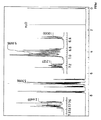
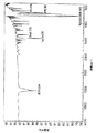
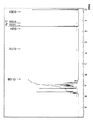
1H−NMRスペクトルを図2に、13C−NMRスペクトルを図3に、赤外線スペクトルを図4に示す。
【0109】
<合成例3>
化合物3(10,10’−ビス−(2−p−ターフェニルイル)−9,9’−ビアンスリル)の合成
合成例1の2−ブロモビフェニルの代わりに、2−ブロモ−P−ターフェニル9.3g を用いて合成を行い、4.0g の目的化合物を得た。この目的物(10,10’−ビス−(2−p−ターフェニルイル)−9,9’−ビアンスリル)の構造式を下記に示す。
【0110】
【化8】
この化合物の質量分析およびNMRスペクトル、赤外吸収スペクトルの測定を行ったところ、目的物と矛盾しないことを確認した。また、ガラス転移温度を測定したところ、154度であった。
1H−NMRスペクトルを図5に示す。
【0112】
<合成例4>
化合物4(10,10’−ビス−(2,5−フェニルフェニル)−9,9’−ビアンスリル)の合成
合成例1の2−ブロモビフェニルの代わりに、1−ブロモ−2,5−ジフェニルベンゼン9.3g を用いて合成を行い、4.0g の目的化合物を得た。この目的物(10,10’−ビス−(2,5−フェニルフェニル)−9,9’−ビアンスリル)の構造式を下記に示す。
【0113】
【化9】
この化合物の質量分析およびNMRスペクトル、赤外吸収スペクトルの測定ヲ行ったところ、目的物と矛盾しないことを確認した。また、ガラス転移温度を測定したところ、145度であった。
1H−NMRスペクトルを図6に、13C−NMRスペクトルを図7に、赤外線スペクトルを図8に示す。
【0115】
<合成例5>
化合物5(10,10’-ビス[-2-(-5-フェニルチエニル-2-イル)フェニル]-9,9’-ビアンスリル)の合成
合成例1の2−ブロモビフェニルの代わりに、2-(-5-フェニルチエニル-2-イル)ブロモベンゼン3.5g を用いて合成を行い、0.9g の目的化合物を得た。得られた目的物(10,10’-ビス[-2-(-5-フェニルチエニル-2-イル)フェニル]-9,9’-ビアンスリル)の構造を下記に示す。
【0116】
【化10】
この黄白色個体の質量分析およびNMRスペクトル、赤外吸収スペクトルの測定を行ったところ、目的物と矛盾しないことを確認した。また、ガラス転移温度を測定したところ、146度であった。
1H−NMRスペクトルを図9に示す。
【0118】
<合成例6>
化合物6(9,9’,10,10’-テトラキス(-2-ビフェニルイル)-2,2’-ビアンスリル)の合成
2−ブロモビフェニル11.4g、ジエチルエーテル50mlとトルエン50m1を混合し、これに1.6Mブチルリチウムのヘキサン溶液30をゆっくり滴下しながら1時間室温で攪拌し、2−リチオビフェニルを調整した。次に、トルエン150m1と2−クロロアントラキノン5.5gの混合物にこのリチオビフェニルをゆっくり滴下し、室温で一昼夜攪拌した。次いで、これに蒸留水100mlを加えさらに1時間攪拌した後、この溶液を濾過し、廬物をメタノールで洗浄した。得られた物を再結晶した後、カラム精製し、9.8g の白色固体としてジオール体を得た。
【0119】
このジオール体9.6g とテトラヒドロフラン400mlを混合し、これに塩化すず25gと塩酸25mlの混合液をゆっくり滴下した。さらに、これを70度のオイルバスで2時間加熱した後冷却し、200mlのトルエンを加え、蒸留水及び炭酸水素ナトリウムで洗浄した。硫酸マグネシウムで乾燥した後、カラム精製と再沈を繰り返し、純白色の2−クロロ−9,10−ジフェニルアントラセン7.1g を得た。
【0120】
次に、2−クロロ−9,10−ジフェニルアントラセン4.5g、Ni(cod)21.8g、DMF100ml、1,5−シクロオクタジエン3ml、2,2’−ビピリジン1gを混合し、60度で20時間反応した後、これをメタノール200m1に加え、さらに2時間攪拌した。この溶液を濾過し、廬物をメタノール、ヘキサン、アセトンで洗浄した後、再結晶およびカラム精製を行い、3g の白色固体を得た。これを昇華精製し、2.8gの黄白色個体を得た。得られた目的物の構造を下記に示す。
【0121】
【化11】
この黄白色個体の質量分析およびNMRスペクトル、赤外吸収スペクトルの測定を行ったところ、目的物と矛盾しないことを確認した。また、ガラス転移温度を測定したところ、166度であった。
【0123】
なお、ガラス上に蒸着して放置したところ半年以上アモルファスの安定な膜を維持した。
【0124】
<合成例7>
化合物7(10,10’-ビス[2-(-5-フェニルチエニル-2-イル)フェニル]-9,9’-ビアンスリル)の合成
乾燥した容器に、2−(5−フェニルチエニル−2−イル)ブロモベンゼン3.5g と、トルエン50mlとジエチルエーテル50mlを加えた後、1.6Mのn−ブチルリチウムのヘキサン溶液7.2mlをゆっくり加え1時間室温で攪拌し、2−(5−フェニルチエニル−2−イル)リチオベンゼンを得た。次に、乾燥した別の容器に10,10’−ビアンスロン2g とトルエン100mlを加えよく撹拌した。この反応液の中に、先に調整した2−(5−フェニルチエニル−2−イル)リチオベンゼンをゆっくり滴下した。室温で20時間攪拌した後、蒸留水40mlを加え、生じた沈殿物を濾別した。この沈殿物を2回洗浄した後、カラム分離を2回行い、再結晶して2.9g の白色固体としてジオール体を得た。
【0125】
次に反応容器に、得られたジオール体2.9g とテトラヒドロフラン400mlに、塩化すず25g と塩酸40mlを混合した溶液をゆっくり滴下した。この反応容器を60℃のオイルバスで2時間撹拌した。この反応溶液に100mlのトルエンを加え、有機層を分離した後、塩酸と蒸留水で洗浄した後、乾燥した。得られた固体を、カラム精製2回(吸着剤:シリカゲル、展開溶媒:トルエン)した後、トルエン/ヘキサン系溶液から再沈し、黄白色の固体1.2g を得た。さらに、この黄白色固体1.2g を昇華精製し0.9g の黄白色固体を得た。得られた目的物(10,10’-ビス[2-(-5-フェニルチエニル-2-イル)フェニル]-9,9’-ビアンスリル)の構造式を下記に示す。
【0126】
【化12】
この黄白色個体の質量分析およびNMRスペクトル、赤外吸収スペクトルの測定を行ったところ、目的物と矛盾しないことを確認した。
【0128】
<実施例1>
厚さ100nmのITO透明電極(陽極)を有するガラス基板を、中性洗剤、アセトン、エタノールを用いて超音波洗浄し、煮沸エタノール中から引き上げて乾燥した。透明電極表面をUV/O3 洗浄した後、真空蒸着装置の基板ホルダーに固定して、チャンバー内を10-4 Pa以下の減圧状態とした。
【0129】
次に、ホール注入層として、減圧状態を保ったまま、N,N’−ジフェニル−N,N’−ビス[N−(4-メチルフェニル)− N−フェニル-(4-アミノフェニル)]−1,1’−ビフェニル−4,4’−ジアミンを蒸着速度0.1nm/secで80nmの厚さに形成した。
【0130】
次いで、減圧状態を保ったまま、ホール輸送層として、N,N’−ジフェニル−N,N’−ビス (1-ナフチル)−1,1’−ジフェニル−4,4’−ジアミンを蒸着速度0.1nm/secで15nmの厚さに形成した。
【0131】
さらに、減圧状態を保ったまま、発光層として、化合物1を蒸着速度0.1nm/secで40nmの厚さに形成した後、電子注入層として、トリス-8-キノリノラトアルミニウムを蒸着速度0.1nm/secで15nmの厚さに形成した。
【0132】
次に、減圧状態を保ったまま、電子注入電極としてLi2Oを蒸着速度0.01nm/secで1nmの厚さに形成した後、配線電極として、Alを蒸着速度2nm/secで200nmの厚さに形成した
【0133】
この有機EL素子に電圧を印加して電流を流したところ、6.0V 、10mA/cm2 で200cd/m2 の発光(発光極大波長λmax =420nm、色度座標(x,y)=(0.10,0.08)が確認された。
【0134】
また、この素子に、50mA/cm2 の一定電流を流し、連続発光させたところ、初期輝度840cd/m2 初期駆動電圧は7.4V となり、140時間後に輝度は半減した。このとき駆動電圧上昇は2.2Vであった。
【0135】
<実施例2>
実施例1において、発光層として上記合成例の化合物1(化6)と下記で示す化合物を、100:3の重量比率で共蒸着する他は同様にして有機EL素子を得た。
【0136】
【化13】
この有機EL素子に電圧を印加して電流を流したところ、5.9V 、10mA/cm2 で1200cd/m2 の発光(発光極大波長λmax =460nm、色度座標(x,y)=(0.17,0.32)が確認された。
【0138】
また、この素子に、50mA/cm2 の一定電流を流し、連続発光させたところ、初期輝度6500cd/m2 初期駆動電圧は7.4V となり、400時間後に輝度は半減した。このとき駆動電圧上昇は2.2Vであった。
【0139】
<実施例3>
実施例1において、発光層として上記合成例の化合物1の代わりに化7と下記で示す化合物を100:3の重量比率で共蒸着する他は同様にして有機EL素子を得た。
【0140】
【化14】
この有機EL素子に電圧を印加して電流を流したところ、6.0V 、10mA/cm2 で400cd/m2 の発光(発光極大波長λmax =420nm、色度座標(x,y)=(0.10,0.10)が確認された。
【0142】
また、この素子に、50mA/cm2 の一定電流を流し、連続発光させたところ、初期輝度2100cd/m2 初期駆動電圧は7.6V となり、250時間後に輝度は半減した。このとき駆動電圧上昇は2.2Vであった。
【0143】
<比較例1>
実施例1において、発光層として化合物1の代わりに10,10’-ビス(2,6’-ジメチルフェニル)-9,9’-ビアンスリルを用いる他は同様にして有機EL素子を得た。
【0144】
この有機EL素子に電圧を印加して電流を流したところ、6.5V 、10mA/cm2 で140cd/m2 の発光(発光極大波長λmax =430 nm、色度座標(x,y)=(0.10,0.10)が確認された。
【0145】
また、この素子に、50mA/cm2 の一定電流を流し、連続発光させたところ、初期輝度650cd/m2 初期駆動電圧は8.0V となり、20時間後に輝度は半減した。このとき駆動電圧上昇は3.0V であった。
【0146】
<比較例2>
実施例2において、発光層として化合物1の代わりに10,10’-ビス(2,6’-ジメチルフェニル)-9,9’-ビアンスリルを用いる他は同様にして有機EL素子を得た。
【0147】
この有機EL素子に電圧を印加して電流を流したところ、6.7V 、10mA/cm2 で869cd/m2 の発光(発光極大波長λmax =460nm、色度座標(x,y)=(0.17,0.32)が確認された。
【0148】
また、この素子に、50mA/cm2 の一定電流を流し、連続発光させたところ、初期輝度4900cd/m2 初期駆動電圧は7.9V となり、50時間後に輝度は半減した。このとき駆動電圧上昇は3.2V であった。
【0149】
【発明の効果】
本発明の有機EL素子用化合物は、結晶性が低く、アモルファス状態の良好な膜を形成することができるので、有機EL素子用化合物、特に青色発光材料や電子注入輸送材料として用いることができる。
【0150】
また、本発明の有機EL素子用化合物を用いた本発明の有機EL素子は電流リークがなく、非発光部分(ダークスポット)の発生・成長がなく、膜中の結晶化が抑制されるので連続発光の信頼性の高い素子となる。特に発光層に用いた場合1万cd/m2 以上の高輝度の青色発光が可能となるだけでなく、十分な発光効率、長寿命を有する。
【図面の簡単な説明】
【図1】本発明のEL素子の構成例を示す側面図である。
【図2】本発明の合成例2の化合物の1H−NMRのスペクトルを示した図である。
【図3】本発明の合成例2の化合物の13C−NMRのスペクトルを示した図である。
【図4】本発明の合成例2の化合物の赤外線スペクトルを示した図である。
【図5】本発明の合成例3の化合物の1H−NMRのスペクトルを示した図である。
【図6】本発明の合成例4の化合物の1H−NMRのスペクトルを示した図である。
【図7】本発明の合成例4の化合物の13C−NMRのスペクトルを示した図である。
【図8】本発明の合成例4の化合物の赤外線スペクトルを示した図である。
【図9】本発明の合成例5の化合物の1H−NMRのスペクトルを示した図である。
【符号の説明】
1 有機EL素子
2 基板
3 陽極
4 ホール注入輸送層
5 発光層
6 電子注入輸送層
7 陰極[0001]
BACKGROUND OF THE INVENTION
The present invention relates to a compound used in an organic EL (electroluminescence) device, and more particularly to an organic compound that is a phenylanthracene derivative and a device that emits light by applying an electric field to a laminated thin film having the compound.
[0002]
[Prior art]
The organic EL element has a configuration in which a thin film containing a fluorescent organic compound is sandwiched between a cathode and an anode, and excitons (excitons) are generated by injecting electrons and holes into the thin film and recombining them. It is an element that emits light by utilizing light emission (fluorescence / phosphorescence) when this exciton is deactivated.
[0003]
The characteristics of organic EL elements are 100 to several thousand cd / m at a low voltage of about 10V.2It is possible to emit surface light with a level of high brightness, and it is possible to emit light from blue to red by selecting the type of fluorescent material, but the problem is that the light emission life is short and the storage durability is inferior. In order to solve these problems, various researches and developments are currently underway.
[0004]
Specifically, as a means of high efficiency and long life, a method of doping a small amount of a fluorescent dye having a high fluorescence quantum yield (JP 05-198377 A, JP 07-135077 A, etc.), A method for obtaining a high-efficiency device by using a bipolar light-emitting layer in which a hole transporting material and an electron transporting material are mixed as a light-emitting layer, expanding a carrier recombination region, and improving a recombination probability (
[0005]
However, when the doping method is used, many of the fluorescent dyes that serve as dopants have strong concentration quenching properties, and it is necessary to control the dopant concentration at a level of several percent in terms of weight ratio when forming an element. In general, an EL element using a low molecular compound is often produced by a vacuum deposition method, and such precise concentration control is not easy and causes a narrow manufacturing margin. Furthermore, in order to obtain blue light emission by doping, a dopant having a large energy gap is emitted, so that materials that can serve as a host are limited, and selection of a combination of dopants becomes difficult.
[0006]
In addition, even when a bipolar light emitting layer is used, the recombination probability is improved, but in order to finally extract energy as light, it is often necessary to use a dopant having a high fluorescence quantum yield. In addition, when such a bipolar mixed light emitting layer is used, there is a drawback that the drive voltage becomes relatively high.
[0007]
On the other hand, the present inventors have disclosed a high-luminance light-emitting element using a phenylanthracene derivative with little physical change, photochemical change, and electrochemical change in Japanese Patent Application Laid-Open No. 08-12600. In the low blue region, sufficient efficiency has not been obtained, and further improvement in characteristics is required for practical use in terms of light emission life and durability.
[0008]
[Problems to be solved by the invention]
An object of the present invention is to provide a novel compound for an organic EL device as an optical / electronic functional material with little physical change, photochemical change, and electrochemical change, and using this organic EL device compound, extremely high reliability is provided. And an organic EL element having various emission colors having luminous efficiency. In particular, using an organic thin film formed by vapor deposition of a compound with a large molecular weight, high reliability with reduced drive voltage and reduced brightness, current leakage, and the appearance / growth of non-light emitting parts during device operation It is to realize a high-luminance light emitting element.
[0009]
[Means for Solving the Problems]
Such an object is achieved by the present inventions (1) to (13) below.
(1) A compound for an organic EL device, which is a phenylanthracene derivative represented by the following formula (I).
Formula (I)
A1-LA2
[In Formula (I), A1And A2Each represents a mono (ortho-substituted phenyl) anthryl group or a di (ortho-substituted phenyl) anthryl group, which may be the same or different. Ortho-substituted phenyl isAn unsubstituted aryl group having 42 or less carbon atoms, an alkyl group having 12 or less carbon atoms, an alkoxy group, an allyloxy group, an amino group, a cyano group, or a nitro group.Substituted or unsubstituted heterocyclic aryl group,Or, Unsubstituted aryl group, alkyl group, alkoxy group, allyloxy group, amino group, cyano group, nitro groupSubstituted or unsubstituted arylethenyl group,soA phenyl group substituted at the ortho position.The aryl group represents an aromatic hydrocarbon ring group, the heterocyclic aryl group represents an aromatic heterocyclic group containing O, N or S, and the aryl group constituting the arylethenyl group represents an aromatic hydrocarbon ring group. To express.L is a single bond orNoRepresents a substituted arylene group,NothingThe substituted arylene group isTwo or more unsubstituted arylene groups may be directly linked,Alkylene group,-O-,-S- or -NR- (where R is an alkyl group orNoRepresents a substituted aryl group)It may be connected by intervening. The arylene group represents an aromatic hydrocarbon ring group.]
(2) The compound for organic EL element of the above (1) represented by the following chemical formula 1 or
[0010]
[Chemical Formula 3]
[Formula 4]
[In Chemical Formula 1, Ar1~ Ar4Is a hydrogen atom,An unsubstituted aryl group having 42 or less carbon atoms, an alkyl group having 12 or less carbon atoms, an alkoxy group, an allyloxy group, an amino group, a cyano group, or a nitro group.Substituted or unsubstituted heterocyclic aryl group,Or, Unsubstituted aryl group, alkyl group, alkoxy group, allyloxy group, amino group, cyano group, nitro groupRepresents a substituted or unsubstituted arylethenyl groupThe
Ar1And Ar2, Ar3And Ar4At least one ofAn unsubstituted aryl group having 42 or less carbon atoms, an alkyl group having 12 or less carbon atoms, an alkoxy group, an allyloxy group, an amino group, a cyano group, or a nitro group.Substituted or unsubstituted heterocyclic aryl group,Or, Unsubstituted aryl group, alkyl group, alkoxy group, allyloxy group, amino group, cyano group, nitro groupA substituted or unsubstituted arylethenyl group;
R1And R2Are each an alkyl group,Phenyl group, tolyl groupA substituted or unsubstituted aryl group,In unsubstituted aryl group, alkyl group, alkoxy group, allyloxy group, amino group, cyano group, nitro groupIt represents a substituted or unsubstituted arylethenyl group, an alkoxy group, or an amino group, which may be the same or different.
r1 and r2 each represent an integer of 0 or 1-3, and when r1 and r2 are each an integer of 2 or more, R11And R2Each may be the same or different. R3Is an alkyl group orPhenyl group, tolyl groupA substituted or unsubstituted aryl group is represented, and r3 represents 0 or an integer of 1 to 3, respectively. When r3 is an integer of 2 or more, R3May be the same or different.
L1Is a single bond orNoRepresents a substituted arylene group,NothingThe substituted arylene group isTwo or more unsubstituted arylene groups may be directly linked,Alkylene group,-O-,-S- or -NR- (where R is an alkyl group orNoRepresents a substituted aryl group. )It may be connected by intervening.
In
Ar5And Ar6At least one ofAn unsubstituted aryl group having 42 or less carbon atoms, an alkyl group having 12 or less carbon atoms, an alkoxy group, an allyloxy group, an amino group, a cyano group, or a nitro group.Substituted or unsubstituted heterocyclic aryl group,Or, Unsubstituted aryl group, alkyl group, alkoxy group, allyloxy group, amino group, cyano group, nitro groupA substituted or unsubstituted arylethenyl group;
R4Are each an alkyl group,Phenyl group, tolyl groupA substituted or unsubstituted aryl group,In unsubstituted aryl group, alkyl group, alkoxy group, allyloxy group, amino group, cyano group, nitro groupIt represents a substituted or unsubstituted arylethenyl group, an alkoxy group, or an amino group, which may be the same or different. r4 represents an integer of 0 or 1 to 3, and when r4 is an integer of 2 or more, R44Each may be the same or different. R5Is an alkyl group,Or, Phenyl group, tolyl groupA substituted or unsubstituted aryl group is represented, and r5 represents 0 or an integer of 1 to 4, respectively. When r5 is an integer of 2 or more, R5May be the same or different.
L2Is a single bond orNoRepresents a substituted arylene group,NothingThe substituted arylene group isTwo or more unsubstituted arylene groups may be directly linked,Alkylene group,-O-, -S- or -NR- (where R is an alkyl group orNoRepresents a substituted aryl group. )It may be connected by intervening.]
(3) In Formula 1, Ar1And Ar2, Ar3And Ar4At least one ofIsThe compound for an organic EL device according to the above (2), which is a thylyl group, a phenylstyryl group, a diphenylstyryl group, a thienyl group, a methylthienyl group, a phenylthienyl group or a phenylbithienyl group.
(4) In the
(5) In the chemical formula 1, L 1 Is a compound for an organic EL device according to the above (2), which is a single bond.
(6) In the
(7) An organic EL device having at least one organic compound layer containing the compound for organic EL devices of (1) above.
(8) The organic EL device according to (7), wherein the organic compound layer containing the compound for organic EL device is a light emitting layer.
(9) The organic EL device according to (8), further comprising at least one hole injection layer, at least one hole transport layer, and at least one electron injection transport layer.
(10) The organic EL device according to (8), further comprising at least one hole injection layer, at least one hole transport layer, at least one electron transport layer, and at least one electron injection layer. .
(11) The organic EL device according to (7), wherein the organic compound layer containing the compound for organic EL device is an electron injecting and transporting layer, and further has a light emitting layer.
(12) It has at least one light emitting layer, and this light emitting layer is a mixed layer of an electron injecting and transporting compound and a hole injecting and transporting compound, and this mixed layer contains the compound for an organic EL device. (7) Organic EL element.
(13) The organic EL device according to (12), wherein the electron injecting / transporting compound is the compound for an organic EL device, and the hole injecting / transporting compound is an amine or a styrylamine compound.
[0013]
[Action]
The organic EL device of the present invention uses the compound represented by the above formula (I), preferably the
[0014]
In particular, the above compound introduces an aryl group, a heterocyclic aryl group or an arylethenyl group at the 2-position or 6-position of the phenyl group (ortho position relative to the bonding position to the anthracene ring). Since there is almost no intermolecular interaction such as plexes, and there is very little reduction in color purity and efficiency, an organic EL device with high reliability and light emission efficiency can be obtained.
[0015]
Further, when the ortho-position substituent extends as a π-electron conjugated system like the compound of the present invention, the carrier transport property can be improved and the driving voltage of the device can be lowered.
[0016]
Since the vapor-deposited film of the above compound is in a stable amorphous state, the thin film has excellent physical properties and uniform light emission is possible. In addition, it is stable for over a year in the atmosphere and does not cause crystallization.
[0017]
In addition, a stable amorphous thin film can be formed even in a wet film forming process such as spin coating that dissolves in chloroform or the like.
[0018]
The organic EL device of the present invention emits light efficiently at a low driving voltage.
[0019]
In addition, the light emission maximum wavelength of the organic EL element of this invention is about 400-700 nm, and it light-emits efficiently especially in the 400-500 nm area | region.
[0020]
DETAILED DESCRIPTION OF THE INVENTION
Hereinafter, a specific configuration of the present invention will be described in detail.
The phenylanthracene derivative of the present invention is represented by the formula (I). When formula (I) is described, A1And A2Each represents a mono (ortho-substituted phenyl) anthryl group or a di (ortho-substituted phenyl) phenylanthryl group, which may be the same or different.
[0021]
A1, A2The mono (ortho-substituted phenyl) phenylanthryl group or di (ortho-substituted phenyl) phenylanthryl group represented by the formula: is in the 2-position or 6-position of the phenyl group (ortho position relative to the bonding position to the anthracene ring), Those having an aryl group, a heterocyclic aryl group or an arylethenyl group. Further, it may have a substituent other than the ortho position, and examples of the substituent in the case of having a substituent include an alkyl group, an aryl group, an arylethenyl group, an alkoxy group, an amino group, etc. These substituents may be further substituted. These substituents will be described later.
[0022]
Moreover, it is preferable that the bonding position of the phenyl group in the anthracene ring is the 9th or 10th position of the anthracene ring.
[0023]
In the formula (I), L represents a single bond or a divalent group, and the divalent group represented by L is preferably an arylene group in which an alkylene group or the like may be interposed. Such an arylene group will be described later.
[0024]
Among the phenylanthracene derivatives represented by the formula (I), those represented by
[0025]
Ar1~ ArFourAnd R1~ RThreeAs the aryl group represented by the formula, those having 6 to 20 carbon atoms are preferable, and further, those having a substituent such as a phenyl group and a tolyl group may be used. Specific examples include a phenyl group, (o-, m-, p-) tolyl group, pyrenyl group, naphthyl group, anthryl group, biphenyl group, phenylanthryl group, and tolylanthryl group.
[0026]
Ar1~ ArFourAs the heterocyclic aryl group represented by the formula, furyl group, benzofuryl group, thienyl group, benzothienyl group, pyrrolyl group, N-allylpyrrolyl group, indolyl group, pyridyl group, bipyridyl group, quinolyl group, quinoxalyl group, oxazole group, A benzoxazole group, an oxadiazole group, a thiazole group, a benzothiazole group, a thiadiazole group, an imidazole group and the like are preferable, and further, an aryl group having 42 or less carbon atoms, an alkyl group having 12 or less carbon atoms, an alkoxy group, an allyloxy group, It may have a substituent such as an amino group, a cyano group, or a nitro group. Specifically, a phenyl group, (o-, m-, p-) biphenyl group, (1,2) naphthyl group, methyl group, ethyl group, propyl group, butyl group, methoxy group, ethoxy Group, phenoxy group, (o-, m-, p-) tolyl group and the like.
[0027]
Ar1~ ArFour, R1And R2As the arylethenyl group represented by, 2-phenylethenyl group, 2,2-diphenylethenyl group and the like are preferable, and further aryl group, alkyl group, alkoxy group, allyloxy group, amino group, cyano group, It may have a substituent such as a nitro group. Specifically, phenyl group, (o-, m-, p-) biphenyl group, (1,2) naphthyl group, methyl group, ethyl group, propyl group, butyl group, methoxy group, ethoxy group, phenoxy group, ( o-, m-, p-) tolyl groups and the like.
[0028]
R1~ RThreeThe alkyl group represented by may be linear or branched, and is preferably a substituted or unsubstituted alkyl group having 1 to 10 carbon atoms and more preferably 1 to 4 carbon atoms. In particular, an unsubstituted alkyl group having 1 to 4 carbon atoms is preferable, and specifically, a methyl group, an ethyl group, a (n-, i-) propyl group, (n-, i-, s-, t-) butyl. Groups and the like.
[0029]
R1And R2As the alkoxy group represented by formula (1), an alkyl group having 1 to 6 carbon atoms is preferable, and specific examples include a methoxy group and an ethoxy group. The alkoxy group may be further substituted.
[0030]
R1And R2The amino group represented by may be unsubstituted or have a substituent, but preferably has a substituent. In this case, examples of the substituent include an alkyl group (methyl group, ethyl group, etc.), aryl Group (phenyl group etc.) etc. are mentioned. Specific examples include a diethylamino group, a diphenylamino group, and a di (m-tolyl) amino group.
[0031]
In
[0032]
In
[0033]
In
[0034]
In
[0035]
L1The arylene group represented by may be a group in which two or more arylene groups are linked via an alkylene group, —O—, —S— or —NR—. Here, R represents an alkyl group or an aryl group. Examples of the alkyl group include a methyl group and an ethyl group, and examples of the aryl group include a phenyl group. Among them, an aryl group is preferable, and in addition to the above phenyl group, A1, A2Furthermore, A may be added to the phenyl group.1Or A2May be substituted.
[0036]
The alkylene group is preferably a methylene group or an ethylene group. Specific examples of such an arylene group are shown below.
[0037]
[Chemical formula 5]
Next, the
[0039]
Moreover, in
[0040]
In
[0041]
Although the compound represented by
[0042]
[Table 1]
[Table 2]
[Table 3]
[Table 4]
[Table 5]
[Table 6]
[Table 7]
[Table 8]
[Table 9]
[Table 10]
[Table 11]
[Table 12]
[Table 13]
[Table 14]
[Table 15]
[Table 16]
[Table 17]
[Table 18]
[Table 19]
[Table 20]
[Table 21]
[Table 22]
[Table 23]
[Table 24]
[Table 25]
[Table 26]
[Table 27]
[Table 28]
[Table 29]
[Table 30]
The compound for organic EL devices which is the phenylanthracene derivative of the present invention (hereinafter also referred to as “the compound of the present invention”)
(1) A halogenated arylanthracene compound is converted to Ni (cod)2Coupling with [cod: 1,5-cyclooctadiene] or Grignard aryl dihalide to form NiCl2(Dppe) [dppe: diphenylphosphinoethane], NiCl2(Dppp) [dppp: diphenylphosphinopropane], a method of cross-coupling using a Ni complex or the like,
(2) A method of cross-coupling an aryl boronate and a halogenated arylanthracene compound using a Pd complex or the like,
(3) a method of cross-coupling by reaction and reduction of anthraquinone, benzoquinone, phenylanthrone or bianthrone with a Grignard aryl or a lithiated aryl,
Etc.
[0073]
The compound thus obtained is elemental analysis, mass spectrometry, infrared absorption spectrum,1H or13C nuclear magnetic resonance absorption (NMR) spectra can be identified.
[0074]
The phenylanthracene derivative of the present invention has a molecular weight of about 400 to 2000, more preferably about 400 to 1000, a high melting point of 200 to 500 ° C., 80 to 250 ° C., further 100 to 250 ° C., and more It exhibits a glass transition temperature (Tg) of 130 to 250 ° C., particularly 150 to 250 ° C. Accordingly, a smooth and good film in an amorphous state that is transparent and stable even at room temperature or higher is formed by ordinary vacuum deposition or the like, and the good film state is maintained for a long period of time.
[0075]
The organic EL device of the present invention (hereinafter also referred to as “EL device”) has at least one organic compound layer, and at least one organic compound layer contains the compound of the present invention. A configuration example of the organic EL element of the present invention is shown in FIG. The organic EL element shown in the figure has an
[0076]
The light emitting layer has a hole and electron injection function, a transport function thereof, and a function of generating excitons by recombination of holes and electrons. The hole injection / transport layer has a function of facilitating the injection of holes from the anode, a function of transporting holes, and a function of hindering the transport of electrons, and the electron injection / transport layer facilitates the injection of electrons from the cathode. These layers have a function, a function of transporting electrons, and a function of preventing the transport of holes, and these layers increase and confine holes and electrons injected into the light emitting layer, optimize the recombination region, and improve the luminous efficiency. To improve. The electron injecting and transporting layer and the hole injecting and transporting layer are provided as necessary in consideration of the height of each function of the electron injection, electron transport, hole injection, and hole transport of the compound used for the light emitting layer. For example, when the hole injecting and transporting function or electron injecting and transporting function of a compound used in the light emitting layer is high, the light emitting layer is not provided with the hole injecting and transporting layer or the electron injecting and transporting layer without providing the hole injecting and transporting layer or the electron injecting and transporting layer. It can be set as the structure which serves also. In some cases, neither the hole injection transport layer nor the electron injection transport layer may be provided. Further, each of the hole injecting and transporting layer and the electron injecting and transporting layer may be provided with a layer having an injection function and a layer having a transport function.
[0077]
Since the compound of the present invention is a relatively neutral compound, it is preferably used in the light emitting layer, but can also be applied to a hole injecting and transporting layer and an electron injecting and transporting layer.
[0078]
In addition, the recombination region and light emitting region can be controlled by controlling the film thickness while considering the carrier mobility and carrier density (determined by ionization potential and electron affinity) of the light emitting layer, electron injecting and transporting layer, and hole injecting and transporting layer to be combined. Can be designed freely, and it is possible to design the emission color, control the emission luminance and emission spectrum by the interference effect of both electrodes, and control the spatial distribution of emission.
[0079]
The case where the compound of the present invention is used for the light emitting layer will be described. In addition to the compound of the present invention, other fluorescent materials may be used for the light-emitting layer. Examples of other fluorescent materials include compounds disclosed in JP-A-63-264692, for example, Quinacridone, styryl dyes, aromatic hydrocarbons such as rubrene, diphenylisobenzofuran and the like, or tertiary amines and other compounds. The content of such a fluorescent substance is preferably 10 mol% or less of the compound of the present invention. By appropriately selecting and adding such a compound, emitted light can be shifted to the long wavelength side.
[0080]
When the compound of the present invention is used for the light emitting layer, the hole injection transport layer and the electron injection transport layer include various organic compounds used in ordinary organic EL devices, such as JP-A 63-295695, JP-A Various organic compounds described in JP-A-2-191694, JP-A-3-792 and the like can be used. For example, an aromatic tertiary amine, a hydrazone derivative, a carbazole derivative, a triazole derivative, an imidazole derivative, or the like can be used for the hole injecting and transporting layer, and an organometallic complex derivative such as aluminum quinolinol is used for the electron injecting and transporting layer. Oxadiazole derivatives, pyridine derivatives, pyrimidine derivatives, quinoline derivatives, quinoxaline derivatives, diphenylquinone derivatives, perylene derivatives, fluorene derivatives, and the like can be used.
[0081]
When the hole injecting and transporting layer is divided into the hole injecting layer and the hole transporting layer, a preferred combination can be selected from the compounds for the hole injecting and transporting layer. At this time, it is preferable to laminate in order of a compound layer having a small ionization potential from the anode (ITO or the like) side. Further, it is preferable to use a compound having a good thin film property on the anode surface. Such a stacking order is the same when two or more hole injecting and transporting layers are provided. By adopting such a stacking order, the drive voltage is lowered, and the occurrence of current leakage and the generation / growth of dark spots can be prevented. In addition, in the case of elementization, since vapor deposition is used, a thin film of about 1 to 10 nm can be made uniform and pinhole-free, so that the ion injection potential is small in the hole injection layer and the visible portion has absorption. Even if such a compound is used, it is possible to prevent a decrease in efficiency due to a change in color tone of light emission or reabsorption.
[0082]
When the electron injecting and transporting layer is divided into an electron injecting layer and an electron transporting layer, a preferred combination can be selected from the compounds for the electron injecting and transporting layer. At this time, it is preferable to laminate in the order of the layer of the compound having a large electron affinity value from the cathode side. Such a stacking order is the same when two or more electron injecting and transporting layers are provided.
[0083]
In the present invention, the light emitting layer is preferably a mixed layer of an electron injecting and transporting compound and a hole injecting and transporting compound. And the compound of this invention is contained in such a mixed layer. Since the compound of the present invention is usually contained as a fluorescent substance, more specifically, when the compound of the present invention is an electron injection / transport compound, another hole injection / transport compound may be further added. Preferably, when the compound of the present invention is a hole injecting and transporting compound, it is preferable to add another electron injecting and transporting compound. In this case, as a particularly preferred combination, the compound of the present invention is used as the electron injecting and transporting compound, and the amine or styrylamine compound is used as the hole injecting and transporting compound. The mixing ratio of the electron injecting and transporting compound and the hole injecting and transporting compound in the above mixed layer depends on the carrier mobility and the carrier concentration of the material to be used. Hole injection / transport compoundIt is preferably 5:95 to 95: 5, and particularly preferably 10:90 to 90:10. Furthermore, 20:80 to 20:80It is preferable that In addition, the thickness of the mixed layer is preferably less than the thickness of the organic compound from one molecular layer.
[0084]
The electron injecting and transporting compound to be used for mixing is selected from the above compounds for the electron injecting and transporting layer, and the hole injecting and transporting compound is selected from the above compounds for the hole injecting and transporting layer. it can. In some cases, the compounds of the present invention may be selected and used. Furthermore, in the mixed layer, each of the electron injecting and transporting compound and the hole injecting and transporting compound may be used alone or in combination of two or more. The mixed layer may be doped with the compound of the present invention or another fluorescent substance in order to increase the emission intensity.
[0085]
Further, a mixed layer of another electron injecting and transporting compound and another hole injecting and transporting compound may be used, and such a mixed layer may be used by doping the compound of the present invention.
[0086]
By applying such a mixed layer to an EL element, the stability of the element is improved.
[0087]
The compound of the present invention is also preferably used for an electron injecting and transporting layer. In this case, the fluorescent substance used for the light emitting layer is preferably a substance having fluorescence having a wavelength longer than or comparable to that of the compound of the present invention. For example, the fluorescent material that can be used in combination with the compound of the present invention in the light emitting layer can be selected and used. Moreover, the compound of this invention can be used also for a light emitting layer in such a structure. Moreover, the compound of this invention can be used also for the light emitting layer which served as the electron injection transport layer. In the case of an electron injecting and transporting layer, a metal, metal halide or metal oxide having a low work function such as Li, Na, K, or Cs is doped at or near the electrode interface in order to improve the electron carrier density. May be.
[0088]
The compound of the present invention can be used for a hole injecting and transporting layer.
[0089]
When the compound of the present invention is used for the hole injecting and transporting layer, the fluorescent material used for the light emitting layer may be selected from those having a longer wavelength of fluorescence than the compound of the present invention. What is necessary is just to select suitably from 1 or more types of the fluorescent substance used together with this compound. In such a case, the compound of this invention can be used also for a light emitting layer. In the case of a hole injecting and transporting layer, a hole generating dopant such as a quaternary amine may be doped on the electrode interface or in the vicinity of the interface in order to improve the hole carrier density.
[0090]
In addition, in the above, when using another fluorescent substance mainly for a light emitting layer, you may add and use the compound of this invention 10 mol% or less as a fluorescent substance together.
[0091]
The thickness of the light emitting layer, the thickness of the hole injecting and transporting layer, and the thickness of the electron injecting and transporting layer are not particularly limited and vary depending on the forming method, but are usually about 5 to 1000 nm, and particularly preferably 8 to 200 nm. .
[0092]
The thickness of the hole injecting and transporting layer and the thickness of the electron injecting and transporting layer may be about the same as the thickness of the light emitting layer or about 1/10 to 10 times depending on the design of the recombination / light emitting region. When the injection layer and the transport layer for electrons or holes are separated, the injection layer is preferably 1 nm or more, and the transport layer is preferably 20 nm or more. In this case, the upper limit of the thickness of the injection layer and the transport layer is usually about 100 nm for the injection layer and about 1000 nm for the transport layer.
[0093]
For the cathode, it is preferable to use a material having a low work function, such as Li, Na, Mg, Al, Ag, In, or an alloy containing one or more of these materials. Further, the cathode preferably has fine crystal grains, and particularly preferably in an amorphous state. The thickness of the cathode is preferably about 10 to 1000 nm.
[0094]
In order to cause the EL element to emit light, at least one of the electrodes needs to be transparent or translucent, and as described above, the cathode material is limited, so that the transmittance of emitted light is preferably 80% or more. It is preferable to determine the material and thickness of the anode so that Specifically, for example, ITO, SnO2Ni, Au, Pt, Pd, polypyrrole doped with a dopant, or the like is preferably used for the anode. The thickness of the anode is preferably about 10 to 500 nm. Further, in order to improve the reliability of the element, it is necessary that the driving voltage is low, but preferable examples include ITO of about 10 to 30Ω / □ or 10Ω / □ or less (usually 5 to 10Ω / □).
[0095]
The substrate material is not particularly limited, but in the illustrated example, a transparent or translucent material such as glass or resin is used to extract emitted light from the substrate side. Further, the emission color may be controlled by using a color filter film or a dielectric reflection film on the substrate.
[0096]
Note that when an opaque material is used for the substrate, the stacking order shown in FIG. 1 may be reversed.
[0097]
Next, the manufacturing method of the organic EL element of this invention is demonstrated.
The cathode and the anode are preferably formed by vapor deposition such as vapor deposition or sputtering.
[0098]
In forming the hole injecting and transporting layer, the light emitting layer, and the electron injecting and transporting layer, it is preferable to use a vacuum deposition method because a homogeneous thin film can be formed. When the vacuum deposition method is used, a homogeneous thin film having an amorphous state or a crystal grain size of 0.2 μm or less (usually 0.01 μm or more) can be obtained. If the crystal grain size exceeds 0.2 μm, non-uniform light emission occurs, the drive voltage of the device must be increased, and the charge injection efficiency is also significantly reduced.
[0099]
The conditions for vacuum deposition are not particularly limited, but 10-Five The degree of vacuum is less than Torr, and the deposition rate is preferably about 0.1 to 1 nm / sec. Moreover, it is preferable to form each layer continuously in a vacuum. If formed continuously in a vacuum, impurities can be prevented from adsorbing to the interface of each layer, so that high characteristics can be obtained. In addition, the driving voltage of the element can be lowered.
[0100]
In the case of using a vacuum deposition method for forming each of these layers, when a plurality of compounds are contained in one layer, the temperature of each boat containing the compounds is individually controlled and co-deposited while being monitored with a crystal oscillator thickness meter. It is preferable.
[0101]
The EL element of the present invention is usually used as a direct current drive type EL element, but can be alternating current driven or pulse driven. The applied voltage is usually about 2 to 20V.
[0102]
【Example】
Hereinafter, specific examples of the present invention will be shown together with comparative examples, and the present invention will be described in more detail.
<Synthesis Example 1>
Synthesis of Compound 1 (10,10′-bis (2-biphenylyl) -9,9′-bianthryl) 7.8 g of 2-bromobiphenyl, 50 ml of diethyl ether and 50 ml of toluene were mixed with 1.6 M butyllithium. 2-Lithiobiphenyl was prepared by stirring at room temperature for 1 hour while slowly adding 20.4 ml of a hexane solution. Next, this lithiobiphenyl was slowly added dropwise to a mixture of 150 ml of toluene and 4 g of Beanthrone and stirred at room temperature for a whole day and night. Next, 100 ml of distilled water was added thereto, and the mixture was further stirred for 1 hour. The solution was filtered, and the sediment was washed with toluene and methanol. The obtained product was recrystallized from tetrahydrofuran and toluene and purified by column to obtain 4.3 g of a diol as a white solid.
[0103]
4 g of this diol and 400 ml of tetrahydrofuran were placed in a flask, and a solution prepared by mixing 25 g of tin chloride and 25 ml of hydrochloric acid was slowly added dropwise. The flask was heated in a 70 ° oil bath for 2 hours and then cooled, 200 ml of toluene was added, and the mixture was washed with distilled water and sodium hydrogen carbonate. After drying with magnesium sulfate, column purification and reprecipitation were repeated to obtain 3.7 g of a pale yellowish white solid. Sublimation purification of 3.0 g of this pale yellowish white solid yielded 2.8 g of a yellowish white solid. The structure of this target product (10,10'-bis (2-biphenylyl) -9,9'-bianthryl) is shown below.
[0104]
[Chemical 6]
Mass spectrometry, NMR spectrum, and infrared absorption spectrum of this yellowish white solid were measured and confirmed to be consistent with the target product. Moreover, it was 144 degree | times when the glass transition temperature was measured.
[0106]
<Synthesis Example 2>
Synthesis of Compound 2 (10,10'-bis (2,6-diphenylphenyl) -9,9'-bianthryl)
Synthesis was performed using 9.3 g of 1-bromo-2,6-diphenylbenzene instead of 2-bromobiphenyl of Synthesis Example 1 to obtain 4.0 g of the target compound. The structure of the target product (10,10'-bis (2,6-diphenylphenyl) -9,9'-bianthryl) is shown below.
[0107]
[Chemical 7]
Mass spectrometry, NMR spectrum and infrared absorption spectrum of this compound were measured, and it was confirmed that it was consistent with the target product. Moreover, melting | fusing point was 340 degreeC and the glass transition temperature was 166 degree | times.
1The H-NMR spectrum is shown in FIG.13The C-NMR spectrum is shown in FIG. 3, and the infrared spectrum is shown in FIG.
[0109]
<Synthesis Example 3>
Synthesis of Compound 3 (10,10'-bis- (2-p-terphenylyl) -9,9'-bianthryl)
Synthesis was performed using 9.3 g of 2-bromo-P-terphenyl instead of 2-bromobiphenyl of Synthesis Example 1 to obtain 4.0 g of the target compound. The structural formula of this target product (10,10'-bis- (2-p-terphenylyl) -9,9'-bianthryl) is shown below.
[0110]
[Chemical 8]
Mass spectrometry, NMR spectrum and infrared absorption spectrum of this compound were measured, and it was confirmed that it was consistent with the target product. The glass transition temperature was measured and found to be 154 degrees.
1The H-NMR spectrum is shown in FIG.
[0112]
<Synthesis Example 4>
Synthesis of Compound 4 (10,10'-bis- (2,5-phenylphenyl) -9,9'-bianthryl)
Synthesis was carried out using 9.3 g of 1-bromo-2,5-diphenylbenzene instead of 2-bromobiphenyl in Synthesis Example 1 to obtain 4.0 g of the desired compound. The structural formula of this target product (10,10'-bis- (2,5-phenylphenyl) -9,9'-bianthryl) is shown below.
[0113]
[Chemical 9]
Mass spectrometry, NMR spectrum and infrared absorption spectrum of this compound were measured, and it was confirmed that it was consistent with the target product. Moreover, it was 145 degree | times when the glass transition temperature was measured.
1The H-NMR spectrum is shown in FIG.13A C-NMR spectrum is shown in FIG. 7, and an infrared spectrum is shown in FIG.
[0115]
<Synthesis Example 5>
Synthesis of Compound 5 (10,10'-bis [-2-(-5-phenylthienyl-2-yl) phenyl] -9,9'-bianthryl)
Synthesis was performed using 3.5 g of 2-(-5-phenylthienyl-2-yl) bromobenzene instead of 2-bromobiphenyl of Synthesis Example 1 to obtain 0.9 g of the target compound. The structure of the obtained target product (10,10'-bis [-2-(-5-phenylthienyl-2-yl) phenyl] -9,9'-bianthryl) is shown below.
[0116]
[Chemical Formula 10]
Mass spectrometry, NMR spectrum, and infrared absorption spectrum of this yellowish white solid were measured and confirmed to be consistent with the target product. Moreover, it was 146 degree | times when the glass transition temperature was measured.
1The H-NMR spectrum is shown in FIG.
[0118]
<Synthesis Example 6>
Compound6Synthesis of (9,9 ', 10,10'-tetrakis (-2-biphenylyl) -2,2'-bianthryl)
2-Lithobibiphenyl was prepared by mixing 11.4 g of 2-bromobiphenyl, 50 ml of diethyl ether and 50 ml of toluene and stirring at room temperature for 1 hour while slowly dropping a 1.6M butyllithium hexane solution 30 thereto. Next, this lithiobiphenyl was slowly added dropwise to a mixture of 150 ml of toluene and 5.5 g of 2-chloroanthraquinone, and stirred at room temperature for a whole day and night. Next, 100 ml of distilled water was added thereto, and the mixture was further stirred for 1 hour, and then the solution was filtered and the sediment was washed with methanol. The obtained product was recrystallized and purified by column to obtain diol as 9.8 g of white solid.
[0119]
9.6 g of this diol and 400 ml of tetrahydrofuran were mixed, and a mixed solution of 25 g of tin chloride and 25 ml of hydrochloric acid was slowly added dropwise thereto. Further, this was heated in an oil bath at 70 ° C. for 2 hours and then cooled, 200 ml of toluene was added, and the mixture was washed with distilled water and sodium bicarbonate. After drying with magnesium sulfate, column purification and reprecipitation were repeated to obtain 7.1 g of pure white 2-chloro-9,10-diphenylanthracene.
[0120]
Next, 4.5 g of 2-chloro-9,10-diphenylanthracene, 21.8 g of Ni (cod), 100 ml of DMF, 3 ml of 1,5-cyclooctadiene, and 1 g of 2,2′-bipyridine were mixed at 60 degrees. After reacting for 20 hours, this was added to 200 ml of methanol and further stirred for 2 hours. This solution was filtered, and the residue was washed with methanol, hexane, and acetone, and then recrystallized and column purified to obtain 3 g of a white solid. This was purified by sublimation to obtain 2.8 g of a yellowish white solid. The structure of the obtained target product is shown below.
[0121]
Embedded image
Mass spectrometry, NMR spectrum, and infrared absorption spectrum of this yellowish white solid were measured and confirmed to be consistent with the target product. Moreover, it was 166 degree | times when the glass transition temperature was measured.
[0123]
In addition, when deposited on glass and allowed to stand, an amorphous stable film was maintained for more than half a year.
[0124]
<Synthesis Example 7>
Synthesis of Compound 7 (10,10'-bis [2-(-5-phenylthienyl-2-yl) phenyl] -9,9'-bianthryl)
After adding 3.5 g of 2- (5-phenylthienyl-2-yl) bromobenzene, 50 ml of toluene and 50 ml of diethyl ether to a dry container, 7.2 ml of 1.6M n-butyllithium in hexane was added. Slowly added and stirred at room temperature for 1 hour to obtain 2- (5-phenylthienyl-2-yl) lithiobenzene. Next, 2 g of 10,10'-Bienthrone and 100 ml of toluene were added to another dry container and stirred well. Into this reaction liquid, 2- (5-phenylthienyl-2-yl) lithiobenzene prepared previously was slowly added dropwise. After stirring at room temperature for 20 hours, 40 ml of distilled water was added and the resulting precipitate was filtered off. This precipitate was washed twice, followed by column separation twice and recrystallization to obtain diol as a white solid of 2.9 g.
[0125]
Next, a solution obtained by mixing 2.9 g of the obtained diol compound and 400 ml of tetrahydrofuran with 25 g of tin chloride and 40 ml of hydrochloric acid was slowly added dropwise to the reaction vessel. The reaction vessel was stirred in an oil bath at 60 ° C. for 2 hours. 100 ml of toluene was added to the reaction solution, the organic layer was separated, washed with hydrochloric acid and distilled water, and dried. The obtained solid was subjected to column purification twice (adsorbent: silica gel, developing solvent: toluene) and then reprecipitated from a toluene / hexane system solution to obtain 1.2 g of a yellowish white solid. Further, 1.2 g of this yellowish white solid was purified by sublimation to obtain 0.9 g of a yellowish white solid. The structural formula of the obtained target product (10,10'-bis [2-(-5-phenylthienyl-2-yl) phenyl] -9,9'-bianthryl) is shown below.
[0126]
Embedded image
Mass spectrometry, NMR spectrum, and infrared absorption spectrum of this yellowish white solid were measured and confirmed to be consistent with the target product.
[0128]
<Example 1>
A glass substrate having an ITO transparent electrode (anode) with a thickness of 100 nm was subjected to ultrasonic cleaning using a neutral detergent, acetone, and ethanol, and then pulled up from boiling ethanol and dried. UV / O on transparent electrode surfaceThreeAfter cleaning, it is fixed to the substrate holder of the vacuum evaporation system, and the inside of the chamber is 10-Four The pressure was reduced to Pa or lower.
[0129]
Next, N, N'-diphenyl-N, N'-bis [N- (4-methylphenyl) -N-phenyl- (4-aminophenyl)]-is maintained as a hole injection layer while maintaining a reduced pressure state. 1,1′-biphenyl-4,4′-diamine was formed to a thickness of 80 nm at a deposition rate of 0.1 nm / sec.
[0130]
Next, N, N′-diphenyl-N, N′-bis (1-naphthyl) -1,1′-diphenyl-4,4′-diamine was deposited at a deposition rate of 0 as the hole transport layer while maintaining the reduced pressure state. The film was formed to a thickness of 15 nm at 1 nm / sec.
[0131]
Further, while maintaining the reduced pressure state, Compound 1 was formed as a light emitting layer at a deposition rate of 0.1 nm / sec to a thickness of 40 nm, and then tris-8-quinolinolato aluminum was deposited as an electron injection layer at a deposition rate of 0. The film was formed to a thickness of 15 nm at 1 nm / sec.
[0132]
Next, while maintaining the reduced pressure state, Li as an electron injection electrode2After forming O to a thickness of 1 nm at a deposition rate of 0.01 nm / sec, Al was formed as a wiring electrode to a thickness of 200 nm at a deposition rate of 2 nm / sec.
[0133]
When a voltage was applied to this organic EL element and a current was passed, it was 6.0 V, 10 mA / cm.2200cd / m2(Emission maximum wavelength λmax = 420 nm, chromaticity coordinates (x, y) = (0.10, 0.08)).
[0134]
In addition, 50mA / cm2When a constant current is applied and continuous light emission is performed, the initial luminance is 840 cd / m.2The initial driving voltage was 7.4 V, and the luminance was reduced by half after 140 hours. At this time, the drive voltage rise was 2.2V.
[0135]
<Example 2>
In Example 1, Compound 1 of the above synthesis example was used as the light emitting layer.And the compounds shown belowWas co-evaporated at a weight ratio of 100: 3 to obtain an organic EL device in the same manner.
[0136]
Embedded image
When a voltage was applied to the organic EL element and a current was passed, 5.9 V, 10 mA / cm.21200cd / m2(Maximum emission wavelength λmax = 460 nm, chromaticity coordinates (x, y) = (0.17, 0.32) were confirmed.
[0138]
In addition, 50mA / cm2When a constant current is applied and continuous light emission is performed, the initial luminance is 6500 cd / m.2The initial driving voltage was 7.4 V, and the brightness was reduced by half after 400 hours. At this time, the drive voltage rise was 2.2V.
[0139]
<Example 3>
In Example 1, Compound 1 of the above synthesis example was used as the light emitting layer.And the compounds shown below instead ofWas co-evaporated at a weight ratio of 100: 3 to obtain an organic EL device in the same manner.
[0140]
Embedded image
When a voltage was applied to this organic EL element and a current was passed, it was 6.0 V, 10 mA / cm.2At 400cd / m2(Maximum emission wavelength λmax = 420 nm, chromaticity coordinates (x, y) = (0.10,0.10) were confirmed.
[0142]
In addition, 50mA / cm2When a constant current is applied and the light is continuously emitted, the initial luminance is 2100 cd / m.2The initial driving voltage was 7.6 V, and the luminance was reduced by half after 250 hours. At this time, the drive voltage rise was 2.2V.
[0143]
<Comparative Example 1>
Example 1In Example 1, an organic EL device was obtained in the same manner except that 10,10'-bis (2,6'-dimethylphenyl) -9,9'-bianthryl was used instead of Compound 1 as the light emitting layer.
[0144]
When a voltage was applied to the organic EL element to pass a current, it was 6.5 V, 10 mA / cm.2140cd / m2Emission (maximum emission wavelength λmax =430 nmThe chromaticity coordinates (x, y) = (0.10, 0.10) were confirmed.
[0145]
In addition, 50mA / cm2When a constant current is applied and continuous light emission is performed, the initial luminance is 650 cd / m.2The initial driving voltage was 8.0 V, and the luminance was reduced by half after 20 hours. At this time, the drive voltage rise was 3.0V.
[0146]
<Comparative example 2>
Example 2In Example 1, an organic EL device was obtained in the same manner except that 10,10'-bis (2,6'-dimethylphenyl) -9,9'-bianthryl was used instead of Compound 1 as the light emitting layer.
[0147]
When a voltage was applied to the organic EL element and a current was passed, it was 6.7 V, 10 mA / cm.2At 869cd / m2(Maximum emission wavelength λmax = 460 nm, chromaticity coordinates (x, y) = (0.17, 0.32) were confirmed.
[0148]
In addition, 50mA / cm2When a constant current is applied and continuous light emission is performed, the initial luminance is 4900 cd / m.2The initial driving voltage was 7.9 V, and the brightness was reduced by half after 50 hours. At this time, the drive voltage rise was 3.2V.
[0149]
【The invention's effect】
Since the compound for organic EL devices of the present invention has a low crystallinity and can form a favorable film in an amorphous state, it can be used as a compound for organic EL devices, particularly as a blue light emitting material or an electron injecting and transporting material.
[0150]
Further, the organic EL device of the present invention using the compound for organic EL device of the present invention has no current leakage, no generation / growth of non-light emitting portions (dark spots), and crystallization in the film is suppressed, so that it is continuous. An element with high light emission reliability is obtained. 10,000 cd / m especially when used in the light emitting layer2Not only the above high-luminance blue light emission is possible, but also sufficient light emission efficiency and long life are obtained.
[Brief description of the drawings]
FIG. 1 is a side view showing a structural example of an EL element of the present invention.
FIG. 2 shows the compound of Synthesis Example 2 of the present invention.1It is the figure which showed the spectrum of H-NMR.
FIG. 3 shows the compound of Synthesis Example 2 of the present invention.13It is the figure which showed the spectrum of C-NMR.
FIG. 4 is an infrared spectrum of the compound of Synthesis Example 2 of the present invention.
FIG. 5 shows the compound of Synthesis Example 3 according to the present invention.1It is the figure which showed the spectrum of H-NMR.
FIG. 6 shows the compound of Synthesis Example 4 of the present invention.1It is the figure which showed the spectrum of H-NMR.
FIG. 7 shows the compound of Synthesis Example 4 of the present invention.13It is the figure which showed the spectrum of C-NMR.
FIG. 8 is an infrared spectrum of the compound of Synthesis Example 4 of the present invention.
FIG. 9 shows the compound of Synthesis Example 5 according to the present invention.1It is the figure which showed the spectrum of H-NMR.
[Explanation of symbols]
1 Organic EL device
2 Substrate
3 Anode
4 Hole injection transport layer
5 Light emitting layer
6 Electron injection transport layer
7 Cathode
Claims (13)
式(I)
A1−L−A2
〔式(I)において、A1およびA2は、各々モノ(オルト置換フェニル)アントリル基またはジ(オルト置換フェニル)アントリル基を表し、これらは同一でも異なるものであってもよい。オルト置換フェニルは、炭素数42以下の無置換のアリール基,炭素数12以下のアルキル基,アルコキシ基,アリロキシ基,アミノ基,シアノ基,ニトロ基で置換もしくは無置換の複素環アリール基、または、無置換のアリール基,アルキル基,アルコキシ基,アリロキシ基,アミノ基,シアノ基,ニトロ基で置換もしくは無置換のアリールエテニル基、でオルト位を置換されているフェニル基である。アリール基は芳香族炭化水素環基を表し、複素環アリール基はO,NもしくはSを含有する芳香族複素環基を表し、アリールエテニル基を構成するアリール基は芳香族炭化水素環基を表す。Lは単結合または無置換のアリーレン基を表し、無置換のアリーレン基は、2個ないしそれ以上の無置換のアリーレン基が、直接連結したものであってもよく、アルキレン基,−O−,−S−または−NR−(ここで、Rはアルキル基または無置換のアリール基を表す)が介在して連結するものであってもよい。アリーレン基は芳香族炭化水素環基を表す。〕The compound for organic EL elements which is a phenylanthracene derivative represented by a following formula (I).
Formula (I)
A 1 -LA 2
[In Formula (I), A 1 and A 2 each represent a mono (ortho-substituted phenyl) anthryl group or a di (ortho-substituted phenyl) anthryl group, and these may be the same or different. Ortho-substituted phenyl, unsubstituted aryl group having 42 or less carbon atoms, alkyl group having 12 or less carbon atoms, an alkoxy group, aryloxy group, an amino group, a cyano group, a substituted or unsubstituted heterocyclic aryl group a nitro group or, an unsubstituted aryl group, an alkyl group, alkoxy group, aryloxy group, an amino group, a cyano group, a substituted or unsubstituted Arirueteniru group a nitro group, in a phenyl group which is substituted with ortho. The aryl group represents an aromatic hydrocarbon ring group, the heterocyclic aryl group represents an aromatic heterocyclic group containing O, N or S, and the aryl group constituting the arylethenyl group represents an aromatic hydrocarbon ring group. To express. L represents a single bond or represents an unsubstituted arylene group, an unsubstituted arylene group, two or more unsubstituted arylene group may be one which is directly connected, an alkylene group, -O- , -S- or -NR- (wherein, R or alkyl group unsubstituted aryl group) may be those are linked interposed. The arylene group represents an aromatic hydrocarbon ring group. ]
Ar1およびAr2、Ar3およびAr4の少なくとも一方は、炭素数42以下の無置換のアリール基,炭素数12以下のアルキル基,アルコキシ基,アリロキシ基,アミノ基,シアノ基,ニトロ基で置換もしくは無置換の複素環アリール基、または、無置換のアリール基,アルキル基,アルコキシ基,アリロキシ基,アミノ基,シアノ基,ニトロ基で置換もしくは無置換のアリールエテニル基である。
R1およびR2は、各々アルキル基、フェニル基,トリル基で置換もしくは無置換のアリール基、無置換のアリール基,アルキル基,アルコキシ基,アリロキシ基,アミノ基, シアノ基,ニトロ基で置換もしくは無置換のアリールエテニル基、アルコキシ基、またはアミノ基を表し、これらは同一でも異なるものであってもよい。
r1およびr2は、各々、0または1〜3の整数を表し、r1およびr2が、各々、2以上の整数であるとき、R1同士およびR2同士は各々同一でも異なるものであってもよい。R3は、アルキル基またはフェニル基,トリル基で置換もしくは無置換のアリール基を表し、r3は、各々、0または1〜3の整数を表す。r3が、2以上の整数であるとき、R3は各々同一でも異なるものであってもよい。
L1は単結合または無置換のアリーレン基を表し、無置換のアリーレン基は、2個ないしそれ以上の無置換のアリーレン基が直接連結したものであってもよく、アルキレン基,−O−,−S−または−NR−(ここで、Rはアルキル基または無置換のアリール基を表す。)が介在して連結するものであってもよい。
化2において、Ar5およびAr6は、水素原子、炭素数42以下の無置換のアリール基,炭素数12以下のアルキル基,アルコキシ基,アリロキシ基,アミノ基,シアノ基,ニトロ基で置換もしくは無置換の複素環アリール基、または、無置換のアリール基,アルキル基,アルコキシ基,アリロキシ基,アミノ基,シアノ基,ニトロ基で置換もしくは無置換のアリールエテニル基を表す。
Ar5およびAr6の少なくとも一方は、炭素数42以下の無置換のアリール基,炭素数12以下のアルキル基,アルコキシ基,アリロキシ基,アミノ基,シアノ基,ニトロ基で置換もしくは無置換の複素環アリール基、または、無置換のアリール基,アルキル基,アルコキシ基,アリロキシ基,アミノ基,シアノ基,ニトロ基で置換もしくは無置換のアリールエテニル基である。
R4は、各々アルキル基、フェニル基,トリル基で置換もしくは無置換のアリール基、無置換のアリール基,アルキル基,アルコキシ基,アリロキシ基,アミノ基,シアノ基,ニトロ基で置換もしくは無置換のアリールエテニル基、アルコキシ基、またはアミノ基を表し、これらは同一でも異なるものであってもよい。r4は、各々、0または1〜3の整数を表し、r4が、各々、2以上の整数であるとき、R4同士は各々同一でも異なるものであってもよい。R5は、アルキル基、または、フェニル基,トリル基で置換もしくは無置換のアリール基を表し、r5は、各々、0または1〜4の整数を表す。r5が、2以上の整数であるとき、R5は各々同一でも異なるものであってもよい。
L2は単結合または無置換のアリーレン基を表し、無置換のアリーレン基は、2個ないしそれ以上の無置換のアリーレン基が直接連結したものであってもよく、アルキレン基,−O−,−S−または−NR−(ここで、Rはアルキル基または無置換のアリール基を表す。)が介在して連結するものであってもよい。〕The compound for organic EL elements of Claim 1 represented by the following Chemical Formula 1 or Chemical Formula 2.
At least one of Ar 1 and Ar 2 , Ar 3 and Ar 4 is an unsubstituted aryl group having 42 or less carbon atoms, an alkyl group having 12 or less carbon atoms, an alkoxy group, an allyloxy group, an amino group, a cyano group, or a nitro group. A substituted or unsubstituted heterocyclic aryl group , or an aryl ethenyl group substituted or unsubstituted with an unsubstituted aryl group, alkyl group, alkoxy group, allyloxy group, amino group, cyano group, or nitro group .
R 1 and R 2 are each substituted with an alkyl group, phenyl group, or tolyl group, substituted or unsubstituted aryl group, unsubstituted aryl group, alkyl group, alkoxy group, allyloxy group, amino group, cyano group, or nitro group Alternatively, it represents an unsubstituted arylethenyl group, alkoxy group, or amino group, which may be the same or different.
r1 and r2 are each 0 or an integer of 1 to 3, r1 and r2 are each time an integer of 2 or more, R 1 together and R 2 each other may be the same or different in the same . R 3 represents an alkyl group or an aryl group substituted or unsubstituted with a phenyl group or a tolyl group, and r 3 represents 0 or an integer of 1 to 3, respectively. When r3 is an integer of 2 or more, each R 3 may be the same or different.
L 1 represents a single bond or represents an unsubstituted arylene group, an unsubstituted arylene group, two or more unsubstituted arylene group may be one which is directly connected, an alkylene group, -O- , -S- or -NR- (wherein, R represents an alkyl group or an unsubstituted aryl group.) may be one that connects interposed.
In Chemical Formula 2, Ar 5 and Ar 6 are substituted with a hydrogen atom, an unsubstituted aryl group having 42 or less carbon atoms, an alkyl group having 12 or less carbon atoms, an alkoxy group, an allyloxy group, an amino group, a cyano group, or a nitro group, or unsubstituted heterocyclic aryl group, or, an unsubstituted aryl group, alkyl group, alkoxy group, aryloxy group, an amino group, a cyano group, to display the substituted or unsubstituted Arirueteniru group nitro group.
At least one of Ar 5 and Ar 6 is an unsubstituted aryl group having 42 or less carbon atoms, an alkyl group having 12 or less carbon atoms, an alkoxy group, an allyloxy group, an amino group, a cyano group, or a nitro group. It is a ring aryl group , or an aryl ethenyl group substituted or unsubstituted with an unsubstituted aryl group, alkyl group, alkoxy group, allyloxy group, amino group, cyano group or nitro group .
R 4 is substituted or unsubstituted with an alkyl group, phenyl group or tolyl group, substituted or unsubstituted aryl group, unsubstituted aryl group, alkyl group, alkoxy group, allyloxy group, amino group, cyano group or nitro group, respectively. Of the arylethenyl group, alkoxy group, or amino group, and these may be the same or different. r4 are each an integer of 0 or 1 to 3, r4 are each time an integer of 2 or more, R 4 each other may be the same or different in the same. R 5 is an alkyl group, or a phenyl group, a substituted or unsubstituted aryl group tolyl, r5, respectively, an integer of 0 or 1 to 4. r5 is, when an integer of 2 or more, R 5 's may be the same or different in the same.
L 2 represents a single bond or represents an unsubstituted arylene group, an unsubstituted arylene group, two or more unsubstituted arylene group may be one which is directly connected, an alkylene group, -O- , -S- or -NR- (wherein, R represents an alkyl group or an unsubstituted aryl group.) may be one that connects interposed. ]
Priority Applications (1)
| Application Number | Priority Date | Filing Date | Title |
|---|---|---|---|
| JP15710599A JP3838816B2 (en) | 1999-06-03 | 1999-06-03 | Compound for organic EL device and organic EL device |
Applications Claiming Priority (1)
| Application Number | Priority Date | Filing Date | Title |
|---|---|---|---|
| JP15710599A JP3838816B2 (en) | 1999-06-03 | 1999-06-03 | Compound for organic EL device and organic EL device |
Publications (3)
| Publication Number | Publication Date |
|---|---|
| JP2000344691A JP2000344691A (en) | 2000-12-12 |
| JP2000344691A5 JP2000344691A5 (en) | 2006-01-19 |
| JP3838816B2 true JP3838816B2 (en) | 2006-10-25 |
Family
ID=15642350
Family Applications (1)
| Application Number | Title | Priority Date | Filing Date |
|---|---|---|---|
| JP15710599A Expired - Fee Related JP3838816B2 (en) | 1999-06-03 | 1999-06-03 | Compound for organic EL device and organic EL device |
Country Status (1)
| Country | Link |
|---|---|
| JP (1) | JP3838816B2 (en) |
Families Citing this family (35)
| Publication number | Priority date | Publication date | Assignee | Title |
|---|---|---|---|---|
| JP5266161B2 (en) * | 1999-01-19 | 2013-08-21 | 出光興産株式会社 | Organic electroluminescence device |
| WO2001072673A1 (en) | 2000-03-29 | 2001-10-04 | Idemitsu Kosan Co., Ltd. | Anthracene derivatives and organic electroluminescent devices made by using the same |
| JP2002164178A (en) * | 2000-11-27 | 2002-06-07 | Idemitsu Kosan Co Ltd | Organic electroluminescent element |
| US6803720B2 (en) * | 2000-12-15 | 2004-10-12 | Universal Display Corporation | Highly stable and efficient OLEDs with a phosphorescent-doped mixed layer architecture |
| JP4220669B2 (en) * | 2000-12-26 | 2009-02-04 | 出光興産株式会社 | Organic electroluminescence device |
| SG115435A1 (en) | 2000-12-28 | 2005-10-28 | Semiconductor Energy Lab | Luminescent device |
| SG118118A1 (en) * | 2001-02-22 | 2006-01-27 | Semiconductor Energy Lab | Organic light emitting device and display using the same |
| US6699597B2 (en) | 2001-08-16 | 2004-03-02 | 3M Innovative Properties Company | Method and materials for patterning of an amorphous, non-polymeric, organic matrix with electrically active material disposed therein |
| KR20010103124A (en) * | 2001-10-22 | 2001-11-23 | 박균하 | Anthracene compound and chemiluminescent composition using the anthracene |
| KR100528323B1 (en) * | 2001-11-16 | 2005-11-15 | 삼성에스디아이 주식회사 | Blue Electroluminescent Polymer And Organo-electroluminescent Device Manufactured By Using The Same |
| KR101018547B1 (en) | 2002-07-19 | 2011-03-03 | 이데미쓰 고산 가부시키가이샤 | Organic electroluminescent devices and organic luminescent medium |
| US7839074B2 (en) * | 2002-08-23 | 2010-11-23 | Idemitsu Kosan Co., Ltd. | Organic electroluminescence device and anthracene derivative |
| JP4287198B2 (en) | 2002-11-18 | 2009-07-01 | 出光興産株式会社 | Organic electroluminescence device |
| JP4351935B2 (en) | 2004-03-10 | 2009-10-28 | 富士フイルム株式会社 | Organic electroluminescence device |
| JP4352008B2 (en) * | 2004-03-10 | 2009-10-28 | 富士フイルム株式会社 | Light emitting element |
| JP4788202B2 (en) | 2004-07-09 | 2011-10-05 | Jnc株式会社 | Luminescent material and organic electroluminescent device using the same |
| KR100689017B1 (en) | 2004-09-09 | 2007-03-02 | 네오뷰코오롱 주식회사 | Blue luminescent organic compound and organic light-emitting diode including the same |
| EP1655359A1 (en) * | 2004-11-06 | 2006-05-10 | Covion Organic Semiconductors GmbH | Organic electroluminescent device |
| JP4715202B2 (en) * | 2004-12-28 | 2011-07-06 | Tdk株式会社 | ORGANIC EL ELEMENT AND METHOD FOR PRODUCING ORGANIC EL ELEMENT |
| EP1847521A4 (en) * | 2005-02-10 | 2009-05-27 | Idemitsu Kosan Co | Bisanthracene derivative and organic electroluminescent device using same |
| JP2006265108A (en) * | 2005-03-22 | 2006-10-05 | Idemitsu Kosan Co Ltd | Terphenyl derivative and organic electroluminescent device utilizing the same |
| KR101296029B1 (en) | 2005-07-14 | 2013-08-12 | 이데미쓰 고산 가부시키가이샤 | Biphenyl derivatives, organic electroluminescent materials, and organic electroluminescent devices made by using the same |
| EP2305769B1 (en) * | 2005-11-18 | 2012-09-19 | LG Chem, Ltd. | Emitting material and organic light emitting diode using the same |
| EP1971664B1 (en) * | 2006-01-13 | 2015-09-09 | LG Chem, Ltd. | Emitting materials and organic light emitting device using the same |
| US8957407B2 (en) | 2006-01-27 | 2015-02-17 | Lg Chem, Ltd. | Anthracene derivatives, preparation method thereof and organic light emitting diode using the same |
| KR20080114784A (en) | 2006-04-03 | 2008-12-31 | 이데미쓰 고산 가부시키가이샤 | Bisanthracene derivative and organic electroluminescent device using the same |
| US8277955B2 (en) | 2006-10-17 | 2012-10-02 | Seiko Epson Corporation | Compound for organic EL device and organic EL device |
| KR100812173B1 (en) | 2006-10-19 | 2008-03-12 | (주)그라쎌 | Organic electroluminescent compounds and display device containing the same |
| JP4811314B2 (en) | 2007-03-27 | 2011-11-09 | セイコーエプソン株式会社 | Organic EL device |
| JP5417750B2 (en) * | 2007-06-28 | 2014-02-19 | 三菱化学株式会社 | Charge transport material for wet film formation, charge transport material composition for wet film formation method, organic electroluminescence device, and organic EL display |
| KR20090082778A (en) | 2008-01-28 | 2009-07-31 | 삼성모바일디스플레이주식회사 | Organic light emitting diode and manufacturing thereof |
| JP5523060B2 (en) | 2009-03-16 | 2014-06-18 | キヤノン株式会社 | Novel biclicene compound and organic light emitting device having the same |
| JP5685832B2 (en) * | 2009-05-29 | 2015-03-18 | Jnc株式会社 | Dibenzo [g, p] chrysene compound, light emitting layer material containing the compound, and organic electroluminescence device using the same |
| KR20120104245A (en) * | 2009-12-14 | 2012-09-20 | 칸토 가가쿠 가부시키가이샤 | Anthracene derivative and light-emitting element |
| JP7325731B2 (en) | 2018-08-23 | 2023-08-15 | 国立大学法人九州大学 | organic electroluminescence element |
-
1999
- 1999-06-03 JP JP15710599A patent/JP3838816B2/en not_active Expired - Fee Related
Also Published As
| Publication number | Publication date |
|---|---|
| JP2000344691A (en) | 2000-12-12 |
Similar Documents
| Publication | Publication Date | Title |
|---|---|---|
| JP3838816B2 (en) | Compound for organic EL device and organic EL device | |
| JP3816969B2 (en) | Organic EL device | |
| US6203933B1 (en) | Organic EL element | |
| JP4623223B2 (en) | Organic EL device | |
| TWI466978B (en) | Novel organic electroluminescent compounds and organic electroluminescent device using the same | |
| JP4254231B2 (en) | Light emitting device material and light emitting device using the same | |
| JP5590815B2 (en) | Novel organic compound, light emitting device and image display device | |
| JP4364130B2 (en) | Organic EL device | |
| WO2002038524A1 (en) | Organic electroluminescent element | |
| JP2008277853A (en) | Organic el element | |
| KR20010093121A (en) | Organic electroluminescent element | |
| JP2010270103A (en) | New organic compound, light-emitting device, and image display | |
| KR100806059B1 (en) | Organic electroluminescent device comprising dipyridylthiophene derivative | |
| JP2003026616A (en) | Compound for organic el(electroluminescent) device and organic el device using it | |
| JP3838814B2 (en) | Compound for organic EL device and organic EL device | |
| JP3642606B2 (en) | Organic EL device | |
| JP3970495B2 (en) | Organic EL device | |
| JP3871396B2 (en) | Organic EL device | |
| JP3742176B2 (en) | Compound for organic EL device and organic EL device | |
| JP4753758B2 (en) | Compound for organic EL device and organic EL device | |
| JP2016150920A (en) | Compound for organic electroluminescent element and organic electroluminescent element using the same | |
| JP2000268964A (en) | Organic electroluminescent element | |
| JP4190542B2 (en) | Phenylanthracene derivative | |
| JP3999781B2 (en) | Organic EL device | |
| JP2000268963A (en) | Organic electroluminescent element |
Legal Events
| Date | Code | Title | Description |
|---|---|---|---|
| RD01 | Notification of change of attorney |
Free format text: JAPANESE INTERMEDIATE CODE: A7421 Effective date: 20040601 |
|
| A521 | Request for written amendment filed |
Free format text: JAPANESE INTERMEDIATE CODE: A523 Effective date: 20051130 |
|
| A871 | Explanation of circumstances concerning accelerated examination |
Free format text: JAPANESE INTERMEDIATE CODE: A871 Effective date: 20051130 |
|
| A975 | Report on accelerated examination |
Free format text: JAPANESE INTERMEDIATE CODE: A971005 Effective date: 20060105 |
|
| A131 | Notification of reasons for refusal |
Free format text: JAPANESE INTERMEDIATE CODE: A131 Effective date: 20060117 |
|
| A521 | Request for written amendment filed |
Free format text: JAPANESE INTERMEDIATE CODE: A523 Effective date: 20060315 |
|
| A131 | Notification of reasons for refusal |
Free format text: JAPANESE INTERMEDIATE CODE: A131 Effective date: 20060425 |
|
| A521 | Request for written amendment filed |
Free format text: JAPANESE INTERMEDIATE CODE: A523 Effective date: 20060623 |
|
| TRDD | Decision of grant or rejection written | ||
| A01 | Written decision to grant a patent or to grant a registration (utility model) |
Free format text: JAPANESE INTERMEDIATE CODE: A01 Effective date: 20060725 |
|
| A61 | First payment of annual fees (during grant procedure) |
Free format text: JAPANESE INTERMEDIATE CODE: A61 Effective date: 20060801 |
|
| R150 | Certificate of patent or registration of utility model |
Free format text: JAPANESE INTERMEDIATE CODE: R150 |
|
| FPAY | Renewal fee payment (event date is renewal date of database) |
Free format text: PAYMENT UNTIL: 20090811 Year of fee payment: 3 |
|
| FPAY | Renewal fee payment (event date is renewal date of database) |
Free format text: PAYMENT UNTIL: 20100811 Year of fee payment: 4 |
|
| FPAY | Renewal fee payment (event date is renewal date of database) |
Free format text: PAYMENT UNTIL: 20100811 Year of fee payment: 4 |
|
| FPAY | Renewal fee payment (event date is renewal date of database) |
Free format text: PAYMENT UNTIL: 20110811 Year of fee payment: 5 |
|
| FPAY | Renewal fee payment (event date is renewal date of database) |
Free format text: PAYMENT UNTIL: 20120811 Year of fee payment: 6 |
|
| FPAY | Renewal fee payment (event date is renewal date of database) |
Free format text: PAYMENT UNTIL: 20120811 Year of fee payment: 6 |
|
| S111 | Request for change of ownership or part of ownership |
Free format text: JAPANESE INTERMEDIATE CODE: R313113 |
|
| FPAY | Renewal fee payment (event date is renewal date of database) |
Free format text: PAYMENT UNTIL: 20120811 Year of fee payment: 6 |
|
| R360 | Written notification for declining of transfer of rights |
Free format text: JAPANESE INTERMEDIATE CODE: R360 |
|
| FPAY | Renewal fee payment (event date is renewal date of database) |
Free format text: PAYMENT UNTIL: 20120811 Year of fee payment: 6 |
|
| R370 | Written measure of declining of transfer procedure |
Free format text: JAPANESE INTERMEDIATE CODE: R370 |
|
| S111 | Request for change of ownership or part of ownership |
Free format text: JAPANESE INTERMEDIATE CODE: R313113 |
|
| FPAY | Renewal fee payment (event date is renewal date of database) |
Free format text: PAYMENT UNTIL: 20130811 Year of fee payment: 7 |
|
| FPAY | Renewal fee payment (event date is renewal date of database) |
Free format text: PAYMENT UNTIL: 20130811 Year of fee payment: 7 |
|
| R370 | Written measure of declining of transfer procedure |
Free format text: JAPANESE INTERMEDIATE CODE: R370 |
|
| FPAY | Renewal fee payment (event date is renewal date of database) |
Free format text: PAYMENT UNTIL: 20130811 Year of fee payment: 7 |
|
| S111 | Request for change of ownership or part of ownership |
Free format text: JAPANESE INTERMEDIATE CODE: R313113 |
|
| FPAY | Renewal fee payment (event date is renewal date of database) |
Free format text: PAYMENT UNTIL: 20130811 Year of fee payment: 7 |
|
| R350 | Written notification of registration of transfer |
Free format text: JAPANESE INTERMEDIATE CODE: R350 |
|
| R250 | Receipt of annual fees |
Free format text: JAPANESE INTERMEDIATE CODE: R250 |
|
| R250 | Receipt of annual fees |
Free format text: JAPANESE INTERMEDIATE CODE: R250 |
|
| R250 | Receipt of annual fees |
Free format text: JAPANESE INTERMEDIATE CODE: R250 |
|
| LAPS | Cancellation because of no payment of annual fees |