JP3836026B2 - Photodiode - Google Patents
Photodiode Download PDFInfo
- Publication number
- JP3836026B2 JP3836026B2 JP2001522591A JP2001522591A JP3836026B2 JP 3836026 B2 JP3836026 B2 JP 3836026B2 JP 2001522591 A JP2001522591 A JP 2001522591A JP 2001522591 A JP2001522591 A JP 2001522591A JP 3836026 B2 JP3836026 B2 JP 3836026B2
- Authority
- JP
- Japan
- Prior art keywords
- mesa
- zone
- depression
- semiconductor substrate
- photodiode
- Prior art date
- Legal status (The legal status is an assumption and is not a legal conclusion. Google has not performed a legal analysis and makes no representation as to the accuracy of the status listed.)
- Expired - Fee Related
Links
- 239000000758 substrate Substances 0.000 claims description 29
- 239000004020 conductor Substances 0.000 claims description 20
- 239000004065 semiconductor Substances 0.000 claims description 14
- 229910052710 silicon Inorganic materials 0.000 claims description 6
- 239000010703 silicon Substances 0.000 claims description 6
- 239000002019 doping agent Substances 0.000 claims 1
- 230000000630 rising effect Effects 0.000 claims 1
- 239000012212 insulator Substances 0.000 description 10
- 230000010354 integration Effects 0.000 description 9
- 230000005669 field effect Effects 0.000 description 8
- 239000010410 layer Substances 0.000 description 8
- 238000004377 microelectronic Methods 0.000 description 8
- 230000003287 optical effect Effects 0.000 description 8
- 238000000034 method Methods 0.000 description 7
- 230000008878 coupling Effects 0.000 description 6
- 238000010168 coupling process Methods 0.000 description 6
- 238000005859 coupling reaction Methods 0.000 description 6
- 238000010586 diagram Methods 0.000 description 6
- 238000005516 engineering process Methods 0.000 description 6
- 238000004519 manufacturing process Methods 0.000 description 6
- XUIMIQQOPSSXEZ-UHFFFAOYSA-N Silicon Chemical compound [Si] XUIMIQQOPSSXEZ-UHFFFAOYSA-N 0.000 description 5
- 239000000463 material Substances 0.000 description 4
- 230000005693 optoelectronics Effects 0.000 description 4
- 125000006850 spacer group Chemical group 0.000 description 4
- VYPSYNLAJGMNEJ-UHFFFAOYSA-N Silicium dioxide Chemical compound O=[Si]=O VYPSYNLAJGMNEJ-UHFFFAOYSA-N 0.000 description 3
- 230000000694 effects Effects 0.000 description 3
- 238000009413 insulation Methods 0.000 description 3
- 229910021420 polycrystalline silicon Inorganic materials 0.000 description 3
- 229920005591 polysilicon Polymers 0.000 description 3
- 229910052814 silicon oxide Inorganic materials 0.000 description 3
- 229910052581 Si3N4 Inorganic materials 0.000 description 2
- 239000002800 charge carrier Substances 0.000 description 2
- 239000011247 coating layer Substances 0.000 description 2
- 238000002513 implantation Methods 0.000 description 2
- 150000004767 nitrides Chemical class 0.000 description 2
- HQVNEWCFYHHQES-UHFFFAOYSA-N silicon nitride Chemical compound N12[Si]34N5[Si]62N3[Si]51N64 HQVNEWCFYHHQES-UHFFFAOYSA-N 0.000 description 2
- 229910021417 amorphous silicon Inorganic materials 0.000 description 1
- 230000005540 biological transmission Effects 0.000 description 1
- 239000003990 capacitor Substances 0.000 description 1
- 150000001875 compounds Chemical class 0.000 description 1
- 238000007796 conventional method Methods 0.000 description 1
- 230000001419 dependent effect Effects 0.000 description 1
- 238000005530 etching Methods 0.000 description 1
- 230000001747 exhibiting effect Effects 0.000 description 1
- 238000007373 indentation Methods 0.000 description 1
- 238000001459 lithography Methods 0.000 description 1
- 239000002184 metal Substances 0.000 description 1
- 230000003071 parasitic effect Effects 0.000 description 1
Images


Classifications
-
- H—ELECTRICITY
- H01—ELECTRIC ELEMENTS
- H01L—SEMICONDUCTOR DEVICES NOT COVERED BY CLASS H10
- H01L31/00—Semiconductor devices sensitive to infrared radiation, light, electromagnetic radiation of shorter wavelength or corpuscular radiation and specially adapted either for the conversion of the energy of such radiation into electrical energy or for the control of electrical energy by such radiation; Processes or apparatus specially adapted for the manufacture or treatment thereof or of parts thereof; Details thereof
- H01L31/08—Semiconductor devices sensitive to infrared radiation, light, electromagnetic radiation of shorter wavelength or corpuscular radiation and specially adapted either for the conversion of the energy of such radiation into electrical energy or for the control of electrical energy by such radiation; Processes or apparatus specially adapted for the manufacture or treatment thereof or of parts thereof; Details thereof in which radiation controls flow of current through the device, e.g. photoresistors
- H01L31/10—Semiconductor devices sensitive to infrared radiation, light, electromagnetic radiation of shorter wavelength or corpuscular radiation and specially adapted either for the conversion of the energy of such radiation into electrical energy or for the control of electrical energy by such radiation; Processes or apparatus specially adapted for the manufacture or treatment thereof or of parts thereof; Details thereof in which radiation controls flow of current through the device, e.g. photoresistors characterised by at least one potential-jump barrier or surface barrier, e.g. phototransistors
-
- H—ELECTRICITY
- H01—ELECTRIC ELEMENTS
- H01L—SEMICONDUCTOR DEVICES NOT COVERED BY CLASS H10
- H01L31/00—Semiconductor devices sensitive to infrared radiation, light, electromagnetic radiation of shorter wavelength or corpuscular radiation and specially adapted either for the conversion of the energy of such radiation into electrical energy or for the control of electrical energy by such radiation; Processes or apparatus specially adapted for the manufacture or treatment thereof or of parts thereof; Details thereof
- H01L31/02—Details
- H01L31/0232—Optical elements or arrangements associated with the device
-
- H—ELECTRICITY
- H01—ELECTRIC ELEMENTS
- H01L—SEMICONDUCTOR DEVICES NOT COVERED BY CLASS H10
- H01L27/00—Devices consisting of a plurality of semiconductor or other solid-state components formed in or on a common substrate
- H01L27/14—Devices consisting of a plurality of semiconductor or other solid-state components formed in or on a common substrate including semiconductor components sensitive to infrared radiation, light, electromagnetic radiation of shorter wavelength or corpuscular radiation and specially adapted either for the conversion of the energy of such radiation into electrical energy or for the control of electrical energy by such radiation
- H01L27/144—Devices controlled by radiation
- H01L27/1443—Devices controlled by radiation with at least one potential jump or surface barrier
Description
本発明は、請求項1の前提構成によるフォトダイオードに関するものである。
【0001】
マイクロ電子工学では、トランジスター、ダイオード、およびキャパシタ等の電子機能ユニットが半導体基板に集積された集積半導体回路のような純粋な電子構造の他に、このような電子機能ユニットと光学素子とを組み合わせることも一般的となっている。ここでは、最新の半導体技術によって、フォトダイオードの形状のフォトセンサーと、例えば増幅器のような電子システムを有する光波導体とを、一体式構造で集積することが可能となる。また、このような集積は、例えば、MOS技術で実施されている。この技術では、フォトダイオードの形状のフォトセンサーおよび光波導体の製造は、電子増幅器機能ユニットの製造と互換性がある。
【0002】
上記したようなタイプの光電子光学的マイクロ電子構造は、基本的には、「マイクロ電子工学技術」1991年15巻289頁〜292頁から周知である。この文献では、NMOSトランジスターおよびPMOSトランジスター、ならびにフォトダイオードを有するCMOS技術における集積構造に基づいて、一体式構造集積の技術が説明されている。
【0003】
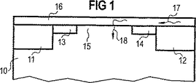
図1に、周知のフォトダイオードの基本構造を示す。シリコン基板10は、弱くドーピングされた、任意の電導性タイプ(例えばp電導性タイプ)の基板である。この基板10では、上述のMOSトランジスターのような電子機能ユニット(図示せず)に対する絶縁のために、トレンチ絶縁11,12が設けられている。これらトレンチ絶縁物11,12は、酸化シリコンを有するいわゆるSTI領域(皿状トレンチ絶縁物)である。トレンチ絶縁物11,12の間の領域には、ゾーン13ならびにゾーン14がある。ゾーン13は、任意の電導性タイプ、つまり、例えばp電導性タイプであり、ゾーン14は、逆の電導性タイプ、つまり、例えばn電導性タイプである。これらのゾーンは、基板10のドーピング濃度と比較して、高いドーピング濃度を有している。基板のドーピングに関する上記した「弱いドーピング」という表現は、つまり、ゾーン13,14のドーピング濃度と比較して低いドーピング濃度であることを意味する。従って、ゾーン13,14の間には、弱くドープされたゾーン15がある。このゾーン15は、実際的に、本質的なゾーン(intrinsische Zone)とも呼ぶことができる。従来のように、低いドーピング濃度をマイナスで、高いドーピング濃度をプラスで示す場合、上記に例としてあげた基板10ならびにゾーン13,14の電導性タイプでは、光電子工学的に活性なダイオード部分は、連続ゾーン、すなわち、p+(ゾーン13)、p−(ゾーン15)、ならびにn+(ゾーン14)を有することとなる。
【0004】
トレンチ絶縁物11,12、およびゾーン13,14,15を有する基板の上に、光波導体16が設けられている。この光波導体16は、例えば窒化シリコン/酸化シリコンから構成される。この光波導体16を流れる、矢印17で図示した光波から、漏波カプラーを介して、光電子工学的に活性なダイオード部分に光が連結される。図1において、光波導体16からゾーン15への光連結を矢印18で示す。なお、当然、ゾーン13,14を経由して連結される光もあるが、特に示していない。連結された光は、ゾーン15で荷電キャリアを生成し、この荷電キャリアが、ゾーン15側でダイオードフォト電流を生成する。
【0005】
上述した形状のフォトダイオードは、ラテラルもしくはプレーナ形ダイオードである。このとき、良い発光量、つまり大きなフォト電流を実現できるよう、光電子工学的に活性なダイオード部分の表面は、側面方向に見られるように、できる限り大きくなければならない。このことは、しかし、集積回路システム中のこのような平坦なフォトダイオードが、大きなチップ面を必要とすることを意味しているため、集積密度を減少させてしまう。大規模集積システムでは、小型構造化への傾向がますます進んでおり、例えば、MOSトランジスターのチャネル長はより一層小さくなっている。このように得られたチップ面も、プレーナ形フォトダイオードを用いることによって、少なくとも部分的には再び無駄となる。この点は、経済的にも特に不利である。なぜなら、チップ面は、大変重要なコスト要因だからである。
【0006】
独国特許公開2624436A1(DE2624436A1)で示されるフォトダイオード構造では、光の連結を改善するため、基板から突き出るメサ形状の構造が用いられている。メサ中の垂直部材に光が連結されるので、結合度は増加する。また、このメサは、エピタキシャル層に形成される。なお、同様のフォトダイオード構造が、独国特許3920219C2(DE3920129C2)に示されている。
【0007】
本発明の目的は、所定の発光量に関して、チップ表面を節約するフォトダイオード構造、特に、より小さなチャネル長を有するトランジスター構造のためのMOS技術に適応されるトランジスター構造を提供することにある。
【0008】
この目的は、請求項1の特徴部分による処置によって解決される。
【0009】
また、上記の構造に関する本発明の基本概念の発展形は、従属請求項に基づいている。
【0010】
以下に、図面に応じた実施形態の説明に基づき、本発明を詳細に説明する。
なお、図1は、上述した周知のフォトダイオードの構造を示す図である。また、図2Aは、垂直フォトダイオードにおける第1実施形態の断面図である。また、図2Bは、図2Aに示した垂直フォトダイオードのレイアウトの一部を示す図である。また、図3は、垂直フォトダイオードにおける第2実施形態の断面図である。また、図4は、垂直電界効果トランジスターの実施形態を示す図であり、これらのようなトランジスターと垂直フォトダイオードとを有する光電子工学的マイクロ電子構造の製造に関する可能性を説明する図である。
【0011】
実施形態の詳細な説明の前に、図面の図は、単に図式的描写であることを指摘する。図面を簡易化するため、例えば、実際の大きさの比率、または、絶縁層またはドープされたゾーンの製造において生じる辺の湾曲などは考慮されていない。
【0012】
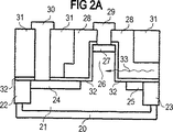
図2Aに示すように、任意の電導性タイプ(好ましくはn電導性タイプ)の領域21が、窪み(Wanne)によってシリコン基板20に形成されている。また、電界効果トランジスターのような更なる機能ユニットが、マイクロ電子構造に設けられている。さらに、この機能ユニットに対する絶縁のため、基板20には、トレンチ絶縁物22,23が、STI領域の形態で設けられている。さらに、基板20におけるトレンチ絶縁物22,23の内側には、ゾーン24,25がある。任意の電導性タイプであるゾーン24,25は、窪み領域21のドーピング濃度に対して高いドーピング濃度を有している。窪み領域21がn電導性タイプであることから考えると、これらのゾーンはn+電導性タイプである。
【0013】
垂直フォトダイオードの構造にとって、メサ26の構造は重要である。メサ26は、基板20から形成され、その上に垂直に立っているため、窪み領域21と同じドーピング濃度で、同じ電導性タイプである。このメサの中で、窪み領域21に面していない側面上に、ゾーン27が設けられている。このゾーン27は、窪み領域とは逆の電導性タイプに設定されており、さらに、比較的に高いドーピング濃度であることが好ましい。窪み領域21がn電導性タイプであることを再び考慮すると、ゾーン27はp+電導性タイプである。
【0014】
これまでに述べた実施形態では、光電子工学的に有効なダイオード部分は、ゾーン24,25(1つの統合されたソーンでもよい)、ゾーン27の下のメサ26のゾーン、ならびにゾーン27によって形成されている。窪み領域21を本質的領域と仮定すると、ピンダイオード構造が考えられる。
【0015】
実施形態の改良形として、p+ゾーン27の替わりに、シリコン層を使用してもよい。このことにより、ショットキーダイオード構造を得られる。
【0016】
どちらの場合にも、ゾーンもしくは層27によって、1つの空乏層(Speerschicht)が形成される。
【0017】
メサ26は、光波導体28によって取り囲まれている。光波導体28は、上記したように、窒化シリコン/酸化シリコンから形成できる。この光波導体28は、基板20の上、好ましくは光学的なコーティング(Verguetung)層32の上で、酸化物(oxid)の上にある。ゾーン27下のメサ26のゾーン領域における光電子工学的に活性なダイオード部分に対する、光波導体28からの光の連結を、矢印33によって示す。
【0018】
フォトダイオード構造は、ゾーン27とゾーン24もしくは25との電気的接触29,30によって完成される。最後に、酸化物および/または窒化物からなる、一点鎖線で示した不活性部(Passivierung)31が設けられる。
【0019】
上記した形状のフォトダイオードにおいて、直立のメサ、従って、垂直に立っている光電子工学的に活性なダイオード部分は、光波導体により取り囲まれていることが発明の要点である。つまり、光波導体は、メサに対しても、光電子工学的に活性なダイオード部分に対しても平行に延びている。これにより、メサの垂直な側壁を経由して、光電子工学的に活性なダイオード部分に光が連結される。このことにより、比較的小さなメサの基本面に、側面の方向に大きな光連結面を形成できる。小さな基本面であるため、図1に示した周知の平坦化構造に対して、より大きい発光量、従ってより大きなフォト電流を得られる。さらに、メサの縦延長方向に対して平行に延びている光波導体によって、光電子工学的に活性なダイオード部分に対する望ましい大きな光結合を、基板を介する望ましくない光連結から分離できる。
【0020】
図2Bに示したレイアウト描写に応じた、光波導体28およびメサ26の閉環状構造では、発光量がさらに高まる。なぜなら、いったん反射された光の部分が、後で吸収されるからである。図2Bにおいて、多数の入射光を意味している矢印33により、この現象を図式的に示す。
【0021】
図3に示した垂直フォトダイオードの実施形態(図2A,2Bにおける同じ部材を、同じ符号で示す)では、図2A,2Bに示した実施形態と同様に、基板20は、窪み領域21、トレンチ絶縁物22,23、およびメサ26を備えている。この実施形態で図2A・2Bと異なる点は、互いに異なる電導性タイプを示す高ドープされた2つのゾーン44,45が設けられており、これらのゾーンが、メサ26の下の窪み領域21からその縁に沿って延びていることである。ここでも、窪み領域21がn電導性タイプであると、例えば、ゾーン44はn+電導性タイプ、ゾーン45はp+電導性タイプである。この実施形態においても、メサ26は、影付きで描写された光波導体47によって、環状に取り囲まれていることが好ましい。この光波導体47から、同様に、メサ26の垂直な側壁を経由して光が連結される。これを矢印52で示す。これにより、図2A,2Bに示した実施形態に基づいて説明した有利な効果が同様に生じる。
【0022】
図3に示したフォトダイオードは、ゾーン44,45ならびに一点鎖線で示された不活性部51のための電気的接触48,49によって完成される。
【0023】
上述の形態にかかる本発明のフォトダイオードは、従来の垂直電界効果トランジスターを有する集積回路に対する集積に好適である。このようなトランジスターを図4に示す。このトランジスターは、同様に窪み領域61を備える基板60の上に形成される。nチャネルトランジスターの場合、この窪み領域61はp電導性タイプである。集積回路の他の機能ユニットに対する絶縁物は、トレンチ絶縁物62,63(STI領域)により形成されている。窪み領域61には、隣接ゾーン64が設けられている。このゾーン64は、窪み領域61の電導性タイプとは逆の電導性タイプを有し、比較的に高いドーピング濃度である。この窪み領域がp電導性タイプであると、ゾーン64はn+電導性タイプである。ゾーン66は、メサ65の、窪み領域61に面していない側面上にある。窪み領域61、ゾーン64、ならびにメサ65が上述した電導性タイプである場合、このゾーン66は、n+電導性タイプである。トランジスターの構造は、スペーサー67,接触68,69および一点鎖線で描写された不活性部70によって完成される。スペーサー67は、メサ基板に対して絶縁されているポリシリコンまたは非結晶シリコンである。また、接触68,69は、ゾーン64,66のためのものである。
【0024】
なお、pチャネルトランジスターを形成するために、窪み領域61、ゾーン64、メサ65およびゾーン66の電導性タイプを、上記と反対にすることもできる。
【0025】
図2A,2B,3および4の比較から明らかな通り、本発明による垂直フォトダイオードの構造は、CMOSプロセスに対する集積に特に適している。例えば、垂直構造のフォトダイオードおよび電界効果トランジスターを有する光電子工学的マイクロ電子構造の集積において、チップ上の光学伝送経路(optischen Uebertragungsstrecken)における受信部としてフォトダイオードを機能させる場合、電気的な接続と端子とに用いるメタライジング層の数を減少できる。さらに、例えば、スペーサー技術などの自己整合技術を使用することにより、リソグラフィーの最小幅より薄いスペーサーを用いることで、集積密度を高められる。
【0026】
また、図4に示したメサ構造を有する垂直電界効果トランジスターの代わりに、環状もしくは板状のトランジスターを垂直フォトダイオードと共に集積する場合、電気的性質を「能動的に」改良できる。特に、寄生バイポーラ効果および短チャネル効果を回避できる。
【0027】
本発明による光電子工学的マイクロ電子構造の集積における個々のプロセス工程は、従来の方法である。従って、特に、トレンチ絶縁物を製造するためのSTI工程において、窪みの埋め込み(Implantationen)、そして、場合によっては図2Aに示したゾーン27を形成するための追加の埋め込みの後に、メサの構造のための窒化物マスクを製造することは特別な意味がある。なぜなら、このメサの高さによって、電界効果トランジスターのチャネル長、ならびにフォトダイオードの透過するべき軌道領域の高さが決定されるからである。フォトダイオードの全面は、このメサの高さと、基板における側面方向の幅とによって決定される。ゲート酸化物、ゲートポリシリコンまたはメタルゲート材料については、従来のように成長もしくは析出させる。このとき、ポリシリコンゲートはマスクによって形成される。このマスクは、図2A,2Bに示したフォトダイオードの側壁を保護するためにも使用できる。電界効果トランジスターのソース/ドレイン領域、ならびにフォトダイオードのドープ領域については、埋め込み技術(Implantationstechniken)によって製造する。図2A,2B,および図3に示した層32,50のような酸化コーティング層は、場合によっては、別々に塗付されることもある。また、適切な屈折率を有する材料からなる光波導体を塗付し、マスクによって構造化する。最後に、不活性物質を塗付し、コンタクトホールのエッチング、シリコン化、およびメタライジングなどのプロセスを行う。なお、ショットキーダイオードの形成のために、図2Aに示したドープされたゾーン27の替わりにシリコン層を使用する場合には、シリコン化を行う。また、光電子工学材料としては、シリコンの他に、化合物半導体を用いることもできる。
【図面の簡単な説明】
【図1】 上述した周知のフォトダイオードの構造を示す図である。
【図2A】 垂直フォトダイオードにおける第1実施形態の断面図である。
【図2B】 図2Aに示した垂直フォトダイオードのレイアウトの一部を示す図である。
【図3】 垂直フォトダイオードにおける第2実施形態の断面図である。
【図4】 垂直電界効果トランジスターの実施形態を示す図であり、これらのようなトランジスターと垂直フォトダイオードとを有する光電子光学的マイクロ電子構造の製造に関する可能性を説明する図である。The present invention relates to a photodiode according to the premise of claim 1 .
[0001]
In microelectronics, in addition to pure electronic structures such as integrated semiconductor circuits in which electronic functional units such as transistors, diodes, and capacitors are integrated on a semiconductor substrate, such electronic functional units are combined with optical elements. Has also become common. Here, the latest semiconductor technology makes it possible to integrate a photosensor in the form of a photodiode and a lightwave conductor having an electronic system such as an amplifier in an integrated structure. Such integration is performed, for example, by MOS technology. In this technology, the production of photosensors and lightwave conductors in the form of photodiodes is compatible with the production of electronic amplifier functional units.
[0002]
A photoelectron optical microelectronic structure of the type described above is basically known from "Microelectronics Technology", 1991,
[0003]
FIG. 1 shows a basic structure of a known photodiode. The
[0004]
A
[0005]
The photodiode having the above-described shape is a lateral or planar diode. At this time, the surface of the optoelectronically active diode portion must be as large as possible so that it can be seen in the lateral direction so that a good light emission amount, that is, a large photocurrent can be realized. This, however, means that such a flat photodiode in an integrated circuit system requires a large chip surface, thus reducing the integration density. In large-scale integrated systems, the trend toward miniaturization is increasing, and for example, the channel length of MOS transistors is becoming even smaller. The chip surface thus obtained is also at least partially wasted again by using a planar photodiode. This point is also particularly disadvantageous economically. This is because the chip surface is a very important cost factor.
[0006]
In the photodiode structure shown in German Offenlegungsschrift 2624436A1 (DE 2624436A1), a mesa-shaped structure protruding from the substrate is used in order to improve light coupling. Since light is coupled to the vertical member in the mesa, the degree of coupling increases. The mesa is formed in the epitaxial layer. A similar photodiode structure is shown in German Patent 3920219C2 (DE3920129C2).
[0007]
It is an object of the present invention to provide a transistor structure adapted for MOS technology for a photodiode structure that saves the chip surface for a given amount of light emission, in particular a transistor structure having a smaller channel length.
[0008]
This object is solved by the measures according to the features of claim 1.
[0009]
The development of the basic concept of the invention with respect to the above structure is also based on the dependent claims.
[0010]
Below, based on description of embodiment according to drawing, this invention is demonstrated in detail.
FIG. 1 is a diagram showing the structure of the known photodiode described above. FIG. 2A is a cross-sectional view of the first embodiment of the vertical photodiode. FIG. 2B is a diagram showing a part of the layout of the vertical photodiode shown in FIG. 2A. FIG. 3 is a cross-sectional view of the second embodiment of the vertical photodiode. FIG. 4 is a diagram illustrating an embodiment of a vertical field effect transistor , illustrating the possibility of manufacturing an optoelectronic microelectronic structure having such a transistor and a vertical photodiode.
[0011]
Before the detailed description of the embodiments, it is pointed out that the figures in the drawings are merely schematic representations. In order to simplify the drawing, for example, the actual size ratio or the edge curvatures that occur in the production of the insulating layer or doped zone are not taken into account.
[0012]
As shown in FIG. 2A, a
[0013]
The structure of the
[0014]
In the embodiments described so far, the optoelectronically effective diode portion is formed by
[0015]
As an improved form of the embodiment, a silicon layer may be used instead of the p + zone 27. As a result, a Schottky diode structure can be obtained.
[0016]
In either case, the zone or
[0017]
The
[0018]
The photodiode structure is completed by
[0019]
In the photodiode of the above-mentioned shape, it is the main point of the invention that the upright mesa, and thus the vertically optoelectronically active diode part, is surrounded by the lightwave conductor. That is, the lightwave conductor extends parallel to the mesa and to the optoelectronically active diode portion. This couples light to the optoelectronically active diode portion via the vertical side walls of the mesa. This makes it possible to form a large optical coupling surface in the direction of the side surface on the relatively small mesa basic surface. Because of the small basic surface, a larger light emission amount and thus a larger photocurrent can be obtained with respect to the well-known planarization structure shown in FIG. In addition, a lightwave conductor extending parallel to the longitudinal direction of the mesa allows the desired large optical coupling to the optoelectronically active diode part to be separated from unwanted optical coupling through the substrate.
[0020]
In the closed annular structure of the
[0021]
In the embodiment of the vertical photodiode shown in FIG. 3 (the same members in FIGS. 2A and 2B are indicated by the same reference numerals), the
[0022]
The photodiode shown in FIG. 3 is completed by
[0023]
The photodiode of the present invention according to the above-described embodiment is suitable for integration on an integrated circuit having a conventional vertical field effect transistor . Such a transistor is shown in FIG. The transistor is formed on a
[0024]
In order to form a p-channel transistor, the conductivity type of the
[0025]
As is clear from a comparison of FIGS. 2A, 2B, 3 and 4, the structure of the vertical photodiode according to the invention is particularly suitable for integration for CMOS processes. For example, in the integration of optoelectronic microelectronic structures with vertical photodiodes and field effect transistors , electrical connections and terminals when the photodiode functions as a receiver in an optical transmission path on the chip (optischen Uebertragungsstrecken) The number of metallizing layers used for the above can be reduced. Furthermore, for example, by using a self-alignment technique such as a spacer technique, the integration density can be increased by using a spacer thinner than the minimum width of lithography.
[0026]
Also, instead of the vertical field effect transistor having the mesa structure shown in FIG. 4, when an annular or plate-like transistor is integrated with a vertical photodiode, the electrical properties can be “actively” improved. In particular, the parasitic bipolar effect and the short channel effect can be avoided.
[0027]
The individual process steps in the integration of optoelectronic microelectronic structures according to the present invention are conventional methods. Thus, in particular in the STI process for manufacturing the trench insulator, after the recess implantation, and possibly after the additional implantation to form the
[Brief description of the drawings]
FIG. 1 is a diagram showing the structure of a known photodiode described above.
FIG. 2A is a cross-sectional view of a first embodiment of a vertical photodiode.
FIG. 2B is a diagram showing a part of the layout of the vertical photodiode shown in FIG. 2A.
FIG. 3 is a cross-sectional view of a second embodiment of a vertical photodiode.
FIG. 4 is a diagram illustrating an embodiment of a vertical field effect transistor , illustrating the possibility of manufacturing an opto-optical microelectronic structure having such a transistor and a vertical photodiode.
Claims (6)
この半導体基板(20)の中に形成され、ドープされた窪み(21)と、
上記半導体基板(20)から立ち上がっているメサ(26)であって、上記窪み(21)と同じ電導性タイプの部分(26)を備えたメサ(26)と、
空乏層を形成するドーピング領域(24,25,26,27;44,45,26)によって構成されており、一部はメサ(26)に、一部は半導体基板(20)に形成された窪み(21)の内側に配置されている光電子工学的に活性な部分と、
上記半導体基板に形成された窪み(21)に配置された集積光波導体(28,47)であって、メサ(26)を取り囲むことで、メサ(26)の側壁および窪み(21)の表面を経由させて、上記光電子工学的に活性なダイオード部分に光を連結させる集積光波導体(28,47)とを含むフォトダイオード。A semiconductor substrate (20);
A doped depression (21) formed in the semiconductor substrate (20);
A mesa (26) rising from the semiconductor substrate (20), comprising a portion (26) of the same conductivity type as the depression (21);
It is constituted by doping regions (24, 25, 26, 27; 44, 45, 26) that form a depletion layer, partly formed in the mesa (26) and partly formed in the semiconductor substrate (20). An optoelectronically active portion located inside (21);
An integrated lightwave conductor (28, 47) disposed in a recess (21) formed in the semiconductor substrate, and surrounding the mesa (26), so that the side wall of the mesa (26) and the surface of the recess (21) are A photodiode comprising an integrated lightwave conductor (28, 47) through which light is coupled to the optoelectronically active diode portion.
上記半導体基板(20)に面していないメサ(26)の端部に配置され、窪み(21)と逆の電導性タイプを生じるドーピングを有するゾーン(27)と、
半導体基板の表面の窪み(21)の内側に配置され、上記窪み(21)と比較して同じ電導性タイプでより高いドーピング剤濃度であるゾーン(24,25)と、
上記メサの部分(26)とを含んでいることを特徴とする請求項1に記載のフォトダイオード。The optoelectronically active diode part above is
A zone (27) with doping arranged at the end of the mesa (26) not facing the semiconductor substrate (20), resulting in a conductivity type opposite to the depression (21);
A zone (24, 25) which is arranged inside a depression (21) on the surface of the semiconductor substrate and which has the same conductivity type and a higher dopant concentration compared to the depression (21);
2. A photodiode according to claim 1, characterized in that it includes a mesa portion (26).
上記窪み(21)と同じ電導性タイプを生じるドーピングを有するとともに、窪み(21)と比較して高いドーピング濃度である第1ゾーン(44)と、
上記窪み(21)と逆の電導性タイプを生じるドーピングを有するとともに、窪み(21)と比較して高いドーピング濃度である第2ゾーン(45)と、
上記メサの部分(26)とを有し、
上記第1および第2ゾーン(44,45)が、上記メサ(26)の側壁、ならびに半導体基板(20)の中に形成された窪み(21)の表面にそれぞれ配置されていることを特徴とする請求項1に記載のフォトダイオード。The optoelectronically active diode part above is
A first zone (44) having a doping that produces the same conductivity type as the depression (21) and having a higher doping concentration compared to the depression (21);
A second zone (45) having a doping that produces a conductivity type opposite to the depression (21) and having a higher doping concentration compared to the depression (21);
The mesa part (26),
The first and second zones (44, 45) are respectively disposed on the side wall of the mesa (26) and the surface of a recess (21) formed in the semiconductor substrate (20). The photodiode according to claim 1.
Applications Claiming Priority (2)
| Application Number | Priority Date | Filing Date | Title |
|---|---|---|---|
| DE19942692A DE19942692B4 (en) | 1999-09-07 | 1999-09-07 | Optoelectronic microelectronic assembly |
| PCT/DE2000/003073 WO2001018867A1 (en) | 1999-09-07 | 2000-09-06 | Optoelectronic-microelectronic assembly |
Publications (3)
| Publication Number | Publication Date |
|---|---|
| JP2004500704A JP2004500704A (en) | 2004-01-08 |
| JP2004500704A5 JP2004500704A5 (en) | 2004-12-24 |
| JP3836026B2 true JP3836026B2 (en) | 2006-10-18 |
Family
ID=7921097
Family Applications (1)
| Application Number | Title | Priority Date | Filing Date |
|---|---|---|---|
| JP2001522591A Expired - Fee Related JP3836026B2 (en) | 1999-09-07 | 2000-09-06 | Photodiode |
Country Status (5)
| Country | Link |
|---|---|
| US (1) | US6553157B2 (en) |
| JP (1) | JP3836026B2 (en) |
| KR (1) | KR100443685B1 (en) |
| DE (1) | DE19942692B4 (en) |
| WO (1) | WO2001018867A1 (en) |
Families Citing this family (8)
| Publication number | Priority date | Publication date | Assignee | Title |
|---|---|---|---|---|
| CA2365499C (en) | 2000-12-26 | 2011-02-15 | National Research Council Of Canada | High speed and high efficiency si-based photodetectors using waveguides formed with silicides for near ir applications |
| DE10123363A1 (en) * | 2001-05-14 | 2002-11-28 | Infineon Technologies Ag | Structure for integrated circuit arranged above substrate has elements separated by distance greater than/equal to resolution of lithographic technique used to structure at least parts of structure |
| US7010208B1 (en) * | 2002-06-24 | 2006-03-07 | Luxtera, Inc. | CMOS process silicon waveguides |
| JP4227513B2 (en) * | 2003-12-26 | 2009-02-18 | 浜松ホトニクス株式会社 | Semiconductor photo detector |
| US8682116B2 (en) | 2007-08-08 | 2014-03-25 | Infineon Technologies Ag | Integrated circuit including non-planar structure and waveguide |
| KR101419802B1 (en) * | 2010-09-09 | 2014-07-17 | 한국전자통신연구원 | Electro-optic device and mach-zehnder optical modulator used the same |
| US10666353B1 (en) * | 2018-11-20 | 2020-05-26 | Juniper Networks, Inc. | Normal incidence photodetector with self-test functionality |
| US10739622B2 (en) * | 2018-12-28 | 2020-08-11 | Juniper Networks, Inc. | Integrated optoelectronic device with heater |
Family Cites Families (7)
| Publication number | Priority date | Publication date | Assignee | Title |
|---|---|---|---|---|
| DE2624436C2 (en) * | 1976-06-01 | 1982-11-04 | Licentia Patent-Verwaltungs-Gmbh, 6000 Frankfurt | Optical fiber with integrated detector element |
| US4744623A (en) * | 1985-10-16 | 1988-05-17 | The Trustees Of Columbia University In The City Of New York | Integrated fiber optic coupler for VHSIC/VLSI interconnects |
| DE3920219A1 (en) * | 1989-06-21 | 1991-01-10 | Licentia Gmbh | Operating optical detector with active semiconductor detector layer - impinging radiation to be detected on side face under Brewster angle |
| US4970386A (en) * | 1989-06-22 | 1990-11-13 | Westinghouse Electric Corp. | Vertical FET high speed optical sensor |
| JP2910696B2 (en) * | 1996-09-20 | 1999-06-23 | 日本電気株式会社 | Semiconductor photodetector |
| US6387720B1 (en) * | 1999-12-14 | 2002-05-14 | Phillips Electronics North America Corporation | Waveguide structures integrated with standard CMOS circuitry and methods for making the same |
| US6392257B1 (en) * | 2000-02-10 | 2002-05-21 | Motorola Inc. | Semiconductor structure, semiconductor device, communicating device, integrated circuit, and process for fabricating the same |
-
1999
- 1999-09-07 DE DE19942692A patent/DE19942692B4/en not_active Expired - Fee Related
-
2000
- 2000-09-06 WO PCT/DE2000/003073 patent/WO2001018867A1/en active IP Right Grant
- 2000-09-06 JP JP2001522591A patent/JP3836026B2/en not_active Expired - Fee Related
- 2000-09-06 KR KR10-2002-7003057A patent/KR100443685B1/en not_active IP Right Cessation
-
2002
- 2002-03-07 US US10/093,320 patent/US6553157B2/en not_active Expired - Lifetime
Also Published As
| Publication number | Publication date |
|---|---|
| JP2004500704A (en) | 2004-01-08 |
| KR100443685B1 (en) | 2004-08-09 |
| DE19942692B4 (en) | 2007-04-12 |
| KR20020030105A (en) | 2002-04-22 |
| US20020110329A1 (en) | 2002-08-15 |
| US6553157B2 (en) | 2003-04-22 |
| DE19942692A1 (en) | 2001-04-12 |
| WO2001018867A1 (en) | 2001-03-15 |
Similar Documents
| Publication | Publication Date | Title |
|---|---|---|
| US4737472A (en) | Process for the simultaneous production of self-aligned bipolar transistors and complementary MOS transistors on a common silicon substrate | |
| US6323525B1 (en) | MISFET semiconductor device having relative impurity concentration levels between layers | |
| KR20040008912A (en) | Hybrid isolation method for Image sensor | |
| US6956255B2 (en) | Semiconductor device and drive circuit using the semiconductor devices | |
| US5488251A (en) | Semiconductor device and process for producing the same | |
| KR20020034870A (en) | Integrated circuits with reduced substrate capacitance | |
| JP3836026B2 (en) | Photodiode | |
| EP1191583A2 (en) | Low voltage transistor | |
| KR970011641B1 (en) | Semiconductor device and method of manufacturing the same | |
| US20070254398A1 (en) | Method of manufacturing semiconductor device | |
| KR100674142B1 (en) | SON MOSFET using beam structure and inverter using thereof and the method of fabricating thereof | |
| US6429056B1 (en) | Dynamic threshold voltage devices with low gate to substrate resistance | |
| JPH10335484A (en) | Manufacture of semiconductor device | |
| US5717227A (en) | Bipolar junction transistors having insulated gate electrodes | |
| US20020009842A1 (en) | High-voltage device and method for manufacturing high-voltage device | |
| WO2022215360A1 (en) | Solid-state imaging element, and method for manufacturing solid-state imaging element | |
| JP3247106B2 (en) | Manufacturing method and structure of integrated circuit | |
| KR100520466B1 (en) | Image sensor and manufacturing method | |
| JP2003224252A (en) | Optical semiconductor integrated circuit device | |
| JPS61258471A (en) | Semiconductor integrated circuit device | |
| KR100273687B1 (en) | Bipolar transistor and method for forming the same | |
| JPH11307544A (en) | Bipolar transistor and semiconductor integrated circuit device | |
| US20040084723A1 (en) | Semiconductor device having complementary mos transistor | |
| KR100381015B1 (en) | Method for fabricating semiconductor device | |
| KR0128022B1 (en) | Fabrication method of homojunction bipolar transistor device with silicon-on-insulator substrate |
Legal Events
| Date | Code | Title | Description |
|---|---|---|---|
| A131 | Notification of reasons for refusal |
Free format text: JAPANESE INTERMEDIATE CODE: A131 Effective date: 20051220 |
|
| A521 | Request for written amendment filed |
Free format text: JAPANESE INTERMEDIATE CODE: A523 Effective date: 20060316 |
|
| RD02 | Notification of acceptance of power of attorney |
Free format text: JAPANESE INTERMEDIATE CODE: A7422 Effective date: 20060316 |
|
| TRDD | Decision of grant or rejection written | ||
| A01 | Written decision to grant a patent or to grant a registration (utility model) |
Free format text: JAPANESE INTERMEDIATE CODE: A01 Effective date: 20060627 |
|
| A61 | First payment of annual fees (during grant procedure) |
Free format text: JAPANESE INTERMEDIATE CODE: A61 Effective date: 20060725 |
|
| R150 | Certificate of patent or registration of utility model |
Free format text: JAPANESE INTERMEDIATE CODE: R150 |
|
| FPAY | Renewal fee payment (event date is renewal date of database) |
Free format text: PAYMENT UNTIL: 20090804 Year of fee payment: 3 |
|
| FPAY | Renewal fee payment (event date is renewal date of database) |
Free format text: PAYMENT UNTIL: 20100804 Year of fee payment: 4 |
|
| FPAY | Renewal fee payment (event date is renewal date of database) |
Free format text: PAYMENT UNTIL: 20110804 Year of fee payment: 5 |
|
| FPAY | Renewal fee payment (event date is renewal date of database) |
Free format text: PAYMENT UNTIL: 20110804 Year of fee payment: 5 |
|
| FPAY | Renewal fee payment (event date is renewal date of database) |
Free format text: PAYMENT UNTIL: 20120804 Year of fee payment: 6 |
|
| FPAY | Renewal fee payment (event date is renewal date of database) |
Free format text: PAYMENT UNTIL: 20120804 Year of fee payment: 6 |
|
| FPAY | Renewal fee payment (event date is renewal date of database) |
Free format text: PAYMENT UNTIL: 20130804 Year of fee payment: 7 |
|
| R250 | Receipt of annual fees |
Free format text: JAPANESE INTERMEDIATE CODE: R250 |
|
| R250 | Receipt of annual fees |
Free format text: JAPANESE INTERMEDIATE CODE: R250 |
|
| R250 | Receipt of annual fees |
Free format text: JAPANESE INTERMEDIATE CODE: R250 |
|
| R250 | Receipt of annual fees |
Free format text: JAPANESE INTERMEDIATE CODE: R250 |
|
| LAPS | Cancellation because of no payment of annual fees |