JP3829669B2 - Electro-optical device and electronic apparatus - Google Patents
Electro-optical device and electronic apparatus Download PDFInfo
- Publication number
- JP3829669B2 JP3829669B2 JP2001261578A JP2001261578A JP3829669B2 JP 3829669 B2 JP3829669 B2 JP 3829669B2 JP 2001261578 A JP2001261578 A JP 2001261578A JP 2001261578 A JP2001261578 A JP 2001261578A JP 3829669 B2 JP3829669 B2 JP 3829669B2
- Authority
- JP
- Japan
- Prior art keywords
- region
- electro
- angle
- connection
- optical device
- Prior art date
- Legal status (The legal status is an assumption and is not a legal conclusion. Google has not performed a legal analysis and makes no representation as to the accuracy of the status listed.)
- Expired - Lifetime
Links
Images


Description
【0001】
【発明の属する技術分野】
本発明は、シール材の内側に形成された表示領域とシール材の外側に形成された接続端子とを複数の接続線により接続して成る電気光学装置及びそれを用いる電子機器に関する。
【0002】
【従来の技術】
一対の基板間に液晶を封入した液晶装置では、表示領域の周囲に配置されたシール材により一対の基板を重ね合わせて接合している。一対の基板間のシール材の内側の領域には液晶が封入される。マトリクスタイプの液晶装置では、表示領域に平行に配置された複数の表示ラインのそれぞれに、基板上に形成された接続線の一端が接続され、その接続線がシール材の外側まで引き出される。接続線の他端には接続端子が形成され、いわゆるCOG(Chip On Glass)タイプの液晶装置ではその接続端子に液晶パネル駆動用ICの出力端子、すなわちバンプが接続される。
【0003】
一般に、液晶パネル駆動用ICのバンプの間隔と、表示領域の表示ラインの間隔は同一でないため、それらバンプとそれら表示ラインとをつなぐ接続線の間隔は、バンプから表示ラインに向けて、あるいはその逆の方向に向けて、広がるような形状に形成される。
【0004】
なお、本明細書で、「間隔」とは、互いに隣り合う物体間のピッチをいう。また、「間隙幅」とは、互いに隣り合う物体の間に形成される間隙の幅をいう。
【0005】
【発明が解決しようとする課題】
通常、液晶パネル駆動用ICのバンプの間隔は表示領域の幅に関わりなく定められている。このため、表示領域の幅又は面積が大きく設定されている場合には、表示領域を構成する表示ラインの間隔と、液晶パネル駆動用ICのバンプの間隔との差が著しく拡大する。特に、液晶パネル駆動用ICのバンプの間隔が狭い仕様のものを用いる場合には、さらにこの間隔の差が顕著となる。
【0006】
これらの間隔の差は、接続線の間隔が所定の方向に向けて広がるように接続線を斜めに形成することにより無くすことができるが、接続線の傾斜角度には限界がある。すなわち、傾斜角度を大きくし過ぎれば、接続線の間隔が狭まることにより、特に隣り合った接続線間の間隙幅が狭まり、このため、コロージョン等といった不良発生のおそれがある。つまり、接続線の傾斜角度を大きくすることには限度がある。
【0007】
また、接続線の傾斜角度を小さくすれば上記のようなコロージョンの問題は解消するが、この場合には、傾斜角度を小さくするほど表示領域と液晶パネル駆動用ICとの間の距離が大きくなって表示領域の周囲に必要な実装スペースが拡大し、表示領域に対して液晶装置が大型になってしまうという問題がある。
【0008】
本発明は、上記の問題点に鑑みて成されたものであって、コロージョン等といった不良の発生を抑制しつつ、小型化を達成できる電気光学装置及び電子機器を提供することを目的とする。
【0009】
【課題を解決するための手段】
(1) 上記の目的を達成するため、本発明に係る電気光学装置は、互いに重ね合される第1の基板及び第2の基板と、前記第1の基板及び前記第2の基板を表示領域の周囲で接合するシール材と、前記第2の基板から張り出して形成された前記第1の基板の張出し部に設けられた複数の接続端子と、前記第1の基板上に設けられ、前記表示領域と前記複数の接続端子とを接続する複数の接続線とを備え、前記シール材の内側における前記接続線の間隔が、前記シール材の外側における前記接続線の間隔よりも小さいことを特徴とする。
【0010】
この電気光学装置によれば、シール材の内側における接続線の間隔が、シール材の外側における接続線の間隔よりも小さいので、コロージョン等といった不良が発生するおそれのあるシール材の外側の領域では、接続線の間隔を大きくでき、結果的に接続線の間隙幅を大きくすることができ、これにより、コロージョン等の発生を防止できる。
【0011】
他方、コロージョン等といった不良が発生するおそれのないシール材の内側の領域では、接続線の間隔を小さくすることができ、このように接続線の間隔を小さくすれば、表示領域と接続端子との間の距離を小さくすることができる。そしてこれにより、電気光学装置の平面的な外形形状を小さくすることができる。
【0012】
つまり、上記構成の電気光学装置によれば、コロージョン等といった不良の発生を抑制しつつ、電気光学装置の平面的な外形形状を小型にすることができる。なお、上記構成において、シール材の内側の領域では、接続線の間隔を製造上可能な限りに小さくすること、例えばパターニング工程におけるレジストの解像度で決まる間隔に設定することができる。また、シール材の外側の領域では、コロージョン等といった不良の発生を防止できる程度の接続線間の間隙幅を確保できるように、接続線の間隔を決定することができる。
【0013】
また、上記構成において、接続端子には、電気光学パネル駆動用ICのバンプが接続されても良いし、あるいは、フレキシブルプリント基板に形成された端子が接続されても良い。フレキシブルプリント基板に形成された端子が接続される場合には、接続端子を介して電気光学装置が外部回路と接続される。
【0014】
上記構成の電気光学装置は、具体的には、液晶装置、プラズマディスプレイ装置、エレクトロルミネッセンス表示装置等といった各種の電気光学装置に広く適用できる。
【0015】
(2) 次に、本発明に係る他の電気光学装置は、互いに重ね合される第1の基板及び第2の基板と、前記第1の基板及び前記第2の基板を表示領域の周囲で接合するシール材と、前記第2の基板から張り出して形成された前記第1の基板の張出し部に設けられた複数の接続端子と、前記第1の基板上に設けられ、前記表示領域に形成された複数の表示ラインの各々と前記複数の接続端子の各々とを接続する複数の接続線とを備え、前記シール材の内側における前記接続線の間隔が、前記シール材の外側における前記接続線の間隔よりも小さいことを特徴とする。
【0016】
この構成の電気光学装置は、上記(1)項に記載した構成の電気光学装置に対して、「表示領域に複数の表示ラインが形成され、その表示ラインに接続線が接続される」ことにおいて違いがある。
【0017】
この電気光学装置によれば、シール材の内側における接続線の間隔が、シール材の外側における接続線の間隔よりも小さいので、コロージョン等といった不良が発生するおそれのあるシール材の外側の領域では、接続線の間隔を大きくでき、結果的に接続線の間隙幅を大きくすることができ、これにより、コロージョン等の発生を防止できる。
【0018】
他方、コロージョン等といった不良が発生するおそれのないシール材の内側の領域では、接続線の間隔を小さくすることができ、このように接続線の間隔を小さくすれば、表示領域と接続端子との間の距離を小さくすることができる。そしてこれにより、電気光学装置の平面的な外形形状を小さくすることができる。
【0019】
つまり、上記構成の電気光学装置によれば、コロージョン等といった不良の発生を抑制しつつ、電気光学装置の平面的な外形形状を小型にすることができる。なお、上記構成において、シール材の内側の領域では、接続線の間隔を製造上可能な限りに小さくすること、例えばパターニング工程におけるレジストの解像度で決まる間隔に設定することができる。また、シール材の外側の領域では、コロージョン等といった不良の発生を防止できる程度の接続線間の間隙幅を確保できるように、接続線の間隔を決定することができる。
【0020】
また、上記構成において、接続端子には、電気光学パネル駆動用ICのバンプが接続されても良いし、あるいは、フレキシブルプリント基板に形成された端子が接続されても良い。フレキシブルプリント基板に形成された端子が接続される場合には、接続端子を介して電気光学装置が外部回路と接続される。
【0021】
上記構成の電気光学装置は、具体的には、液晶装置、プラズマディスプレイ装置、エレクトロルミネッセンス表示装置等といった各種の電気光学装置に広く適用できる。
【0022】
(3) 次に、本発明に係る他の電気機械装置は、上記(2)項に記載した構成の電気光学装置において、前記シール材の内側における前記接続線の前記表示ラインに対する傾斜角度が、前記シール材の外側における前記接続線の前記表示ラインに対する傾斜角度よりも大きいことを特徴とする。
【0023】
この場合には、シール材の内側では、表示ラインの延設方向に関する接続線の長さを抑えつつ、接続線の間隔を大幅に変換することができる。また、シール材の外側では接続線の間隔を拡大できる。
【0024】
(4) 次に、本発明に係る他の電気光学装置は、上記(2)項又は上記(3)項に記載した構成の電気光学装置において、前記接続端子の間隔が、前記表示ラインの間隔よりも小さいことを特徴とする
(5) 次に、本発明に係る他の電気光学装置は、上記(1)項から上記(4)項に記載した構成の電気光学装置において、前記接続端子には電気光学パネル駆動用ICの出力端子が接続されることを特徴とする。この場合、接続端子の間隔は電気光学パネル駆動用ICの出力端子の間隔と同一とされる。なお、電気光学パネルとしては、液晶パネル、有機ELパネル等が考えられる。
【0025】
(6) 次に、本発明に係る他の電気光学装置は、上記(1)項から上記(5)項に記載した構成の電気光学装置において、前記シール材の外側における前記接続線間の間隙幅が、前記シール材の内側における前記接続線間の間隙幅よりも大きいことを特徴とする。この場合には、シール材の外側における接続線間の間隙幅を拡大することにより、コロージョン等といった不良の発生を効果的に防止できる。
【0026】
(7) 次に、本発明に係る電子機器は、電気光学装置と、該電気光学装置を収容する筐体と、前記電気光学装置の動作を制御する制御手段とを有する電子機器において、前記電気光学装置は上記(1)項から上記(6)項に記載した構成の電気光学装置によって構成されることを特徴とする。このような電子機器としては、例えば、携帯電話機、携帯情報端末機等が考えられる。
【0027】
(8) 次に、本発明に係る他の電気光学装置は、互いに重ね合される第1の基板及び第2の基板と、前記第1の基板及び前記第2の基板を表示領域の周囲で接合するシール材と、該シール材の中に混入された導通材と、前記第2の基板から張り出して形成された前記第1の基板の張出し部に設けられた複数の接続端子と、前記第1の基板上に設けられ、前記複数の接続端子に接続し、前記シール材を通過して延びる複数の接続線とを備え、前記シール材の内側における前記接続線の間隔が、前記シール材の外側における前記接続線の間隔よりも小さく、さらに前記シール材を通過する前記接続線の間隔が、前記シール材の内側における前記接続線の間隔よりも大きいことを特徴とする。
【0028】
この電気光学装置によれば、シール材中に存在する導通材により、第1の基板上に形成された導電性のパターンと第2の基板上に形成された導電性のパターンとをその導通材によって導電接続することができる。
【0029】
また、この電気光学装置によれば、シール材を通過する部分の接続線の間隔を大きくしたので、シール材を通過する部分の接続線の隣り合うもの同士が、シール材中に含まれる導通材によってショート、すなわち短絡してしまうことを防止できる。
【0030】
(9) 次に、本発明に係る他の電気光学装置は、基板と、前記基板に支持され、少なくとも表示領域に配置された電気光学層と、前記電気光学層の周囲に設けられたシール材と、前記基板の端部に設けられた複数の接続端子と、前記基板に設けられ、前記表示領域と前記複数の接続端子とを接続する複数の接続線とを備え、前記複数の接続線は、前記シール材の内側における前記接続線の間隔が、前記シール材の外側における前記接続線の間隔よりも小さくなるように、前記シール材の外周よりも内側において、屈曲していることを特徴とする。
【0031】
(10) 次に、本発明に係る他の電気光学装置は、基板と、前記基板に支持され、少なくとも表示領域に配置された電気光学層と、前記電気光学層の周囲に設けられたシール材と、前記基板の端部に設けられ、所定の方向に沿って配列された複数の接続端子と、前記基板に設けられ、前記表示領域に形成された複数の表示ラインの各々と前記複数の接続端子の各々とを接続する複数の接続線とを備え、前記複数の接続線の各々は、第1領域と第2領域とを有しており、前記第1領域は、少なくともその一部が前記シール材の外側に位置するとともに、前記所定の方向に対する小さい方の角度として第1の角度を成しており、前記第2領域は、前記シール材の内側に位置するとともに、前記所定の方向に対する小さい方の角度として第2の角度を成しており、前記第2の角度が前記第1の角度よりも小さく、前記第2領域における前記接続線の間隔が、前記第1領域における前記接続線の間隔よりも小さいことを特徴とする。
【0032】
(11) 次に、本発明に係る他の電気光学装置は、基板と、前記基板に支持され、少なくとも表示領域に配置された電気光学層と、前記電気光学層の周囲に設けられたシール材と、前記基板の端部に設けられ、所定の方向に沿って配列された複数の接続端子と、前記基板に設けられ、前記複数の接続端子に接続される複数の接続線とを備え、前記複数の接続線の各々は、第1領域、第2領域及び第3領域を有しており、前記第1領域は、少なくともその一部が前記シール材の外側に位置するとともに、前記所定の方向に対する小さい方の角度として第1の角度を成しており、前記第2領域は、前記シール材の内側に位置するとともに、前記所定の方向に対する小さい方の角度として第2の角度を成しており、前記第3領域は、前記第1領域及び前記第2領域に接続されるとともに、前記所定の方向に対する小さい方の角度として第3の角度を成しており、前記第3の角度は、前記第1の角度および前記第2の角度よりも大きく、前記第1の角度および前記第2の角度は互いに異なっており、前記第2領域における前記接続線の間隔が、前記第1領域における前記接続線の間隔よりも小さいことを特徴とする。
【0033】
(12) 次に、本発明に係る他の電気光学装置は、上記(11)項に記載した構成の電気光学装置において、前記複数の接続線の各々は、第4領域を更に有し、前記第4領域は、前記第1領域及び前記接続端子に接続されるとともに、前記所定の方向に対して略直交していることを特徴とする。
【0034】
この構成の電気光学装置では、図14(a)に示すように、接続線60の第4領域A4が接続端子61の配列方向Yに対して略直角方向に延びることになる。これに対し、上記の第4領域を設けない場合には、図14(b)に示すように、接続線60が接続端子61の配列方向Yに対して斜めに延びることになる。
【0035】
接続線60を駆動用IC68に接続することを考えれば、接続端子61は駆動用IC68のバンプ69に接触する。ここで、駆動用IC68の貼り付け位置が接続端子61の配列方向Yに対して直角方向にずれる場合を考えると、バンプ69もそれに応じて、図14(a)及び図14(b)に矢印Cで示すように接続端子61の配列方向Yに対して直角方向へ位置ずれする。
【0036】
このとき、図14(b)のように接続線60が斜めにレイアウトされていると、矢印Cのように位置ずれしたバンプ69は容易に接続線60の端子61を外れてしまう。つまり、駆動用IC68の貼り付け位置の位置ずれに対するマージンを大きくとれない。これに対し、図14(a)に示すように、接続端子61の配列方向Yに対して直角方向へ延びる第4領域A4を設けることにすれば、バンプ69が矢印C方向へ位置ずれしたとしてもそのバンプ69は容易には接続線60から外れない。つまり、駆動用IC68の貼り付け位置の位置ずれに対するマージンを大きくとることができる。
【0037】
(13) 次に、本発明に係る他の電気光学装置は、上記(12)項に記載した構成の電気光学装置において、前記第3の角度は略90°であることを特徴とする。
【0038】
(14) 次に、本発明に係る他の電気光学装置は、上記(11)項に記載した構成の電気光学装置において、前記第2の角度は、前記第1の角度よりも小さいことを特徴とする。
【0039】
(15) 次に、本発明に係る他の電気光学装置は、上記(11)項に記載した構成の電気光学装置において、前記複数の接続線のうち、互いに隣り合う2つの前記接続線は、前記第1、第2及び第3領域において、互いに略平行に配置されていることを特徴とする。
【0040】
(16) 次に、本発明に係る他の電気光学装置は、基板と、前記基板に支持され、少なくとも表示領域に配置された電気光学層と、前記電気光学層の周囲に設けられたシール材と、前記基板の端部に設けられた複数の接続端子と、前記基板に設けられ、前記表示領域に形成された複数の表示ラインの各々と前記複数の接続端子の各々とを接続する複数の接続線とを備え、前記複数の接続線の各々は、第1領域と第2領域とを有しており、前記第1領域は、少なくともその一部が前記シール材の外側に位置するとともに、前記表示ラインに対する小さい方の角度として第1の角度を成しており、前記第2領域は、前記シール材の内側に位置するとともに、前記表示ラインに対する小さい方の角度として第2の角度を成しており、前記複数の接続線の各々は、前記第2の角度が前記第1の角度よりも大きくなるように、前記第1領域と前記第2領域との境界において屈曲していることを特徴とする。
【0041】
【発明の実施の形態】
(電気光学装置の第1実施形態)
以下、本発明に係る電気光学装置をアクティブマトリクスタイプの液晶装置に適用した場合の一実施形態について説明する。
【0042】
図1は、電気光学装置の一例である液晶装置を分解して示す斜視図であり、図2はその液晶装置の断面図であり、図3はその液晶装置の等価回路図である。また、図4はその液晶装置の表示領域を構成する複数の画素のうちの1つの構造を示し、特に、(a)はその画素の平面図を示し、(b)は(a)のB−B線に従った断面図を示している。
【0043】
図1及び図2に示すように、液晶装置1は、電気光学パネルとしての液晶パネル2と、液晶パネル2に接続された2つのFPC(Flexible Printed Circuit:フレキシブルプリント基板)3a及び3bと、液晶パネル2の表示面側(すなわち、図1の下面側)に取り付けられた導光体4と、導光体4の液晶パネル2の反対側に設けられた制御基板5とを備える。導光体4の端部側にはバックライトの光源としてのLED21が設けられる。
【0044】
液晶パネル2は、環状のシール材6によって互いに貼り合わされた一対の基板7a及び7bを有する。第1の基板7aのうち第2の基板7bから張り出す部分の表面には、ACF(Anisotropic Conductive Film:異方性導電膜)9aによって電気光学パネル駆動用ICとしての液晶パネル駆動用IC8aが実装される。また、第2の基板7bのうち第1の基板7aから張り出す部分の表面(すなわち、図1の下側表面)には、ACF9bによって電気光学パネル駆動用ICとしての液晶パネル駆動用IC8bが実装される。このように、本実施形態の液晶装置1は、いわゆるCOG(Chip On Glass)タイプの液晶装置として構成されている。
【0045】
図1において、FPC3aには端子31が設けられ、この端子31は液晶パネル2に形成された端子13aに接続される。また、FPC3bには端子32が設けられ、この端子32は液晶パネル2に形成された端子13bに接続される。また、制御基板5には端子34が設けられ、この端子34はFPC3aに形成された端子33に接続される。
【0046】
図2に示すように、第1の基板7aの内面には、矢印A方向から見てドットマトリクス状に配列された複数の画素電極66が形成され、第1の基板7aの外面には偏光板12aが貼り付けられる。また、第2の基板7bの内面には、矢印A方向から見てストライプ状に形成された複数のデータ線52が形成され、第2の基板7bの外面には偏光板12bが貼り付けられる。そして、第1の基板7a、第2の基板7b及びシール材6によって囲まれる間隙、いわゆるセルギャップ内に液晶Lが封入される。
【0047】
第1の基板7a及び第2の基板7bには、必要に応じて各種の光学要素が設けられる。例えば、液晶Lの配向を揃えるための配向膜が各基板の内面に設けられる。また、カラー表示を行う場合には、第1の基板7aに形成された画素電極に対向する部分の第2の基板7bに、R(レッド)、G(グリーン)、B(ブルー)の各色にカラーフィルタが所定の配列で形成され、画素電極に対向しない領域にはブラックマトリクスが形成される。通常、カラーフィルタ及びブラックマトリクスの表面の平滑化及び保護のために平滑化層がコーティングされる。この場合、第2の基板7b側に設けられる対向電極は平滑層の上に形成される。
【0048】
図3に示すように、液晶パネル2には複数の走査線51が行方向(すなわち、X方向)に形成され、さらに、複数のデータ線52が列方向(すなわち、Y方向)に形成される。走査線51とデータ線52との各交差点に画素53が形成される。各画素53は、液晶層54とTFD(Thin Film Diode)素子56との直列接続によって形成される。各走査線51は液晶パネル駆動用IC8aによって駆動され、各データ線52は液晶パネル駆動用IC8bによって駆動される。
【0049】
走査線51及びTFD素子56は図1及び図2に示す第1の基板7aの内面に形成され、第1の基板7aの内面に形成される画素電極66は走査線51につながる。一方、データ線52は第2の基板7bの内面にストライプ状の電極として形成される。第1の基板7aと第2の基板7bは、1列分の画素電極66と1本のデータ線52とが互いに対向する位置関係となるように、互いに貼り合わされる。このため、液晶層54は、データ線52と画素電極66とこれらの間に挟まれる液晶Lによって構成されることになる。
【0050】
データ線52及び画素電極66は、例えば、ITO(Indium Tin Oxide)等といった透明導電材によって形成される。但し、画素電極66はAl(アルミニウム)等といった光反射性材料によって形成することもできる。なお、図3ではTFD素子56が走査線51の側に接続され、液晶層54がデータ線52の側に接続されているが、これとは逆に、TFD素子56をデータ線の側に接続し、液晶層54を走査線51の側に接続することもできる。
【0051】
液晶装置1は、図4に示すように、いわゆるバック・ツー・バック(Back-to-Back)構造と呼ばれるMIM素子46を備える。このMIM素子46は、一対のMIM素子要素46a及び46bを電気的に逆向きに直列接続することによって形成される。このバック・ツー・バック構造により、1個のMIM素子要素を用いる場合に比べて安定したスイッチング特性を得ることができる。
【0052】
個々のMIM素子要素46a,46bは、第1金属層42/絶縁層43/第2金属層44から成る層構造によって形成される。第1金属層42は例えばTa(タンタル)によって形成され、絶縁層43は例えばTa2O5によって形成され、第2の金属層44は例えばCr(クロム)によって形成される。今、MIM素子46が液晶パネルのアクティブ素子として用いられる場合を考えると、一方のMIM素子要素46aの第2の金属層44が走査電極又は信号電極として作用する信号線、本実施形態では走査線51につながり、他方のMIM素子要素46bの第2の金属層44が画素電極66につながる。
【0053】
図5に示すように、各走査線51にはそれぞれ接続線70の一端が接続される。複数の接続線70のそれぞれの他端には接続端子71が形成され、これらの接続端子71は配列方向Yに沿って配列されている。これらの接続端子71には、液晶パネル駆動用IC8a(図2参照)の出力端子であるバンプ81がそれぞれACF9aを介して接続される。こうして、液晶パネル駆動用IC8aの出力端子は接続線70を介して走査線51に接続される。
【0054】
図5は接続線70の形状を概念的に示している。各接続線70は、少なくともその一部がシール材6の外側に位置する第1領域A1を有する。この第1領域A1は、接続端子71に近い側で配列方向Yと平行に延びる境界線L0と、シール材6の内部において配列方向Yと平行に延びる境界線L1との間にある領域である。また、各接続線70は、シール材6の内側に位置する第2領域A2を有する。この第2領域A2は、前記境界線L1と走査線51の先端との間にある領域である。なお、複数の接続線70は、第1領域A1及び第2領域A2の個々の領域内においては互いに平行に配置されている。
【0055】
各接続線70の第1領域A1は、接続端子71の配列方向Yに対して小さい方の角度として第1角度β1を成している。また、第2領域A2は、配列方向Yに対して小さい方の角度として第2角度β2を成している。そして、本実施形態の場合、
β1>β2
に設定されている。
【0056】
また、図5において、接続線70は、シール材6が設けられた領域を境界として、走査線51に近接した領域である第2領域A2において走査線51の延在方向に対して小さい方の角度α2で傾斜する方向に引き延ばされており、これに対して端子71に近接した第1領域A1では走査線51の延在方向に対して、小さい方の角度α1で傾斜する方向に引き延ばされており、そして
α2>α1
に設定されている。
【0057】
接続線70に関する角度を以上のように設定することにより、複数の接続線70の第2領域A2同士の間隔は、第1領域A1同士の間隔よりも小さくなっている。つまり、接続線70の間隔は、シール材6の内側に形成されていて走査線51に近接した第2領域A2で小さく、他方、シール材6の外側に形成されていて端子71に近接した第1領域A1で、より大きくされている。
【0058】
一般に、シール材の外側においては、コロージョン等といった不良が発生するおそれがあるが、上記のように、接続線70の間隔をシール材6の外側で大きく設定すれば、シール材6の外側においてコロージョン等といった不良の発生を防止することができる。また、コロージョン等の発生のおそれがないシール材6の内側では、パターニング工程におけるレジストの解像度等で決まる製造上の限界近くまで接続線70の間隔を小さく、且つ接続線70の角度を急峻にすることで、液晶パネル2の小型化を達成できる。
【0059】
図6は接続線の変形例を示している。この変形例において、各接続線70は、少なくともその一部がシール材6の外側に位置する第1領域A1を有する。この第1領域A1は、境界線L2と、境界線L3と、接続端子71の列とによって囲まれる領域である。また、各接続線70は、シール材6の内側に位置する第2領域A2を有する。この第2領域A2は、前記境界線L2と走査線51の先端との間にある領域及び前記境界線L3と走査線51の先端との間にある領域である。各接続線70の第1領域A1は、接続端子71の配列方向Yに対して小さい方の角度として第1角度β1を成している。また、第2領域A2は、配列方向Yに対し小さい方の角度として第2角度β2を成している。そして、本実施形態の場合、
β1>β2
に設定されている。
【0060】
なお、本実施形態では、β1≒90°に設定されている。また、複数の接続線70は、第1領域A1及び第2領域A2の個々の領域内においては互いに平行に配置されている。
【0061】
また、図6において、接続線70は、シール材6が設けられた領域を境界として、走査線51に近接した領域である第2領域A2において、走査線51の延在方向に対して小さい方の角度α2で傾斜する方向に引き延ばされている。他方、接続線70は、接続端子71に近接した第1領域A1では、走査線51の延在方向と平行に引き延ばされていて、それ故傾斜方向α1はα1=0となっている。つまり、本実施形態においても、α2>α1に設定されている。
【0062】
接続線70に関する角度を以上のように設定することにより、複数の接続線70の第2領域A2同士の間隔は、第1領域A1同士の間隔よりも小さくなっている。つまり、接続線70の間隔は、シール材6の内側に形成された、走査線51に近接した第2領域A2で小さく、他方、シール材6の外側に形成された、端子71に近接した第1領域A1で、より大きくされている。
【0063】
以上により、シール材6の外側において接続線70にコロージョン等といった不良が発生することが防止されると共に、シール材6の内側で接続線70の角度を急峻にすることで、液晶パネル2の小型化を達成できる。
【0064】
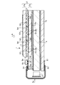
(参考例)
図7は接続線の参考例を示している。この参考例において、各接続線70は、少なくともその一部がシール材6の外側に位置する第1領域A1を有する。この第1領域A1は、境界線L4と、境界線L5と、境界線L6とによって囲まれる領域である。また、各接続線70は、シール材6の内側に位置する第2領域A2を有する。この第2領域A2は、境界線L2と走査線51の先端との間にある領域及び境界線L3と走査線51の先端との間にある領域である。
【0065】
また、各接続線70は、第1領域A1と第2領域A2とを接続する第3領域A3を有する。この第3領域A3は、前記境界線L2と、前記境界線L3と、前記境界線L4とによって囲まれる領域である。さらに、各接続線70は、第1領域A1と接続端子71とを接続する第4領域A4を有する。この第4領域A4は、前記境界線L5と、前記境界線L6と、接続端子71の列とによって囲まれる領域である。
【0066】
なお、複数の接続線70は、第1領域A1及び第2領域A2の個々の領域内においては互いに平行に配置されている。
【0067】
各接続線70の第1領域A1は、接続端子71の配列方向Yに対して小さい方の角度として第1角度β1を成している。また、第2領域A2は、配列方向Yに対して小さい方の角度として第2角度β2を成している。また、第3領域A3は、配列方向Yに対して小さい方の角度として第2角度β3を成している。また、第4領域A4は、配列方向Yに対して略直交している。そして、本実施形態では
β3>β1
β3>β2、そして
β1≠β2
に設定されている。
【0068】
また、図7において、接続線70は、シール材6が設けられた領域を境界として、走査線51に近接した領域である第2領域A2において、走査線51の延在方向に対して小さい方の角度α2で傾斜する方向に引き延ばされている。他方、接続線70は、端子71に近接した第1領域A1では、走査線51の延在方向に対して小さい方の角度α1で傾斜する方向に引き延ばされている。そして、α2>α1に設定されている。
第3領域A3及び第4領域A4では、複数の接続線70がそれぞれ走査線51と略平行に形成されている。また、シール材6は第1領域A1及び第2領域A2にかけて配置されている。
【0069】
接続線70に関する角度を以上のように設定することにより、複数の接続線70の第2領域A2同士の間隔は、第1領域A1同士の間隔よりも小さくなっている。つまり、接続線70の間隔は、シール材6の内側に形成された、走査線51に近接した第2領域A2で小さく、他方、シール材6の外側に形成された、端子71に近接した第1領域A1で、より大きくされている。
【0070】
以上により、シール材6の外側において接続線70にコロージョン等といった不良が発生することが防止されると共に、シール材6の内側で接続線70の角度を急峻にすることで、液晶パネル2の小型化を達成できる。
【0071】
図8は接続線の他の変形例を示している。この変形例において、各接続線70は、少なくともその一部がシール材6の外側に位置する第1領域A1を有する。この第1領域A1は、接続端子71に近い側で配列方向Yと平行に延びる境界線L0と、シール材6の内部において配列方向Yと平行に延びる境界線L1との間にある領域である。また、各接続線70は、シール材6の内側に位置する第2領域A2を有する。この第2領域A2は、前記境界線L1と走査線51の先端との間にある領域である。なお、本実施形態では、複数の接続線70は、第1領域A1及び第2領域A2内において、互いに平行とならないように形成されている。つまり、接続線70は例えば、境界線L0から境界線L1に向って、又は境界線L1から走査線51に向かって放射線状に広がるように形成されている。
【0072】
各接続線70の第1領域A1は、接続端子71の配列方向Yに対して小さい方の角度として第1角度β1を成している。また、第2領域A2は、配列方向Yに対して小さい方の角度として第2角度β2を成している。そして、本実施形態の場合、
β1>β2
に設定されている。
【0073】
また、図8において、接続線70は、シール材6が設けられた領域を境界として、走査線51に近接した領域である第2領域A2において走査線51の延在方向に対して全体として大きく傾いた角度α2で傾斜する方向に引き延ばされており、これに対して、端子71に近接した第1領域A1では走査線51の延在方向に対して、全体としてより小さな角度α1で傾斜する方向に引き延ばされている。つまり、
α2>α1
に設定されている。
【0074】
接続線70に関する角度を以上のように設定することにより、複数の接続線70の第2領域A2同士の間隔は、第1領域A1同士の間隔よりも小さくなっている。つまり、接続線70の間隔は、シール材6の内側に形成されていて走査線51に近接した第2領域A2で小さく、他方、シール材6の外側に形成されていて端子71に近接した第1領域A1で、より大きくされている。
【0075】
以上により、シール材6の外側において接続線70にコロージョン等といった不良が発生することが防止されると共に、シール材6の内側で接続線70の角度を急峻にすることで、液晶パネル2の小型化を達成できる。
【0076】
なお、図6〜図8に示した実施形態では、走査線51と液晶パネル駆動用IC8aとを接続する接続線の形状について説明したが、データ線52と液晶パネル駆動用IC8bとを接続する接続線80(図3参照)を上記接続線のいずれかと同様の形状に形成しても良い。
【0077】
(電子機器の実施形態)
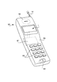
図9は、本発明に係る電子機器の一実施形態である携帯電話機を示している。ここに示す携帯電話機90は、アンテナ91、スピーカ92、液晶装置1、キースイッチ93、マイクロホン94等といった各種構成要素を、筐体としての外装ケース96に格納することによって構成される。また、外装ケース96の内部には、上記の各構成要素の動作を制御するための制御回路を搭載した制御回路基板97が設けられる。
【0078】
液晶装置1は図1に示す液晶装置等により構成される。なお、液晶装置1に代えて、本発明による他の液晶装置、あるいは液晶装置以外の電気光学装置を用いることができる。この携帯電話機90では、キースイッチ93及びマイクロホン94を通して入力される信号や、アンテナ91によって受信した受信データ等が制御回路基板97上の制御回路へ入力される。そしてその制御回路は、入力された各種データに基づいて液晶装置1の表示面内に数字、文字、絵柄等の画像を表示し、さらにアンテナ91を介して送信データを送信する。
【0079】
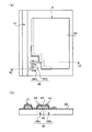
(電気光学装置の第2実施形態)
図10は、その液晶装置の一実施形態を示している。ここに示す液晶装置101は、図面の手前側に配置された第1の基板102aと、図面の奥側に配置された第2の基板102bとを環状のシール材103によって互いに接合、すなわち貼り合わせることによって形成される。
【0080】
シール材103、第1の基板102a及び第2の基板102bによって囲まれる領域は高さが一定の間隙、いわゆるセルギャップを構成する。さらに、シール材103の一部には液晶注入用開口103aが形成される。上記のセルギャップ内には、上記液晶注入用開口103aを通して液晶が注入され、その注入の完了後、液晶注入用開口103aが樹脂等によって封止される。
【0081】
図10において、第1の基板102aは第2の基板102bの外側へ張り出す基板張出し部102cを有し、その基板張出し部102c上に液晶パネル駆動用IC104a及び104bが導電接着要素、例えばACF(Anisotropic Conductive Film)106によって実装されている。液晶パネル駆動用IC104aと液晶パネル駆動用IC104bとは特性が異なるものであり、このように特性の異なる2種類の液晶パネル駆動用ICを用いるのは、第1の基板102a側と第2の基板102b側とで、換言すれば、走査線駆動系と信号線駆動系との間で使用する電圧値が異なっているため、それらを1つのICチップで賄うことができないからである。
【0082】
図11は、図10におけるII−II線に従って液晶装置101の断面構造を示している。図11において、第1の基板102aは基材109aを有し、その基材109aの内側表面、すなわち液晶L側の表面に複数の画素電極114aが形成される。また、図10に示すように、第1の基板102aの内側表面には、直線状の複数のライン配線132が互いに平行にストライプ状に形成され、それらのライン配線132に導通するようにTFD素子133が形成され、それらのTFD素子133を介して複数の画素電極114aがドットマトリクス状に形成される。また、画素電極114a、TFD素子133及びライン配線132の上に、図11に示すように、配向膜116aが形成される。また、基材109aの外側表面には位相差板117aが形成され、さらにその上に偏光板118aが形成される。
【0083】
図10及び図11において矢印IVで示す1個のTFD素子の近傍の構造を示すと、例えば図12の通りである。図12に示すのは、いわゆるBack-to-Back(バック・ツー・バック)構造のTFD素子を用いたものである。図12において、ライン配線132は、例えば、TaW(タンタル・タングステン)によって形成された第1層132aと、例えば陽極酸化膜であるTa2O5(酸化タンタル)によって形成された第2層132bと、例えばCrによって形成された第3層132cとから成る3層構造に形成されている。
【0084】
また、TFD素子133は、第1TFD部133aと第2TFD部133bとを直列に接続することによって構成されている。第1TFD部133a及び第2TFD部133bは、TaWによって形成された第1金属層136と、陽極酸化によって形成されたTa2O5の絶縁層137と、ライン配線132の第3層132cと同一層であるCrの第2金属層138との3層積層構造によって構成されている。
【0085】
第1TFD部133aをライン配線132側から見ると、第2金属層138/絶縁層137/第1金属層136の積層構造が構成され、他方、第2TFD部133bをライン配線132側から見ると、第1金属層136/絶縁層137/第2金属層138の積層構造が構成される。このように一対のTFD部133a及び133bを電気的に逆向きに直列接続してバック・ツー・バック構造のTFD素子を構成することにより、TFD素子のスイッチング特性の安定化が達成されている。画素電極114aは、第2TFD部133bの第2金属層138に導通するように、例えばITOによって形成される。
【0086】
図11において、第2の基板102bは基材109bを有し、その基材109bの内側表面、すなわち液晶L側の表面には半透過反射膜11が形成され、その上にカラーフィルタ膜112が形成され、その上にオーバーコート膜113が形成され、その上に第2電極114bが形成され、さらにその上に配向膜116bが形成される。また、基材109bの外側表面には、位相差板117bが形成され、さらにその上に偏光板118bが形成される。
【0087】
また、第2の基板102bに対向して導光体123が配置され、その導光体123の1辺に対向して発光源としてのLED124が配置される。導光体123及びLED124は、バックライトとして作用する照明装置126を構成する。第2電極114bは、図10に示すように、多数の直線状の電極をライン配線132と交差するように互いに平行に並べることによりストライプ状に形成されている。なお、図10では、電極パターンをわかり易く示すために、第2電極114bの間隔を大きく広げて模式的に描いてあるが、実際には、第2電極114bの間隔は画素電極114aのドットピッチに合せて非常に狭く形成されている。
【0088】
画素電極114aと第2電極114bとの交差点はドットマトリクス状に配列しており、これらの交差点の個々がそれぞれ1つのドットを構成し、図11のカラーフィルタ膜112の個々の色パターンがその1ドットに対応する。カラーフィルタ膜112は、例えば、R(赤)、G(緑)、B(青)の3原色が1つのユニットとなって1画素を構成する。つまり、3ドットが1つのユニットになって1つの画素を構成している。
【0089】
基材109a,109bは、例えば、ガラス、プラスチック等によって形成される。また、半透過反射膜111は光反射性の材料、例えば、Al(アルミニウム)によって形成される。なお、半透過反射膜111によって光透過性及び光反射性の両機能を達成するためには、例えば、半透過反射膜111の膜厚を薄くしたり、半透過反射膜111の適所に光透過用の穴を開ける等といった措置が施される。
【0090】
カラーフィルタ膜112は、周知の色絵素形成手法、例えば、インクジェット法、顔料分散法等を用いて顔料を、モザイク配列、ストライプ配列、デルタ配列等といった適宜のパターンに塗布することによって形成される。また、オーバーコート膜113は、適宜の透光性樹脂材料を、例えばスピンコート法、ロールコート法等によって均一に塗布することによって形成される。
【0091】
電極114a及び114bは、例えば、ITO(Indium Tin Oxide)を周知の膜付け法、例えば、スパッタ法、真空蒸着法を用いて膜付けし、さらにフォトエッチング法によって希望のパターンに形成される。配向膜116a,116bは、例えば、ポリイミド溶液を塗布した後に焼成する方法や、オフセット印刷法等によって形成される。
【0092】
図10において、第1の基板102a上には、ライン配線132からそのまま延びる接続線119aと、シール材の中に分散された導通材121を介して第2の基板102b上の第2電極114bに接続される接続線119bとが形成される。また、基板張出し部102cの辺端部には端子122が形成される。
【0093】
図11では、液晶装置101の全体をわかり易く示すために、導通材121を断面楕円状に模式化して示してあるが、実際は、導通材121は球状又は円筒状に形成され、その大きさはシール材103の線幅に対して非常に小さいものである。よって、導通材121はシール材103の線幅方向に複数個存在することができる。
【0094】
本実施形態に係る液晶装置101は以上のように構成されているので、この液晶装置101は反射型表示及び透過型表示の両方によって表示を行う。反射型表示では、図11において第1の基板102a側の外部から取り込んだ光を半透過反射膜111によって反射させて液晶Lの層へ供給する。一方、透過型表示では、照明装置126のLED124で発光した光が導光体123によって面状の光として広げられて第2の基板102bへ供給され、さらに半透過反射膜111等を通過して液晶Lの層へ供給される。
【0095】
光が液晶Lの層へ供給されるとき、液晶Lに印加する電圧を画素毎に制御して液晶の配向を画素毎に制御することにより、液晶Lの層へ供給された光を画素毎に変調し、その変調した光を偏光板118aへ供給する。これにより、第1の基板102aの外側へ文字等といった像を表示する。この像は、ドットマトリクス状に配列された画素電極114aとこれに対向する対向電極114bとが重なった部分に形成されるピクセルによって平面的に区画される領域である、駆動領域すなわち表示領域Vの中に形成される。
【0096】
図13は、図10に符号IIIで示す接続線119bの部分を拡大して示している。図示の通り、接続線119bは、ライン配線132と略平行な直線領域120aと、それに続いて傾斜する第2領域120bと、それに続く第3領域120cと、それに続く第1領域120dと、それに続く第4領域120eとを有する。最後の第4領域120eは、液晶パネル駆動用IC104bのバンプに導電接続する端子108につながっている。接続線119bの各領域120a〜120eは、いずれも隣り合う線同士が互いに略平行になっている。
【0097】
接続線119bの直線領域120a同士の間隔は、第2領域120bによって広げられて、第3領域120cの間隔となっている。また、接続線119bの第3領域120cの間隔は、第1領域120dによって広げられて第4領域120eとなっている。
【0098】
シール材103の外側に位置する領域、すなわち第3領域120c,第1領域120d及び第4領域120eの各領域同士の間隔は、シール材103の内側に位置する領域、すなわち領域120a及び第2領域120bの各領域同士の間隔よりも大きくなっている。この結果、シール材103の外側では、接続線119bの間隙幅、すなわち隣り合う接続線119bの間に形成される間隙の幅を大きくすることができるので、それらの接続線119bにコロージョン、すなわち電食が発生することを防止できる。一方、シール材103の内側では、接続線119bの間隔を小さくできるので、接続線119bの全体の幅を小さくでき、それ故、液晶装置の全体の平面的な外形形状を小さくできる。
【0099】
なお、接続端子108の配列方向Yに対する次の各角度、すなわち、第2領域120bの角度を第2角度β2、第3領域120cの角度を第3角度β3、そして第4領域120eの角度を第4角度β4とすると、
β3>β1
β3>β2、そして
β1≠β2
である。
【0100】
また、図13では、シール材103を通過する接続線119bの間隔、すなわち第3領域120c及び第1領域120dの間隔が、シール材103の内側における接続線119bの間隔、すなわち直線領域120a及び第2領域120bの間隔よりも大きく設定されている。また、図13では、一実施形態としてβ2>β1と設定しているが、β1>β2と設定すれば、上述した他の実施形態と同様に、シール材6の内側で接続線70の角度を急峻にすることで、液晶パネル2の小型化を達成できる。
【0101】
本実施形態の液晶装置では、シール材103の中に混入した導通材121によって、第1の基板102a上の接続線119bと第2の基板102b上の第2電極114bとの間の導通をとっている。シール材103を通過する接続線119bの間隙幅、すなわちギャップが小さいと、シール材103を通過する接続線119bが導通材121によってショート、すなわち短絡するおそれがある。これに対し、上記のようにシール材103を通過する接続線119bの間隔、すなわち第3領域120c及び第1領域120dの間隔を大きく設定しておけば、それらの接続線119bが導通材121によってショートすることを防止できる。
【0102】
(その他の実施形態)
以上、好ましい実施形態を挙げて本発明を説明したが、本発明はその実施形態に限定されるものでなく、請求の範囲に記載した発明の範囲内で種々に改変できる。
【0103】
例えば、図1や図10では、バック・ツー・バック構造のTFD素子をスイッチング素子とするアクティブマトリクス方式の液晶装置を例示したが、本発明は、単一のTFD素子をスイッチング素子とする液晶装置に適用することもできる。また、本発明は、TFD素子に代えてTFT(Thin Film Transistor)素子をスイッチング素子とするアクティブマトリクス方式の液晶装置に適用することもできる。また、本発明は、スイッチング素子を用いない構造の単純マトリクス方式の液晶装置にも適用できる。
【0104】
また、以上の説明では電気光学装置として液晶装置を例示したが、これ以外に、有機EL装置、プラズマディスプレイ等といった他の電気光学装置にも本発明を適用できる。また、以上の説明では電子機器として携帯電話機を例示したが、これ以外に、携帯情報端末機、ビデオカメラ等といった他の電子機器にも本発明を適用できる。
【0105】
【発明の効果】
本発明に係る電気光学装置及び電子機器によれば、シール材の内側における接続線の間隔が、シール材の外側における接続線の間隔よりも小さいので、コロージョン等といった不良が発生するおそれのあるシール材の外側の領域では、接続線の間隔を大きくでき、結果的に接続線の間隙幅を大きくすることができ、これにより、コロージョン等の発生を防止できる。
【0106】
他方、コロージョン等といった不良が発生するおそれのないシール材の内側の領域では、接続線の間隔を小さくすることができ、このように接続線の間隔を小さくすれば、表示領域と接続端子との間の距離を小さくすることができる。そしてこれにより、電気光学装置の平面的な外形形状を小さくすることができる。
【図面の簡単な説明】
【図1】 本発明に係る電気光学装置の一例である液晶装置の一実施形態を分解して示す斜視図である。
【図2】 図1に示す液晶装置の断面構造を示す断面図である。
【図3】 図1に示す液晶装置を構成する液晶パネルの等価回路図である。
【図4】 図1に示す液晶装置の画素の構成を示す図であり、(a)は平面図、(b)は(a)のB−B線に従った断面図である。
【図5】 図1の液晶装置で用いられる接続線の一例を示す平面図である。
【図6】 図1の液晶装置で用いられる接続線の他の一例を示す平面図である。
【図7】 図1の液晶装置で用いられる接続線のさらに他の参考例を示す平面図である。
【図8】 図1の液晶装置で用いられる接続線のさらに他の一例を示す平面図である。
【図9】 本発明に係る電子機器の一実施形態である携帯電話機の一例を示す斜視図である。
【図10】 本発明に係る電気光学装置の一例である液晶装置の他の実施形態を一部破断して示す平面図である。
【図11】 図10におけるII−II線に従って液晶装置の断面構造を示す断面図である。
【図12】 図10に示す液晶装置の1つの画素部分を示す斜視図である。
【図13】 図10の液晶装置における矢印IIIで示す部分を拡大して示す図である。
【図14】 接続線と接続端子との関係を示す図であり、(a)は接続線が接続端子の配列方向に対して直角方向へ延びる領域を含む場合、(b)は接続線が接続端子の配列方向に対して斜め方向に延びる場合を示している。[0001]
BACKGROUND OF THE INVENTION
The present invention relates to an electro-optical device in which a display region formed inside a seal material and a connection terminal formed outside the seal material are connected by a plurality of connection lines, and an electronic apparatus using the same.
[0002]
[Prior art]
In a liquid crystal device in which liquid crystal is sealed between a pair of substrates, the pair of substrates is overlapped and bonded by a sealing material disposed around the display region. Liquid crystal is sealed in a region inside the sealing material between the pair of substrates. In the matrix type liquid crystal device, one end of a connection line formed on the substrate is connected to each of the plurality of display lines arranged in parallel to the display region, and the connection line is drawn out to the outside of the sealing material. A connection terminal is formed at the other end of the connection line. In a so-called COG (Chip On Glass) type liquid crystal device, an output terminal of the liquid crystal panel driving IC, that is, a bump is connected to the connection terminal.
[0003]
In general, the distance between the bumps of the liquid crystal panel driving IC and the distance between the display lines in the display area are not the same. Therefore, the distance between the bumps and the connection lines connecting the display lines is from the bumps toward the display lines, It is formed in a shape that expands in the opposite direction.
[0004]
In the present specification, “interval” refers to the pitch between adjacent objects. “Gap width” refers to the width of a gap formed between adjacent objects.
[0005]
[Problems to be solved by the invention]
Usually, the interval between the bumps of the liquid crystal panel driving IC is determined irrespective of the width of the display area. For this reason, when the width or area of the display region is set to be large, the difference between the interval between the display lines constituting the display region and the interval between the bumps of the liquid crystal panel driving IC is remarkably increased. In particular, when using a liquid crystal panel driving IC having a narrow bump spacing, the difference in the spacing becomes more significant.
[0006]
The difference between these intervals can be eliminated by forming the connection lines obliquely so that the interval between the connection lines expands in a predetermined direction, but the inclination angle of the connection lines is limited. That is, if the inclination angle is increased too much, the gap between the connection lines is narrowed, and in particular, the gap width between adjacent connection lines is narrowed. Therefore, there is a risk of occurrence of defects such as corrosion. That is, there is a limit to increasing the inclination angle of the connection line.
[0007]
Further, if the inclination angle of the connection line is reduced, the above-mentioned corrosion problem is solved. However, in this case, the distance between the display area and the liquid crystal panel driving IC increases as the inclination angle is reduced. As a result, a necessary mounting space is increased around the display area, and the liquid crystal device becomes larger than the display area.
[0008]
SUMMARY An advantage of some aspects of the invention is that it provides an electro-optical device and an electronic apparatus that can achieve downsizing while suppressing occurrence of defects such as corrosion.
[0009]
[Means for Solving the Problems]
(1) In order to achieve the above object, an electro-optical device according to the present invention includes a first substrate and a second substrate that are overlaid on each other, and the first substrate and the second substrate that are overlapped with each other in a display region. A sealing material that is bonded to the periphery of the first substrate, a plurality of connection terminals that are provided to extend from the second substrate, and are provided on the first substrate. A plurality of connection lines connecting the region and the plurality of connection terminals, wherein an interval between the connection lines inside the sealing material is smaller than an interval between the connection lines outside the sealing material, To do.
[0010]
According to this electro-optical device, since the interval between the connection lines inside the seal material is smaller than the interval between the connection lines outside the seal material, in the region outside the seal material where a defect such as corrosion may occur. The interval between the connecting lines can be increased, and as a result, the gap width between the connecting lines can be increased, thereby preventing the occurrence of corrosion and the like.
[0011]
On the other hand, in the area inside the sealing material where there is no possibility of occurrence of defects such as corrosion, the distance between the connection lines can be reduced. If the distance between the connection lines is reduced in this way, the display area and the connection terminal The distance between them can be reduced. As a result, the planar outer shape of the electro-optical device can be reduced.
[0012]
That is, according to the electro-optical device having the above-described configuration, it is possible to reduce the planar outer shape of the electro-optical device while suppressing the occurrence of defects such as corrosion. In the above configuration, in the region inside the sealing material, the interval between the connection lines can be made as small as possible in manufacturing, for example, the interval determined by the resolution of the resist in the patterning process. Further, in the region outside the sealing material, the interval between the connection lines can be determined so that a gap width between the connection lines can be secured to a degree that can prevent occurrence of defects such as corrosion.
[0013]
In the above configuration, the connection terminal may be connected to a bump of an electro-optical panel driving IC, or may be connected to a terminal formed on a flexible printed board. When a terminal formed on the flexible printed board is connected, the electro-optical device is connected to an external circuit via the connection terminal.
[0014]
Specifically, the electro-optical device having the above configuration can be widely applied to various electro-optical devices such as a liquid crystal device, a plasma display device, an electroluminescence display device, and the like.
[0015]
(2) Next, another electro-optical device according to the present invention includes a first substrate and a second substrate that are overlaid on each other, and the first substrate and the second substrate that surround the display region. A sealing material to be joined, a plurality of connection terminals provided on the extension portion of the first substrate formed to extend from the second substrate, and provided on the first substrate and formed in the display region A plurality of connection lines that connect each of the plurality of display lines and each of the plurality of connection terminals, and the interval between the connection lines inside the sealing material is the connection lines outside the sealing material. It is smaller than the interval.
[0016]
The electro-optical device having this configuration is different from the electro-optical device having the configuration described in the above item (1) in that “a plurality of display lines are formed in the display area and the connection lines are connected to the display lines”. There is a difference.
[0017]
According to this electro-optical device, since the interval between the connection lines inside the seal material is smaller than the interval between the connection lines outside the seal material, in the region outside the seal material where a defect such as corrosion may occur. The interval between the connecting lines can be increased, and as a result, the gap width between the connecting lines can be increased, thereby preventing the occurrence of corrosion and the like.
[0018]
On the other hand, in the area inside the sealing material where there is no possibility of occurrence of defects such as corrosion, the distance between the connection lines can be reduced. If the distance between the connection lines is reduced in this way, the display area and the connection terminal The distance between them can be reduced. As a result, the planar outer shape of the electro-optical device can be reduced.
[0019]
That is, according to the electro-optical device having the above-described configuration, it is possible to reduce the planar outer shape of the electro-optical device while suppressing the occurrence of defects such as corrosion. In the above configuration, in the region inside the sealing material, the interval between the connection lines can be made as small as possible in manufacturing, for example, the interval determined by the resolution of the resist in the patterning process. Further, in the region outside the sealing material, the interval between the connection lines can be determined so that a gap width between the connection lines can be secured to a degree that can prevent occurrence of defects such as corrosion.
[0020]
In the above configuration, the connection terminal may be connected to a bump of an electro-optical panel driving IC, or may be connected to a terminal formed on a flexible printed board. When a terminal formed on the flexible printed board is connected, the electro-optical device is connected to an external circuit via the connection terminal.
[0021]
Specifically, the electro-optical device having the above configuration can be widely applied to various electro-optical devices such as a liquid crystal device, a plasma display device, an electroluminescence display device, and the like.
[0022]
(3) Next, in another electromechanical device according to the present invention, in the electro-optical device having the configuration described in the above item (2), an inclination angle of the connection line inside the seal material with respect to the display line is It is larger than the inclination angle with respect to the display line of the connection line outside the sealing material.
[0023]
In this case, the distance between the connection lines can be greatly changed inside the sealing material while suppressing the length of the connection line in the extending direction of the display line. Moreover, the space | interval of a connection line can be expanded outside a sealing material.
[0024]
(4) Next, another electro-optical device according to the present invention is the electro-optical device having the configuration described in the above (2) or (3), wherein the interval between the connection terminals is the interval between the display lines. It is characterized by being smaller than
(5) Next, another electro-optical device according to the present invention is the electro-optical device having the configuration described in (1) to (4) above, wherein the connection terminal includes an electro-optical panel driving IC. An output terminal is connected. In this case, the interval between the connection terminals is the same as the interval between the output terminals of the electro-optical panel driving IC. In addition, as an electro-optical panel, a liquid crystal panel, an organic EL panel, etc. can be considered.
[0025]
(6) Next, another electro-optical device according to the present invention is the electro-optical device having the configuration described in the items (1) to (5), wherein the gap between the connection lines outside the sealing material. The width is larger than the gap width between the connection lines inside the sealing material. In this case, the occurrence of defects such as corrosion can be effectively prevented by enlarging the gap width between the connection lines outside the seal material.
[0026]
(7) Next, an electronic apparatus according to the present invention is an electronic apparatus that includes an electro-optical device, a housing that houses the electro-optical device, and a control unit that controls the operation of the electro-optical device. The optical device is constituted by the electro-optical device having the configuration described in the above items (1) to (6). As such an electronic device, for example, a mobile phone, a portable information terminal, and the like can be considered.
[0027]
(8) Next, another electro-optical device according to the present invention includes a first substrate and a second substrate that are overlaid on each other, and the first substrate and the second substrate that surround the display region. A sealing material to be joined, a conductive material mixed in the sealing material, a plurality of connection terminals provided on a protruding portion of the first substrate formed to protrude from the second substrate, and the first A plurality of connection lines provided on one substrate, connected to the plurality of connection terminals and extending through the seal material, and an interval between the connection lines inside the seal material is It is smaller than the interval between the connection lines on the outer side, and further, the interval between the connection lines passing through the sealing material is larger than the interval between the connection lines inside the sealing material.
[0028]
According to this electro-optical device, the conductive material formed on the first substrate and the conductive pattern formed on the second substrate are connected to the conductive material by the conductive material present in the sealing material. Can be electrically connected.
[0029]
Further, according to this electro-optical device, since the interval between the connecting lines in the portion that passes through the sealing material is increased, the conductive material that is included in the sealing material includes the adjacent connecting lines in the portion that passes through the sealing material. Therefore, it is possible to prevent a short circuit, that is, a short circuit.
[0030]
(9) Next, another electro-optical device according to the present invention includes a substrate, an electro-optical layer supported by the substrate and disposed at least in a display area, and a sealing material provided around the electro-optical layer. And a plurality of connection terminals provided at an end portion of the substrate, and a plurality of connection lines provided on the substrate and connecting the display region and the plurality of connection terminals, The connection line inside the sealing material is bent inside the outer periphery of the sealing material so as to be smaller than the space between the connection lines outside the sealing material. To do.
[0031]
(10) Next, another electro-optical device according to the present invention includes a substrate, an electro-optical layer supported by the substrate and disposed at least in a display region, and a sealing material provided around the electro-optical layer. And a plurality of connection terminals provided at end portions of the substrate and arranged along a predetermined direction, and a plurality of connection lines provided on the substrate and formed in the display region and the plurality of connections. A plurality of connection lines connecting each of the terminals, each of the plurality of connection lines has a first region and a second region, and at least a part of the first region is the It is located outside the sealing material and forms a first angle as a smaller angle with respect to the predetermined direction, and the second region is located inside the sealing material and is located with respect to the predetermined direction. Second angle as the smaller angle The second angle is smaller than the first angle, and the interval between the connection lines in the second region is smaller than the interval between the connection lines in the first region. To do.
[0032]
(11) Next, another electro-optical device according to the present invention includes a substrate, an electro-optical layer supported by the substrate and disposed at least in a display region, and a sealing material provided around the electro-optical layer. And a plurality of connection terminals provided at an end of the substrate and arranged along a predetermined direction, and a plurality of connection lines provided on the substrate and connected to the plurality of connection terminals, Each of the plurality of connection lines has a first region, a second region, and a third region. At least a part of the first region is located outside the sealing material, and the predetermined direction A first angle is formed as a smaller angle with respect to the second region, and the second region is located inside the sealing material, and a second angle is formed as a smaller angle with respect to the predetermined direction. And the third region is the first region. And is connected to the second region and forms a third angle as a smaller angle with respect to the predetermined direction, and the third angle is greater than the first angle and the second angle. The first angle and the second angle are different from each other, and the interval between the connection lines in the second region is smaller than the interval between the connection lines in the first region. .
[0033]
(12) Next, according to another electro-optical device according to the invention, in the electro-optical device having the configuration described in the above item (11), each of the plurality of connection lines further includes a fourth region, The fourth region is connected to the first region and the connection terminal, and is substantially orthogonal to the predetermined direction.
[0034]
In the electro-optical device having this configuration, the fourth region A4 of the
[0035]
In consideration of connecting the
[0036]
At this time, if the
[0037]
(13) Next, another electro-optical device according to the present invention is the electro-optical device having the configuration described in the above item (12), in which the third angle is approximately 90 °.
[0038]
(14) Next, another electro-optical device according to the present invention is the electro-optical device having the configuration described in the above item (11), in which the second angle is smaller than the first angle. And
[0039]
(15) Next, another electro-optical device according to the present invention is the electro-optical device having the configuration described in the above item (11), in which the two adjacent connection lines among the plurality of connection lines are: The first, second and third regions are arranged substantially parallel to each other.
[0040]
(16) Next, another electro-optical device according to the present invention includes a substrate, an electro-optical layer supported by the substrate and disposed at least in a display region, and a sealing material provided around the electro-optical layer. A plurality of connection terminals provided at an end of the substrate, and a plurality of connection terminals provided on the substrate and connected to each of the plurality of display lines and each of the plurality of connection terminals. Each of the plurality of connection lines has a first region and a second region, and at least a part of the first region is located outside the sealing material, A first angle is formed as a smaller angle with respect to the display line, and the second region is located inside the sealing material, and a second angle is formed as a smaller angle with respect to the display line. The plurality of connections Each of the lines, as the second angle is greater than the first angle, characterized in that it is bent at a boundary between the first region and the second region.
[0041]
DETAILED DESCRIPTION OF THE INVENTION
(First embodiment of electro-optical device)
Hereinafter, an embodiment in which the electro-optical device according to the invention is applied to an active matrix type liquid crystal device will be described.
[0042]
1 is an exploded perspective view of a liquid crystal device as an example of an electro-optical device, FIG. 2 is a cross-sectional view of the liquid crystal device, and FIG. 3 is an equivalent circuit diagram of the liquid crystal device. 4 shows the structure of one of a plurality of pixels constituting the display area of the liquid crystal device. In particular, FIG. 4A shows a plan view of the pixel, and FIG. A sectional view according to line B is shown.
[0043]
As shown in FIGS. 1 and 2, the
[0044]
The
[0045]
In FIG. 1, the
[0046]
As shown in FIG. 2, a plurality of
[0047]
Various optical elements are provided on the first substrate 7a and the
[0048]
As shown in FIG. 3, the
[0049]
The
[0050]
The
[0051]
As shown in FIG. 4, the
[0052]
The individual
[0053]
As shown in FIG. 5, one end of a
[0054]
FIG. 5 conceptually shows the shape of the
[0055]
The first region A1 of each
β1> β2
Is set to
[0056]
Further, in FIG. 5, the
α2> α1
Is set to
[0057]
By setting the angle related to the
[0058]
In general, defects such as corrosion may occur on the outside of the sealing material. However, as described above, if the distance between the connection lines 70 is set large on the outside of the sealing
[0059]
FIG. 6 shows a modification of the connection line. In this modification, each
β1> β2
Is set to
[0060]
In this embodiment, β1≈90 ° is set. The plurality of
[0061]
In FIG. 6, the connecting
[0062]
By setting the angle related to the
[0063]
As a result, the occurrence of defects such as corrosion in the
[0064]
(Reference example)
Figure 7 shows the connection linesReference exampleIs shown. thisReference exampleIn FIG. 5, each
[0065]
Each
[0066]
Note that the plurality of
[0067]
The first region A1 of each
β3> β1
β3> β2, and
β1 ≠ β2
Is set to
[0068]
Further, in FIG. 7, the
In the third region A3 and the fourth region A4, a plurality of
[0069]
By setting the angle related to the
[0070]
As a result, the occurrence of defects such as corrosion in the
[0071]
FIG. 8 shows another modification of the connection line. In this modification, each
[0072]
The first region A1 of each
β1> β2
Is set to
[0073]
In FIG. 8, the connecting
α2> α1
Is set to
[0074]
By setting the angle related to the
[0075]
As a result, the occurrence of defects such as corrosion in the
[0076]
In the embodiment shown in FIGS. 6 to 8, the shape of the connection line connecting the
[0077]
(Embodiment of electronic device)
FIG. 9 shows a mobile phone which is an embodiment of an electronic apparatus according to the present invention. A
[0078]
The
[0079]
(Second embodiment of electro-optical device)
FIG. 10 shows an embodiment of the liquid crystal device. In the
[0080]
A region surrounded by the sealing
[0081]
In FIG. 10, the
[0082]
FIG. 11 shows a cross-sectional structure of the
[0083]
The structure in the vicinity of one TFD element indicated by an arrow IV in FIGS. 10 and 11 is, for example, as shown in FIG. FIG. 12 shows a so-called back-to-back (back-to-back) structure TFD element. In FIG. 12, the
[0084]
The
[0085]
When the
[0086]
In FIG. 11, the
[0087]
Further, a
[0088]
Intersections between the
[0089]
The
[0090]
The color filter film 112 is formed by applying a pigment in an appropriate pattern such as a mosaic arrangement, a stripe arrangement, or a delta arrangement by using a known color picture element forming method, for example, an inkjet method, a pigment dispersion method, or the like. The overcoat film 113 is formed by uniformly applying an appropriate translucent resin material by, for example, a spin coat method, a roll coat method, or the like.
[0091]
The
[0092]
In FIG. 10, on the
[0093]
In FIG. 11, in order to show the entire
[0094]
Since the
[0095]
When light is supplied to the layer of liquid crystal L, the voltage applied to the liquid crystal L is controlled for each pixel, and the orientation of the liquid crystal is controlled for each pixel. The modulated light is supplied to the
[0096]
FIG. 13 shows an enlarged view of the connecting
[0097]
The interval between the
[0098]
The area located outside the sealing
[0099]
It should be noted that the following angles with respect to the arrangement direction Y of the
β3> β1
β3> β2, and
β1 ≠ β2
It is.
[0100]
In FIG. 13, the interval between the
[0101]
In the liquid crystal device of this embodiment, the
[0102]
(Other embodiments)
The present invention has been described with reference to the preferred embodiments. However, the present invention is not limited to the embodiments, and various modifications can be made within the scope of the invention described in the claims.
[0103]
For example, in FIGS. 1 and 10, an active matrix type liquid crystal device using a back-to-back structure TFD element as a switching element is illustrated, but the present invention is a liquid crystal device using a single TFD element as a switching element. It can also be applied to. The present invention can also be applied to an active matrix type liquid crystal device in which a TFT (Thin Film Transistor) element is used as a switching element instead of a TFD element. The present invention can also be applied to a simple matrix type liquid crystal device having a structure in which no switching element is used.
[0104]
In the above description, the liquid crystal device is exemplified as the electro-optical device, but the present invention can also be applied to other electro-optical devices such as an organic EL device and a plasma display. In the above description, a mobile phone is exemplified as the electronic device. However, the present invention can be applied to other electronic devices such as a portable information terminal and a video camera.
[0105]
【The invention's effect】
According to the electro-optical device and the electronic apparatus according to the present invention, since the interval between the connection lines inside the sealing material is smaller than the interval between the connection lines outside the sealing material, there is a possibility that a defect such as corrosion may occur. In the region outside the material, the interval between the connection lines can be increased, and as a result, the gap width of the connection lines can be increased, thereby preventing the occurrence of corrosion or the like.
[0106]
On the other hand, in the area inside the sealing material where there is no possibility of occurrence of defects such as corrosion, the distance between the connection lines can be reduced. If the distance between the connection lines is reduced in this way, the display area and the connection terminal The distance between them can be reduced. As a result, the planar outer shape of the electro-optical device can be reduced.
[Brief description of the drawings]
FIG. 1 is an exploded perspective view showing an embodiment of a liquid crystal device which is an example of an electro-optical device according to the invention.
2 is a cross-sectional view showing a cross-sectional structure of the liquid crystal device shown in FIG.
FIG. 3 is an equivalent circuit diagram of a liquid crystal panel constituting the liquid crystal device shown in FIG.
4A and 4B are diagrams illustrating a configuration of a pixel of the liquid crystal device illustrated in FIG. 1, in which FIG. 4A is a plan view, and FIG. 4B is a cross-sectional view taken along line BB in FIG.
FIG. 5 is a plan view showing an example of connection lines used in the liquid crystal device of FIG. 1;
FIG. 6 is a plan view showing another example of connection lines used in the liquid crystal device of FIG.
7 is still another connection line used in the liquid crystal device of FIG.Reference exampleFIG.
FIG. 8 is a plan view showing still another example of connection lines used in the liquid crystal device of FIG. 1;
FIG. 9 is a perspective view showing an example of a mobile phone which is an embodiment of the electronic apparatus according to the invention.
FIG. 10 is a plan view partially broken away showing another embodiment of a liquid crystal device which is an example of an electro-optical device according to the invention.
11 is a cross-sectional view showing a cross-sectional structure of the liquid crystal device according to the line II-II in FIG.
12 is a perspective view showing one pixel portion of the liquid crystal device shown in FIG.
13 is an enlarged view showing a portion indicated by an arrow III in the liquid crystal device of FIG.
14A and 14B are diagrams showing a relationship between a connection line and a connection terminal, in which FIG. 14A shows a case where the connection line includes a region extending in a direction perpendicular to the arrangement direction of the connection terminals, and FIG. The case where it extends in the diagonal direction with respect to the arrangement direction of a terminal is shown.
Claims (7)
基板と、
表示領域の周囲に設けられたシール材と、
前記基板の端部に設けられ、所定の方向に沿って配列された複数の接続端子と、
前記基板に設けられ、前記複数の接続端子に接続される複数の接続線と、
を備え、
前記複数の接続線の各々は、第1領域、第2領域及び第3領域を有しており、
前記第1領域は、少なくともその一部が前記シール材の外側に位置するとともに、前記所定の方向に対する小さい方の角度として第1の角度を成しており、
前記第2領域は、前記シール材の内側に位置するとともに、前記所定の方向に対する小さい方の角度として第2の角度を成しており、
前記第3領域は、前記第1領域及び前記第2領域に接続されるとともに、前記所定の方向に対する小さい方の角度として第3の角度を成しており、
前記第3の角度は、前記第1の角度および前記第2の角度よりも大きく、
前記第1の角度および前記第2の角度は互いに異なっており、
前記第2領域における前記接続線の間隔が、前記第1領域における前記接続線の間隔よりも小さいことを特徴とする電気光学装置。In an electro-optical device,
A substrate,
Sealing material provided around the display area;
A plurality of connection terminals provided at an end of the substrate and arranged along a predetermined direction;
A plurality of connection lines provided on the substrate and connected to the plurality of connection terminals;
With
Each of the plurality of connection lines has a first region, a second region, and a third region,
The first region is at least partially located outside the sealing material, and forms a first angle as a smaller angle with respect to the predetermined direction,
The second region is located inside the seal material and forms a second angle as a smaller angle with respect to the predetermined direction,
The third region is connected to the first region and the second region, and forms a third angle as a smaller angle with respect to the predetermined direction,
The third angle is greater than the first angle and the second angle;
The first angle and the second angle are different from each other;
An electro-optical device, wherein an interval between the connection lines in the second region is smaller than an interval between the connection lines in the first region.
前記複数の接続線の各々は、第4領域を更に有し、
前記第4領域は、前記第1領域及び前記接続端子に接続されるとともに、前記所定の方向に対して略直交していることを特徴とする電気光学装置。In claim 1,
Each of the plurality of connection lines further includes a fourth region,
The electro-optical device, wherein the fourth region is connected to the first region and the connection terminal, and is substantially orthogonal to the predetermined direction.
Priority Applications (1)
| Application Number | Priority Date | Filing Date | Title |
|---|---|---|---|
| JP2001261578A JP3829669B2 (en) | 2000-09-22 | 2001-08-30 | Electro-optical device and electronic apparatus |
Applications Claiming Priority (3)
| Application Number | Priority Date | Filing Date | Title |
|---|---|---|---|
| JP2000-288463 | 2000-09-22 | ||
| JP2000288463 | 2000-09-22 | ||
| JP2001261578A JP3829669B2 (en) | 2000-09-22 | 2001-08-30 | Electro-optical device and electronic apparatus |
Publications (3)
| Publication Number | Publication Date |
|---|---|
| JP2002169488A JP2002169488A (en) | 2002-06-14 |
| JP2002169488A5 JP2002169488A5 (en) | 2005-06-09 |
| JP3829669B2 true JP3829669B2 (en) | 2006-10-04 |
Family
ID=26600510
Family Applications (1)
| Application Number | Title | Priority Date | Filing Date |
|---|---|---|---|
| JP2001261578A Expired - Lifetime JP3829669B2 (en) | 2000-09-22 | 2001-08-30 | Electro-optical device and electronic apparatus |
Country Status (1)
| Country | Link |
|---|---|
| JP (1) | JP3829669B2 (en) |
Families Citing this family (6)
| Publication number | Priority date | Publication date | Assignee | Title |
|---|---|---|---|---|
| JP4683827B2 (en) * | 2003-09-25 | 2011-05-18 | 京セラ株式会社 | Liquid crystal display |
| JP2007322488A (en) * | 2006-05-30 | 2007-12-13 | Optrex Corp | Display panel |
| JP4518199B2 (en) * | 2007-10-23 | 2010-08-04 | エプソンイメージングデバイス株式会社 | Electro-optic device |
| TWI492201B (en) * | 2007-10-23 | 2015-07-11 | Japan Display Inc | Electro-optical device |
| CN103635949B (en) * | 2011-07-20 | 2015-12-09 | 夏普株式会社 | Active-matrix substrate and the display panel possessing it |
| TWI536130B (en) * | 2014-12-05 | 2016-06-01 | 群創光電股份有限公司 | Display panel and electronic display device |
-
2001
- 2001-08-30 JP JP2001261578A patent/JP3829669B2/en not_active Expired - Lifetime
Also Published As
| Publication number | Publication date |
|---|---|
| JP2002169488A (en) | 2002-06-14 |
Similar Documents
| Publication | Publication Date | Title |
|---|---|---|
| KR100425052B1 (en) | Electro-optical device and electronic equipment | |
| US6919948B2 (en) | Liquid crystal panel, manufacturing method therefor, and electronic equipment | |
| US8009253B2 (en) | Electro-optical device having insulating layer with varying thickness in the reflection and transmission displays | |
| JP3642304B2 (en) | Liquid crystal panel, liquid crystal device and electronic device | |
| JP2004317726A (en) | Electrooptical device and electronic equipment using the same | |
| KR100488840B1 (en) | Liquid crystal device and electronic equipment | |
| JP3829669B2 (en) | Electro-optical device and electronic apparatus | |
| JP3968232B2 (en) | ELECTRO-OPTICAL DEVICE, MANUFACTURING METHOD THEREOF, AND ELECTRONIC DEVICE | |
| JP3695265B2 (en) | Display device and electronic device | |
| JP2003029289A (en) | Liquid crystal device, manufacturing method therefor, and electronic equipment | |
| JP4042725B2 (en) | Electro-optical device substrate, electro-optical device, and electronic apparatus | |
| JP3649222B2 (en) | Liquid crystal device and electronic device | |
| JP4122741B2 (en) | Liquid crystal device, method for manufacturing liquid crystal device, and electronic apparatus | |
| JP3633394B2 (en) | Electro-optical device and electronic apparatus | |
| JP4380095B2 (en) | Liquid crystal panel, liquid crystal device and electronic device | |
| JP4466044B2 (en) | Electro-optical device substrate, electro-optical device, electronic equipment | |
| JP2003131024A (en) | Color filter substrate, its manufacturing method, liquid crystal display panel, liquid crystal display device and electronic equipment | |
| JP4258231B2 (en) | Electro-optical device and electronic apparatus using the same | |
| JP3598902B2 (en) | Substrate connection structure and electro-optical device | |
| JP3823774B2 (en) | Electro-optical device and electronic apparatus | |
| JP2003098543A (en) | Electro-optical panel, manufacturing method therefor, and electronic equipment | |
| JP2005148305A (en) | Substrate for electrooptical device, electrooptical device and electronic equipment | |
| JP2003215557A (en) | Liquid crystal panel, liquid crystal device, and electronic equipment | |
| JP2005049638A (en) | Substrate for electrooptical device, electrooptical device, electronic equipment, manufacturing method of substrate for electrooptical device, and, exposure mask | |
| JP2003075862A (en) | Liquid crystal panel and its manufacturing method, and electronic equipment |
Legal Events
| Date | Code | Title | Description |
|---|---|---|---|
| A521 | Written amendment |
Free format text: JAPANESE INTERMEDIATE CODE: A523 Effective date: 20040901 |
|
| A621 | Written request for application examination |
Free format text: JAPANESE INTERMEDIATE CODE: A621 Effective date: 20040901 |
|
| A977 | Report on retrieval |
Free format text: JAPANESE INTERMEDIATE CODE: A971007 Effective date: 20051027 |
|
| A131 | Notification of reasons for refusal |
Free format text: JAPANESE INTERMEDIATE CODE: A131 Effective date: 20051122 |
|
| A521 | Written amendment |
Free format text: JAPANESE INTERMEDIATE CODE: A523 Effective date: 20060110 |
|
| TRDD | Decision of grant or rejection written | ||
| A01 | Written decision to grant a patent or to grant a registration (utility model) |
Free format text: JAPANESE INTERMEDIATE CODE: A01 Effective date: 20060620 |
|
| A61 | First payment of annual fees (during grant procedure) |
Free format text: JAPANESE INTERMEDIATE CODE: A61 Effective date: 20060703 |
|
| R150 | Certificate of patent or registration of utility model |
Ref document number: 3829669 Country of ref document: JP Free format text: JAPANESE INTERMEDIATE CODE: R150 Free format text: JAPANESE INTERMEDIATE CODE: R150 |
|
| A521 | Written amendment |
Free format text: JAPANESE INTERMEDIATE CODE: A523 Effective date: 20060110 |
|
| FPAY | Renewal fee payment (event date is renewal date of database) |
Free format text: PAYMENT UNTIL: 20100721 Year of fee payment: 4 |
|
| FPAY | Renewal fee payment (event date is renewal date of database) |
Free format text: PAYMENT UNTIL: 20110721 Year of fee payment: 5 |
|
| FPAY | Renewal fee payment (event date is renewal date of database) |
Free format text: PAYMENT UNTIL: 20110721 Year of fee payment: 5 |
|
| FPAY | Renewal fee payment (event date is renewal date of database) |
Free format text: PAYMENT UNTIL: 20120721 Year of fee payment: 6 |
|
| FPAY | Renewal fee payment (event date is renewal date of database) |
Free format text: PAYMENT UNTIL: 20120721 Year of fee payment: 6 |
|
| FPAY | Renewal fee payment (event date is renewal date of database) |
Free format text: PAYMENT UNTIL: 20130721 Year of fee payment: 7 |
|
| R250 | Receipt of annual fees |
Free format text: JAPANESE INTERMEDIATE CODE: R250 |
|
| S111 | Request for change of ownership or part of ownership |
Free format text: JAPANESE INTERMEDIATE CODE: R313113 |
|
| S111 | Request for change of ownership or part of ownership |
Free format text: JAPANESE INTERMEDIATE CODE: R313113 |
|
| R371 | Transfer withdrawn |
Free format text: JAPANESE INTERMEDIATE CODE: R371 |
|
| S111 | Request for change of ownership or part of ownership |
Free format text: JAPANESE INTERMEDIATE CODE: R313113 |
|
| R350 | Written notification of registration of transfer |
Free format text: JAPANESE INTERMEDIATE CODE: R350 |
|
| R250 | Receipt of annual fees |
Free format text: JAPANESE INTERMEDIATE CODE: R250 |
|
| R250 | Receipt of annual fees |
Free format text: JAPANESE INTERMEDIATE CODE: R250 |
|
| R250 | Receipt of annual fees |
Free format text: JAPANESE INTERMEDIATE CODE: R250 |
|
| R250 | Receipt of annual fees |
Free format text: JAPANESE INTERMEDIATE CODE: R250 |
|
| R250 | Receipt of annual fees |
Free format text: JAPANESE INTERMEDIATE CODE: R250 |
|
| R250 | Receipt of annual fees |
Free format text: JAPANESE INTERMEDIATE CODE: R250 |
|
| EXPY | Cancellation because of completion of term |