JP3803772B2 - Automatic door control device - Google Patents
Automatic door control device Download PDFInfo
- Publication number
- JP3803772B2 JP3803772B2 JP32032097A JP32032097A JP3803772B2 JP 3803772 B2 JP3803772 B2 JP 3803772B2 JP 32032097 A JP32032097 A JP 32032097A JP 32032097 A JP32032097 A JP 32032097A JP 3803772 B2 JP3803772 B2 JP 3803772B2
- Authority
- JP
- Japan
- Prior art keywords
- panel
- control device
- automatic door
- substrate
- power semiconductor
- Prior art date
- Legal status (The legal status is an assumption and is not a legal conclusion. Google has not performed a legal analysis and makes no representation as to the accuracy of the status listed.)
- Expired - Fee Related
Links
Images


Landscapes
- Power-Operated Mechanisms For Wings (AREA)
Description
【0001】
【産業上の利用分野】
本発明は、自動ドア用制御装置内の電子部品の冷却に関するものである。
【0002】
【従来の技術】
自動ドアを開閉するための駆動源として、近年、DCモータが使用されるようになってきている。そして、このモータを制御する駆動回路には、パワー半導体が多用されている。また、この駆動回路の出力増大に伴い、半導体のロスを減少させるために各種対策を行っている。
【0003】
図6に基づき、従来の自動ドア用制御装置20について説明する。基板1には、パワー半導体4を含む各種電子部品5が実装されており、この基板1がフレーム16に保持されている。そして、このパワー半導体4の放熱面には、アルミ製の放熱板15が締結されており、さらに、この放熱板15が基板1に保持されている。また、パネル2には、孔13が形成されており、このパネル2の裏面に操作スイッチ11やボリューム12などが保持され、操作部及び調整部がパネル2の表面に突出している。なお、操作スイッチ11やボリューム12と基板1との間は、複数のリード線で接続されている。
【0004】
この様な構成にすることにより、パワー半導体4で発生した熱が放熱板15に伝達され、この箇所15で放冷される。この様に、パワー半導体4で発生した熱が放熱板15に伝導することによりこの半導体4の温度が低下する。
【0005】
【発明が解決しようとする課題】
しかしながら、従来の自動ドア用制御装置は、パワー半導体を冷却するために高価なヒートシンクが必要であり、また、ヒートシンクの基板への取り付け及びパワー半導体のヒートシンクへの取り付けに時間がかかり、かつ、制御装置の奥行きが大きくなるという問題があった。
【0006】
また、操作スイッチやボリュームのパネルへの取り付けや、このスイッチから基板へリード線を接続する必要があり作業時間がかかり、かつ、材料費がアップするという問題があった。
【0007】
本発明は、この様な事情を鑑みてなされたものであり、安価で薄型化された自動ドア用制御装置を提供することを課題としている。
【0008】
【課題を解決するための手段】
上述した課題を解決するために、駆動回路を内蔵した自動ドア用制御装置において、パワー半導体を含む多数の電子部品と、この電子部品を実装した基板と、この基板の前面に配し、この基板を保持する金属材製のパネルと、前記基板の裏面及び側面を覆っているカバーとから構成され、前記パネルの裏面に、略山形で頂上部がフラットに曲げ加工された金属製板バネの両端部を固定し、
この金属製板バネを前記パワー半導体の放熱面に面接触させて、前記バネ材及び前記パネルにより、前記パワー半導体を冷却することによりヒートシンクを省略することができ、制御装置の価格が安価になり課題を解決している。
【0009】
【作用】
パワー半導体の放熱面に、金属材製のパネルが面接触しているので、パワー半導体内部で発生した熱がパネルに伝導し、この箇所で放熱される。これにより、パワー半導体の温度が低下してくるので、昇温による半導体の破損を防止することができる。
【0010】
また、請求項2に於いて、操作スイッチやボリュームなどを基板に直接実装することにより、このスイッチやボリュームと基板との接続が不要になる。
【0011】
【実施例】
以下、本発明の一実施例である自動ドア用制御装置について、図面に示された一実施例に基づいて説明すると、図1は本発明の一実施例による自動ドア用制御装置の分解斜視図であり、図2は本発明の一実施例による自動ドア用制御装置の横断面図であり、図3は本発明の第二の実施例による自動ドア用制御装置の横断面図であり、図4は本発明の第三の実施例による自動ドア用制御装置の横断面図であり、図5は本発明の第四の実施例による自動ドア用制御装置の横断面図である。
【0012】
図1、図2を用いて、この自動ドア用制御装置10の主な符号について説明をする。
【0013】
符号1は、基板であり、この基板1には、パワー半導体4を含む各種電子部品5が実装され、ハンダ付けによりこの基板1に固定されている。また、請求項2に於いて、この基板に、操作用のスイッチ11と調整手段であるボリューム12とが実装されている。
【0014】
符号2は、鋼材やアルミ材などの金属でできたパネルである。また、請求項2に於いて、この操作スイッチ11や調節手段の実装位置に合わせて、パネル2に孔13が設けられている。
【0015】
符号3は、カバーであり、このカバー3により基板1の裏面及び側面が覆われており、基板内への塵埃の侵入を防止している。
【0016】
この様な構成において、パワー半導体4などの電子部品5が実装されている基板1をネジ8でパネル2に締結することにより、パワー半導体4の放熱面がパネル2の裏面と面接触する。この面接触により、パワー半導体4への通電により発生した熱が接触面を経由し、パネル2に伝導してこの半導体4が冷却される。
【0017】
この様に、基板1の前面に配置されたパネル2は、基板1の表面を覆うカバーと、熱を放散する放熱板との二つの働きをもっている。この様な構成にすることにより、放熱板15を廃止することができる。
【0018】
以上の通り、本発明の自動ドア用制御装置10は、金属材製パネル2を放熱板として利用することにより、パワー半導体4で発生した熱をこのパネル2で放熱することが可能になり、部品及び組立工数を削減できるのでコストが低減し、かつ、制御装置を薄型にすることができる。
【0019】
また、請求項2に於いて、操作スイッチ11とボリューム12を基板に実装し、この位置に対応したパネルに孔13を形成することにより、このスイッチ等11、12と基板1との間をリード線で接続することを省略することが不要になり、部品及び組立工数を削減することができ、かつ、制御装置の薄型化が可能になる。
【0020】
なお、基板上にパワー半導体4の幅よりも背の高い部品がある場合は、図3の実施例の様に、基板1を二分割し、一方の基板にパワー半導体4及びこれより小さな電子部品を実装し、そして、もう一方の基板に、大型の電子部品を実装し、そして、この基板を図の様に配置すればよい。
【0021】
また、背が高い電子部品5がある場合の他の方法として、図4の実施例の様に実装することができる。これは、基板の一方の面にパワー半導体4を実装し、他方の面に大型部品などの電子部品5を実装したものである。この様にすることにより制御装置の薄型化が図られる。
【0022】
さらに、基板1の同一面にパワー半導体4よりも背の高い部品が実装してある場合は5図の実施例に示す方法がある。この方法は、パネル2に金属板製の押さえ板18、例えば、バネ材でできた板の一端を溶接した構成にすることにより、基板1をパネル2に締結すると、押さえ板18のバネ作用によりパネル2面にパワー半導体4を面接触させて締結することができる。この様な構成にすることにより、多少、熱伝導性が低下するが、半導体4の熱が押さえ板18を通り、パネル2に伝導し、パワー半導体4を冷却することができる。
【0023】
なお、どの実施例でも、パネルは平面になっているが、このパネルをL字形またはコの字形に曲げたものを使用してもよい。この様にすることにより、パワー半導体4の冷却効率をさらに向上することができる。
【0024】
そして、パネル2への基板1の締着は、実施例の様なスポットナット7にはこだわらず、板厚の厚いパネルを使用するか、或いは、パネルの基板取り付け部に肉盛りをして、このパネルにメネジを形成して基板を締結する方法も考えられる。
【0025】
さらに、実施例では、基板1の位置決めとしてカラー17を使用しているが、これ以外に、削り出しでできている段付きネジを使用してもよい。
【0026】
なお、厚みの異なる2種類以上のパワー半導体を用いる場合には、厚みの差分の金属板を薄い方の半導体に介在させて締結すればよい。
【0027】
また、カバー3は、樹脂等の安価な材料を使用すればよく、さらに、パネル部がショートにより感電する恐れがある場合は、このパネルにアース線を接続して接地しておけばよい。
【0028】
なお、上記実施例で説明された構成は、本発明の一例を示すものであり、本発明を限定するものではない。本発明は、この発明の精神を逸脱しない範囲の広範囲の変形例も含むものであるのはもちろんである。
【0029】
【発明の効果】
以上の通り、本発明の自動ドア用制御装置は、パワー半導体の放熱面を金属材製のパネルに面接触させることにより、パワー半導体で発生した熱をパネルで放熱することができるので放熱板が不要になり、部品及び工数を削減することができ、かつ、制御装置を薄型化することができる。
【0030】
また、請求項2に於いて、スイッチなどを基板に実装することにより、部品及び工数を削減することができ、かつ、制御装置を薄型化することができる。
【0031】
【図面の簡単な説明】
【図1】 本発明の一実施例による自動ドア用制御装置の分解斜視図である。
【図2】 本発明の一実施例による自動ドア用制御装置の横断面図である。
【図3】 本発明の第二の実施例による自動ドア用制御装置の横断面図である。
【図4】 本発明の第三の実施例による自動ドア用制御装置の横断面図である。
【図5】 本発明の第四の実施例による自動ドア用制御装置の横断面図である。
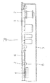
【図6】 従来の自動ドア用制御装置の断面図である。
【符号の説明】
1・・・・・・基板
2・・・・・・パネル
3・・・・・・カバー
4・・・・・・パワー半導体
5・・・・・・電子部品
6・・・・・・放熱面
7・・・・・・スポットナット
8・・・・・・ネジ
10、20・・・自動ドア用制御装置
11・・・・・・操作スイッチ
12・・・・・・ボリューム
13・・・・・・孔
15・・・・・・放熱板
16・・・・・・フレーム
17・・・・・・カラー
18・・・・・・押さえ板
19・・・・・・ハーネス[0001]
[Industrial application fields]
The present invention relates to cooling of electronic components in an automatic door control device.
[0002]
[Prior art]
In recent years, a DC motor has been used as a drive source for opening and closing an automatic door. A power semiconductor is frequently used in a drive circuit for controlling the motor. In addition, various measures are taken to reduce the loss of the semiconductor as the output of the drive circuit increases.
[0003]
A conventional automatic
[0004]
With such a configuration, the heat generated in the
[0005]
[Problems to be solved by the invention]
However, the conventional automatic door control device requires an expensive heat sink to cool the power semiconductor, and it takes time to attach the heat sink to the substrate and the power semiconductor to the heat sink. There was a problem that the depth of the apparatus became large.
[0006]
Further, it is necessary to attach the operation switch and the volume to the panel and to connect the lead wire from the switch to the substrate, so that there is a problem that the work time is increased and the material cost is increased.
[0007]
The present invention has been made in view of such circumstances, and it is an object of the present invention to provide an automatic door control device that is inexpensive and thin.
[0008]
[Means for Solving the Problems]
In order to solve the above-described problems, in an automatic door control device incorporating a drive circuit, a large number of electronic components including a power semiconductor, a substrate on which the electronic component is mounted, and a front surface of the substrate are arranged. Both ends of a metal leaf spring that is formed of a metal panel that holds the back surface and a cover that covers the back surface and side surface of the substrate, and is bent substantially flatly on the back surface of the panel. Fixing the part,
The heat sink can be omitted by bringing the metal leaf spring into surface contact with the heat dissipation surface of the power semiconductor and cooling the power semiconductor by the spring material and the panel , thereby reducing the price of the control device. The problem is solved.
[ 0009 ]
[Action]
Since the metal panel is in surface contact with the heat dissipation surface of the power semiconductor, the heat generated inside the power semiconductor is conducted to the panel and radiated at this location. As a result, the temperature of the power semiconductor is lowered, so that damage to the semiconductor due to the temperature rise can be prevented.
[ 0010 ]
According to the second aspect of the present invention, by directly mounting the operation switch, the volume and the like on the substrate, the connection between the switch and the volume and the substrate becomes unnecessary.
[ 0011 ]
【Example】
Hereinafter, an automatic door control device according to an embodiment of the present invention will be described with reference to the embodiment shown in the drawings. FIG. 1 is an exploded perspective view of the automatic door control device according to the embodiment of the present invention. 2 is a cross-sectional view of an automatic door control device according to an embodiment of the present invention, and FIG. 3 is a cross-sectional view of an automatic door control device according to a second embodiment of the present invention. 4 is a cross-sectional view of an automatic door control device according to a third embodiment of the present invention, and FIG. 5 is a cross-sectional view of an automatic door control device according to a fourth embodiment of the present invention.
[ 0012 ]
The main symbols of the automatic
[ 0013 ]
[ 0014 ]
[ 0015 ]
Reference numeral 3 denotes a cover. The back 3 and the side of the
[ 0016 ]
In such a configuration, the heat dissipating surface of the
[ 0017 ]
Thus, the
[ 0018 ]
As described above, the automatic
[ 0019 ]
Further, according to
[ 0020 ]
When there is a component taller than the width of the
[ 0021 ]
Further, as another method in the case where there is a tall
[ 0022 ]
Furthermore, when a component taller than the
[ 0023 ]
In any of the embodiments, the panel is flat. However, a panel obtained by bending the panel into an L shape or a U shape may be used. By doing so, the cooling efficiency of the
[ 0024 ]
And the fastening of the board |
[ 0025 ]
Further, in the embodiment, the
[ 0026 ]
When two or more types of power semiconductors having different thicknesses are used, a metal plate having a difference in thickness may be interposed between the thinner semiconductors and fastened.
[ 0027 ]
The cover 3 may be made of an inexpensive material such as resin, and if there is a risk of electric shock due to a short circuit, the cover 3 may be grounded by connecting a ground wire to the panel.
[ 0028 ]
In addition, the structure demonstrated by the said Example shows an example of this invention, and does not limit this invention. It goes without saying that the present invention includes a wide variety of modifications that do not depart from the spirit of the present invention.
[ 0029 ]
【The invention's effect】
As described above, the control device for an automatic door of the present invention can dissipate heat generated in the power semiconductor by the panel by bringing the heat semiconductor heat dissipation surface into surface contact with the panel made of metal material. It becomes unnecessary, can reduce parts and man-hours, and can reduce the thickness of the control device.
[ 0030 ]
According to the second aspect of the present invention, by mounting a switch or the like on the substrate, it is possible to reduce parts and man-hours and to reduce the thickness of the control device.
[ 0031 ]
[Brief description of the drawings]
FIG. 1 is an exploded perspective view of a control device for an automatic door according to an embodiment of the present invention.
FIG. 2 is a cross-sectional view of an automatic door control device according to an embodiment of the present invention.
FIG. 3 is a cross-sectional view of an automatic door control device according to a second embodiment of the present invention.
FIG. 4 is a cross-sectional view of an automatic door control device according to a third embodiment of the present invention.
FIG. 5 is a cross-sectional view of an automatic door control device according to a fourth embodiment of the present invention.
FIG. 6 is a cross-sectional view of a conventional automatic door control device.
[Explanation of symbols]
1 ....
Claims (1)
パワー半導体を含む多数の電子部品と、
この電子部品を実装した基板と、
この基板の前面に配し、この基板を保持する金属材製のパネルと、
前記基板の裏面及び側面を覆っているカバーとから構成され、
前記パネルの裏面に、略山形で頂上部がフラットに曲げ加工された金属製板バネの両端部を固定し、
この金属製板バネを前記パワー半導体の放熱面に面接触させて、
前記板バネ及び前記パネルにより、前記パワー半導体を冷却することを特徴とする自動ドア用制御装置。In the automatic door control device with built-in drive circuit,
Many electronic components including power semiconductors,
A board on which this electronic component is mounted;
Arranged on the front of this board, a metal panel that holds this board,
A cover covering the back and side surfaces of the substrate;
At the back of the panel, fix both ends of a metal leaf spring that has a substantially chevron shape and the top is bent flat,
This metal leaf spring is brought into surface contact with the heat dissipation surface of the power semiconductor,
The automatic door control device, wherein the power semiconductor is cooled by the leaf spring and the panel.
Priority Applications (1)
| Application Number | Priority Date | Filing Date | Title |
|---|---|---|---|
| JP32032097A JP3803772B2 (en) | 1997-11-05 | 1997-11-05 | Automatic door control device |
Applications Claiming Priority (1)
| Application Number | Priority Date | Filing Date | Title |
|---|---|---|---|
| JP32032097A JP3803772B2 (en) | 1997-11-05 | 1997-11-05 | Automatic door control device |
Publications (2)
| Publication Number | Publication Date |
|---|---|
| JPH11141230A JPH11141230A (en) | 1999-05-25 |
| JP3803772B2 true JP3803772B2 (en) | 2006-08-02 |
Family
ID=18120179
Family Applications (1)
| Application Number | Title | Priority Date | Filing Date |
|---|---|---|---|
| JP32032097A Expired - Fee Related JP3803772B2 (en) | 1997-11-05 | 1997-11-05 | Automatic door control device |
Country Status (1)
| Country | Link |
|---|---|
| JP (1) | JP3803772B2 (en) |
-
1997
- 1997-11-05 JP JP32032097A patent/JP3803772B2/en not_active Expired - Fee Related
Also Published As
| Publication number | Publication date |
|---|---|
| JPH11141230A (en) | 1999-05-25 |
Similar Documents
| Publication | Publication Date | Title |
|---|---|---|
| JP4357762B2 (en) | Vehicle power distributor | |
| KR100774060B1 (en) | Electronic circuit apparatus | |
| JP4218184B2 (en) | Mounting structure of semiconductor device | |
| US20020195262A1 (en) | Plastic frame for the mounting of an electronic heavy-current control unit | |
| JP2002217343A (en) | Electronic device | |
| EP3403903B1 (en) | Integral-type electric power steering device | |
| WO2017038419A1 (en) | Circuit structure and electrical junction box | |
| JP3803772B2 (en) | Automatic door control device | |
| JP2002324989A (en) | Heat radiating structure for printed circuit board | |
| JP2001177280A (en) | Casing for electric device | |
| JP2022010604A (en) | Electronic apparatus | |
| JPH09213852A (en) | Heat dissipating structure of heating electronic component | |
| WO2001062057A1 (en) | Heat sink with an integrated component clamping device | |
| JP3411512B2 (en) | Electronics | |
| JP3008810B2 (en) | Heat dissipation structure of electrical junction box with built-in electronic circuit unit | |
| CN214125809U (en) | Heat dissipation device and electric tool with same | |
| KR200256593Y1 (en) | Structure for heat sink of the power device | |
| JP3621602B2 (en) | Heat dissipation device for heat generating electronic components | |
| JPH0234992A (en) | Heat dissipation structure of heating element | |
| JP2924286B2 (en) | Electronic circuit device | |
| JP2000292050A (en) | Refrigerator | |
| JPH1093271A (en) | Heat-dissipating and fixing methods of power device package | |
| KR200146570Y1 (en) | Coiled cooling plate for ics | |
| JPH0611389U (en) | Mounting structure for electronic components | |
| JPH0539648Y2 (en) |
Legal Events
| Date | Code | Title | Description |
|---|---|---|---|
| A621 | Written request for application examination |
Free format text: JAPANESE INTERMEDIATE CODE: A621 Effective date: 20041028 |
|
| A977 | Report on retrieval |
Free format text: JAPANESE INTERMEDIATE CODE: A971007 Effective date: 20060116 |
|
| A131 | Notification of reasons for refusal |
Free format text: JAPANESE INTERMEDIATE CODE: A131 Effective date: 20060118 |
|
| A521 | Written amendment |
Free format text: JAPANESE INTERMEDIATE CODE: A523 Effective date: 20060317 |
|
| TRDD | Decision of grant or rejection written | ||
| A01 | Written decision to grant a patent or to grant a registration (utility model) |
Free format text: JAPANESE INTERMEDIATE CODE: A01 Effective date: 20060411 |
|
| A61 | First payment of annual fees (during grant procedure) |
Free format text: JAPANESE INTERMEDIATE CODE: A61 Effective date: 20060418 |
|
| R150 | Certificate of patent (=grant) or registration of utility model |
Free format text: JAPANESE INTERMEDIATE CODE: R150 |
|
| LAPS | Cancellation because of no payment of annual fees |