JP3778128B2 - Manufacturing method of semiconductor device having membrane - Google Patents
Manufacturing method of semiconductor device having membrane Download PDFInfo
- Publication number
- JP3778128B2 JP3778128B2 JP2002138549A JP2002138549A JP3778128B2 JP 3778128 B2 JP3778128 B2 JP 3778128B2 JP 2002138549 A JP2002138549 A JP 2002138549A JP 2002138549 A JP2002138549 A JP 2002138549A JP 3778128 B2 JP3778128 B2 JP 3778128B2
- Authority
- JP
- Japan
- Prior art keywords
- film
- membrane
- etching
- cavity
- forming
- Prior art date
- Legal status (The legal status is an assumption and is not a legal conclusion. Google has not performed a legal analysis and makes no representation as to the accuracy of the status listed.)
- Expired - Fee Related
Links
Images


Classifications
-
- B—PERFORMING OPERATIONS; TRANSPORTING
- B81—MICROSTRUCTURAL TECHNOLOGY
- B81C—PROCESSES OR APPARATUS SPECIALLY ADAPTED FOR THE MANUFACTURE OR TREATMENT OF MICROSTRUCTURAL DEVICES OR SYSTEMS
- B81C1/00—Manufacture or treatment of devices or systems in or on a substrate
- B81C1/00015—Manufacture or treatment of devices or systems in or on a substrate for manufacturing microsystems
- B81C1/00023—Manufacture or treatment of devices or systems in or on a substrate for manufacturing microsystems without movable or flexible elements
- B81C1/00047—Cavities
-
- G—PHYSICS
- G01—MEASURING; TESTING
- G01L—MEASURING FORCE, STRESS, TORQUE, WORK, MECHANICAL POWER, MECHANICAL EFFICIENCY, OR FLUID PRESSURE
- G01L9/00—Measuring steady of quasi-steady pressure of fluid or fluent solid material by electric or magnetic pressure-sensitive elements; Transmitting or indicating the displacement of mechanical pressure-sensitive elements, used to measure the steady or quasi-steady pressure of a fluid or fluent solid material, by electric or magnetic means
- G01L9/0041—Transmitting or indicating the displacement of flexible diaphragms
- G01L9/0042—Constructional details associated with semiconductive diaphragm sensors, e.g. etching, or constructional details of non-semiconductive diaphragms
-
- G—PHYSICS
- G01—MEASURING; TESTING
- G01P—MEASURING LINEAR OR ANGULAR SPEED, ACCELERATION, DECELERATION, OR SHOCK; INDICATING PRESENCE, ABSENCE, OR DIRECTION, OF MOVEMENT
- G01P15/00—Measuring acceleration; Measuring deceleration; Measuring shock, i.e. sudden change of acceleration
- G01P15/02—Measuring acceleration; Measuring deceleration; Measuring shock, i.e. sudden change of acceleration by making use of inertia forces using solid seismic masses
- G01P15/08—Measuring acceleration; Measuring deceleration; Measuring shock, i.e. sudden change of acceleration by making use of inertia forces using solid seismic masses with conversion into electric or magnetic values
- G01P15/0802—Details
-
- G—PHYSICS
- G01—MEASURING; TESTING
- G01P—MEASURING LINEAR OR ANGULAR SPEED, ACCELERATION, DECELERATION, OR SHOCK; INDICATING PRESENCE, ABSENCE, OR DIRECTION, OF MOVEMENT
- G01P15/00—Measuring acceleration; Measuring deceleration; Measuring shock, i.e. sudden change of acceleration
- G01P15/02—Measuring acceleration; Measuring deceleration; Measuring shock, i.e. sudden change of acceleration by making use of inertia forces using solid seismic masses
- G01P15/08—Measuring acceleration; Measuring deceleration; Measuring shock, i.e. sudden change of acceleration by making use of inertia forces using solid seismic masses with conversion into electric or magnetic values
- G01P15/125—Measuring acceleration; Measuring deceleration; Measuring shock, i.e. sudden change of acceleration by making use of inertia forces using solid seismic masses with conversion into electric or magnetic values by capacitive pick-up
-
- B—PERFORMING OPERATIONS; TRANSPORTING
- B81—MICROSTRUCTURAL TECHNOLOGY
- B81B—MICROSTRUCTURAL DEVICES OR SYSTEMS, e.g. MICROMECHANICAL DEVICES
- B81B2201/00—Specific applications of microelectromechanical systems
- B81B2201/02—Sensors
- B81B2201/0264—Pressure sensors
-
- B—PERFORMING OPERATIONS; TRANSPORTING
- B81—MICROSTRUCTURAL TECHNOLOGY
- B81B—MICROSTRUCTURAL DEVICES OR SYSTEMS, e.g. MICROMECHANICAL DEVICES
- B81B2203/00—Basic microelectromechanical structures
- B81B2203/01—Suspended structures, i.e. structures allowing a movement
- B81B2203/0127—Diaphragms, i.e. structures separating two media that can control the passage from one medium to another; Membranes, i.e. diaphragms with filtering function
-
- B—PERFORMING OPERATIONS; TRANSPORTING
- B81—MICROSTRUCTURAL TECHNOLOGY
- B81C—PROCESSES OR APPARATUS SPECIALLY ADAPTED FOR THE MANUFACTURE OR TREATMENT OF MICROSTRUCTURAL DEVICES OR SYSTEMS
- B81C2203/00—Forming microstructural systems
- B81C2203/01—Packaging MEMS
- B81C2203/0145—Hermetically sealing an opening in the lid
-
- B—PERFORMING OPERATIONS; TRANSPORTING
- B81—MICROSTRUCTURAL TECHNOLOGY
- B81C—PROCESSES OR APPARATUS SPECIALLY ADAPTED FOR THE MANUFACTURE OR TREATMENT OF MICROSTRUCTURAL DEVICES OR SYSTEMS
- B81C2203/00—Forming microstructural systems
- B81C2203/01—Packaging MEMS
- B81C2203/0172—Seals
- B81C2203/019—Seals characterised by the material or arrangement of seals between parts
Description
【0001】
【発明の属する技術分野】
本発明は、表面加工式のメンブレンを有する半導体装置の製造方法に関する。
【0002】
【従来の技術】
この種の半導体装置は、半導体基板の表面側に形成された空洞部と、半導体基板の表面側にて空洞部を覆って気密に封止するメンブレンとを有する。そして、これら空洞部およびメンブレンともに、半導体基板の表面側からの成膜やエッチング等によって形成されるものである。
【0003】
このようなものとしては、例えば、シリコン表面加工式圧力センサが知られている。この圧力センサは、シリコンウェハの歪みゲージ・電極等を形成する面から所望の部位をエッチングして除去することによって、メンブレンとしてのダイアフラムならびに空洞部としての圧力基準室を形成する方式のものである。
【0004】
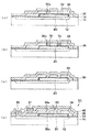
このようなシリコン表面加工式圧力センサとしては、特表2001−504994号公報に記載のものが提案されている。この圧力センサを製造するための従来の一般的な製造方法を図5に示す。
【0005】
まず、図5(a)に示すように、シリコン基板500の一面に、P型不純物拡散層(P−well)等からなる下部電極510を形成した後、その上に酸化シリコン膜520を形成する。
【0006】
次に、図5(b)に示すように、不純物がドープされた多結晶シリコン膜530を成膜し、所望の形状に加工するとともに、この多結晶シリコン膜530においてはその表面から酸化シリコン膜520まで到達するエッチングホール540を形成する。
【0007】
次に、図5(c)に示すように、センサ部以外をレジスト550等で保護した後、上記多結晶シリコン530のエッチングホール540を通して、その下の酸化シリコン膜520をHF(フッ酸)等を用いて、エッチングし除去する。それにより、酸化シリコン膜520が除去された部分において、圧力基準室560および多結晶シリコン膜530からなるメンブレンが形成される。
【0008】
次に、図5(d)に示すように、レジスト550を除去した後、酸化シリコン膜570を成膜して、多結晶シリコン膜530のエッチングホール540を塞ぐことにより、圧力基準室560を気密に封止する。
【0009】
次に、図5(e)に示すように、下部電極510や多結晶シリコン膜530の取り出し部である電極580をAl等により形成するとともに、窒化シリコン等からなる保護膜590を形成する。
【0010】
次に、図5(f)に示すように、上記メンブレンにおける変形部505を規定するため、メンブレンにおける所望の位置にて保護膜590および酸化シリコン膜570を除去する。この除去された部分は周囲に比べて薄く変形しやすくなることから、この除去された部分の内周側が変形部505として規定される。
【0011】
ここで、変形部505を規定する理由は、犠牲層としての酸化シリコン膜520をエッチング除去して空洞部としての圧力基準室560を形成する際に、このエッチングのストッパとなる部分が無いため、メンブレンのサイズを正確に所望のサイズにすることが困難なことによる。
【0012】
このような圧力センサは、平行平板式の容量検出型の圧力センサとして機能する。すなわち、上部電極である多結晶シリコン膜530と下部電極510との間にコンデンサが形成されており、圧力の印加によって変形部505が変位するとこれら上下電極510、530間の距離が変化し、容量も変化する。この容量変化を検出することで圧力検出がなされる。
【0013】
【発明が解決しようとする課題】
ところで、上記圧力センサに代表されるような表面加工式の半導体装置に対して、裏面加工式の半導体装置が知られている。例えば、シリコン裏面加工式の圧力センサは、シリコンウェハの歪みゲージ・電極等を形成する面とは反対の面から所望の部位をエッチングして除去することによって、メンブレンとしてのダイアフラムを形成した後、当該反対の面とガラス台座とを接合して空洞部としての圧力基準室を形成するものである。
【0014】
このような裏面加工式と表面加工式とを比較した場合、シリコン基板そのものをエッチング除去して圧力基準室を形成する裏面加工式に比べ、犠牲層をエッチング除去して圧力基準室を形成する表面加工式では、圧力基準室の容積がおおよそ2桁以上小さい場合が多い。
【0015】
そのため、表面加工式においては、圧力基準室のわずかな内圧変動がセンサ特性に敏感に影響してくることから、いっそう高い気密性が要求されるようになっている。
【0016】
ここで、上記図5において、圧力基準室560の気密性は、(d)の工程におけるエッチングホール540の封止膜である酸化シリコン膜570の成膜方法に大きく依存する。
【0017】
半導体プロセスに整合する成膜方法としては、従来よりCVD法(化学的気相成長法)やPVD(物理的気相成長法)といった方法が一般的に行われているが、それぞれに以下に示すような問題があり、高い信頼性を得ることは困難である。
【0018】
まず、減圧CVD法で酸化シリコン膜570を形成する場合、成膜材料がエッチングホール540から圧力基準室560内へ回り込む。そのため、酸化シリコン膜570が圧力基準室560内にも成膜され、メンブレンの厚さが変化し、メンブレンの変形に支障をきたす。最悪の場合は、酸化シリコン膜570が支柱となってメンブレンの変形を拘束する場合も想定される。
【0019】
また、常圧CVD法で酸化シリコン膜570を形成する場合、圧力基準室560内の圧力が大気圧になるので、環境温度で圧力基準室560内の圧力が、ボイルシャルルの法則により変動する。それにより、上記減圧CVD法の場合と同様、メンブレンの変形に支障をきたす。特に、検出圧力が低い場合には、センサ出力の温度特性が大きく調整が困難となる。
【0020】
また、P−CVD(プラズマCVD)法で酸化シリコン膜570を形成する場合、酸化シリコン膜570の成膜過程から、エッチングホール540の開口部等に存在する段差部にてスリット575が発生する(図5(d)参照)。このスリット575はクラックや割れ目等のことであり、それにより、酸化シリコン膜570のシール長が短くなるなど、気密信頼性を確保することが困難となる。
【0021】
また、電子ビーム蒸着、スパッタリング等のPVD法で酸化シリコン膜570を形成する場合、上記P−CVD法の場合と同様、段差部におけるステップカバレージが悪く、酸化シリコン膜570のシール長が短くなるなど、気密信頼性を確保することが困難となる。
【0022】
このように、従来のエッチングホールの封止膜の成膜方法においては、その成膜過程における封止膜の圧力基準室(空洞部)内への回り込みや圧力基準室内の圧力変動によってメンブレン特性が確保できなかったり、不十分なカバレージによって圧力基準室の気密信頼性が不十分であったりするという問題が生じてしまう。
【0023】
なお、このような問題は、上記表面加工式の圧力センサ以外にも、半導体基板の表面側に形成された空洞部をメンブレンにて気密に封止してなる表面加工式の半導体装置に共通の問題と考えられる。
【0024】
例えば、メンブレンに検出部を形成してなるサーモパイル式の赤外線センサでは、空洞部内を高真空として、メンブレンの熱絶縁性を確保することによって、検出精度を高めている。この場合に、空洞部の気密信頼性が悪いとメンブレンの熱絶縁特性が悪化し、問題になる。
【0025】
そこで、本発明は上記問題に鑑み、半導体基板の表面側に形成された空洞部をメンブレンにて気密に封止してなる表面加工式の半導体装置において、メンブレン特性を確保しつつ、空洞部における信頼性の高い気密封止を行うことができるようにすることを目的とする。
【0026】
【課題を解決するための手段】
上記目的を達成するため、請求項1に記載の発明では、半導体基板(10)と、半導体基板の一面側に形成された空洞部(20)と、半導体基板の一面側にて空洞部を覆って気密に封止するメンブレン(30)とを有する半導体装置の製造方法であって、半導体基板の一面上における空洞部を形成する予定の部位に犠牲層(60)を形成する工程と、犠牲層の表面にエッチング用メンブレン保護膜(32)を形成する工程と、犠牲層を覆うように半導体基板の一面上に、メンブレンとなる第1の膜(34)を形成し、その厚み方向に貫通孔(34a)を有した形状にパターニングする工程と、第1の膜の上に貫通孔を塞ぐように、加熱時に粘性流動可能な第2の膜(36)を形成する工程と、貫通孔に対応する部位にて第2の膜の表面からエッチング用メンブレン保護膜を介して犠牲層に到達するエッチングホール(70)を形成する工程と、エッチング用メンブレン保護膜により第1の膜が保護されるようにエッチングホールを介して犠牲層をエッチング除去することにより空洞部を形成する工程と、第2の膜を加熱して粘性流動させることによりエッチングホールを塞ぐ工程と、を備えることを特徴とする。
また、請求項2に記載の発明では、半導体基板(10)と、半導体基板の一面側に形成された空洞部(20)と、半導体基板の一面側にて空洞部を覆って気密に封止するメンブレン(30)とを有する半導体装置の製造方法であって、半導体基板の一面上における空洞部を形成する予定の部位に犠牲層(60)を形成する工程と、犠牲層を覆うように半導体基板の一面上に、メンブレンとなる第1の膜(34)を形成する工程と、第1の膜の上に、加熱時に粘性流動可能な第2の膜(36)を形成する工程と、第2の膜の表面から第1の膜を介して犠牲層に到達するエッチングホール(70)を形成する工程と、エッチングホールを介して犠牲層をエッチング除去することにより空洞部を形成する工程と、第2の膜を加熱して粘性流動させることによりエッチングホールを塞ぐ工程と、を備えることを特徴とする。
【0027】
それによれば、加熱時に粘性流動可能な第2の膜がエッチングホールの封止膜として機能する。この第2の膜によるエッチングホールの封止は、第2の膜の成膜過程にて行われるものではなく、第2の膜を成膜した後、第2の膜を加熱して粘性流動させることにより行われる。
【0028】
そのため、エッチングホールの大きさや数を適切に制御してやれば、従来のように、封止膜の成膜過程にて封止膜がエッチングホールから空洞部内へ回り込むことは無くなる。また、成膜された第2の膜において従来のようなスリットが発生していたとしても、第2の膜が粘性流動することによってスリットを無くすことができる。
【0029】
また、従来の封止膜の形成方法では、空洞部内の圧力は、封止膜を成膜する際の圧力や雰囲気に律速され、これら成膜圧力や成膜雰囲気で決まってしまう。その点、本発明によれば、空洞部内の圧力は、第2の膜を加熱する際の圧力や雰囲気によって決まる。
【0030】
そして、この加熱時の圧力や雰囲気は任意のものにできるため、空洞部内の圧力を決める自由度が向上する。そのため、メンブレンの変形や熱絶縁性等のメンブレン特性を確保するために、空洞部内の圧力を所望の値にすることが自由にできる。
【0031】
このように、本発明によれば、表面加工型のメンブレンを有する半導体装置において、メンブレン特性を確保しつつ、空洞部における信頼性の高い気密封止を行うことができる。
【0036】
なお、上記各手段の括弧内の符号は、後述する実施形態に記載の具体的手段との対応関係を示す一例である。
【0037】
【発明の実施の形態】
以下、本発明を図に示す実施形態について説明する。図1は本発明の実施形態に係る半導体装置としての圧力センサS1の概略断面構成を示す図である。
【0038】
この圧力センサS1は、大きくは、半導体基板10の一面側に形成された空洞部20と、半導体基板10の一面側にて空洞部20を覆って気密に封止するメンブレン30とを有する。ここで、メンブレン30は圧力の印加によってたわみ変形するダイアフラムとして作用するものである。
【0039】
上記半導体基板としてのシリコン基板10の一面には、下部電極として働く低抵抗層12が形成されている。本例では、低抵抗層12は、P型ウェル層やN型ウェル層等のシリコン基板10とは導電型の異なる不純物拡散層からなる。
【0040】
下部電極12すなわち低抵抗層12の上には酸化シリコン膜14が形成されており、シリコン基板10の一面全体を覆っている。この酸化シリコン膜14を以下、第1の酸化シリコン膜14という。
【0041】
第1の酸化シリコン膜14は、後述する多結晶シリコンもしくはアモルファスシリコンからなる犠牲層をエッチングする時にシリコン基板10を保護するために働くエッチング用基板保護膜である。このエッチング用基板保護膜14すなわち第1の酸化シリコン膜14は熱酸化、スパッタリング、蒸着等により成膜することができる。
【0042】
第1の酸化シリコン膜14の上には、上記空洞部20を介して酸化シリコン膜32が形成されている。この酸化シリコン膜32を以下、第2の酸化シリコン膜32という。この空洞部20の平面形状は例えば円形とすることができる。
【0043】
また、第2の酸化シリコン膜32の上には、第2の酸化シリコン膜32を覆うように、多結晶シリコン膜34が形成されている。この多結晶シリコン膜34はメンブレン30における上部電極として働くものである。この上部電極34すなわち多結晶シリコン膜34は、CVDやスパッタリング等により成膜することができる。
【0044】
ここで、上記第2の酸化シリコン膜32は、後述する多結晶シリコンもしくはアモルファスシリコンからなる犠牲層をエッチングする時に、メンブレン30における多結晶シリコン膜34を保護するために働くエッチング用メンブレン保護膜である。このエッチング用メンブレン保護膜32すなわち第2の酸化シリコン膜32は熱酸化、スパッタリング、蒸着等により成膜することができる。
【0045】
ここで、第2の酸化シリコン膜32および多結晶シリコン膜34には、空洞部20側の内面から外面まで貫通する、すなわち厚み方向に貫通する貫通孔32a、34aが形成されている。第2の酸化シリコン膜32の貫通孔32aと多結晶シリコン膜34の貫通孔34aとは一致している。
【0046】
上部電極すなわち多結晶シリコン膜34の上には、多結晶シリコン膜34の貫通孔34aを塞ぐように第3の酸化シリコン膜36が形成されている。この第3の酸化シリコン膜36は、加熱時に粘性流動可能な膜であり、例えばリンがドープされた酸化シリコンであるPSGや、ボロンとリンがドープされた酸化シリコンであるBPSG等からなる。
【0047】
こうして、空洞部20の直上に位置する薄膜部32、34、36さらには後述する保護膜40によって、メンブレン30が構成されている。そして、空洞部20はメンブレン30によって気密に封止され、真空雰囲気など一定の内圧に維持された圧力基準室として構成されている。
【0048】
ここで、メンブレン30のうち多結晶シリコン膜34が、空洞部20側に位置するとともに厚み方向に貫通する貫通孔34aを有する第1の膜として構成され、第3の酸化シリコン膜36が、加熱時に粘性流動可能な膜であって貫通孔34aを塞ぐように多結晶シリコン膜34を覆う第2の膜として構成される。
【0049】
また、図1に示すように、第3の酸化シリコン膜36の上には、CVD、スパッタリングや蒸着等により成膜された窒化シリコン等からなる保護膜40が形成されている。この保護膜40によって、シリコン基板10の一面側の構成要素が被覆され保護される。
【0050】
また、シリコン基板10の一面上における空洞部20の周囲には、下部電極としての低抵抗層12、上部電極としての多結晶シリコン膜34をそれぞれ外部に接続するための取り出し電極50、51が設けられている。これら取り出し電極50、51は、蒸着等により形成されたアルミニウム等の金属等からなる。
【0051】
下部電極用の取り出し電極50は、保護膜40の表面から低抵抗層12まで貫通するコンタクトホールに形成され、低抵抗層12と電気的に接続されている。また、上部電極用の取り出し電極51は、保護膜40の表面から多結晶シリコン膜34まで貫通するコンタクトホールに形成され、多結晶シリコン膜34と電気的に接続されている。
【0052】
このような圧力センサS1においては、上部電極である多結晶シリコン膜34と下部電極である低抵抗層12との間にコンデンサが形成されており、このコンデンサの容量値を検出可能となっている。また、メンブレン30は圧力を受圧するとたわんで変位し、この変位によって、多結晶シリコン膜34と低抵抗層12との間の距離が変化するようになっている。
【0053】
したがって、本圧力センサS1は平行平板式の容量検出型の圧力センサとして機能し、圧力の印加によってメンブレン30が変位し、この変位に伴う上下電極12、34間の容量変化に基づいて印加圧力を検出できるようになっている。
【0054】
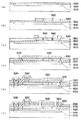
次に、上記構成を有する圧力センサS1の製造方法について述べる。図2、図3は図1に示す圧力センサS1の製造方法を示す工程図であり、図1に対応した断面にて示してある。
【0055】
[図2(a)の工程]
シリコン基板10の一面に、イオン注入や拡散等の半導体プロセス技術を用いて不純物拡散層からなる低抵抗層12を形成する。その上に、熱酸化、スパッタリング、蒸着等により第1の酸化シリコン膜14を成膜する。
【0056】
[図2(b)の工程]
次に、シリコン基板10の一面上における空洞部20を形成する予定の部位に犠牲層60を形成する。本例では、多結晶シリコンからなる膜をCVD、スパッタリング、蒸着等により成膜するとともに、フォトリソグラフ技術を用いて空洞部20の形状(例えば平面円形)にパターニングすることにより、犠牲層60を形成する。
【0057】
続いて、犠牲層60に対して熱酸化等の酸化処理を施すことにより、犠牲層60の表面に第2の酸化シリコン膜32を形成する。この状態が図2(b)に示されている。なお、本工程において、犠牲層60は多結晶シリコンに代えてアモルファスシリコンからなるものとしても良い。また、第2のシリコン酸化膜32はスパッタリング、蒸着等により成膜しても良い。
【0058】
[図2(c)の工程]
次に、犠牲層60を覆うようにシリコン基板10の一面上に、メンブレン30の第1の膜となる多結晶シリコン膜34を形成する。具体的には、多結晶シリコンをCVDやスパッタリング等により成膜するとともに、フォトリソグラフ技術を用いて貫通孔34aを有した形状にパターニングすることにより、多結晶シリコン膜34を形成する。
【0059】
[図3(a)の工程]
次に、第1の膜である多結晶シリコン膜34の上に、加熱時に粘性流動可能な第2の膜としての第3の酸化シリコン膜36を形成する。本例では、シリコン基板10の一面の全域上に、CVD等によりPSGまたはBPSGを成膜することにより第3の酸化シリコン膜36を形成する。形成された第3の酸化シリコン膜36により、多結晶シリコン膜34の貫通孔34aは塞がれる。
【0060】
[図3(b)の工程]
次に、ドライエッチング等を行うことにより、第3の酸化シリコン膜36の表面から犠牲層60に到達するエッチングホール70を形成する。このとき、多結晶シリコン膜34の貫通孔34aに対応する部位にてエッチングホール70を形成する。
【0061】
続いて、エッチングホール70を介して犠牲層60をエッチング除去することにより空洞部20を形成する。本例では、多結晶シリコンまたはアモルファスシリコンを選択的にエッチングし、酸化シリコンは実質的にエッチングしないエッチング材料を用いたエッチングにより犠牲層60をエッチングする。
【0062】
具体的なエッチング方法としては、KOHや水酸化テトラメチルアンモニウム(TMAH)を用いたウェットエッチングや、フッ化キセノン(XeF2)を用いたドライエッチング等を採用することができる。
【0063】
なお、本工程では、エッチングホール70を形成するとき、エッチングホール70の内面にて多結晶シリコン膜34が露出しないようにする。もし、多結晶シリコン膜34が露出していると、そこから多結晶シリコン膜34がエッチングされてしまうためである。
【0064】
また、後工程で行うエッチングホール70の封止のためには、エッチングホール70の穴径については小さい方が、また穴数については少ない方が望ましいが、エッチング材料の導入のしやすさに対してトレードオフの関係になるので、適切な穴径、穴数を選択することが肝要である。
【0065】
[図3(c)の工程]
次に、第2の膜である第3の酸化シリコン膜36を加熱して粘性流動(リフロー)させることによりエッチングホール70を塞ぐ。本例におけるPSGやBPSGからなる第3の酸化シリコン膜36の場合、例えば真空中にて900℃程度に加熱することにより、流動が行われる。これにより、内圧が真空であり気密に封止された圧力基準室としての空洞部20が形成される。
【0066】
[図3(d)の工程]
次に、保護膜40を成膜してメンブレン30を形成し、ドライエッチング等によってコンタクトホールを形成した後、各取り出し電極50、51となる導電膜を成膜し、パターニングすることで、取り出し電極50、51を形成する。こうして本圧力センサS1が完成する。
【0067】
なお、本例では、犠牲層60のエッチングは、第1および第2の酸化シリコン膜14、32をエッチングストッパとして終了するため、空洞部20のサイズつまりメンブレン30のサイズは、予め規定されたサイズに正確に形成することができる。そのため、本実施形態では、さらに上記図5に示したような変形部を規定するための加工を行わなくても良い。
【0068】
以上のように、本実施形態によれば、加熱時に粘性流動可能な第3の酸化シリコン膜(第2の膜)36がエッチングホール70の封止膜として機能する。この第3の酸化シリコン膜36によるエッチングホール70の封止は、第3の酸化シリコン膜36の成膜過程にて行われるものではなく、第3の酸化シリコン膜36を成膜した後、これを加熱して粘性流動させることにより行われる。
【0069】
そのため、エッチングホール70の大きさや数を適切に制御してやれば、従来のように、封止膜の成膜過程にて封止膜がエッチングホールから空洞部20内へ回り込むことは無くなる。
【0070】
また、成膜された第3の酸化シリコン膜36において従来のようなスリットが発生していたとしても、第3の酸化シリコン膜36が粘性流動することによってスリットを無くすことができ、封止性能の良い膜となる。
【0071】
また、従来の封止膜の形成方法では、空洞部内の圧力は、封止膜を成膜する際の圧力や雰囲気に律速され、これら成膜圧力や成膜雰囲気で決まってしまう。その点、本実施形態によれば、空洞部20内の圧力は、第3の酸化シリコン膜36を加熱する際の圧力や雰囲気によって決まる。
【0072】
そして、この加熱時の圧力や雰囲気は任意のものにできるため、空洞部20内の圧力を決める自由度が向上する。そのため、メンブレン30の変形や熱絶縁性等のメンブレン特性を確保するために、空洞部20内の圧力を所望の値にすることが自由にできる。本実施形態では、検出圧力に応じて適正な内圧を有する圧力基準室を形成することができる。
【0073】
このように、本実施形態によれば、表面加工型の圧力センサにおいて、メンブレン30の特性を確保しつつ、空洞部20における信頼性の高い気密封止を行うことができる。
【0074】
また、上記図2、図3に示す製造方法では、ディスクリートセンサを例に挙げて記載しているが、一つのチップ内に回路を作り込む集積化圧力センサの場合では、LSIとの整合性に優れるという特徴を有する。
【0075】
これは、例えば、図2(a)〜(c)の工程が、トランジスタ素子等を形成するための不純物拡散層の形成、層間絶縁膜の形成、多結晶シリコン層の形成といった工程を利用して実施できる等の理由による。つまり、本製造方法は、犠牲層エッチング以外は通常のLSI工程を用いて行うことが可能である。
【0076】
特に、EPROM等で2層の多結晶シリコン層を有する工程の場合、この工程において、最低でマスクを1枚追加することにより多結晶シリコン膜34に対して貫通孔34aを形成することができる。
【0077】
[変形例]
なお、本実施形態の圧力センサS1における各部の構成や材質等は上記例に限定されるものではない。例えば、メンブレン30の第2の膜としては、PSGやBPSGからなる第3の酸化シリコン膜36以外のもので代用しても良い。すなわち、当該第2の膜は、製造工程上、当該第2の膜よりも前に形成される部分よりも低い温度で粘性流動可能なものであれば代用可能である。
【0078】
また、下部電極12は、上記した不純物拡散層からなる低抵抗層に代えて、例えば、シリコン基板10の一面に形成された多結晶シリコン膜や金属膜等の他の材料にて構成されたものとしても良い。
【0079】
また、第1の酸化シリコン膜14、第2の酸化シリコン膜32は、多結晶シリコンもしくはアモルファスシリコンからなる犠牲層60をエッチングする時に、それぞれ基板保護膜、メンブレン保護膜として機能するが、このような保護膜としては、犠牲層60のエッチング時にエッチングされないようなもの、例えば窒化シリコン膜等を用いても良い。
【0080】
また、メンブレン30における上部電極34は、上記多結晶シリコン膜34に代えて、同様の機能を有するものとしてアモルファスシリコン膜等を用いても良い。
【0081】
このように、エッチング用基板保護膜14およびエッチング用上部電極保護膜32、さらにはメンブレン30における上部電極34の材質は、犠牲層60の種類によって多様に変化するものであり、それぞれ適宜選択して用いることが必要である。
【0082】
また、第1および第2の酸化シリコン膜14、32などのエッチング用保護膜は、犠牲層60のエッチング時にシリコン基板10やメンブレン30を構成する膜が、実質的にエッチングされない場合には不要である。そのような場合の一例を本実施形態の変形例として図4に示す。
【0083】
図4は、本実施形態の変形例としての製造工程を示す工程図である。ここでは、犠牲層60として窒化シリコンを用いているため、上記第1および第2の酸化シリコン膜12、34などのエッチング用保護膜が不要である。
【0084】
図4(a)に示すように、下部電極12が形成されたシリコン基板10の一面上における空洞部20を形成する予定の部位に窒化シリコンからなる犠牲層60を形成する。そして、犠牲層60を覆うようにメンブレン30の第1の膜である多結晶シリコン膜34を形成する。
【0085】
その後、図4(b)に示すように、多結晶シリコン膜34には貫通孔を形成せずに、多結晶シリコン膜34の上にPSGやBPSGからなる第3の酸化シリコン膜36を形成する。
【0086】
そして、図4(c)に示すように、ドライエッチング等により第3の酸化シリコン膜36の表面から第3の酸化シリコン膜36および多結晶シリコン膜34を貫通して犠牲層60に到達するエッチングホール70を形成する。
【0087】
続いて、熱リン酸等の窒化シリコンを選択的にエッチングするエッチング材料を用いて、エッチングホール70を介して犠牲層60をエッチング除去することにより空洞部20を形成する。
【0088】
その後は、上記同様、第3の酸化シリコン膜36を加熱して粘性流動させることによりエッチングホール70を塞ぎ、保護膜40の形成、取り出し電極50、51の形成等を行い、圧力センサを完成させる。そして、本変形例の圧力センサにおいても、上記図1〜図3に示す例と同様の作用効果が得られる。
【0089】
また、メンブレン30における第1の膜を多結晶シリコン膜34に代えて、例えば窒化シリコン等の絶縁材料からなる膜を空洞部20側に配置し、その上に例えば多結晶シリコンや金属等の導電性材料からなる膜を載せた2層構造としても良い。つまり、第1の膜においてメンブレン(ダイアフラム)の機能と上部電極の機能とを分けた層構成としても良い。
【0090】
(他の実施形態)
なお、上記実施形態では、平行平板式の容量検出型圧力センサを例に挙げているが、上記図1中のメンブレン30を構成する多結晶シリコン膜36に歪みゲージとして働く不純物拡散層を形成する方式としても良い。なお、この場合は下部電極12は不要である。
【0091】
また、本発明は、圧力センサ以外にもサーモパイル式の赤外線センサにも適用することができる。例えば、上記図1において、メンブレン30における第1の膜34を窒化シリコン等で形成し、その上に例えば多結晶シリコン配線とアルミ配線からなる熱電対を形成し、さらにその上に第2の膜36を形成するような構成にて実現可能である。
【0092】
そして、赤外線センサにおいては、空洞部20内を高真空とすることで、メンブレン30の熱絶縁性(断熱性)を良好なものに確保でき、センサ感度を向上させることができる。
【0093】
また、空洞部内に、例えば櫛歯構造をなす可動部を形成することにより、容量式の加速度センサや角速度センサへも活用することができる。空洞部内を高真空にすることにより、外乱の影響を排除した感度の良好なセンサすることができる。
【図面の簡単な説明】
【図1】本発明の実施形態に係る圧力センサの概略断面構成を示す図である。
【図2】図1に示す圧力センサの製造方法を示す工程図である。
【図3】図2に続く製造方法を示す工程図である。
【図4】上記実施形態の変形例としての製造工程を示す工程図である。
【図5】従来の一般的な表面加工式圧力センサの製造方法を示す図である。
【符号の説明】
10…シリコン基板、20…空洞部、30…メンブレン、
34…多結晶シリコン膜、34a…貫通孔、36…第3の酸化シリコン膜、
60…犠牲層、70…エッチングホール。[0001]
BACKGROUND OF THE INVENTION
The present invention relates to a semiconductor device having a surface processed membraneofIt relates to a manufacturing method.
[0002]
[Prior art]
This type of semiconductor device has a cavity formed on the surface side of the semiconductor substrate and a membrane that covers the cavity on the surface side of the semiconductor substrate and hermetically seals. Both the cavity and the membrane are formed by film formation or etching from the surface side of the semiconductor substrate.
[0003]
As such a device, for example, a silicon surface processing type pressure sensor is known. This pressure sensor is of a type that forms a diaphragm as a membrane and a pressure reference chamber as a cavity by etching and removing a desired part from the surface of the silicon wafer on which the strain gauge, electrode, etc. are formed. .
[0004]
As such a silicon surface processing type pressure sensor, a sensor described in JP-T-2001-504994 has been proposed. FIG. 5 shows a conventional general manufacturing method for manufacturing this pressure sensor.
[0005]
First, as shown in FIG. 5A, a
[0006]
Next, as shown in FIG. 5B, a
[0007]
Next, as shown in FIG. 5C, after protecting the portions other than the sensor portion with a
[0008]
Next, as shown in FIG. 5D, after the
[0009]
Next, as shown in FIG. 5E, the
[0010]
Next, as shown in FIG. 5F, the
[0011]
Here, the reason for defining the
[0012]
Such a pressure sensor functions as a parallel plate type capacitance detection type pressure sensor. That is, a capacitor is formed between the
[0013]
[Problems to be solved by the invention]
By the way, a back surface processing type semiconductor device is known with respect to the surface processing type semiconductor device represented by the pressure sensor. For example, after forming a diaphragm as a membrane by etching and removing a desired part from a surface opposite to a surface on which a strain gauge, an electrode and the like of a silicon wafer are formed, a silicon back surface processing type pressure sensor is formed. The opposite surface and the glass pedestal are joined to form a pressure reference chamber as a cavity.
[0014]
When comparing the back surface processing type and the surface processing type, the surface on which the sacrificial layer is removed by etching to form the pressure reference chamber, compared to the back surface processing type in which the silicon substrate itself is removed by etching to form the pressure reference chamber. In the processing type, the volume of the pressure reference chamber is often about two digits or more smaller.
[0015]
For this reason, in the surface processing type, even a slight variation in internal pressure in the pressure reference chamber sensitively affects the sensor characteristics, so that higher airtightness is required.
[0016]
Here, in FIG. 5 described above, the airtightness of the
[0017]
Conventionally, methods such as CVD (Chemical Vapor Deposition) and PVD (Physical Vapor Deposition) have been generally used as film forming methods consistent with semiconductor processes. However, it is difficult to obtain high reliability.
[0018]
First, in the case where the
[0019]
Further, when the
[0020]
Further, when the
[0021]
Further, when the
[0022]
As described above, in the conventional method for forming the sealing film of the etching hole, the membrane characteristics are affected by the wraparound of the sealing film into the pressure reference chamber (cavity) or the pressure fluctuation in the pressure reference chamber during the film forming process. Air pressure reliability of the pressure reference chamber is insufficient due to insufficient coverage or insufficient coverageTsuProblem arises.
[0023]
In addition to the above surface processing type pressure sensor, such a problem is common to the surface processing type semiconductor device in which the cavity formed on the surface side of the semiconductor substrate is hermetically sealed with a membrane. It is considered a problem.
[0024]
For example, in a thermopile infrared sensor in which a detection part is formed on a membrane, the detection accuracy is improved by ensuring the thermal insulation of the membrane by setting the inside of the cavity to a high vacuum. In this case, if the airtight reliability of the cavity is poor, the thermal insulation characteristics of the membrane are deteriorated, which causes a problem.
[0025]
Therefore, in view of the above problems, the present invention provides a surface processing type semiconductor device in which a cavity formed on the surface side of a semiconductor substrate is hermetically sealed with a membrane. It is an object of the present invention to enable highly reliable hermetic sealing.
[0026]
[Means for Solving the Problems]
In order to achieve the above object, according to the first aspect of the present invention, the semiconductor substrate (10), the cavity (20) formed on one surface of the semiconductor substrate, and the cavity on the one surface of the semiconductor substrate are covered. A method of manufacturing a semiconductor device having a membrane (30) that is hermetically sealed, and a step of forming a sacrificial layer (60) at a site where a cavity is to be formed on one surface of a semiconductor substrate;Forming an etching membrane protective film (32) on the surface of the sacrificial layer;A first film (34) serving as a membrane is formed on one surface of the semiconductor substrate so as to cover the sacrificial layer.And patterning into a shape having a through hole (34a) in the thickness directionAnd on the first filmTo close the through holeForming a second film (36) capable of viscous flow during heating;At the part corresponding to the through holeFrom the surface of the second filmThrough the protective membrane for etchingForming an etching hole (70) reaching the sacrificial layer;The first film is protected by the protective membrane for etching.And a step of forming a cavity by etching away the sacrificial layer through the etching hole, and a step of closing the etching hole by heating the second film to cause viscous flow.
According to the second aspect of the present invention, the semiconductor substrate (10), the cavity (20) formed on one side of the semiconductor substrate, and the cavity on the one side of the semiconductor substrate are hermetically sealed. A method of manufacturing a semiconductor device having a membrane (30) for forming a sacrificial layer (60) in a portion where a cavity is to be formed on one surface of a semiconductor substrate, and a semiconductor so as to cover the sacrificial layer Forming a first film (34) to be a membrane on one surface of the substrate, forming a second film (36) capable of viscous flow on heating on the first film, A step of forming an etching hole (70) that reaches the sacrificial layer through the first film from the surface of the film 2, a step of forming a cavity by etching away the sacrificial layer through the etching hole, Heat the second film to make it viscous flow Characterized in that it comprises the the steps of closing the etching hole by the.
[0027]
According to this, the second film capable of viscous flow at the time of heating functions as an etching hole sealing film. The sealing of the etching hole by the second film is not performed in the process of forming the second film, but after the second film is formed, the second film is heated to cause viscous flow. Is done.
[0028]
Therefore, if the size and number of the etching holes are appropriately controlled, the sealing film does not go into the cavity from the etching hole in the process of forming the sealing film as in the prior art. Further, even if a conventional slit occurs in the formed second film, the slit can be eliminated by the viscous flow of the second film.
[0029]
Further, in the conventional method for forming a sealing film, the pressure in the cavity is controlled by the pressure and atmosphere when the sealing film is formed, and is determined by these film forming pressure and film forming atmosphere. In that respect, according to the present invention, the pressure in the cavity is determined by the pressure and atmosphere when the second film is heated.
[0030]
And since the pressure and atmosphere at the time of this heating can be made arbitrary, the freedom degree which determines the pressure in a cavity part improves. Therefore, in order to ensure membrane characteristics such as membrane deformation and thermal insulation, the pressure in the cavity can be freely set to a desired value.
[0031]
As described above, according to the present invention, in a semiconductor device having a surface-processed membrane, it is possible to perform highly reliable hermetic sealing in the cavity while ensuring the membrane characteristics.
[0036]
In addition, the code | symbol in the bracket | parenthesis of each said means is an example which shows a corresponding relationship with the specific means as described in embodiment mentioned later.
[0037]
DETAILED DESCRIPTION OF THE INVENTION
DESCRIPTION OF THE PREFERRED EMBODIMENTS Embodiments shown in the drawings will be described below. FIG. 1 is a diagram showing a schematic cross-sectional configuration of a pressure sensor S1 as a semiconductor device according to an embodiment of the present invention.
[0038]
The pressure sensor S1 roughly includes a
[0039]
A
[0040]
A
[0041]
The first
[0042]
A
[0043]
A
[0044]
Here, the second
[0045]
Here, in the second
[0046]
A third
[0047]
Thus, the
[0048]
Here, the
[0049]
As shown in FIG. 1, a
[0050]
Further, around the
[0051]
The
[0052]
In such a pressure sensor S1, a capacitor is formed between the
[0053]
Therefore, this pressure sensor S1 functions as a parallel plate type capacitance detection type pressure sensor, and the
[0054]
Next, a manufacturing method of the pressure sensor S1 having the above configuration will be described. 2 and 3 are process diagrams showing a manufacturing method of the pressure sensor S1 shown in FIG. 1, and are shown in a cross section corresponding to FIG.
[0055]
[Step of FIG. 2A]
A
[0056]
[Step of FIG. 2B]
Next, a
[0057]
Subsequently, an oxidation treatment such as thermal oxidation is performed on the
[0058]
[Step of FIG. 2C]
Next, a
[0059]
[Step of FIG. 3A]
Next, a third
[0060]
[Step of FIG. 3B]
Next, an
[0061]
Subsequently, the
[0062]
Specific etching methods include wet etching using KOH and tetramethylammonium hydroxide (TMAH), and xenon fluoride (XeF).2The dry etching etc. which used ()) can be employ | adopted.
[0063]
In this step, when the
[0064]
In order to seal the
[0065]
[Step of FIG. 3C]
Next, the third
[0066]
[Step of FIG. 3D]
Next, after forming the
[0067]
In this example, since the etching of the
[0068]
As described above, according to the present embodiment, the third silicon oxide film (second film) 36 capable of viscous flow during heating functions as a sealing film for the
[0069]
Therefore, if the size and the number of the etching holes 70 are appropriately controlled, the sealing film does not go into the
[0070]
Further, even if the conventional
[0071]
Further, in the conventional method for forming a sealing film, the pressure in the cavity is controlled by the pressure and atmosphere when the sealing film is formed, and is determined by these film forming pressure and film forming atmosphere. In this regard, according to the present embodiment, the pressure in the
[0072]
And since the pressure and atmosphere at the time of this heating can be made arbitrary, the freedom degree which determines the pressure in the
[0073]
As described above, according to the present embodiment, in the surface processing type pressure sensor, it is possible to perform highly reliable hermetic sealing in the
[0074]
In the manufacturing method shown in FIGS. 2 and 3, the discrete sensor is described as an example. However, in the case of the integrated pressure sensor in which a circuit is formed in one chip, the compatibility with the LSI is improved. It has the feature of being excellent.
[0075]
This is because, for example, the steps of FIGS. 2A to 2C utilize steps such as formation of an impurity diffusion layer, formation of an interlayer insulating film, formation of a polycrystalline silicon layer for forming a transistor element or the like. The reason is that it can be implemented. That is, this manufacturing method can be performed using a normal LSI process except for the sacrifice layer etching.
[0076]
In particular, in the case of a process having two polycrystalline silicon layers using EPROM or the like, the through
[0077]
[Modification]
In addition, the structure of each part, material, etc. in pressure sensor S1 of this embodiment are not limited to the said example. For example, the second film of the
[0078]
The
[0079]
The first
[0080]
The
[0081]
As described above, the material of the etching
[0082]
Further, the protective films for etching such as the first and second
[0083]
FIG. 4 is a process diagram showing a manufacturing process as a modification of the present embodiment. Here, since silicon nitride is used as the
[0084]
As shown in FIG. 4A, a
[0085]
Thereafter, as shown in FIG. 4B, a third
[0086]
Then, as shown in FIG. 4C, etching that reaches the
[0087]
Subsequently, the
[0088]
Thereafter, as in the above, the third
[0089]
Further, instead of the
[0090]
(Other embodiments)
In the above embodiment, a parallel plate type capacitance detection type pressure sensor is taken as an example, but an impurity diffusion layer serving as a strain gauge is formed in the
[0091]
Further, the present invention can be applied to a thermopile infrared sensor other than the pressure sensor. For example, in FIG. 1, the
[0092]
And in an infrared sensor, by making the inside of the
[0093]
Further, by forming a movable part having a comb-tooth structure, for example, in the hollow part, it can be used for a capacitive acceleration sensor and an angular velocity sensor. By making the inside of the cavity a high vacuum, it is possible to provide a sensor with good sensitivity that eliminates the influence of disturbance.
[Brief description of the drawings]
FIG. 1 is a diagram showing a schematic cross-sectional configuration of a pressure sensor according to an embodiment of the present invention.
2 is a process diagram showing a manufacturing method of the pressure sensor shown in FIG. 1; FIG.
FIG. 3 is a process diagram illustrating the manufacturing method subsequent to FIG. 2;
FIG. 4 is a process diagram showing a manufacturing process as a modification of the embodiment.
FIG. 5 is a diagram showing a conventional method for manufacturing a general surface-processed pressure sensor.
[Explanation of symbols]
10 ... Silicon substrate, 20 ... Cavity, 30 ... Membrane,
34 ... polycrystalline silicon film, 34a ... through hole, 36 ... third silicon oxide film,
60 ... Sacrificial layer, 70 ... Etching hole.
Claims (2)
前記半導体基板の一面上における前記空洞部を形成する予定の部位に犠牲層(60)を形成する工程と、
前記犠牲層の表面にエッチング用メンブレン保護膜(32)を形成する工程と、
前記犠牲層を覆うように前記半導体基板の一面上に、前記メンブレンとなる第1の膜(34)を形成し、その厚み方向に貫通孔(34a)を有した形状にパターニングする工程と、
前記第1の膜の上に前記貫通孔を塞ぐように、加熱時に粘性流動可能な第2の膜(36)を形成する工程と、
前記貫通孔に対応する部位にて前記第2の膜の表面から前記エッチング用メンブレン保護膜を介して前記犠牲層に到達するエッチングホール(70)を形成する工程と、
前記エッチング用メンブレン保護膜により前記第1の膜が保護されるように前記エッチングホールを介して前記犠牲層をエッチング除去することにより前記空洞部を形成する工程と、
前記第2の膜を加熱して粘性流動させることにより前記エッチングホールを塞ぐ工程と、を備えることを特徴とするメンブレンを有する半導体装置の製造方法。A semiconductor substrate (10), a cavity (20) formed on one surface of the semiconductor substrate, and a membrane (30) for hermetically sealing the cavity on the one surface of the semiconductor substrate. A method for manufacturing a semiconductor device, comprising:
Forming a sacrificial layer (60) at a site where the cavity is to be formed on one surface of the semiconductor substrate;
Forming an etching membrane protective film (32) on the surface of the sacrificial layer;
Forming a first film (34) serving as the membrane on one surface of the semiconductor substrate so as to cover the sacrificial layer, and patterning the first film (34a) in a thickness direction thereof ; and
Forming a second film (36) capable of viscous flow at the time of heating so as to block the through hole on the first film;
Forming an etching hole (70) reaching the sacrificial layer from the surface of the second film through the etching membrane protective film at a portion corresponding to the through hole ;
Forming the cavity by etching away the sacrificial layer through the etching hole so that the first film is protected by the membrane protection film for etching ;
A method of manufacturing a semiconductor device having a membrane, comprising: a step of closing the etching hole by heating and viscously flowing the second film.
前記半導体基板の一面上における前記空洞部を形成する予定の部位に犠牲層(60)を形成する工程と、
前記犠牲層を覆うように前記半導体基板の一面上に、前記メンブレンとなる第1の膜(34)を形成する工程と、
前記第1の膜の上に、加熱時に粘性流動可能な第2の膜(36)を形成する工程と、
前記第2の膜の表面から前記第1の膜を介して前記犠牲層に到達するエッチングホール(70)を形成する工程と、
前記エッチングホールを介して前記犠牲層をエッチング除去することにより前記空洞部を形成する工程と、
前記第2の膜を加熱して粘性流動させることにより前記エッチングホールを塞ぐ工程と、を備えることを特徴とするメンブレンを有する半導体装置の製造方法。 A semiconductor substrate (10), a cavity (20) formed on one surface of the semiconductor substrate, and a membrane (30) for hermetically sealing the cavity on the one surface of the semiconductor substrate. A method for manufacturing a semiconductor device, comprising:
Forming a sacrificial layer (60) at a site where the cavity is to be formed on one surface of the semiconductor substrate;
Forming a first film (34) serving as the membrane on one surface of the semiconductor substrate so as to cover the sacrificial layer;
Forming a second film (36) capable of viscous flow on heating on the first film;
Forming an etching hole (70) reaching the sacrificial layer from the surface of the second film through the first film;
Forming the cavity by etching away the sacrificial layer through the etching hole;
Method of manufacturing a semiconductor device having a membrane you characterized by and a step of closing the etching hole by heating the viscous flow of said second film.
Priority Applications (3)
| Application Number | Priority Date | Filing Date | Title |
|---|---|---|---|
| JP2002138549A JP3778128B2 (en) | 2002-05-14 | 2002-05-14 | Manufacturing method of semiconductor device having membrane |
| US10/425,663 US7157781B2 (en) | 2002-05-14 | 2003-04-30 | Enhancement of membrane characteristics in semiconductor device with membrane |
| DE10321482A DE10321482B4 (en) | 2002-05-14 | 2003-05-13 | Improvement of membrane properties of a semiconductor device |
Applications Claiming Priority (1)
| Application Number | Priority Date | Filing Date | Title |
|---|---|---|---|
| JP2002138549A JP3778128B2 (en) | 2002-05-14 | 2002-05-14 | Manufacturing method of semiconductor device having membrane |
Publications (2)
| Publication Number | Publication Date |
|---|---|
| JP2003332587A JP2003332587A (en) | 2003-11-21 |
| JP3778128B2 true JP3778128B2 (en) | 2006-05-24 |
Family
ID=29397584
Family Applications (1)
| Application Number | Title | Priority Date | Filing Date |
|---|---|---|---|
| JP2002138549A Expired - Fee Related JP3778128B2 (en) | 2002-05-14 | 2002-05-14 | Manufacturing method of semiconductor device having membrane |
Country Status (3)
| Country | Link |
|---|---|
| US (1) | US7157781B2 (en) |
| JP (1) | JP3778128B2 (en) |
| DE (1) | DE10321482B4 (en) |
Cited By (1)
| Publication number | Priority date | Publication date | Assignee | Title |
|---|---|---|---|---|
| JP2015129699A (en) * | 2014-01-08 | 2015-07-16 | 三菱電機株式会社 | Method for manufacturing semiconductor device |
Families Citing this family (42)
| Publication number | Priority date | Publication date | Assignee | Title |
|---|---|---|---|---|
| US6936491B2 (en) * | 2003-06-04 | 2005-08-30 | Robert Bosch Gmbh | Method of fabricating microelectromechanical systems and devices having trench isolated contacts |
| DE10352001A1 (en) * | 2003-11-07 | 2005-06-09 | Robert Bosch Gmbh | Micromechanical component with a membrane and method for producing such a component |
| DE102005005551B4 (en) * | 2004-03-03 | 2015-10-01 | Robert Bosch Gmbh | Micromechanical component with a membrane and method for producing such a component |
| JP5009505B2 (en) * | 2004-03-03 | 2012-08-22 | ローベルト ボツシユ ゲゼルシヤフト ミツト ベシユレンクテル ハフツング | Micromachining type component with diaphragm and method for manufacturing such a component |
| JP2005262686A (en) * | 2004-03-18 | 2005-09-29 | Ricoh Co Ltd | Actuator, liquid droplet jet head, ink cartridge, inkjet recorder, micro pump, optical modulation device, and substrate |
| JP4534622B2 (en) * | 2004-06-23 | 2010-09-01 | ソニー株式会社 | Functional element and manufacturing method thereof, fluid discharge head, and printing apparatus |
| JP4617743B2 (en) * | 2004-07-06 | 2011-01-26 | ソニー株式会社 | Functional element, method for manufacturing the same, and fluid discharge head |
| US7820470B2 (en) * | 2005-07-15 | 2010-10-26 | Semiconductor Energy Laboratory Co., Ltd. | Manufacturing method of micro-electro-mechanical device |
| JP4633574B2 (en) * | 2005-08-08 | 2011-02-16 | 三菱電機株式会社 | Thin film structure and manufacturing method thereof |
| US7382515B2 (en) * | 2006-01-18 | 2008-06-03 | Qualcomm Mems Technologies, Inc. | Silicon-rich silicon nitrides as etch stops in MEMS manufacture |
| US7678601B2 (en) * | 2006-01-20 | 2010-03-16 | Texas Instruments Incorporated | Method of forming an acceleration sensor |
| US20070170528A1 (en) | 2006-01-20 | 2007-07-26 | Aaron Partridge | Wafer encapsulated microelectromechanical structure and method of manufacturing same |
| DE102006008584A1 (en) * | 2006-02-24 | 2007-09-06 | Atmel Germany Gmbh | Manufacturing process for integrated piezo components |
| FR2897937B1 (en) * | 2006-02-24 | 2008-05-23 | Commissariat Energie Atomique | PRESSURE SENSOR WITH RESISTIVE GAUGES |
| US8062497B2 (en) * | 2006-03-28 | 2011-11-22 | Imec | Method for forming a hermetically sealed cavity |
| JP2008132583A (en) * | 2006-10-24 | 2008-06-12 | Seiko Epson Corp | Mems device |
| JP5127210B2 (en) * | 2006-11-30 | 2013-01-23 | 株式会社日立製作所 | Semiconductor device in which MEMS sensor is embedded |
| TWI349983B (en) * | 2007-11-07 | 2011-10-01 | Advanced Semiconductor Eng | Memes package structure |
| FR2925889B1 (en) * | 2007-12-27 | 2010-01-29 | Commissariat Energie Atomique | METHOD FOR PRODUCING A MICROMECHANICAL AND / OR NANOMECHANICAL DEVICE WITH ANTI-BONDING FASTS |
| JP5157614B2 (en) * | 2008-04-21 | 2013-03-06 | 株式会社デンソー | Pressure sensor and manufacturing method thereof |
| US7998775B2 (en) * | 2009-02-09 | 2011-08-16 | Taiwan Semiconductor Manufacturing Company, Ltd. | Silicon undercut prevention in sacrificial oxide release process and resulting MEMS structures |
| CN102126697B (en) * | 2010-01-20 | 2013-09-25 | 矽品精密工业股份有限公司 | Encapsulating structure with micro electromechanical component and manufacturing method thereof |
| US8685778B2 (en) | 2010-06-25 | 2014-04-01 | International Business Machines Corporation | Planar cavity MEMS and related structures, methods of manufacture and design structures |
| KR101215919B1 (en) * | 2010-08-13 | 2012-12-27 | 전자부품연구원 | Capacitive type pressure sensor and method for fabricating the same |
| JP5778914B2 (en) * | 2010-11-04 | 2015-09-16 | キヤノン株式会社 | Method for manufacturing electromechanical transducer |
| US20120211805A1 (en) * | 2011-02-22 | 2012-08-23 | Bernhard Winkler | Cavity structures for mems devices |
| JP5875243B2 (en) | 2011-04-06 | 2016-03-02 | キヤノン株式会社 | Electromechanical transducer and method for manufacturing the same |
| US8368152B2 (en) * | 2011-04-18 | 2013-02-05 | Taiwan Semiconductor Manufacturing Company, Ltd. | MEMS device etch stop |
| US8794075B2 (en) * | 2011-08-11 | 2014-08-05 | Nxp, B.V. | Multilayered NONON membrane in a MEMS sensor |
| CN102295269B (en) * | 2011-08-19 | 2014-03-26 | 上海先进半导体制造股份有限公司 | Cavity-body sealing process |
| CN102320560A (en) * | 2011-09-14 | 2012-01-18 | 上海先进半导体制造股份有限公司 | Production method of MEMS component film |
| JP2013219303A (en) * | 2012-04-12 | 2013-10-24 | Hitachi Ltd | Semiconductor device and manufacturing method of the same |
| JP2014086447A (en) | 2012-10-19 | 2014-05-12 | Seiko Epson Corp | Electronic apparatus and manufacturing method of the same |
| US8900975B2 (en) * | 2013-01-03 | 2014-12-02 | International Business Machines Corporation | Nanopore sensor device |
| JP6250812B2 (en) | 2013-12-06 | 2017-12-20 | エプコス アクチエンゲゼルシャフトEpcos Ag | Method for packaging a microelectronic device in a sealed cavity and controlling the atmosphere of the cavity with a dedicated hole |
| US9428377B2 (en) | 2014-07-25 | 2016-08-30 | Semiconductor Manufacturing International (Shanghai) Corporation | Methods and structures for thin-film encapsulation and co-integration of same with microelectronic devices and microelectromechanical systems (MEMS) |
| CN105181230A (en) * | 2015-08-06 | 2015-12-23 | 苏州敏芯微电子技术有限公司 | Pressure sensor and packaging method thereof |
| US10192850B1 (en) | 2016-09-19 | 2019-01-29 | Sitime Corporation | Bonding process with inhibited oxide formation |
| US10947108B2 (en) * | 2016-12-30 | 2021-03-16 | Sonion Nederland B.V. | Micro-electromechanical transducer |
| US10891461B2 (en) * | 2017-05-22 | 2021-01-12 | Invensense, Inc. | Live fingerprint detection utilizing an integrated ultrasound and infrared sensor |
| CN110577188B (en) * | 2019-09-19 | 2022-08-09 | 中国科学院上海微系统与信息技术研究所 | Method for manufacturing suspended infrared thermopile on substrate |
| CN116199182B (en) * | 2023-04-28 | 2024-01-19 | 润芯感知科技(南昌)有限公司 | Semiconductor device and manufacturing method thereof |
Family Cites Families (12)
| Publication number | Priority date | Publication date | Assignee | Title |
|---|---|---|---|---|
| US5369544A (en) * | 1993-04-05 | 1994-11-29 | Ford Motor Company | Silicon-on-insulator capacitive surface micromachined absolute pressure sensor |
| JPH0735768A (en) * | 1993-07-23 | 1995-02-07 | Omron Corp | Capacitance-type sensor and manufacture thereof |
| DE19600400C2 (en) * | 1996-01-08 | 2002-05-16 | Infineon Technologies Ag | Micromechanical component with planarized cover on a cavity and manufacturing process |
| KR20000057143A (en) * | 1996-11-22 | 2000-09-15 | 칼 하인쯔 호르닝어 | Process for manufacturing micromechanical functional elements |
| JP2001504995A (en) * | 1996-11-28 | 2001-04-10 | シーメンス アクチエンゲゼルシヤフト | Manufacturing method of micro mechanical sensor |
| JP2002525213A (en) * | 1998-08-27 | 2002-08-13 | インフィネオン テクノロジース アクチエンゲゼルシャフト | Micromechanical component with closed diaphragm opening |
| JP2000124470A (en) | 1998-10-13 | 2000-04-28 | Toyota Central Res & Dev Lab Inc | Fine vacuum container and its manufacture |
| JP2000131169A (en) | 1998-10-26 | 2000-05-12 | Denso Corp | Semiconductor pressure sensor and manufacture thereof |
| JP3362714B2 (en) | 1998-11-16 | 2003-01-07 | 株式会社豊田中央研究所 | Capacitive pressure sensor and method of manufacturing the same |
| JP3328931B2 (en) * | 1999-02-05 | 2002-09-30 | 日本電気株式会社 | Semiconductor device and manufacturing method thereof |
| US6518083B2 (en) * | 2001-01-31 | 2003-02-11 | Nippon Telegraph And Telephone Corporation | Surface shape recognition sensor and method of manufacturing the same |
| JP4773630B2 (en) * | 2001-05-15 | 2011-09-14 | 株式会社デンソー | Diaphragm type semiconductor device and manufacturing method thereof |
-
2002
- 2002-05-14 JP JP2002138549A patent/JP3778128B2/en not_active Expired - Fee Related
-
2003
- 2003-04-30 US US10/425,663 patent/US7157781B2/en not_active Expired - Lifetime
- 2003-05-13 DE DE10321482A patent/DE10321482B4/en not_active Expired - Fee Related
Cited By (1)
| Publication number | Priority date | Publication date | Assignee | Title |
|---|---|---|---|---|
| JP2015129699A (en) * | 2014-01-08 | 2015-07-16 | 三菱電機株式会社 | Method for manufacturing semiconductor device |
Also Published As
| Publication number | Publication date |
|---|---|
| US20030215974A1 (en) | 2003-11-20 |
| US7157781B2 (en) | 2007-01-02 |
| JP2003332587A (en) | 2003-11-21 |
| DE10321482A1 (en) | 2003-11-27 |
| DE10321482B4 (en) | 2011-11-17 |
Similar Documents
| Publication | Publication Date | Title |
|---|---|---|
| JP3778128B2 (en) | Manufacturing method of semiconductor device having membrane | |
| JP4376322B2 (en) | Method for manufacturing a semiconductor member | |
| JP4296728B2 (en) | Capacitance type pressure sensor, method for manufacturing the same, and sensor structure used for capacitance type pressure sensor | |
| JP4138036B2 (en) | Method for manufacturing monolithic semiconductor device with integrated surface microfabrication structure | |
| EP1128174B1 (en) | Capacitance-type pressure sensor and its manufacture | |
| CN106257254B (en) | Pressure sensor generating a transducing signal with reduced ambient temperature dependency and method of manufacturing the same | |
| US6109113A (en) | Silicon micromachined capacitive pressure sensor and method of manufacture | |
| US8794075B2 (en) | Multilayered NONON membrane in a MEMS sensor | |
| US6628501B2 (en) | Capacitive moisture sensor | |
| US5929497A (en) | Batch processed multi-lead vacuum packaging for integrated sensors and circuits | |
| EP0822578B1 (en) | Method of fabricating integrated semiconductor devices comprising a chemoresistive gas microsensor | |
| EP2503305B1 (en) | Thermal fluid flow sensor and method of manufacturing the same | |
| JP2008524617A (en) | Capacitive sensor element by micromachining | |
| JP3362714B2 (en) | Capacitive pressure sensor and method of manufacturing the same | |
| US7495302B2 (en) | Micromechanical component having a diaphragm | |
| JPH06129933A (en) | Overpressure-protecting polysilicon capacitive- differential-pressure sensor and manufacture thereof | |
| JP2006024937A (en) | Semiconductor heater and its manufacturing method | |
| JP5933480B2 (en) | Semiconductor pressure sensor and manufacturing method thereof | |
| US6159762A (en) | Process for producing micromechanical sensors | |
| US6521965B1 (en) | Integrated pressure sensor | |
| US11533565B2 (en) | Dual back-plate and diaphragm microphone | |
| JP2018202556A (en) | MEMS device | |
| JP3567094B2 (en) | Circuit built-in type sensor and pressure detecting device using the same | |
| JPH0797643B2 (en) | Method for manufacturing pressure transducer | |
| JPWO2002101836A1 (en) | Semiconductor device and manufacturing method thereof |
Legal Events
| Date | Code | Title | Description |
|---|---|---|---|
| A621 | Written request for application examination |
Free format text: JAPANESE INTERMEDIATE CODE: A621 Effective date: 20040705 |
|
| A977 | Report on retrieval |
Free format text: JAPANESE INTERMEDIATE CODE: A971007 Effective date: 20051109 |
|
| A131 | Notification of reasons for refusal |
Free format text: JAPANESE INTERMEDIATE CODE: A131 Effective date: 20051115 |
|
| A521 | Request for written amendment filed |
Free format text: JAPANESE INTERMEDIATE CODE: A523 Effective date: 20051226 |
|
| TRDD | Decision of grant or rejection written | ||
| A01 | Written decision to grant a patent or to grant a registration (utility model) |
Free format text: JAPANESE INTERMEDIATE CODE: A01 Effective date: 20060207 |
|
| A61 | First payment of annual fees (during grant procedure) |
Free format text: JAPANESE INTERMEDIATE CODE: A61 Effective date: 20060220 |
|
| R150 | Certificate of patent or registration of utility model |
Ref document number: 3778128 Country of ref document: JP Free format text: JAPANESE INTERMEDIATE CODE: R150 Free format text: JAPANESE INTERMEDIATE CODE: R150 |
|
| FPAY | Renewal fee payment (event date is renewal date of database) |
Free format text: PAYMENT UNTIL: 20100310 Year of fee payment: 4 |
|
| FPAY | Renewal fee payment (event date is renewal date of database) |
Free format text: PAYMENT UNTIL: 20100310 Year of fee payment: 4 |
|
| FPAY | Renewal fee payment (event date is renewal date of database) |
Free format text: PAYMENT UNTIL: 20110310 Year of fee payment: 5 |
|
| FPAY | Renewal fee payment (event date is renewal date of database) |
Free format text: PAYMENT UNTIL: 20120310 Year of fee payment: 6 |
|
| FPAY | Renewal fee payment (event date is renewal date of database) |
Free format text: PAYMENT UNTIL: 20120310 Year of fee payment: 6 |
|
| FPAY | Renewal fee payment (event date is renewal date of database) |
Free format text: PAYMENT UNTIL: 20130310 Year of fee payment: 7 |
|
| FPAY | Renewal fee payment (event date is renewal date of database) |
Free format text: PAYMENT UNTIL: 20140310 Year of fee payment: 8 |
|
| R250 | Receipt of annual fees |
Free format text: JAPANESE INTERMEDIATE CODE: R250 |
|
| R250 | Receipt of annual fees |
Free format text: JAPANESE INTERMEDIATE CODE: R250 |
|
| R250 | Receipt of annual fees |
Free format text: JAPANESE INTERMEDIATE CODE: R250 |
|
| R250 | Receipt of annual fees |
Free format text: JAPANESE INTERMEDIATE CODE: R250 |
|
| R250 | Receipt of annual fees |
Free format text: JAPANESE INTERMEDIATE CODE: R250 |
|
| R250 | Receipt of annual fees |
Free format text: JAPANESE INTERMEDIATE CODE: R250 |
|
| R250 | Receipt of annual fees |
Free format text: JAPANESE INTERMEDIATE CODE: R250 |
|
| LAPS | Cancellation because of no payment of annual fees |