JP3775999B2 - Noise visualization system and display method thereof - Google Patents
Noise visualization system and display method thereof Download PDFInfo
- Publication number
- JP3775999B2 JP3775999B2 JP2001124822A JP2001124822A JP3775999B2 JP 3775999 B2 JP3775999 B2 JP 3775999B2 JP 2001124822 A JP2001124822 A JP 2001124822A JP 2001124822 A JP2001124822 A JP 2001124822A JP 3775999 B2 JP3775999 B2 JP 3775999B2
- Authority
- JP
- Japan
- Prior art keywords
- noise
- image
- display
- test object
- visualization
- Prior art date
- Legal status (The legal status is an assumption and is not a legal conclusion. Google has not performed a legal analysis and makes no representation as to the accuracy of the status listed.)
- Expired - Fee Related
Links
Images


Description
【0001】
【発明の属する技術分野】
本発明は、ノイズ情報の可視化を行うノイズ可視化システムとその表示方法に関する。
【0002】
【従来の技術】
通常、IC等の電子部品を取り付けるプリント基板等は電子装置内部に配置されているが、そのプリント基板に形成された回路は、電子装置の本体や電子装置内の他の基板等との容量結合、電磁結合、或いは外来電磁波等の外部からの妨害によって誤動作する場合がある。
【0003】
自動車のエンジン制御ユニットに用いられるようなプリント基板等において、このような誤動作が発生することは致命的な問題となる。
したがって、重要な機能を担っているプリント基板等では、事前に外部からの妨害によって誤動作が発生しないように確認し、そして、誤動作する可能性が見出された場合には、誤動作が発生しないように設計変更等を行う必要がある。このような、プリント基板等が、外部からの妨害によって性能劣化することなく、これらに耐えることができる能力のことをイミュニティ又は電磁場感受率(EMS)と言い、最近このような耐性を測定するためのイミュニティ試験が行われるようになってきている。
【0004】
イミュニティ試験の1つの方法として、TEMセル法がある。図1を用いてTEMセル法について説明する。
図1にはTEMセル法による試験装置10が図示されている。図1において、12はシールド、13は入力、14は終端抵抗、15はドア、16はソケットパネル、17は絶縁体、18はプリント基板等の試験対象物である。所定の入力装置(図示せず)から試験装置10の入力13に電力が供給されることによって、シールド12内に所定の電界が生じるように構成されている。試験対象物18は、ドア15を通して内部の絶縁体17上に設置され、ドア15を閉じてもソケットパネル16を通じて外部と接続されるように構成されている。ソケットパネル16を経由して試験対象物18へは、試験対象物18を動作させるための電力が供給され、また試験対象物18が通常動作する場合の入力信号を送ることができ、さらに試験対象物18からの出力信号を検出できるように構成されている。
【0005】
TEMセル法では、シールド12内に種々の電界を発生させ、試験対象物18をシールド12内で動作させながら、試験対象物18とワイヤ・ハーネスとが、シールド内で発生した電界に曝されるようにしている。そして、そのような外部からの妨害が存在する状況で、試験対象物18の動作状態を観察して、試験対象物18の耐性を測定するものである。
【0006】
しかしながら、TEMセル法では、試験対象物18が誤動作をした場合に、設計者が誤動作内容を知る手段としては、外部に接続されたチェッカのダイアグ出力等の情報しかなく、試験対象物18のどの部分が原因で誤動作をしているのかを特定することが難しかった。したがって、外来電磁波が存在しても誤動作をしないような試験対象物18、例えば、プリント基板を設計するには、トライ・アンド・エラーを繰り返し、今までの経験に基づいて不良箇所を特定して、改良を加える必要があった。
【0007】
イミュニティ試験の別の方法として、アンテナ照射法がある。図2を用いてアンテナ照射法について説明する。
図2には、電波暗室20内に配置されたアンテナ21と試験対象物22が図示されている。23は、電波吸収材料からなる突起であり、電波暗室20内の床を除いた全ての面に隙間無く配置されている。また、24は試験対象物22の設置台である。なお、アンテナ21も図示しない所定の設置台に固定されている。所定の入力装置(図示せず)によってアンテナ21から電磁放射が行われるように構成されている。また、試験対象物22は、電波暗室20の外部にある測定装置(図示せず)と信号線で接続されており、信号線を通じて試験対象物22を動作させるための電力が供給される。そして、試験対象物22が通常動作する場合の入力信号を送ることができ、さらに、試験対象物22からの出力信号を検出できるように構成されている。
【0008】
アンテナ照射法では、アンテナ21から種々の電磁放射を行い、電磁放射に試験対象物22及びワイヤ・ハーネスが曝されるようにする。そして、そのような外部からの妨害が存在する状況で、試験対象物22の動作状態を観察して、試験対象物22の耐性を測定するものである。
アンテナ照射法では、汎用の電波暗室20を用いて測定を行うことから、TEMセル法と同様に、試験対象物22が誤動作をした場合に、試験対象物22のどの部分が原因で誤動作をしているのかを特定することが難しかった。したがって、TEMセル法と同様に、誤動作をしないような試験対象物22、例えば、プリント基板を設計するには、トライ・アンド・エラーを繰り返し、今までの経験に基づいて不良箇所を特定して、改良を加える必要があった。
【0009】
また、アンテナ照射法では、プリント基板上に配置されているマイコン等のクロックを原因とする通常動作時における試験対象物自らの放射(又は伝導)ノイズをある規定値以下に抑制することも重要となり、そのため、試験対象物のどの部位よりノイズが放射(又は伝導)されているのか特定することが一層難しかった。
【0010】
【発明が解決しようとする課題】
そこで、本発明によって、上述した従来技術における不具合を克服し、試験対象物のどの部分が外部からの妨害に対して弱いのかを容易に特定することができるように、ノイズ試験結果を画像表示するノイズ可視化システムを提供しようとするものである。
【0011】
更に、試験対象物のどの部分よりノイズが放射(又は伝導)されているかを容易に特定することができ、通常動作時における試験対象物自らの放射(又は伝導)ノイズ抑制対策支援を行うことができるノイズ可視化システムを提供しようとするものである。
また、本発明の目的は、得られたノイズデータと試験対象物の設計データとを合成し、ノイズ発生経路状況を試験対象物の画像中に表示するようにして、ノイズ可視化画像の視認性を向上させるノイズ可視化システム及びその表示方法を提供しようとするものである。
【0012】
さらに、得られたノイズデータのレベル又は試験対象物の設計データであるCADデータの集中度に応じてノイズ画像の表示形態を変更することにより、ノイズ可視化画像の視認性を向上させるノイズ可視化システム及びその表示方法を提供しようとするものである。
【0013】
【課題を解決するための手段】
上記の課題を解決するために、本発明によるノイズ可視化システムにおいて、試験対象物にノイズを模擬する高周波信号が注入されて発生したノイズ情報を取得するノイズ情報取得手段と、予め記憶された前記試験対象物に係る設計情報を取得する設計情報取得手段と、前記設計情報に基づく設計画像上に、前記ノイズ情報に応じたノイズ発生画像を表示する画像表示手段とを備え、前記画像表示手段が、前記ノイズ発生画像の表示形態を画像表示条件に応じて変更するようにした。
【0014】
そして、前記設計情報は、前記試験対象物に係るCADデータであり、前記ノイズ情報は、前記試験対象物にノイズを模擬する高周波信号が注入されて発生したもの又は前記試験対象物が動作中に発生したものであり、前記ノイズ発生画像が、前記ノイズ情報に含まれるノイズレベルに応じて区分けされた表示領域で表されるようにした。
【0015】
さらに、前記画像表示条件が、前記ノイズレベルの変化率又は絶対値であり、前記画像表示手段は、前記表示領域に係る前記変化率が所定値より大きいとき、当該ノイズ発生画像の表示形態を変更して表示し、前記画像表示条件が、前記設計情報に含まれるレイアウト集中度であり、前記画像表示手段は、該レイアウト集中度が所定値より大きい部位に対応する当該ノイズ発生画像の表示形態を変更して表示する。或いは、前記画像表示条件が、前記ノイズレベルの変化率又は絶対値と前記設計情報に含まれるレイアウト集中度であり、前記画像表示手段は、該両条件の組合せに対応して設定された表示形態に変更して当該ノイズ発生画像を表示するようにした。前記表示形態の変更は、ハッチングの線間隔又は線幅を可変して行われる。
【0016】
また、本発明によるノイズ可視化表示方法では、試験対象物にノイズを模擬する高周波信号が注入されて発生したノイズ情報と、予め記憶された該試験対象物に係る設計情報とを取得し、前記設計情報に基づく設計画像上に、前記ノイズ情報によるノイズ発生画像を表示し、前記ノイズ発生画像は、前記ノイズ情報に応じて区分された表示領域を含み、画像表示条件に応じて表示形態が変更されるようにした。
【0017】
そして、前記設計情報は、前記試験対象物に係るCADデータであり、前記ノイズ情報は、ノイズを模擬する高周波信号が前記試験対象物に注入されて発生したもの又は前記試験対象物が動作中に発生したものであるとした。
さらに、前記画像表示条件が、前記ノイズレベルの変化率又は絶対値であり、前記表示領域に係る前記変化率が所定値より大きいとき、当該ノイズ発生画像の表示形態を変更し、前記画像表示条件が、前記設計情報に含まれるレイアウト集中度であり、前記レイアウト集中度が所定値より大きい部位に対応する当該ノイズ発生画像の表示形態を変更する。或いは、前記画像表示条件が、前記ノイズレベルの変化率又は絶対値と前記設計情報に含まれるレイアウト集中度であり、前記ノイズ発生画像を前記両条件の組合せに対応して設定された表示形態に変更して表示するようにした。前記表示形態の変更は、ハッチングの線間隔又は線幅を可変して行われるようにした。
また、本発明のノイズ可視化表示方法によるノイズ可視化装置として、予め記憶された試験対象物に係る設計情報に基づく設計画像に対し、該試験対象物にノイズを模擬する高周波信号が注入されて発生したノイズ情報に応じたノイズ発生画像を重ねて表示する共に、前記ノイズ発生画像の表示形態を画像表示条件に応じて変更する画像表示手段を備えた。
【0018】
【発明の実施の形態】
次に、図を参照して、本発明によるノイズ可視化システムの一実施形態について説明する。
図3において、30は、試験対象物であるプリント基板から検出されたノイズデータと、該基板の設計データとを合成して、ノイズ発生経路状況を可視化したノイズ可視化システムを示している。
【0019】
31は、制御用パーソナルコンピュータを、32は、信号発生器を、33は、信号増幅器を、34は、スペクトラム・アナライザをそれぞれ示している。ここで、信号発生器32、信号増幅器33及びスペクトラム・アナライザ34は、バス35を介して制御用パーソナルコンピュータ31によって制御される。
また、41は、ノイズデータ用パーソナルコンピュータを、42は、スペクトラム・アナライザを、43は、アンテナをそれぞれ示している。アンテナ43は、スペクトラム・アナライザ42と通信ケーブル45とに接続されている。ここで、スペクトラム・アナライザ42及びアンテナ43は、バス44及び通信ケーブル45を介してノイズデータ用パーソナルコンピュータ41によってそれぞれ制御される。
【0020】
51は、CAD用パーソナルコンピュータであり、バス50によりノイズデータ用パーソナルコンピュータ41と接続されている。CAD用パーソナルコンピュータ51には、試験対象物の設計データであるCADデータが予め記憶されている。ノイズデータ用パーソナルコンピュータ41から送られるノイズデータとCADデータとが、CAD用パーソナルコンピュータ51において合成される。
【0021】
なお、図3に示した本実施形態では、制御用パーソナルコンピュータ31、ノイズデータ用パーソナルコンピュータ41、及びCAD用パーソナルコンピュータ51を別々に設けたが、1つのパーソナルコンピュータ等で兼用させることもできる。
図3では、アンテナ43の上には、試験対象物であるプリント基板38が置かれており、プリント基板38に設けられたインタフェース39にはワイヤ・ハーネス40が接続されている。通常、インタフェース39には、複数の信号ラインが配設されているが、ワイヤ・ハーネス40は、それらの信号ラインの全てと接続されていても良いし、特定の信号ラインとのみ接続されるようにしても良い。なお、特定の信号ラインとのみ接続されている場合には、その信号ラインにのみ後述する方法で高周波ノイズが注入されることとなる。
【0022】
プリント基板38とそのインタフェース39を介して接続されたワイヤ・ハーネス40には、モニタ・プローブ36及びインジェクション・プローブ37が接続されている。さらに、モニタ・プローブ36とスペクトラム・アナライザ34、及びインジェクション・プローブ37と信号増幅器33はそれぞれ通信線で接続されている。
【0023】
なお、制御用パーソナルコンピュータ31、信号発生器32、信号増幅器33及びスペクトラム・アナライザ34、またノイズ可視化パーソナルコンピュータ41及びスペクトラム・アナライザ42、さらには、CAD用パーソナルコンピュータ51は、試験測定の信頼性向上のために、プリント基板38、ワイヤ・ハーネス40、アンテナ43とは、電磁的に隔離された場所に配置することが望ましい。
【0024】
図4は、アンテナ43上の設置されたプリント基板38を上方から見た図である。ノイズ可視化測定の試験対象物であるプリント基板38は、アンテナ43のスキャンエリアS上に配置されている。スキャンエリアSには、複数の微小アンテナ素子が設けられており、それぞれがプリント基板38から放射される高周波ノイズを検出することができるように構成されている。
【0025】
次に、ノイズ可視化測定によるノイズデータの検出について説明する。
まず、信号発生器32によって所定の高周波信号を発生させる。発生された高周波信号は信号増幅器33によって増幅され、インジェクション・プローブ37に印加される。ワイヤ・ハーネス40とカップリングしたインジェクション・プローブ37は、電磁誘導により、印加された高周波信号に応じた高周波ノイズをハーネス40に重畳させる。重畳された高周波ノイズは、ワイヤ・ハーネス40、及びインタフェース39を介してプリント基板38内に注入される。
【0026】
本実施形態では、インジェクション・プローブ37によってワイヤ・ハーネス40に重畳された高周波ノイズをモニタ・プローブ36によって検出し、モニタ・プロープ36からスペクトラム・アナライザ34を介して制御用パーソナルコンピュータで確認している。そして、ノイズ測定条件に応じて、ワイヤ・ハーネス40に重畳され注入された高周波ノイズ量を調整できる。
【0027】
信号発生器32によって発生された高周波信号に応じた高周波ノイズが注入されると、プリント基板38に配設された所定の回路パターン、電子部品等を介して高周波ノイズが回路に侵入し、プリント基板38から外部へ放射される。このようにしてプリント基板38の外部へ放射された高周波ノイズは、アンテナ43の微小アンテナ素子によって検出される。
【0028】
検出された放射ノイズは、検出信号としてスペクトラム・アナライザ42及びバス44を介してノイズデータ用パーソナルコンピュータ41へ送られる。ノイズデータ用パーソナルコンピュータ41では、受取った検出信号に所定の処理を施し、ノイズデータを作成する。ノイズデータは、ノイズデータ用パーソナルコンピュータ41に付属するモニタ(図示せず)上に画像表示することによって、又はノイズデータ用パーソナルコンピュータからのプリント出力によって、可視化表示することができる。
【0029】
実際に電子装置に組み込まれたプリント基板38が誤動作を起こす最も大きな原因は、当該プリント基板と他の基板とを結ぶワイヤ・ハーネスを介して、又はワイヤ・ハーネスをアンテナとして、注入される高周波ノイズである。したがって、本発明では、TEMセル法やアンテナ照射法のようにプリント基板38自体を所定の環境下に置くことはせず、プリント基板38のインタフェース39に接続されたワイヤ・ハーネス40に直接高周波ノイズを注入することとした。あるいは、インタフェース39において、プリント基板38の回路に直接高周波ノイズを注入する構成としてもよい。
【0030】
信号発生器32において発生される高周波信号は、20〜1000MHzの周波数範囲内であることが望ましい。また、1回のノイズ可視化測定では1つの高周波ノイズしか注入することができないので、信号発生器32に複数の高周波信号を生成できるように構成し、ノイズ可視化測定時には、それらから高周波信号を選択して、複数種類の高周波ノイズを注入するようにすることが望ましい。経験上、プリント基板のタイプによって誤動作の発生しやすい高周波ノイズの種類及び周波数が異なっていることが分かっているからである。
【0031】
なお、試験対象物であるプリント基板38に対して、特に誤動作を発生し易い高周波ノイズの種類及び周波数が当初から判明していない場合には、高周波ノイズの種類及び周波数を徐々に変化させて試験対象物の誤動作を外部チェッカ等で確認しながら、ノイズ可視化測定を繰り返すことも可能である。しかし、前述したTEMセル法やアンテナ照射法によって、誤動作が起こりやすい高周波ノイズの種類及び周波数を予め特定することが可能であるので、それを測定後に、本発明の実施形態に係わるノイズ可視化測定を行っても良い。
【0032】
図5は、アンテナ43からの検出信号を、ノイズデータ用パーソナルコンピュータ41で処理したノイズデータである。ノイズデータには、少なくとも、ノイズの強度データと座標データが含まれていることが好ましい。図5では前述したアンテナ43の微小アンテナ素子毎に検出した高周波ノイズの強度を、微小アンテナ素子の位置に対応させたグラフにしている。
【0033】
尚、検出した高周波ノイズを可視化する方法は、図5に示されるものに限られるのではなく、公知の種々の方法を採用することができる。例えば、強度レベルを表す輪郭についてスムージング処理を施す等がある。
図5を参照すると、特に高い強度の高周波ノイズを発生している領域があることが分かる。すなわち、プリント基板38上でこの領域に対応する箇所から、注入された高周波ノイズが大量に放射されているということである。このことからは、この箇所には、高周波ノイズが侵入し易いということを示しているといえる。また、この箇所に存在する電子部品は、高周波ノイズの影響を受け易いともいえる。
【0034】
言いかえると、このプリント基板38が実際の電子装置中で機能している場合(例えば、自動車のエンジン制御ユニットとして機能している場合)に、このノイズ可視化測定で注入された高周波ノイズと同様のノイズが何らかの原因で発生すると、プリント基板38上の対応した箇所付近のパターン及び素子を原因とする誤動作が発生する可能性が高いこととなる。
【0035】
しかしながら、図5のようなノイズデータのみでは、実際のプリント基板のどの部分から高周波ノイズが発生しているのか等を特定することが難しい場合がある。特に、プリント基板のプリント配線パターンが微細な場合や、プリント基板が多層に形成されている場合には、判別が難しい。
そこで、本発明の実施形態におけるノイズ可視化システム30では、検出されたノイズデータと、当該プリント基板の設計データとをデータ合成するようにした。試験対象物から検出したノイズデータと、試験対象物であるプリント基板38の設計データとをCAD用パーソナルコンピュータ51において合成し、具体的にどこから高周波ノイズが多く放射されているかを明確にすることを可能としている。
【0036】
図6に設計データであるCADデータの一例を示す。
図6では、試験対象物であるプリント基板38を表し、アンテナ43上にされた上方から見た場合であって、表面に実装されている電子部品の配置のみを図示した例である。実際のプリント基板では、その裏面にプリント配線パターンが設けられている。さらには、基板が多層に形成されている場合や、表面だけでなく、裏面にも電子部品が実装されている場合等種々の場合がある。
【0037】
図6に示したプリント基板においては、左下の「+」の記号の位置を基準にCADデータの作図がなされている。また、CADデータには、プリント基板の片面又は両面について、あるいは、多層に形成されている場合にはその各層について、プリント基板に係る設計データが記憶され、必要に応じて読み出せるようにされる。
【0038】
図7は、ノイズデータ用パーソナルコンピュータ41で処理した図5に示すノイズデータを、図6に示すCADデータと合成して、CAD用パーソナルコンピュータ51又はノイズデータ用パーソナルコンピュータ41のモニタ(図示せず)上に表示した例である。なお、この合成された画像データを、適当なプリンタ等の出力手段(図示せず)からプリントアウトすることも可能である。またモニタ上の表示や出力手段からの出力は、図7の方法に限ることなく、カラー表示や立体表示等、種々の表示方法を採用することができる。
【0039】
図7は、プリント基板38の電子部品の配置データと、ノイズデータとを合成したものである。しかしながら、CAD用パーソナルコンピュータ51に、プリント基板38に関する予め記憶された種々の設計データを読み出すことにより、検出されたノイズデータとプリント配線パターンとの合成、該ノイズデータと電子部品及びプリント配線パターンとの合成、又は、該ノイズデータと多層形成されたプリント基板の中間層のプリント配線パターンとの合成等、種々の画像を作成することが可能となる。そして、これらの画像から、例えば、検出されたノイズデータがどのプリント配線パターンによる影響が大きいかを判断することができる。
【0040】
次に、CAD用パーソナルコンピュータ51において、検出されたノイズデータと設計データとを合成する手順について説明する。
最初に、ノイズデータ用パーソナルコンピュータ41が、アンテナ43の微小アンテナ素子毎の強度データを微小アンテナ素子の座標データと供にCAD用パーソナルコンピュータ51に送信する。
【0041】
次に、試験対象物であるプリント基板38の位置データが、CAD用パーソナルコンピュータ51に入力される。すなわち、プリント基板38がアンテナ43のスキャンエリアSのどこを基準にして配置されているかを示すためである。ここでは、測定者が、アンテナ43のスキャンエリアS上で、プリント基板38の左下に示される設計基準点の記号「+」(図6のB−24)があるポイント(図5の横10−縦35)を、キーボード等から位置データとして入力する。
【0042】
次に、ノイズデータ用パーソナルコンピュータ41からCAD用パーソナルコンピュータ51に送信されたノイズデータが、公知の変換方法によって、CAD用パーソナルコンピュータ51に記憶されているデータと適合する形式に変換される。
次に、予めCAD用パーソナルコンピュータ51に記憶されているプリント基板38の設計データであるCADデータがメモリ等から読み出される。
【0043】
次に、プリント基板38のCADデータにおける設計基準データ(図6のB一24)と、入力されたノイズデータの位置データ(図5の横10−縦36)とが一致するように原点位置合わせが行われ、両者のデータが合成される。
最後に、合成された画像データが、CAD用パーソナルコンピュータ51又はノイズデータ用パーソナルコンピュータ41のモニタに表示される(図7参照)。
【0044】
上述した手順では、アンテナ43における微小アンテナ素子の位置に対応した座標データを有するノイズデータを用いているが、これに限られることなく、各微小アンテナ素子の出力を処理することによって、さらに解像度の高いノイズデータを作成して、それを用いることもできる。
また、上述した手順では、アンテナ43のスキャンエリアS上における、プリント基板38の位置データを測定者が入力したが、所定の光学認識手段によって位置を認識して、自動的に位置データが入力されるようにすることもできる。また、予め、アンテナ43のスキャンエリアS上に基準となるポイントを決めておき、試験対象物は必ずそのポイントを基準にして配置するようにしてコンピュータにより自動処理させても良い。
【0045】
また、CADデータ中のプリント基板の向きは常に一定ではない。例えば、図6の例では基板の長手方向を図中の縦軸に合わせているが、CADデータの設計者は必ずこのように作図するとは限らず、例えばプリント基板の長手方向を図6中の横軸に合わせるように作図する場合もある。したがって、単純に原点位置合わせを行っただけでは、ノイズデータとCADデータの向きが一致しない場合が考えられる。そこで、原点位置合わせを行ったままノイズデータを回転させて、CADデータと合成できることが好ましい。
【0046】
ノイズデータは、少なくとも、90度、180度および270度回転できるようにすることが好ましい。また前記の回転は、公知の画像処理方法に従って行われるが、それは、操作者のキーボード上からの指示で行われるようにしても良いし、コンピュータがノイズデータとCADデータの向きを自動判別して、自動的にノイズデータを回転するようにしても良い。さらに、ノイズデータの代わりにCADデータの方を回転しても良い。
【0047】
また、設計データとしては、CADデータの他に、他のデータを用いることが可能である。しかしながら、ノイズデータとの原点位置合わせを行うために、少なくとも、設計基準データが必要である。
以上のように、図3及び図4に示した本実施形態によるノイズ可視化システムでは、図7に示されるように、アンテナ43で検出されたノイズデータと、CADによるプリント基板の設計データとを合成し、パーソナルコンピュータに付属するモニタ上で、或いは、他の表示手段で画像表示されることにより、試験対象物であるプリント基板38におけるノイズ発生経路状況を正確にかつ視覚的に把握することができる。
【0048】
しかしながら、試験対象物であるプリント基板38上では、種々の電子部品が装着され、プリント配線パターンも複雑化、高密度化、多層化されている。
この様な状況にあるプリント基板に対して、図7においては、検出されたノイズデータの強度の分布について、図5に示される4レベルの濃度に従った白、灰色、黒の影で示した。しかし、図7では、種々に配置された電子部品又は配線パターンの画像とノイズ発生経路状況の画像とが重なり合うことになり、視認性が悪くなっている。
【0049】
また、ノイズデータの強度レベルを、白黒の濃度レベルではなく、例えば、強度レベルに対応して複数種の色によって、ノイズ発生分布を表示する場合がある。図7を例にすると、白黒の影の代わりに、例えば、最も強いレベルを赤色、次いで橙色、黄色、そして、最も弱いレベルを無色にというように表示することができる。
【0050】
このとき、種々に配置された電子部品又は配線パターンの画像とノイズ発生経路状況の画像とを重ね合わせると、無色の領域については、電子部品等の配置を直接見ることができるが、ノイズが発生している領域に位置する電子部品等は、ノイズ強度レベル表示のための色によって隠されてしまう。ノイズ発生が広範囲に亘る場合には、その発生状況と電子部品等との関係を把握しようとするとき、特に、視認性が悪くなる。
【0051】
そこで、本実施形態によるノイズ可視化システムにおいては、さらに、可視化におけるノイズ強度レベルの表示方法を改善し、画像の視認性を向上することとした。この表示方法について、図8乃至図12を参照して説明する。
ここでは、検出したノイズの強度レベルに対応した複数種の色によって、ノイズ発生分布を表示する場合について、図7を例にして説明する。同図中では、白黒の濃度で表しているが、例えば、最も強いレベルを赤色R、次いで橙色O、黄色Y、そして、最も弱いレベルを無色にというように表示する。
【0052】
ここで採用する可視化表示方法では、ノイズ発生経路状況について表示するノイズ可視化図の色線によるハッチングの線間隔を、表示状態条件に応じて任意に可変できるようにした。例えば、プリント基板上に配置されている電子部品に対する視認性を重視するため、ノイズ検出領域を色で区別されたハッチングによる線情報で表示することにし、これにより、ノイズが検出された領域であっても、線と線の間において、プリント基板上の電子部品等が表示されることになり、視認性が向上する。その領域には、色で区別された複数の線が存在することで、ノイズの発生経路の状況を把握することができる。
【0053】
さらに、ノイズレベルの変化が大きい領域では、ノイズが集中して発生していることを示し、この場合には、線間隔を狭くし、ノイズ発生経路を強調するように表示する。また、プリント基板上の電子部品や配線パターンが混み合っている領域に対しては、線間隔を広くして表示し、基板面の状態を見易くする。
これらのように、ノイズレベル変化率と基板面状態とを考慮して、ハッチングによる線間隔を表示状態条件に応じて変化させることにより、視認性を向上した。
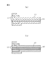
【0054】
図8に、ノイズレベルの変化率に応じて、線間隔を変更してノイズ可視化表示する例を示した。同図の(a)では、線間隔が標準の場合を、(b)では、線間隔が狭められた場合を示している。そして、図9に、ノイズレベルの変化率に応じてノイズ可視化の表示形態を変更する処理動作のフローチャートを示した。
先ず、ノイズデータ用パーソナルコンピュータ41は、アンテナ43からスペクトラム・アナライザ42を介して送られてくる微小アンテナで測定されたノイズ電圧を監視している(ステップS11)。この監視は、アンテナ43のスキャンエリアSの全域について行われ、隣り合う微小アンテナからのノイズ電圧に基づいてその変化率を演算する。
【0055】
このノイズ電圧の変化率について、予め設定した所定の閾値と比較し、この閾値に対する大小で、線間隔を変更するかどうかを判定し、変更の必要がある領域を決める(ステップS12)。
このとき、ノイズ電圧の変化率が所定値より小さい場合(変化率小)、ハッチングの線間隔を標準とし(ステップS13)、CAD用パーソナルコンピュータ51のモニタ画面に反映させる(ステップS15)。
【0056】
一方、ステップS12において、ノイズ電圧の変化率が所定値より大きい場合(変化率大)、ハッチングの線間隔を縮小して狭くし(ステップS14)、CAD用パーソナルコンピュータ51のモニタ画面に反映させる(ステップS15)。
この様子を、図8に、図7に表示された例を用いて示した。ノイズ電圧の変化率が所定値より小さい場合(変化率小)、同図の(a)に示されるように、ハッチングの線間隔は標準で表示される。図7の表示例によるノイズ発生経路を示している領域である縦16−21について見ると、図示のような赤色領域R1、橙色領域O1及び黄色領域Y1となっている。
【0057】
ところが、縦18−20の領域において、ノイズ電圧の変化率は所定閾値より大となっている場合には、同図の(b)に示されるように、(a)の標準の線間隔より狭いハッチングとする。そのハンチングされる領域は、赤色領域R2、橙色領域O2,及び黄色領域Y2のようになる。
ここで、ハッチング領域における線間隔の変更は、ノイズ電圧の変化率が所定値を超える連続した同色の領域について行われ、例えば、図7の縦2−10の領域に対してはその間隔は変更されない。これによって、急激に変化しているノイズ発生経路だけを強調することができる。勿論、図7の縦2−10の領域でも、ノイズ電圧変化率が所定閾値を超える領域を含んでいれば、線間隔が変更される。
【0058】
これまで、ノイズ発生経路の視認性を優先する場合の例を説明したが、次に、プリント基板に係る電子部品や配線パターンのレイアウトの視認性を優先する場合について、図10及び図11を参照して説明する。
上述したのと同様に、図7のノイズ発生経路の表示例を用いて、縦3−6、横G−Kにおいて、電子部品が混み合っているとする。この領域については、他の領域と比較して特にそのレイアウトの視認性が求められることになる。そこで、CADによる当該プリント基板の設計データ中に、この領域に対しては、電子部品が混み合っている、或いは、配線パターンが複雑又は高密度である等の集中度を示す属性情報を入力しておく。
【0059】
CAD用パーソナルコンピュータ51のモニタ画面に、図7に示されるようなノイズ可視化図を表示するとき、読み出された集中度に基づいて、当該領域に係るハッチングの線間隔を変更するようにする。この様にすることにより、CADレイアウトを監視しておくと、プリント基板における配線パターンが混み合っている、或いは、電子部品が集中的に実装されている等の領域について、自動的にノイズ発生経路表示のハッチング間隔を広く変更でき、配線パターンや電子部品等の視認性を向上することができる。
【0060】
図10に、配線パターンや電子部品の混み具合を示すCADレイアウトの集中度に応じて、線間隔を変更してノイズ可視化表示する例を示した。同図の(a)では、線間隔が標準の場合を、(b)では、線間隔が拡大された場合を示している。そして、図11に、CADレイアウトの集中度に応じて、ノイズ可視化の表示形態を変更する処理動作のフローチャートを示した。
【0061】
先ず、CAD用パーソナルコンピュータ51は、試験対象となっているプリント基板に係るCADデータに基づいてCADレイアウトを監視している(ステップS21)。この監視は、CADレイアウトの集中度が当該プリント基板においてどうなっているかを読み出すものである。
当該プリント基板について読み出された集中度を予め設定入力された所定値と比較し、ハッチングの線間隔を変更する必要があるかどうかについて、当該プリント基板上の表示領域毎に判定を行う(ステップS22)。
【0062】
このとき、集中度が所定値より小さい場合(集中度小)、ハッチングの線間隔を標準とし(ステップS23)、CAD用パーソナルコンピュータ51のモニタ画面に反映させる(ステップS25)。
一方、ステップS22において、集中度が所定値より大きい場合(集中度大)、ハッチングの線間隔を拡大して広くし(ステップS24)、CAD用パーソナルコンピュータ51のモニタ画面に反映させる(ステップS25)。
【0063】
この様子を、図10に、図7に表示された例を用いて示した。集中度が所定値より小さい場合(集中度小)、同図の(a)に示されるように、ハッチングの線間隔は標準で表示されることになる。図7の表示例によるノイズ発生経路の状況を示す縦2−6の領域について見ると、図示のような橙色領域O3及び黄色領域Y3となる。
【0064】
ところが、縦2−6の領域において、読み出された集中度が所定値より大となっている場合には、同図の(b)に示されるように、(a)の標準の線間隔より広いハッチングとする。そのハッチング領域は、橙色領域O4及び黄色領域Y4のようになる。
ここで、ハッチング領域における線間隔の変更は、集中度が所定値を超えているハッチング領域であって、変更対象の領域に連続した領域について行われる。例えば、図7の縦16−21のハッチング領域では、集中度が所定値を超えておらず、変更対象領域とも離れているので、その領域における線間隔は変更されない。
【0065】
これによって、配線パターン又は電子部品が混み合っている部位について、ノイズ発生経路の状況を把握しつつ、視認性を向上することができる。勿論、図7の縦16−21の領域でも、集中度が所定値を超える領域を含んでいれば、線間隔が変更される。
以上のように、図7に示されるようなノイズ可視化表示について、その表示領域をハッチングで表したとき、ノイズ電圧の変化率又はCADレイアウトの集中度のどちらかを監視し、それらの度合いに応じて、ハッチングの線間隔を変更することにより、ノイズ発生経路状況を強調し、又は基板パターン、電子部品等の混み具合を目立たせ、そのどちらかを優先的に表示画面での視認性を向上するものであった。
【0066】
しかし、種々のプリント基板の中には、例えば、ノイズ電圧の変化率が大きい領域と、CADレイアウトの集中度が高い領域とが共に重なっている場合が有り得る。このような場合に、上述したようなノイズ電圧の変化率とCADレイアウトの集中度のどちらかを優先的に監視することになると、相反する方向にハッチング線間隔を変更することになるため、ノイズ可視化表示画面での視認性向上を混乱させる。
【0067】
そこで、これらの表示状態条件の両方を共に必要とする場合であっても、ノイズ可視化表示において、中間的なハッチング線間隔を用意し、監視条件に応じて自動的に線間隔を変更制御できるようにした。
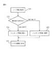
図12に、ノイズ電圧の変化率とCADレイアウトパターンの集中度とを同時に監視し、その表示状態条件に応じてノイズ可視化の表示形態を変更する処理動作を説明するフローチャートを示した。
【0068】
先ず、ステップS31において、ノイズ電圧の変化率とCADレイアウトの集中度の両方を監視する。ノイズ電圧の変化率及びCADレイアウトの集中度の監視は、図9及び図11の各監視と同様の手順で行われるが、これらは、ノイズ可視化表示の際に同時に考慮される。
次に、ステップS32において、検出されたノイズ電圧の変化率と読み出されたCADレイアウトの集中度の判定を、それぞれの所定値に対する大小比較で行う。これらの大小の組み合わせにより、監視条件に応じた表示状態の場合分けがされる。
【0069】
電圧変化率が小で、レイアウト集中度が大である場合には(変化率小、集中度大)、表示領域のハッチング線間隔を拡大して広くする(ステップS33)。そして、当該領域の表示状態について、この線間隔によるハッチングがCAD画面に反映される(ステップS36)。この場合は、図7に示された例によれば、縦2−10に適用される。
【0070】
ステップS32において、電圧変化率が大で、レイアウト集中度が小である場合には(変化率大、集中度小)、表示領域のハッチング線間隔を縮小して狭くする(ステップS34)。そして、当該領域の表示状態について、この線間隔によるハッチングがCAD画面に反映される(ステップS36)。この場合は、図7に示された例によれば、縦16−21に適用される。
【0071】
次に、ステップS32において、電圧変化率が大で、レイアウト集中度も大である場合には(変化率大、集中度大)、当該表示領域のハッチングの線間隔を標準のままとする(ステップS35)。この場合は、視認性を向上するとすれば、ノイズ発生経路状況の観点では、線間隔を狭く、そして、レイアウトの混み具合の観点からは、線間隔を広くする必要があるが、双方の条件に従って同時には表示することができないので、表示画面上では、双方の条件を取り入れて中間的なものとして、当該領域のハッチングの線間隔を標準とする。
【0072】
また、電圧変化率が小で、レイアウト集中度も小である場合には(変化率小、集中度小)、特に、視認性向上を要しないとして、当該領域のハッチングの線間隔を標準とする(ステップS35)。そして、これらの表示状態について、標準の線間隔によるハッチングがCAD画面に反映される(ステップS36)。
このように、プリント基板から検出されたノイズ電圧の変化率から、ノイズ発生経路状況を判定し、当該プリント基板のCAD設計データに基づいて配線パターンや電子部品に係るレイアウトの混み具合を判定するようにしたので、この判定に応じて様々なノイズ発生経路の表示形態を選択することができる。
【0073】
なお、これまで、ノイズ可視化表示に関して、そのノイズレベルをランク分けした色でノイズ表示領域を表し、その領域を所定間隔の線によるハッチングで示した。そして、その線自体の幅については、一定のものとした。
しかし、表示状態の視認性を向上できるものであれば、一定幅による線の密度を変更することに限られず、例えば、線密度は一定とし、線幅を変更するものであってもよい。また、線密度と線幅の両方の変更を採用することもできる。
【0074】
さらに、ハッチングではなく、丸形、四角形等によるドットによってノイズの可視化をすることができ、このドットにノイズレベルのランクに対応した色を割り当て、ノイズ発生経路状況をそのドットで表示し、ドットの密度又はドットの大小を変更するようにしてもよい。
以上のとおり、本発明の実施形態によるノイズ可視化システムによれば、検出されたノイズデータとCADによる設計データとが合成され、ノイズ可視化表示による画像によってノイズ発生経路を検証することができ、試験対象物であるプリント基板等が予想される電磁環境下において誤動作しないかどうかを、表示画面上でその状況を視認することができる。そして、誤動作する可能性を見出した場合には、対象となる高周波ノイズに対して誤動作が発生しないように、表示画像から明確に位置が特定される箇所を中心に、回路パターンの変更や電子部品自体の変更等の対策を講じることができる。
【0075】
さらに、CADデータを用いているので、試験対象物の表面のみではなく、電子部品の配置図またはプリント配線パターンとノイズデータとを合成すること等が可能となり、効率的に誤動作が発生する箇所の特定が図られることとなった。特に、重層基板の場合には、表面からでは見ることができない中間層におけるプリント配線基板等とノイズデータを合成することができるので、より効率的に誤動作が発生する箇所の特定が図られる。
【0076】
また、プリント基板上に配置されたマイコン等のクロックを原因とする通常動作時における試験対象物自らの放射(又は伝導)ノイズ(エミッション)においても、同システムにより、画像から明確に位置が特定された箇所を中心に回路パターンの変更や電子部品自体の変更等を行える。このような通常動作時における試験対象物自らの放射(又は伝導)ノイズを検出するには、試験対象物の通常動作が行われるような信号(例えば電源電庄)を、ワイヤ・ハーネスを介してプリント基板に対して注入し、試験対象物を通常動作させ、このときにおいて試験対象物自らの放射(又は伝導)ノイズをアンテナにて検出させるようにすればよい。
【0077】
さらに、ノイズ可視化表示した画像によって、プリント基板の配線パターンや電子部品等の装着位置に対応させてノイズ発生経路を簡単に検証することができ、その検証時において、ノイズ発生経路の状況を、ノイズ電圧の変化率又はレイアウトの集中度に応じて、ノイズ発生経路の領域の表示形態を変更するようにしたので、ノイズ発生経路状況又はプリント基板自体のレイアウトに関する表示画面の視認性を向上することができた。
【0079】
更に、ノイズ試験として、ノイズ注入又は電子部品からのノイズ測定を前提としているが、これに限らず、シミュレーションにより電子部品から発生するノイズを予測するノイズシミュレータを前提としても良い。
【0080】
【発明の効果】
このように、試験対象物から放射される高周波ノイズのノイズデータと試験対象物のCAD設計データを合成し、試験対象物上で高周波ノイズが注入される経路や、誤動作が発生する可能性の高い領域、配線パターン、電子部品等の位置を明確に特定することができる。
【0081】
したがって、イミュニティ試験やエミッション試験の前に(場合によっては後に)、そのような誤動作が発生しない回路に設計変更する場合に、従来のトライ・アンド・エラー方式を採用する必要が無くなり、設計の効率化及び試験工数の削減が図られることとなった。
本発明のノイズ可視化システム及びその表示方法によれば、得られたノイズデータと試験対象物の設計データとを合成することができ、ノイズ発生経路状況を試験対象物の画像中に表示するようにして、ノイズ可視化画像の視認性を向上させることができる。
【0082】
さらに、得られたノイズデータの変化率又は試験対象物の設計データであるCADデータの集中度に応じてノイズ画像の表示形態を変更することにより、ノイズ可視化画像の視認性を向上させることができる。
【図面の簡単な説明】
【図1】従来技術における試験方法の概略を示す図である。
【図2】別の従来技術における試験方法の概略を示す図である。
【図3】本発明に係わるノイズ可視化システムの概略構成を示す図である。
【図4】本発明に係わるノイズ可視化システムの具体的構成の一部を拡大して示した図である。
【図5】本発明に係るノイズ可視化システムにおいて測定されたノイズデータの画像の一例を示す図である。
【図6】設計されたプリント基板に係るCADデータの画像の一例を示す図である。
【図7】本発明に係わるノイズ可視化システムにおいてノイズデータとCADデータを合成した画像の一例を示す図である。
【図8】図7に示された画像中でノイズ電圧の変化率が大きい部位に関するノイズ可視化表示の変更例を示す図である。
【図9】ノイズ電圧の変化率に応じてノイズ可視化の表示形態を変更する処理動作を説明するフローチャートを示す図である。
【図10】図7に示された画像中でCADレイアウトパターンの集中度が大きい部位に関するノイズ可視化表示の変更例を示す図である。
【図11】CADレイアウトパターンの集中度に応じてノイズ可視化の表示形態を変更する処理動作を説明するフローチャートを示す図である。
【図12】ノイズ電圧の変化率とCADレイアウトパターンの集中度を考慮してノイズ可視化の表示形態を変更する処理動作を説明するフローチャートを示す図である。
【符号の説明】
10…TEMセル法における試験装置
20…アンテナ照射法における電波暗室
30…ノイズ可視化システム
31…制御用パーソナルコンピュータ
32…信号発生器
34、42…スペクトラム・アナライザ
36…モニタ・プローブ
37…インジェクション・プローブ
38…プリント基板
39…インタフェース
40…ワイヤ・ハーネス
41…ノイズデータ用パーソナルコンピュータ
43…アンテナ
51…CAD用パーソナルコンピュータ[0001]
BACKGROUND OF THE INVENTION
The present invention relates to a noise visualization system that visualizes noise information and a display method thereof.
[0002]
[Prior art]
Usually, printed circuit boards to which electronic parts such as ICs are mounted are arranged inside the electronic device, but the circuit formed on the printed circuit board is capacitively coupled to the main body of the electronic device and other substrates in the electronic device. May malfunction due to external interference such as electromagnetic coupling or external electromagnetic waves.
[0003]
The occurrence of such a malfunction in a printed circuit board or the like used in an automobile engine control unit is a fatal problem.
Therefore, in the case of printed circuit boards that have important functions, check in advance that malfunctions will not occur due to external interference, and if there is a possibility of malfunctions, malfunctions will not occur. It is necessary to make design changes. The ability of a printed circuit board or the like to withstand these without being degraded by external interference is called immunity or electromagnetic field susceptibility (EMS), and recently, to measure such resistance. The immunity test has been started.
[0004]
One method of immunity testing is the TEM cell method. The TEM cell method will be described with reference to FIG.
FIG. 1 shows a
[0005]
In the TEM cell method, various electric fields are generated in the
[0006]
However, in the TEM cell method, when the
[0007]
There is an antenna irradiation method as another method of the immunity test. The antenna irradiation method will be described with reference to FIG.
FIG. 2 shows an
[0008]
In the antenna irradiation method, various electromagnetic radiations are emitted from the
In the antenna irradiation method, since measurement is performed using a general-purpose
[0009]
In the antenna irradiation method, it is also important to suppress the radiation (or conduction) noise of the test object during normal operation due to the clock of a microcomputer or the like placed on the printed circuit board below a specified value. For this reason, it is more difficult to specify from which part of the test object the noise is radiated (or conducted).
[0010]
[Problems to be solved by the invention]
Therefore, according to the present invention, the noise test result is displayed as an image so that it is possible to easily identify which part of the test object is vulnerable to interference from the outside by overcoming the above-described problems in the prior art. It aims to provide a noise visualization system.
[0011]
Furthermore, it is possible to easily identify from which part of the test object the noise is radiated (or conducted), and to support the suppression of the radiation (or conduction) noise of the test object during normal operation. It is intended to provide a noise visualization system that can be used.
Also, the object of the present invention is to synthesize the obtained noise data and the design data of the test object, and display the noise generation path status in the image of the test object, thereby improving the visibility of the noise visualization image. An object of the present invention is to provide an improved noise visualization system and a display method thereof.
[0012]
Furthermore, a noise visualization system that improves the visibility of the noise visualization image by changing the display form of the noise image according to the level of the obtained noise data or the concentration of the CAD data that is the design data of the test object, and The display method is intended to be provided.
[0013]
[Means for Solving the Problems]
In order to solve the above problem, in the noise visualization system according to the present invention, Generated by injecting a high-frequency signal that simulates noise into the test object Noise information acquisition means for acquiring noise information, design information acquisition means for acquiring design information related to the test object stored in advance, and noise generation according to the noise information on a design image based on the design information Image display means for displaying an image, and the image display means changes a display form of the noise occurrence image according to an image display condition.
[0014]
The design information is CAD data related to the test object, and the noise information is generated by injecting a high-frequency signal that simulates noise into the test object or the test object is in operation. The noise generation image is represented by a display area divided according to a noise level included in the noise information.
[0015]
Further, when the image display condition is a change rate or absolute value of the noise level, and the image display means changes a display form of the noise occurrence image when the change rate related to the display area is larger than a predetermined value. And the image display condition is a layout concentration degree included in the design information, and the image display means displays a display form of the noise generation image corresponding to a part where the layout concentration degree is larger than a predetermined value. Change and display. Alternatively, the image display condition is a change rate or absolute value of the noise level and a layout concentration included in the design information, and the image display means is a display form set corresponding to a combination of the two conditions. And the noise generation image is displayed. The display mode is changed by changing the hatching line interval or line width.
[0016]
In the noise visualization display method according to the present invention, Generated by injecting a high-frequency signal that simulates noise into the test object Noise information and design information related to the test object stored in advance are acquired, a noise generation image based on the noise information is displayed on a design image based on the design information, and the noise generation image The display area is divided according to the information, and the display form is changed according to the image display condition.
[0017]
The design information is CAD data related to the test object, and the noise information is generated when a high-frequency signal simulating noise is injected into the test object or the test object is in operation. It was assumed that it occurred.
Further, when the image display condition is a change rate or an absolute value of the noise level, and the change rate related to the display area is larger than a predetermined value, the display form of the noise occurrence image is changed, and the image display condition Is the layout concentration level included in the design information, and the display form of the noise generation image corresponding to the part where the layout concentration level is larger than a predetermined value is changed. Alternatively, the image display condition is a change rate or absolute value of the noise level and a layout concentration included in the design information, and the noise generation image is set in a display form set corresponding to the combination of both conditions. Changed to display. The display form is changed by changing the hatching line interval or line width.
Further, as a noise visualization device according to the noise visualization display method of the present invention, for a design image based on design information relating to a test object stored in advance, Generated by injecting a high-frequency signal that simulates noise into the test object An image display means is provided for displaying a noise generation image corresponding to the noise information in an overlapping manner and changing a display form of the noise generation image according to an image display condition.
[0018]
DETAILED DESCRIPTION OF THE INVENTION
Next, an embodiment of a noise visualization system according to the present invention will be described with reference to the drawings.
In FIG. 3,
[0019]
Reference numeral 41 denotes a noise data personal computer, 42 denotes a spectrum analyzer, and 43 denotes an antenna. The
[0020]
A CAD
[0021]
In the present embodiment shown in FIG. 3, the control
In FIG. 3, a printed
[0022]
A
[0023]
The control
[0024]
FIG. 4 is a view of the printed
[0025]
Next, detection of noise data by noise visualization measurement will be described.
First, a predetermined high frequency signal is generated by the
[0026]
In this embodiment, the high frequency noise superimposed on the
[0027]
When high-frequency noise corresponding to the high-frequency signal generated by the
[0028]
The detected radiation noise is sent as detection signals to the noise data personal computer 41 via the
[0029]
The largest cause of malfunction of the printed
[0030]
The high frequency signal generated by the
[0031]
When the type and frequency of high-frequency noise that is likely to cause a malfunction are not known from the beginning with respect to the printed
[0032]
FIG. 5 shows noise data obtained by processing the detection signal from the
[0033]
The method for visualizing the detected high-frequency noise is not limited to that shown in FIG. 5, and various known methods can be employed. For example, a smoothing process is performed on the contour representing the intensity level.
Referring to FIG. 5, it can be seen that there is a region that generates particularly high-intensity high-frequency noise. That is, a large amount of injected high-frequency noise is radiated from a position corresponding to this region on the printed
[0034]
In other words, when this printed
[0035]
However, it may be difficult to specify from which part of the actual printed circuit board the high frequency noise is generated only by the noise data as shown in FIG. In particular, it is difficult to distinguish when the printed wiring pattern of the printed board is fine or when the printed board is formed in multiple layers.
Therefore, in the
[0036]
FIG. 6 shows an example of CAD data which is design data.
FIG. 6 shows a printed
[0037]
In the printed circuit board shown in FIG. 6, CAD data is drawn based on the position of the symbol “+” in the lower left. The CAD data stores design data related to the printed circuit board for one side or both sides of the printed circuit board, or for each layer when it is formed in multiple layers so that it can be read out as necessary. .
[0038]
7, the noise data shown in FIG. 5 processed by the noise data personal computer 41 is synthesized with the CAD data shown in FIG. 6, and the CAD
[0039]
FIG. 7 is a combination of electronic component arrangement data and noise data on the printed
[0040]
Next, a procedure for synthesizing detected noise data and design data in the CAD
First, the noise data personal computer 41 transmits intensity data for each minute antenna element of the
[0041]
Next, the position data of the printed
[0042]
Next, the noise data transmitted from the noise data personal computer 41 to the CAD
Next, CAD data which is design data of the printed
[0043]
Next, the origin alignment is performed so that the design reference data (B 1-24 in FIG. 6) in the CAD data of the printed
Finally, the synthesized image data is displayed on the monitor of the CAD
[0044]
In the above-described procedure, noise data having coordinate data corresponding to the position of the minute antenna element in the
In the above-described procedure, the measurer inputs the position data of the printed
[0045]
Also, the orientation of the printed circuit board in the CAD data is not always constant. For example, in the example of FIG. 6, the longitudinal direction of the board is aligned with the vertical axis in the figure, but the designer of CAD data does not always draw in this way. For example, the longitudinal direction of the printed board is shown in FIG. In some cases, the plot is made to match the horizontal axis. Therefore, it is conceivable that the direction of the noise data and the CAD data do not match only by simply performing the origin position alignment. Therefore, it is preferable that the noise data can be rotated while the origin is aligned and synthesized with the CAD data.
[0046]
Preferably, the noise data can be rotated at least 90, 180 and 270 degrees. The rotation is performed in accordance with a known image processing method. However, it may be performed by an instruction from the operator's keyboard, or the computer automatically determines the direction of noise data and CAD data. The noise data may be automatically rotated. Further, CAD data may be rotated instead of noise data.
[0047]
In addition to CAD data, other data can be used as design data. However, at least design reference data is necessary to perform origin position alignment with noise data.
As described above, in the noise visualization system according to the present embodiment shown in FIGS. 3 and 4, as shown in FIG. 7, the noise data detected by the
[0048]
However, on the printed
For the printed circuit board in such a situation, in FIG. 7, the distribution of detected noise data intensity is indicated by white, gray, and black shadows according to the four levels of density shown in FIG. . However, in FIG. 7, images of variously arranged electronic components or wiring patterns overlap with images of the noise generation path status, and visibility is deteriorated.
[0049]
Further, the noise generation distribution may be displayed with a plurality of colors corresponding to the intensity level, for example, as the intensity level of the noise data instead of the monochrome density level. Taking FIG. 7 as an example, instead of black and white shadows, for example, the strongest level may be displayed in red, then orange, yellow, and the weakest level in colorless.
[0050]
At this time, if the images of variously arranged electronic components or wiring patterns and the image of the noise generation path status are superimposed, the arrangement of the electronic components etc. can be seen directly in the colorless area, but noise is generated. An electronic component or the like located in the area that is covered is hidden by the color for displaying the noise intensity level. When noise is generated over a wide range, the visibility is deteriorated particularly when trying to grasp the relationship between the state of occurrence and electronic components.
[0051]
Therefore, in the noise visualization system according to the present embodiment, the display method of the noise intensity level in the visualization is further improved to improve the visibility of the image. This display method will be described with reference to FIGS.
Here, a case where a noise generation distribution is displayed using a plurality of colors corresponding to the detected noise intensity level will be described with reference to FIG. In the figure, the density is expressed by black and white density. For example, the strongest level is displayed as red R, then orange O, yellow Y, and the weakest level is colorless.
[0052]
In the visualization display method adopted here, the hatching line interval by the color line of the noise visualization diagram displayed for the noise generation path status can be arbitrarily changed according to the display state condition. For example, in order to place importance on the visibility of electronic components placed on a printed circuit board, the noise detection area is displayed with line information by hatching that is distinguished by color. However, the electronic components on the printed circuit board are displayed between the lines, and the visibility is improved. Since there are a plurality of lines distinguished by colors in the area, the state of the noise generation path can be grasped.
[0053]
Furthermore, in a region where the change in the noise level is large, it indicates that the noise is concentrated. In this case, the line interval is narrowed and the noise generation path is emphasized. In addition, a region where the electronic parts and wiring patterns on the printed circuit board are crowded is displayed with a wide line interval to make it easy to see the state of the substrate surface.
As described above, the visibility is improved by changing the line interval by hatching according to the display state condition in consideration of the noise level change rate and the substrate surface state.
[0054]
FIG. 8 shows an example in which noise is visualized by changing the line interval according to the change rate of the noise level. (A) of the figure shows the case where the line spacing is standard, and (b) shows the case where the line spacing is narrowed. FIG. 9 shows a flowchart of the processing operation for changing the display form of the noise visualization according to the change rate of the noise level.
First, the noise data personal computer 41 monitors the noise voltage measured by the minute antenna sent from the
[0055]
The change rate of the noise voltage is compared with a predetermined threshold value that is set in advance, and it is determined whether or not the line interval is to be changed depending on the magnitude of the threshold value, and an area that needs to be changed is determined (step S12).
At this time, when the change rate of the noise voltage is smaller than a predetermined value (change rate is small), the hatched line interval is set as a standard (step S13) and reflected on the monitor screen of the CAD personal computer 51 (step S15).
[0056]
On the other hand, if the change rate of the noise voltage is larger than the predetermined value in step S12 (large change rate), the hatching line interval is reduced and narrowed (step S14) and reflected on the monitor screen of the CAD personal computer 51 ( Step S15).
This is shown in FIG. 8 using the example shown in FIG. When the change rate of the noise voltage is smaller than a predetermined value (change rate is small), the hatched line interval is displayed as a standard as shown in FIG. Looking at the vertical 16-21, which is a region showing the noise generation path according to the display example of FIG. 7, a red region R1, an orange region O1, and a yellow region Y1 as shown in the figure are obtained.
[0057]
However, when the change rate of the noise voltage is larger than the predetermined threshold in the vertical 18-20 region, as shown in FIG. 5B, it is narrower than the standard line spacing of FIG. It shall be hatched. The hunted areas are red area R2, orange area O2, and yellow area Y2.
Here, the change of the line interval in the hatching region is performed for the same color region where the change rate of the noise voltage exceeds a predetermined value. For example, the interval is changed for the vertical 2-10 region in FIG. Not. As a result, it is possible to emphasize only the noise generation path that is changing rapidly. Of course, even in the region of length 2-10 in FIG. 7, the line spacing is changed if the noise voltage change rate includes a region exceeding a predetermined threshold.
[0058]
The example in the case where priority is given to the visibility of the noise generation path has been described so far. Next, in the case of giving priority to the visibility of the layout of the electronic component and the wiring pattern related to the printed circuit board, refer to FIGS. To explain.
In the same manner as described above, it is assumed that electronic components are crowded in the vertical 3-6 and the horizontal GK using the display example of the noise generation path in FIG. For this region, the visibility of the layout is particularly required as compared with other regions. Therefore, in the design data of the printed circuit board by CAD, attribute information indicating the degree of concentration, such as electronic parts being crowded or wiring patterns being complex or high density, is input to this area. Keep it.
[0059]
When the noise visualization diagram as shown in FIG. 7 is displayed on the monitor screen of the CAD
[0060]
FIG. 10 shows an example in which noise is visualized by changing the line spacing in accordance with the concentration degree of the CAD layout indicating the degree of congestion of wiring patterns and electronic components. (A) of the figure shows a case where the line spacing is standard, and (b) shows a case where the line spacing is enlarged. FIG. 11 shows a flowchart of the processing operation for changing the display form of the noise visualization according to the concentration degree of the CAD layout.
[0061]
First, the CAD
The degree of concentration read for the printed circuit board is compared with a predetermined value input in advance, and it is determined for each display area on the printed circuit board whether or not the hatching line interval needs to be changed (step) S22).
[0062]
At this time, if the degree of concentration is smaller than a predetermined value (concentration level is low), the hatched line interval is set as a standard (step S23) and reflected on the monitor screen of the CAD personal computer 51 (step S25).
On the other hand, if the concentration is greater than the predetermined value (high concentration) in step S22, the hatching line interval is enlarged and widened (step S24) and reflected on the monitor screen of the CAD personal computer 51 (step S25). .
[0063]
This is shown in FIG. 10 using the example shown in FIG. When the concentration level is smaller than a predetermined value (low concentration level), the hatched line spacing is displayed as a standard as shown in FIG. When viewing the vertical 2-6 region indicating the state of the noise generation path according to the display example of FIG. 7, an orange region O3 and a yellow region Y3 as illustrated are obtained.
[0064]
However, when the read concentration is larger than a predetermined value in the vertical 2-6 region, as shown in FIG. Wide hatching. The hatched areas are an orange area O4 and a yellow area Y4.
Here, the change of the line interval in the hatching area is performed in the hatching area where the degree of concentration exceeds a predetermined value and the area continuous with the area to be changed. For example, in the vertical 16-21 hatched area in FIG. 7, the concentration does not exceed a predetermined value and is away from the area to be changed, so the line spacing in that area is not changed.
[0065]
As a result, it is possible to improve the visibility while grasping the state of the noise generation path for the part where the wiring pattern or the electronic component is crowded. Of course, even in the vertical 16-21 region of FIG. 7, the line spacing is changed if the concentration level includes a region exceeding the predetermined value.
As described above, when the display area of the noise visualization display as shown in FIG. 7 is represented by hatching, either the change rate of the noise voltage or the concentration of the CAD layout is monitored, and according to the degree. By changing the hatching line spacing, the noise generation path situation is emphasized, or the congestion of the substrate pattern, electronic parts, etc. is made conspicuous, and either of them is preferentially improved on the display screen. It was a thing.
[0066]
However, in various printed boards, for example, there may be a case where an area where the change rate of the noise voltage is large overlaps an area where the CAD layout is highly concentrated. In such a case, if one of the above-described noise voltage change rate and CAD layout concentration level is preferentially monitored, the hatching line interval is changed in the opposite direction. It disrupts the visibility improvement on the visualization display screen.
[0067]
Therefore, even when both of these display state conditions are required, an intermediate hatching line interval is prepared in the noise visualization display, and the line interval can be automatically changed and controlled according to the monitoring condition. I made it.
FIG. 12 shows a flowchart for explaining the processing operation for simultaneously monitoring the change rate of the noise voltage and the concentration degree of the CAD layout pattern and changing the display form of the noise visualization according to the display state condition.
[0068]
First, in step S31, both the noise voltage change rate and the CAD layout concentration are monitored. Monitoring of the change rate of the noise voltage and the degree of concentration of the CAD layout is performed in the same procedure as each of the monitoring in FIGS. 9 and 11, but these are considered simultaneously in the noise visualization display.
Next, in step S32, the change rate of the detected noise voltage and the degree of concentration of the read CAD layout are determined by comparing the magnitudes of the respective predetermined values. Depending on the combination of these sizes, the display states according to the monitoring conditions are divided.
[0069]
If the voltage change rate is small and the layout concentration is large (low change rate, high concentration), the hatching line interval in the display area is enlarged and widened (step S33). And about the display state of the said area | region, the hatching by this line interval is reflected on a CAD screen (step S36). In this case, according to the example shown in FIG.
[0070]
In step S32, when the voltage change rate is large and the layout concentration is low (high change rate, low concentration), the hatching line interval of the display area is reduced and narrowed (step S34). And about the display state of the said area | region, the hatching by this line interval is reflected on a CAD screen (step S36). In this case, according to the example shown in FIG.
[0071]
Next, in step S32, when the voltage change rate is large and the layout concentration is also large (large change rate, high concentration), the hatching line interval of the display area remains the standard (step S35). In this case, if the visibility is improved, it is necessary to reduce the line interval from the viewpoint of the noise generation path situation, and it is necessary to increase the line interval from the viewpoint of the congestion of the layout. Since they cannot be displayed at the same time, on the display screen, both conditions are taken in as an intermediate, and the hatching line interval of the area is set as a standard.
[0072]
In addition, when the voltage change rate is small and the layout concentration level is also low (change rate is low, concentration level is low), the line spacing of the hatching in the area is set as a standard, especially when no improvement in visibility is required. (Step S35). And about these display states, the hatching by a standard line interval is reflected on a CAD screen (step S36).
In this way, the noise generation path status is determined from the rate of change of the noise voltage detected from the printed circuit board, and the degree of congestion of the layout related to the wiring pattern or electronic component is determined based on the CAD design data of the printed circuit board. Therefore, various display forms of noise generation paths can be selected according to this determination.
[0073]
Heretofore, regarding the noise visualization display, the noise display area is represented by a color obtained by ranking the noise level, and the area is indicated by hatching with a line of a predetermined interval. The width of the line itself is fixed.
However, as long as the visibility of the display state can be improved, the line density is not limited to a constant width. For example, the line density may be constant and the line width may be changed. It is also possible to adopt changes in both line density and line width.
[0074]
In addition, noise can be visualized by dots such as circles and squares instead of hatching, and a color corresponding to the rank of the noise level is assigned to this dot, and the noise generation path status is displayed with that dot, and the dot The density or the size of the dots may be changed.
As described above, according to the noise visualization system according to the embodiment of the present invention, the detected noise data and the design data by CAD are synthesized, and the noise generation path can be verified by the image by the noise visualization display. Whether a printed circuit board or the like, which is an object, does not malfunction in an expected electromagnetic environment, can be visually confirmed on the display screen. And if there is a possibility of malfunction, circuit pattern changes and electronic components are centered around the location where the position is clearly identified from the display image so that malfunction does not occur for the target high-frequency noise. Measures such as changes of itself can be taken.
[0075]
Furthermore, since CAD data is used, it is possible to synthesize not only the surface of the test object but also the layout drawing of electronic parts or printed wiring pattern and noise data, etc. It was decided to be specific. In particular, in the case of a multi-layer board, noise data can be synthesized with a printed wiring board or the like in an intermediate layer that cannot be seen from the surface, so that a location where a malfunction occurs can be identified more efficiently.
[0076]
The system also clearly identifies the position of the test object's own radiated (or conducted) noise (emission) during normal operation caused by a clock such as a microcomputer placed on the printed circuit board from the image. It is possible to change the circuit pattern, change the electronic component itself, etc., centering on the location. In order to detect the radiation (or conduction) noise of the test object itself during such normal operation, a signal (for example, a power supply voltage) that causes the normal operation of the test object is transmitted via the wire harness. The test object is injected into the printed circuit board, and the test object is normally operated. At this time, the radiation (or conduction) noise of the test object itself may be detected by the antenna.
[0077]
Furthermore, the noise generation path can be easily verified with the noise visualized image corresponding to the wiring pattern of the printed circuit board or the mounting position of the electronic component. At the time of the verification, the state of the noise generation path is Since the display form of the noise generation path area is changed according to the voltage change rate or the layout concentration, the visibility of the display screen regarding the noise generation path status or the layout of the printed circuit board itself can be improved. did it.
[0079]
Furthermore, the noise test is premised on noise injection or noise measurement from electronic components, but is not limited to this, and may be premised on a noise simulator that predicts noise generated from electronic components by simulation.
[0080]
【The invention's effect】
As described above, the noise data of the high frequency noise radiated from the test object and the CAD design data of the test object are synthesized, and the path through which the high frequency noise is injected on the test object or malfunction is likely to occur. The positions of areas, wiring patterns, electronic components, etc. can be clearly identified.
[0081]
Therefore, it is not necessary to adopt the conventional try-and-error method when changing the design to a circuit that does not cause such malfunctions before (or in some cases) before the immunity test and emission test. And reduction of test man-hours.
According to the noise visualization system and the display method thereof of the present invention, the obtained noise data and the design data of the test object can be synthesized, and the noise generation path state is displayed in the image of the test object. Thus, the visibility of the noise visualized image can be improved.
[0082]
Furthermore, the visibility of the noise visualized image can be improved by changing the display form of the noise image in accordance with the rate of change of the obtained noise data or the concentration of CAD data that is design data of the test object. .
[Brief description of the drawings]
FIG. 1 is a diagram showing an outline of a test method in the prior art.
FIG. 2 is a diagram showing an outline of a test method in another conventional technique.
FIG. 3 is a diagram showing a schematic configuration of a noise visualization system according to the present invention.
FIG. 4 is an enlarged view showing a part of a specific configuration of a noise visualization system according to the present invention.
FIG. 5 is a diagram showing an example of an image of noise data measured in the noise visualization system according to the present invention.
FIG. 6 is a diagram illustrating an example of an image of CAD data relating to a designed printed circuit board.
FIG. 7 is a diagram showing an example of an image obtained by combining noise data and CAD data in the noise visualization system according to the present invention.
FIG. 8 is a diagram illustrating a change example of the noise visualization display regarding a portion where the change rate of the noise voltage is large in the image shown in FIG. 7;
FIG. 9 is a flowchart illustrating a processing operation for changing a display form of noise visualization according to a change rate of a noise voltage.
10 is a diagram showing an example of a change in noise visualization display related to a portion where the CAD layout pattern is highly concentrated in the image shown in FIG. 7;
FIG. 11 is a flowchart illustrating a processing operation for changing a noise visualization display form in accordance with the concentration level of a CAD layout pattern.
FIG. 12 is a flowchart illustrating a processing operation for changing a display form of noise visualization in consideration of a change rate of a noise voltage and a concentration degree of a CAD layout pattern.
[Explanation of symbols]
10 ... Test equipment in TEM cell method
20 ... Anechoic chamber in antenna irradiation method
30 ... Noise visualization system
31 ... Control personal computer
32 ... Signal generator
34, 42 ... Spectrum analyzer
36 ... Monitor probe
37 ... Injection probe
38 ... Printed circuit board
39 ... Interface
40 ... Wire harness
41 ... Personal computer for noise data
43 ... Antenna
51. Personal computer for CAD
Claims (16)
予め記憶された前記試験対象物に係る設計情報を取得する設計情報取得手段と、
前記設計情報に基づく設計画像上に、前記ノイズ情報に応じたノイズ発生画像を表示する画像表示手段とを有し、
前記画像表示手段は、前記ノイズ発生画像の表示形態を画像表示条件に応じて変更するノイズ可視化システム。Noise information acquisition means for acquiring noise information generated by injecting a high-frequency signal that simulates noise into the test object ;
Design information acquisition means for acquiring design information related to the test object stored in advance;
On the design image based on the design information, having an image display means for displaying a noise generation image according to the noise information,
The noise display system, wherein the image display means changes a display form of the noise occurrence image according to an image display condition.
前記表示領域に係る前記変化率又は絶対値が所定値より大きいとき、当該ノイズ発生画像の表示形態を変更する請求項10又は11に記載のノイズ可視化表示方法。The image display condition is a change rate or absolute value of the noise level,
The noise visualization display method according to claim 10 or 11 , wherein when the rate of change or the absolute value of the display area is larger than a predetermined value, the display form of the noise occurrence image is changed.
前記レイアウト集中度が所定値より大きい部位に対応する当該ノイズ発生画像の表示形態を変更する請求項10乃至12のいずれか一項に記載のノイズ可視化表示方法。The image display condition is a layout concentration degree included in the design information,
The noise visualization display method according to any one of claims 10 to 12 , wherein a display form of the noise occurrence image corresponding to a portion where the layout concentration degree is larger than a predetermined value is changed.
Priority Applications (1)
| Application Number | Priority Date | Filing Date | Title |
|---|---|---|---|
| JP2001124822A JP3775999B2 (en) | 2001-04-23 | 2001-04-23 | Noise visualization system and display method thereof |
Applications Claiming Priority (1)
| Application Number | Priority Date | Filing Date | Title |
|---|---|---|---|
| JP2001124822A JP3775999B2 (en) | 2001-04-23 | 2001-04-23 | Noise visualization system and display method thereof |
Publications (3)
| Publication Number | Publication Date |
|---|---|
| JP2002318253A JP2002318253A (en) | 2002-10-31 |
| JP2002318253A5 JP2002318253A5 (en) | 2005-04-07 |
| JP3775999B2 true JP3775999B2 (en) | 2006-05-17 |
Family
ID=18974144
Family Applications (1)
| Application Number | Title | Priority Date | Filing Date |
|---|---|---|---|
| JP2001124822A Expired - Fee Related JP3775999B2 (en) | 2001-04-23 | 2001-04-23 | Noise visualization system and display method thereof |
Country Status (1)
| Country | Link |
|---|---|
| JP (1) | JP3775999B2 (en) |
Cited By (1)
| Publication number | Priority date | Publication date | Assignee | Title |
|---|---|---|---|---|
| CN107966643A (en) * | 2017-10-18 | 2018-04-27 | 中山大学 | The Interactive Visualization device and its implementation of a kind of real-time testing data |
Families Citing this family (8)
| Publication number | Priority date | Publication date | Assignee | Title |
|---|---|---|---|---|
| US7355413B2 (en) | 2005-01-31 | 2008-04-08 | Ricoh Company, Ltd. | Testing method/arrangement measuring electromagnetic interference of noise in a to-be-tested printed circuit board |
| US7598747B2 (en) | 2006-01-27 | 2009-10-06 | Ricoh Company, Ltd. | Noise injection apparatus for printed circuit board |
| JP5428469B2 (en) * | 2009-03-31 | 2014-02-26 | 富士通株式会社 | Shielding inspection method, shielding inspection apparatus, and shielding inspection program |
| JP5921169B2 (en) * | 2010-12-13 | 2016-05-24 | 三菱電機株式会社 | Electromagnetic noise distribution detector |
| JP5611875B2 (en) * | 2011-03-18 | 2014-10-22 | 株式会社Pfu | Information display device, information display method, and program |
| JP5565493B2 (en) * | 2013-04-03 | 2014-08-06 | 富士通株式会社 | Circuit design apparatus and circuit design program |
| JP6915780B2 (en) * | 2017-08-09 | 2021-08-04 | 日本電信電話株式会社 | Conduction noise visualization device and conduction noise visualization method |
| CN113870256B (en) * | 2021-12-01 | 2022-02-11 | 成都数之联科技有限公司 | PCB defect evaluation method, device, equipment and medium |
-
2001
- 2001-04-23 JP JP2001124822A patent/JP3775999B2/en not_active Expired - Fee Related
Cited By (2)
| Publication number | Priority date | Publication date | Assignee | Title |
|---|---|---|---|---|
| CN107966643A (en) * | 2017-10-18 | 2018-04-27 | 中山大学 | The Interactive Visualization device and its implementation of a kind of real-time testing data |
| CN107966643B (en) * | 2017-10-18 | 2020-09-29 | 中山大学 | Interactive visualization device for real-time test data and implementation method thereof |
Also Published As
| Publication number | Publication date |
|---|---|
| JP2002318253A (en) | 2002-10-31 |
Similar Documents
| Publication | Publication Date | Title |
|---|---|---|
| US8143903B2 (en) | Resonance scanning system and method for testing equipment for electromagnetic resonances | |
| JP3775999B2 (en) | Noise visualization system and display method thereof | |
| EP0919823A2 (en) | System for verifying signal timing accuracy on a digital testing device | |
| JP2010237099A (en) | Method and system for noise evaluation | |
| JPH0567184B2 (en) | ||
| CN110446932A (en) | The hardware testing of robot assisted | |
| CN106383273A (en) | Plane electromagnetic environment safety margin evaluation procedure method | |
| US7355417B1 (en) | Techniques for obtaining electromagnetic data from a circuit board | |
| WO1998053382A2 (en) | Testing the integrity of an electrical connection to a device using an onboard controllable signal source | |
| CN103439600A (en) | Anti-interference test monitoring system and monitoring method | |
| US20160069942A1 (en) | Internal line replaceable unit high intensity radiated field detector | |
| KR20030012746A (en) | Emi analyzer capable of analyzing and reducing each electromagnetic interference component | |
| CN108693459A (en) | Two point VI curved scannings for various circuit boards compare method for diagnosing faults | |
| JP3696008B2 (en) | Noise visualization system and method | |
| JP3696117B2 (en) | Noise visualization system and method | |
| US11609267B2 (en) | Immunity evaluation system and immunity evaluation method | |
| Silaghi et al. | Analysis of Radiated Immunity of an Automotive Display by means of Testing and Simulation | |
| US20030231145A1 (en) | Display apparatus for displaying property of electronic appliance | |
| US6100900A (en) | Displaying numerical data in various colors based upon their relative contribution to the whole | |
| US6173427B1 (en) | Immunity evaluation method and apparatus for electronic circuit device and LSI tester | |
| Rasek et al. | HIRF transfer function observations: Notes on results versus requirements and certification approach | |
| JP2001125801A (en) | Data synthesizing system for noise data and design data | |
| JPH1172523A (en) | Method and apparatus for evaluating immunity of electronic circuit element and lsi tester | |
| JP2002318254A (en) | Radiowave black box in noise visualization system | |
| Deutschmann et al. | Near field measurements to predict the electromagnetic emission of integrated circuits |
Legal Events
| Date | Code | Title | Description |
|---|---|---|---|
| A521 | Written amendment |
Free format text: JAPANESE INTERMEDIATE CODE: A523 Effective date: 20040531 |
|
| A621 | Written request for application examination |
Free format text: JAPANESE INTERMEDIATE CODE: A621 Effective date: 20040531 |
|
| A977 | Report on retrieval |
Free format text: JAPANESE INTERMEDIATE CODE: A971007 Effective date: 20050523 |
|
| A131 | Notification of reasons for refusal |
Free format text: JAPANESE INTERMEDIATE CODE: A131 Effective date: 20050531 |
|
| A521 | Written amendment |
Free format text: JAPANESE INTERMEDIATE CODE: A523 Effective date: 20050728 |
|
| A131 | Notification of reasons for refusal |
Free format text: JAPANESE INTERMEDIATE CODE: A131 Effective date: 20050920 |
|
| A521 | Written amendment |
Free format text: JAPANESE INTERMEDIATE CODE: A523 Effective date: 20051121 |
|
| TRDD | Decision of grant or rejection written | ||
| A01 | Written decision to grant a patent or to grant a registration (utility model) |
Free format text: JAPANESE INTERMEDIATE CODE: A01 Effective date: 20060124 |
|
| A61 | First payment of annual fees (during grant procedure) |
Free format text: JAPANESE INTERMEDIATE CODE: A61 Effective date: 20060221 |
|
| R150 | Certificate of patent or registration of utility model |
Ref document number: 3775999 Country of ref document: JP Free format text: JAPANESE INTERMEDIATE CODE: R150 Free format text: JAPANESE INTERMEDIATE CODE: R150 |
|
| FPAY | Renewal fee payment (event date is renewal date of database) |
Free format text: PAYMENT UNTIL: 20100303 Year of fee payment: 4 |
|
| FPAY | Renewal fee payment (event date is renewal date of database) |
Free format text: PAYMENT UNTIL: 20110303 Year of fee payment: 5 |
|
| FPAY | Renewal fee payment (event date is renewal date of database) |
Free format text: PAYMENT UNTIL: 20110303 Year of fee payment: 5 |
|
| FPAY | Renewal fee payment (event date is renewal date of database) |
Free format text: PAYMENT UNTIL: 20120303 Year of fee payment: 6 |
|
| FPAY | Renewal fee payment (event date is renewal date of database) |
Free format text: PAYMENT UNTIL: 20120303 Year of fee payment: 6 |
|
| FPAY | Renewal fee payment (event date is renewal date of database) |
Free format text: PAYMENT UNTIL: 20130303 Year of fee payment: 7 |
|
| FPAY | Renewal fee payment (event date is renewal date of database) |
Free format text: PAYMENT UNTIL: 20130303 Year of fee payment: 7 |
|
| FPAY | Renewal fee payment (event date is renewal date of database) |
Free format text: PAYMENT UNTIL: 20140303 Year of fee payment: 8 |
|
| FPAY | Renewal fee payment (event date is renewal date of database) |
Free format text: PAYMENT UNTIL: 20140303 Year of fee payment: 8 |
|
| LAPS | Cancellation because of no payment of annual fees |