JP3770542B2 - Deep ultraviolet soft X-ray projection lithography method and mask apparatus - Google Patents
Deep ultraviolet soft X-ray projection lithography method and mask apparatus Download PDFInfo
- Publication number
- JP3770542B2 JP3770542B2 JP2001512998A JP2001512998A JP3770542B2 JP 3770542 B2 JP3770542 B2 JP 3770542B2 JP 2001512998 A JP2001512998 A JP 2001512998A JP 2001512998 A JP2001512998 A JP 2001512998A JP 3770542 B2 JP3770542 B2 JP 3770542B2
- Authority
- JP
- Japan
- Prior art keywords
- glass
- mask
- wafer
- doped
- sio
- Prior art date
- Legal status (The legal status is an assumption and is not a legal conclusion. Google has not performed a legal analysis and makes no representation as to the accuracy of the status listed.)
- Expired - Lifetime
Links
- 238000000034 method Methods 0.000 title claims description 61
- 238000001459 lithography Methods 0.000 title claims description 31
- 239000011521 glass Substances 0.000 claims description 163
- VYPSYNLAJGMNEJ-UHFFFAOYSA-N Silicium dioxide Chemical compound O=[Si]=O VYPSYNLAJGMNEJ-UHFFFAOYSA-N 0.000 claims description 64
- 239000002994 raw material Substances 0.000 claims description 53
- 238000000576 coating method Methods 0.000 claims description 45
- 239000011248 coating agent Substances 0.000 claims description 44
- 238000004519 manufacturing process Methods 0.000 claims description 35
- 229910004298 SiO 2 Inorganic materials 0.000 claims description 32
- 238000005498 polishing Methods 0.000 claims description 32
- 230000005855 radiation Effects 0.000 claims description 27
- 239000000377 silicon dioxide Substances 0.000 claims description 27
- 229910052681 coesite Inorganic materials 0.000 claims description 24
- 229910052906 cristobalite Inorganic materials 0.000 claims description 24
- 229910052682 stishovite Inorganic materials 0.000 claims description 24
- 229910052905 tridymite Inorganic materials 0.000 claims description 24
- 230000007547 defect Effects 0.000 claims description 21
- ZAMOUSCENKQFHK-UHFFFAOYSA-N Chlorine atom Chemical compound [Cl] ZAMOUSCENKQFHK-UHFFFAOYSA-N 0.000 claims description 20
- 239000000460 chlorine Substances 0.000 claims description 20
- 229910052801 chlorine Inorganic materials 0.000 claims description 19
- 239000004071 soot Substances 0.000 claims description 18
- 238000010521 absorption reaction Methods 0.000 claims description 14
- 239000008119 colloidal silica Substances 0.000 claims description 14
- 238000005286 illumination Methods 0.000 claims description 14
- 238000006243 chemical reaction Methods 0.000 claims description 10
- 238000002310 reflectometry Methods 0.000 claims description 10
- 239000002019 doping agent Substances 0.000 claims description 8
- 239000000356 contaminant Substances 0.000 claims description 7
- 229910052783 alkali metal Inorganic materials 0.000 claims description 6
- 150000001340 alkali metals Chemical class 0.000 claims description 6
- 229910052784 alkaline earth metal Inorganic materials 0.000 claims description 6
- 150000001342 alkaline earth metals Chemical class 0.000 claims description 6
- 239000012535 impurity Substances 0.000 claims description 5
- 239000000463 material Substances 0.000 claims description 5
- 230000008859 change Effects 0.000 claims description 3
- 238000009826 distribution Methods 0.000 claims description 3
- 230000003746 surface roughness Effects 0.000 claims description 2
- 229910010413 TiO 2 Inorganic materials 0.000 claims 2
- 235000012239 silicon dioxide Nutrition 0.000 claims 2
- 239000000126 substance Substances 0.000 claims 2
- 238000011109 contamination Methods 0.000 claims 1
- 238000001900 extreme ultraviolet lithography Methods 0.000 claims 1
- 238000010438 heat treatment Methods 0.000 claims 1
- 230000001678 irradiating effect Effects 0.000 claims 1
- 235000012431 wafers Nutrition 0.000 description 106
- 239000010936 titanium Substances 0.000 description 61
- 229920002635 polyurethane Polymers 0.000 description 10
- 239000004814 polyurethane Substances 0.000 description 10
- GWEVSGVZZGPLCZ-UHFFFAOYSA-N Titan oxide Chemical compound O=[Ti]=O GWEVSGVZZGPLCZ-UHFFFAOYSA-N 0.000 description 8
- 229910000420 cerium oxide Inorganic materials 0.000 description 8
- BMMGVYCKOGBVEV-UHFFFAOYSA-N oxo(oxoceriooxy)cerium Chemical compound [Ce]=O.O=[Ce]=O BMMGVYCKOGBVEV-UHFFFAOYSA-N 0.000 description 8
- 230000008569 process Effects 0.000 description 8
- 239000002245 particle Substances 0.000 description 7
- 229910004356 Ti Raw Inorganic materials 0.000 description 6
- 238000002425 crystallisation Methods 0.000 description 6
- 230000008025 crystallization Effects 0.000 description 6
- 230000008021 deposition Effects 0.000 description 6
- 238000005259 measurement Methods 0.000 description 6
- 239000000758 substrate Substances 0.000 description 6
- 238000005382 thermal cycling Methods 0.000 description 6
- OGIDPMRJRNCKJF-UHFFFAOYSA-N titanium oxide Inorganic materials [Ti]=O OGIDPMRJRNCKJF-UHFFFAOYSA-N 0.000 description 6
- VXUYXOFXAQZZMF-UHFFFAOYSA-N titanium(IV) isopropoxide Chemical compound CC(C)O[Ti](OC(C)C)(OC(C)C)OC(C)C VXUYXOFXAQZZMF-UHFFFAOYSA-N 0.000 description 6
- 239000007864 aqueous solution Substances 0.000 description 5
- 239000013078 crystal Substances 0.000 description 5
- 238000001000 micrograph Methods 0.000 description 5
- IJGRMHOSHXDMSA-UHFFFAOYSA-N Atomic nitrogen Chemical compound N#N IJGRMHOSHXDMSA-UHFFFAOYSA-N 0.000 description 4
- 239000012159 carrier gas Substances 0.000 description 4
- 229910052719 titanium Inorganic materials 0.000 description 4
- 239000011449 brick Substances 0.000 description 3
- 238000001816 cooling Methods 0.000 description 3
- 238000005520 cutting process Methods 0.000 description 3
- 238000005530 etching Methods 0.000 description 3
- 239000007789 gas Substances 0.000 description 3
- 238000007689 inspection Methods 0.000 description 3
- HMMGMWAXVFQUOA-UHFFFAOYSA-N octamethylcyclotetrasiloxane Chemical compound C[Si]1(C)O[Si](C)(C)O[Si](C)(C)O[Si](C)(C)O1 HMMGMWAXVFQUOA-UHFFFAOYSA-N 0.000 description 3
- 238000012545 processing Methods 0.000 description 3
- 239000000243 solution Substances 0.000 description 3
- 229920001059 synthetic polymer Polymers 0.000 description 3
- 229910052845 zircon Inorganic materials 0.000 description 3
- GFQYVLUOOAAOGM-UHFFFAOYSA-N zirconium(iv) silicate Chemical compound [Zr+4].[O-][Si]([O-])([O-])[O-] GFQYVLUOOAAOGM-UHFFFAOYSA-N 0.000 description 3
- RTAQQCXQSZGOHL-UHFFFAOYSA-N Titanium Chemical compound [Ti] RTAQQCXQSZGOHL-UHFFFAOYSA-N 0.000 description 2
- 239000006096 absorbing agent Substances 0.000 description 2
- PNEYBMLMFCGWSK-UHFFFAOYSA-N aluminium oxide Inorganic materials [O-2].[O-2].[O-2].[Al+3].[Al+3] PNEYBMLMFCGWSK-UHFFFAOYSA-N 0.000 description 2
- 238000000137 annealing Methods 0.000 description 2
- QVGXLLKOCUKJST-UHFFFAOYSA-N atomic oxygen Chemical compound [O] QVGXLLKOCUKJST-UHFFFAOYSA-N 0.000 description 2
- 230000008901 benefit Effects 0.000 description 2
- 238000010586 diagram Methods 0.000 description 2
- 238000010894 electron beam technology Methods 0.000 description 2
- 238000007730 finishing process Methods 0.000 description 2
- 238000003754 machining Methods 0.000 description 2
- 229910044991 metal oxide Inorganic materials 0.000 description 2
- 150000004706 metal oxides Chemical class 0.000 description 2
- VNWKTOKETHGBQD-UHFFFAOYSA-N methane Chemical compound C VNWKTOKETHGBQD-UHFFFAOYSA-N 0.000 description 2
- 239000000203 mixture Substances 0.000 description 2
- 238000012986 modification Methods 0.000 description 2
- 230000004048 modification Effects 0.000 description 2
- 229910052750 molybdenum Inorganic materials 0.000 description 2
- 238000012544 monitoring process Methods 0.000 description 2
- 229910052757 nitrogen Inorganic materials 0.000 description 2
- 239000001301 oxygen Substances 0.000 description 2
- 229910052760 oxygen Inorganic materials 0.000 description 2
- 238000000206 photolithography Methods 0.000 description 2
- -1 polymethylsiloxane Polymers 0.000 description 2
- 229910001018 Cast iron Inorganic materials 0.000 description 1
- 229910052779 Neodymium Inorganic materials 0.000 description 1
- 102100030153 Opalin Human genes 0.000 description 1
- 101710063924 Opalin Proteins 0.000 description 1
- 241000233805 Phoenix Species 0.000 description 1
- 229920005830 Polyurethane Foam Polymers 0.000 description 1
- 238000001015 X-ray lithography Methods 0.000 description 1
- 238000000560 X-ray reflectometry Methods 0.000 description 1
- 239000006094 Zerodur Substances 0.000 description 1
- 239000003513 alkali Substances 0.000 description 1
- 239000012670 alkaline solution Substances 0.000 description 1
- 239000005354 aluminosilicate glass Substances 0.000 description 1
- 238000013459 approach Methods 0.000 description 1
- 230000004888 barrier function Effects 0.000 description 1
- 230000015572 biosynthetic process Effects 0.000 description 1
- 239000002419 bulk glass Substances 0.000 description 1
- 239000000919 ceramic Substances 0.000 description 1
- CETPSERCERDGAM-UHFFFAOYSA-N ceric oxide Chemical compound O=[Ce]=O CETPSERCERDGAM-UHFFFAOYSA-N 0.000 description 1
- 229910000422 cerium(IV) oxide Inorganic materials 0.000 description 1
- 238000004140 cleaning Methods 0.000 description 1
- 239000002826 coolant Substances 0.000 description 1
- 230000007797 corrosion Effects 0.000 description 1
- 238000005260 corrosion Methods 0.000 description 1
- KPUWHANPEXNPJT-UHFFFAOYSA-N disiloxane Chemical class [SiH3]O[SiH3] KPUWHANPEXNPJT-UHFFFAOYSA-N 0.000 description 1
- 238000005553 drilling Methods 0.000 description 1
- 239000000446 fuel Substances 0.000 description 1
- 239000005350 fused silica glass Substances 0.000 description 1
- 239000002241 glass-ceramic Substances 0.000 description 1
- 238000009499 grossing Methods 0.000 description 1
- 230000036571 hydration Effects 0.000 description 1
- 238000006703 hydration reaction Methods 0.000 description 1
- 239000012212 insulator Substances 0.000 description 1
- 239000007788 liquid Substances 0.000 description 1
- 239000003345 natural gas Substances 0.000 description 1
- QEFYFXOXNSNQGX-UHFFFAOYSA-N neodymium atom Chemical compound [Nd] QEFYFXOXNSNQGX-UHFFFAOYSA-N 0.000 description 1
- 230000003287 optical effect Effects 0.000 description 1
- 230000003647 oxidation Effects 0.000 description 1
- 238000007254 oxidation reaction Methods 0.000 description 1
- 230000000704 physical effect Effects 0.000 description 1
- 239000011496 polyurethane foam Substances 0.000 description 1
- 238000002360 preparation method Methods 0.000 description 1
- 230000002265 prevention Effects 0.000 description 1
- 230000001902 propagating effect Effects 0.000 description 1
- 230000009467 reduction Effects 0.000 description 1
- 230000001105 regulatory effect Effects 0.000 description 1
- 238000012216 screening Methods 0.000 description 1
- 239000012798 spherical particle Substances 0.000 description 1
- 238000012546 transfer Methods 0.000 description 1
- 229910052724 xenon Inorganic materials 0.000 description 1
- FHNFHKCVQCLJFQ-UHFFFAOYSA-N xenon atom Chemical compound [Xe] FHNFHKCVQCLJFQ-UHFFFAOYSA-N 0.000 description 1
Images


Classifications
-
- G—PHYSICS
- G21—NUCLEAR PHYSICS; NUCLEAR ENGINEERING
- G21K—TECHNIQUES FOR HANDLING PARTICLES OR IONISING RADIATION NOT OTHERWISE PROVIDED FOR; IRRADIATION DEVICES; GAMMA RAY OR X-RAY MICROSCOPES
- G21K1/00—Arrangements for handling particles or ionising radiation, e.g. focusing or moderating
- G21K1/06—Arrangements for handling particles or ionising radiation, e.g. focusing or moderating using diffraction, refraction or reflection, e.g. monochromators
- G21K1/062—Devices having a multilayer structure
-
- B—PERFORMING OPERATIONS; TRANSPORTING
- B82—NANOTECHNOLOGY
- B82Y—SPECIFIC USES OR APPLICATIONS OF NANOSTRUCTURES; MEASUREMENT OR ANALYSIS OF NANOSTRUCTURES; MANUFACTURE OR TREATMENT OF NANOSTRUCTURES
- B82Y10/00—Nanotechnology for information processing, storage or transmission, e.g. quantum computing or single electron logic
-
- B—PERFORMING OPERATIONS; TRANSPORTING
- B82—NANOTECHNOLOGY
- B82Y—SPECIFIC USES OR APPLICATIONS OF NANOSTRUCTURES; MEASUREMENT OR ANALYSIS OF NANOSTRUCTURES; MANUFACTURE OR TREATMENT OF NANOSTRUCTURES
- B82Y40/00—Manufacture or treatment of nanostructures
-
- G—PHYSICS
- G03—PHOTOGRAPHY; CINEMATOGRAPHY; ANALOGOUS TECHNIQUES USING WAVES OTHER THAN OPTICAL WAVES; ELECTROGRAPHY; HOLOGRAPHY
- G03F—PHOTOMECHANICAL PRODUCTION OF TEXTURED OR PATTERNED SURFACES, e.g. FOR PRINTING, FOR PROCESSING OF SEMICONDUCTOR DEVICES; MATERIALS THEREFOR; ORIGINALS THEREFOR; APPARATUS SPECIALLY ADAPTED THEREFOR
- G03F1/00—Originals for photomechanical production of textured or patterned surfaces, e.g., masks, photo-masks, reticles; Mask blanks or pellicles therefor; Containers specially adapted therefor; Preparation thereof
- G03F1/22—Masks or mask blanks for imaging by radiation of 100nm or shorter wavelength, e.g. X-ray masks, extreme ultraviolet [EUV] masks; Preparation thereof
- G03F1/24—Reflection masks; Preparation thereof
-
- G—PHYSICS
- G03—PHOTOGRAPHY; CINEMATOGRAPHY; ANALOGOUS TECHNIQUES USING WAVES OTHER THAN OPTICAL WAVES; ELECTROGRAPHY; HOLOGRAPHY
- G03F—PHOTOMECHANICAL PRODUCTION OF TEXTURED OR PATTERNED SURFACES, e.g. FOR PRINTING, FOR PROCESSING OF SEMICONDUCTOR DEVICES; MATERIALS THEREFOR; ORIGINALS THEREFOR; APPARATUS SPECIALLY ADAPTED THEREFOR
- G03F1/00—Originals for photomechanical production of textured or patterned surfaces, e.g., masks, photo-masks, reticles; Mask blanks or pellicles therefor; Containers specially adapted therefor; Preparation thereof
- G03F1/60—Substrates
-
- G—PHYSICS
- G03—PHOTOGRAPHY; CINEMATOGRAPHY; ANALOGOUS TECHNIQUES USING WAVES OTHER THAN OPTICAL WAVES; ELECTROGRAPHY; HOLOGRAPHY
- G03F—PHOTOMECHANICAL PRODUCTION OF TEXTURED OR PATTERNED SURFACES, e.g. FOR PRINTING, FOR PROCESSING OF SEMICONDUCTOR DEVICES; MATERIALS THEREFOR; ORIGINALS THEREFOR; APPARATUS SPECIALLY ADAPTED THEREFOR
- G03F7/00—Photomechanical, e.g. photolithographic, production of textured or patterned surfaces, e.g. printing surfaces; Materials therefor, e.g. comprising photoresists; Apparatus specially adapted therefor
- G03F7/70—Microphotolithographic exposure; Apparatus therefor
- G03F7/70058—Mask illumination systems
- G03F7/702—Reflective illumination, i.e. reflective optical elements other than folding mirrors, e.g. extreme ultraviolet [EUV] illumination systems
-
- G—PHYSICS
- G03—PHOTOGRAPHY; CINEMATOGRAPHY; ANALOGOUS TECHNIQUES USING WAVES OTHER THAN OPTICAL WAVES; ELECTROGRAPHY; HOLOGRAPHY
- G03F—PHOTOMECHANICAL PRODUCTION OF TEXTURED OR PATTERNED SURFACES, e.g. FOR PRINTING, FOR PROCESSING OF SEMICONDUCTOR DEVICES; MATERIALS THEREFOR; ORIGINALS THEREFOR; APPARATUS SPECIALLY ADAPTED THEREFOR
- G03F7/00—Photomechanical, e.g. photolithographic, production of textured or patterned surfaces, e.g. printing surfaces; Materials therefor, e.g. comprising photoresists; Apparatus specially adapted therefor
- G03F7/70—Microphotolithographic exposure; Apparatus therefor
- G03F7/70216—Mask projection systems
- G03F7/70233—Optical aspects of catoptric systems, i.e. comprising only reflective elements, e.g. extreme ultraviolet [EUV] projection systems
-
- G—PHYSICS
- G03—PHOTOGRAPHY; CINEMATOGRAPHY; ANALOGOUS TECHNIQUES USING WAVES OTHER THAN OPTICAL WAVES; ELECTROGRAPHY; HOLOGRAPHY
- G03F—PHOTOMECHANICAL PRODUCTION OF TEXTURED OR PATTERNED SURFACES, e.g. FOR PRINTING, FOR PROCESSING OF SEMICONDUCTOR DEVICES; MATERIALS THEREFOR; ORIGINALS THEREFOR; APPARATUS SPECIALLY ADAPTED THEREFOR
- G03F7/00—Photomechanical, e.g. photolithographic, production of textured or patterned surfaces, e.g. printing surfaces; Materials therefor, e.g. comprising photoresists; Apparatus specially adapted therefor
- G03F7/70—Microphotolithographic exposure; Apparatus therefor
- G03F7/70216—Mask projection systems
- G03F7/70283—Mask effects on the imaging process
-
- G—PHYSICS
- G03—PHOTOGRAPHY; CINEMATOGRAPHY; ANALOGOUS TECHNIQUES USING WAVES OTHER THAN OPTICAL WAVES; ELECTROGRAPHY; HOLOGRAPHY
- G03F—PHOTOMECHANICAL PRODUCTION OF TEXTURED OR PATTERNED SURFACES, e.g. FOR PRINTING, FOR PROCESSING OF SEMICONDUCTOR DEVICES; MATERIALS THEREFOR; ORIGINALS THEREFOR; APPARATUS SPECIALLY ADAPTED THEREFOR
- G03F7/00—Photomechanical, e.g. photolithographic, production of textured or patterned surfaces, e.g. printing surfaces; Materials therefor, e.g. comprising photoresists; Apparatus specially adapted therefor
- G03F7/70—Microphotolithographic exposure; Apparatus therefor
- G03F7/708—Construction of apparatus, e.g. environment aspects, hygiene aspects or materials
- G03F7/70858—Environment aspects, e.g. pressure of beam-path gas, temperature
- G03F7/70883—Environment aspects, e.g. pressure of beam-path gas, temperature of optical system
- G03F7/70891—Temperature
-
- G—PHYSICS
- G03—PHOTOGRAPHY; CINEMATOGRAPHY; ANALOGOUS TECHNIQUES USING WAVES OTHER THAN OPTICAL WAVES; ELECTROGRAPHY; HOLOGRAPHY
- G03F—PHOTOMECHANICAL PRODUCTION OF TEXTURED OR PATTERNED SURFACES, e.g. FOR PRINTING, FOR PROCESSING OF SEMICONDUCTOR DEVICES; MATERIALS THEREFOR; ORIGINALS THEREFOR; APPARATUS SPECIALLY ADAPTED THEREFOR
- G03F7/00—Photomechanical, e.g. photolithographic, production of textured or patterned surfaces, e.g. printing surfaces; Materials therefor, e.g. comprising photoresists; Apparatus specially adapted therefor
- G03F7/70—Microphotolithographic exposure; Apparatus therefor
- G03F7/708—Construction of apparatus, e.g. environment aspects, hygiene aspects or materials
- G03F7/7095—Materials, e.g. materials for housing, stage or other support having particular properties, e.g. weight, strength, conductivity, thermal expansion coefficient
- G03F7/70958—Optical materials or coatings, e.g. with particular transmittance, reflectance or anti-reflection properties
-
- G—PHYSICS
- G02—OPTICS
- G02B—OPTICAL ELEMENTS, SYSTEMS OR APPARATUS
- G02B17/00—Systems with reflecting surfaces, with or without refracting elements
- G02B17/02—Catoptric systems, e.g. image erecting and reversing system
- G02B17/06—Catoptric systems, e.g. image erecting and reversing system using mirrors only, i.e. having only one curved mirror
-
- Y—GENERAL TAGGING OF NEW TECHNOLOGICAL DEVELOPMENTS; GENERAL TAGGING OF CROSS-SECTIONAL TECHNOLOGIES SPANNING OVER SEVERAL SECTIONS OF THE IPC; TECHNICAL SUBJECTS COVERED BY FORMER USPC CROSS-REFERENCE ART COLLECTIONS [XRACs] AND DIGESTS
- Y10—TECHNICAL SUBJECTS COVERED BY FORMER USPC
- Y10S—TECHNICAL SUBJECTS COVERED BY FORMER USPC CROSS-REFERENCE ART COLLECTIONS [XRACs] AND DIGESTS
- Y10S438/00—Semiconductor device manufacturing: process
- Y10S438/942—Masking
- Y10S438/947—Subphotolithographic processing
-
- Y—GENERAL TAGGING OF NEW TECHNOLOGICAL DEVELOPMENTS; GENERAL TAGGING OF CROSS-SECTIONAL TECHNOLOGIES SPANNING OVER SEVERAL SECTIONS OF THE IPC; TECHNICAL SUBJECTS COVERED BY FORMER USPC CROSS-REFERENCE ART COLLECTIONS [XRACs] AND DIGESTS
- Y10—TECHNICAL SUBJECTS COVERED BY FORMER USPC
- Y10S—TECHNICAL SUBJECTS COVERED BY FORMER USPC CROSS-REFERENCE ART COLLECTIONS [XRACs] AND DIGESTS
- Y10S438/00—Semiconductor device manufacturing: process
- Y10S438/974—Substrate surface preparation
Landscapes
- Physics & Mathematics (AREA)
- General Physics & Mathematics (AREA)
- Engineering & Computer Science (AREA)
- Health & Medical Sciences (AREA)
- Chemical & Material Sciences (AREA)
- Nanotechnology (AREA)
- Public Health (AREA)
- Environmental & Geological Engineering (AREA)
- Epidemiology (AREA)
- Crystallography & Structural Chemistry (AREA)
- Toxicology (AREA)
- Atmospheric Sciences (AREA)
- Life Sciences & Earth Sciences (AREA)
- Condensed Matter Physics & Semiconductors (AREA)
- Manufacturing & Machinery (AREA)
- Spectroscopy & Molecular Physics (AREA)
- General Engineering & Computer Science (AREA)
- High Energy & Nuclear Physics (AREA)
- Mathematical Physics (AREA)
- Theoretical Computer Science (AREA)
- Preparing Plates And Mask In Photomechanical Process (AREA)
- Exposure Of Semiconductors, Excluding Electron Or Ion Beam Exposure (AREA)
- Exposure And Positioning Against Photoresist Photosensitive Materials (AREA)
Description
【0001】
発 明 の 背 景
本願は、1999年7月22日付けでClaude L.Davis,Robert Sabia,Harrie J.Stevensによって提出された米国仮特許出願第60/145057号「遠紫外軟X線投影リソグラフィー法およびマスク装置」、および1999年8月19日付けでClaude L.Davis,Kenneth E. Hrdina,Robert Sabia,Harrie J.Stevensによって提出された米国仮特許出願第60/149840号「遠紫外軟X線投影リソグラフィー法およびマスク装置」の優先権を主張した出願である。
【0002】
発明の分野
本発明は、一般的には、集積回路を製造し、かつ極小の形状寸法を有するパターンを形成するための投影リソグラフィー法およびシステムに関するものである。特に本発明は、遠紫外軟X線を反射させて回路パターンを作成するのに用いられるパターン画像を形成する、遠紫外軟X線を用いたリソグラフィーおよび反射マスクに関するものである。本発明は、遠紫外軟X線フォトンを反射させて、現今の光リソグラフィーの回路形成特性を超えるリソグラフィーのために遠紫外軟X線を使用することを可能にする反射マスクおよびその使用法に関するものである。
【0003】
技術的背景
遠紫外軟X線を用いると、より微小な形状寸法が得られるという利点があるが、その放射線の性質から、この波長の放射線の操作および調節が困難であるため、かかる放射線の商業生産での使用は遅々としたものである。集積回路の製造に現在用いられている光リソグラフィーシステムは、248nmから193nm,157nmというように、より短波長の光へ向かって進んでいるが、遠紫外軟X線の商業的利用および採用は阻害されてきた。15nm帯のような極めて短い波長の放射線に関するこの遅々とした進歩の理由の一つは、安定かつ高品質のパターン画像を維持しながらこのような放射線の照射に耐え得る反射マスクウエーハを経済的に製造することができないことに起因する。集積回路の製造に遠紫外軟X線を利用するためには、ガラスウエーハの表面に反射被膜を直接堆積させることが可能な安定なガラスウエーハを必要とする。
【0004】
米国特許第5,698,113号に言及されているように、現在の遠紫外軟X線リソグラフィーシステムは極めて高価である。米国特許第5,698,113号では、たとえエッチングが基板表面を劣化させるとしても、溶融シリカおよびZERODURタイプのアルミノシリケートガラスセラミックからなる基板表面から多層被膜をエッチングで取り除くことによって、多層被膜で覆われた基板の表面を復元させることにより、上記のような高価格を打破しようとする試みが行われた。
【0005】
本発明は、安定で、直接コーティングが可能でかつ反射多層被膜を受容することが可能な、経済的に製造されたマスクウエーハを提供し、かつ遠紫外軟X線を用いた優れた投影リソグラフィー法/システムを提供するものである。本発明は、マスクとしての特性および反射性が劣るとされたマスクウエーハ表面の再利用を必要とすることなしに優れたマスクウエーハ特性および安定性を経済的に提供するものである。本発明は、仕上げ加工されたガラス表面上に直接堆積された反射多層被膜を備えた安定な高性能反射マスクを提供し、かつ費用がかかる繁雑な製造工程と、ガラス基板表面と反射多層被膜との間に中間層を設けることとを回避したものである。
【0006】
発 明 の 概 要
本発明の一つの態様は、100nm未満の寸法を有する印刷配線態様の集積回路を作成するための投影リソグラフィー法/システムであって、遠紫外軟X線源から遠紫外軟X線λを発生させかつ方向づけるための照射サブシステムを提供する工程を含む方法/システムである。この方法はさらに、上記照射サブシステムから発生する遠紫外軟X線λによって照射されるマスク・サブシステムを提供する工程を含み、このマスク・サブシステムを提供する工程は、遠紫外軟X線λによって照射された場合に投影されるマスクパターンを形成するためのパターン化された反射マスクを提供する工程を含む。このパターン化された反射マスクを提供する工程は、0.15nm以下のRa粗さを有するTiをドープされたSiO2 ガラスの欠陥のない表面を覆う遠紫外軟X線λ反射多層被膜上に被せられたパターン化された吸収テンプレートを備えたTiをドープされたSiO2 ガラスウエーハを提供する工程を含む。この方法はさらに、投影サブシステムと、放射線に感応し得るウエーハ表面を備えた集積回路ウエーハとを提供する工程を含み、上記投影サブシステムは、上記パターン化された反射マスクパターンから投影されるマスクリソグラフィーパターンを上記放射線感応性ウエーハ表面に投影する工程を含む。
【0007】
他の態様では、本発明は、投影リソグラフシステムの作成方法および投影リソグラフィー法を含み、この方法は、遠紫外軟X線源を備えた照射サブシステムを提供する工程と、マスク・サブシステムを提供する工程とを含み、このマスク・サブシステムは、マスク受容部材とこのマスク受容部材に受容される反射マスクとを備え、この反射マスクは、エッチングされていないガラスの表面が遠紫外軟X線に対して少なくとも65%の反射率を有する反射多層被膜で覆われた、Tiをドープされた高純度SiO2 ガラスマスクウエーハを備えている。この方法はさらに、1μm以上の焦点深度と0.1以下の開口数NAを備えたカメラを含む投影サブシステムを提供し、放射線感応印刷媒体を備えた放射線感応印刷サブシステムを提供し、上記照射サブシステム、上記マスク・サブシステム、上記投影サブシステムおよび上記放射線感応印刷サブシステムを整合させる各工程を含み、ここで、上記遠紫外軟X線源が上記反射マスクを遠紫外軟X線で照射し、上記投影サブシステムのカメラによって上記放射線感応印刷媒体上に投影される印刷パターンを形成している。
【0008】
本発明はさらに遠紫外軟X線反射マスクの作成方法を含み、この方法は、プリフォームの表面を備えかつ混入異物を含まないTiをドープされた高純度SiO2 ガラスプリフォームを提供し、上記プリフォーム表面を、0.15nm以下のRa粗さを有する平面状マスクウエーハ表面に仕上加工し、この仕上げ加工された平面状マスクウエーハ表面を反射多層被膜で覆って、遠紫外軟X線に対し少なくとも65%の反射率を有する反射マスク表面を形成する各工程を含む。
【0009】
本発明は、エッチングされていない第1の研磨された表面と反対側の第2の研磨された平面状表面とを備えた混入異物を含まないTiをドープされた高純度SiO2 ガラスウエーハを含む遠紫外軟X線反射マスクウエーハの作成方法を含み、上記第1表面が、80nmよりも大きい寸法を有する印刷可能な表面欠陥を有さずかつ0.15nm以下のRa粗さを有する。
【0010】
本発明はさらに、遠紫外軟X線反射マスクウエーハの作成方法を含み、この方法は、第1のプリフォーム表面と第2のプリフォーム表面とを備えかつ混入異物を含まないTiをドープされたSiO2 ガラスプリフォームを提供し、上記第1のプリフォーム表面を、0.15nm以下のRa粗さを有する平面状マスクウェーファ表面に仕上げる各工程からなる。
【0011】
本発明のさらなる特徴および利点は下記の説明に記載されており、下記の詳細な説明、請求の範囲および添付図面を含む記載内容から、当業者であれば容易に理解されるであろう。
【0012】
上述の概要説明および後述の詳細説明はともに、本発明を例示したにとどまり、請求の範囲に記載された本発明の特性および特質を理解するための全体像の提供を意図したものである。添付図面は本発明のさらなる理解のために添付したものであり、本明細書の一部を構成するものである。図面は本発明の種々の実施の形態を示し、記述内容とともに本発明の原理および動作の説明に資するものである。
【0013】
発明の実施の形態
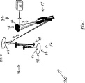
以下、図面を参照して本発明の実施の形態について詳細に説明する。本発明による投影リソグラフィー法/システムの実施の形態が図1に全体として符号20で示されている。
【0014】
本発明によれば、投影リソグラフィー法に関する発明は、照射サブシステムから発せられる遠紫外軟X線λで照射されるマスク・サブシステムを備えており、このマスク・サブシステムは、遠紫外軟X線λによって照射されたときに投影されるマスクパターンを形成するためのパターン化された反射マスクを含み、このパターン化された反射マスクは、Tiをドープされた高純度SiO2 ガラスの0.15nm以下のRa粗さを有する欠陥のない表面を覆う反射多層被膜上に被せられたパターン化された吸収テンプレートを備えたTiをドープされた高純度SiO2 ガラスウエーハを含む。
【0015】
図1の実施の形態に示されているように、投影リソグラフィー法/システム20は、パターン化された反射マスク24を含むマスク・サブシステム22を備えている。図2および図3に示されているように、パターン化された反射マスク24は、Tiをドープされた高純度SiO2 ガラスの欠陥のないウエーハ表面30を覆う反射多層被膜上に被せられたパターン化された吸収テンプレート28を備えたTiをドープされた高純度SiO2 ガラスウエーハ26を含む。反射多層被膜で覆われた、Tiをドープされた高純度SiO2 ガラスの欠陥のないウエーハ表面30は、ウエーハ表面32を覆う反射多層被膜34を備え、この反射多層被膜34は、Tiをドープされた高純度SiO2 ガラスウエーハの表面32に直接被着されていることが好ましい。図4は投影リソグラフィー法/システム20の光学的配置を示す。
【0016】
100nm未満の形状寸法を有する印刷形態の集積回路を作成するための投影リソグラフィー法は、遠紫外軟X線λを発生させかつ方向づけるための照射サブシステム36を提供する工程を含む。この照射サブシステム36は、遠紫外軟X線源38を備えている。好ましい実施の形態においては、照射サブシステム36が、集光器44によって方向づけられる遠紫外軟X線λを出力するキセノンガスプラズマを生成させる1.064μmのネオジミウムYAGレーザー40を備えている。これに代わり、遠紫外軟X線源38は、シンクロトロン、放電でポンピングされたX線レーザー、電子ビームで励起された放射線源装置、またはフェムト秒レーザーパルスによる高調波発生に基づく放射線源であってもよい。
【0017】
この投影リソグラフィー法は、照射サブシステム36から発せられる遠紫外軟X線λによって照射されるマスク・サブシステム22を提供する工程を含む。このマスク・サブシステム22を提供する工程は、遠紫外軟X線λによって照射されたときに投影されるマスクパターンを形成するためのパターン化された反射マスク24を提供する工程を含む。反射マスク24を提供することは、Tiをドープされた高純度SiO2 ガラスの欠陥のないウエーハ表面30を覆う反射多層被膜上に被せられパターン化された吸収テンプレート28を備えたTiをドープされた高純度SiO2 ガラスウエーハ26を提供する工程を含む。Tiをドープされた高純度SiO2 ガラスの欠陥のないウエーハ表面30は0.15nm以下のRa粗さを有する。Tiをドープされた高純度SiO2 ガラスウエーハ26は、欠陥を含んでおらず、Ra粗さが0.15nm以下の平滑な平面状の表面を有し、マスクによって反射される遠紫外軟X線λの散乱を阻止する。このようなRa粗さは、本発明によって表面を仕上げ、かつ原子間力顕微鏡(AFM)を用いて測定することによって得られる。図5A,5Bは、AFM測定によって測定された、0.15nm以下のRa粗さを有するTiをドープされた高純度SiO2 ガラスウエーハの表面のAFM顕微鏡写真である。
【0018】
本発明の方法は、投影サブシステム46と、放射線に感応し得るウエーハ表面50を備えた集積回路ウエーハ48とを提供する工程を含み、上記投影サブシステム46は、マスク24から投影されるマスクパターンを放射線感応性ウエーハ表面50に投影する。この投影サブシステム46は、図1および図4に示されているような4枚の直列ミラーであることが好ましく、これらミラーM1〜M4により、マスクパターンのサイズが縮小され、この縮小されたパターンが1/4の縮小率をもってウエーハ表面50に投影される。
【0019】
好ましい実施の形態においては、遠紫外軟X線λの波長は、約5nmから約15nmまでの範囲内にあり、最も好ましい照射サブシステム36は、約13.4nmを中心とする遠紫外軟X線を、13.4nmにおいて少なくとも65%の反射率を有する反射マスク24に向ける。
【0020】
提供された、Tiをドープされた高純度SiO2 ガラスウエーハ26は、欠陥を含んでおらず、すなわちガラス体にバルクガラス欠陥がなく、ガラス内に空所およびガス入り空所のような混入異物がなく、そして特に、寸法が80nmよりも大きい欠陥がないものである。特に好ましい実施の形態においては、ガラスウエーハ表面32が0.15nm以下のRa粗さを有する平面状表面となるように研磨による仕上げ加工が施された、エッチングされていないガラス表面である。TiをドープされたSiO2 ガラスからなるウエーハ26は、実質的に遠紫外軟X線λに対し不透過性であり、反射性被膜で覆われたウエーハ表面30および極めて低い粗さを有するウエーハ表面32は、本発明において、照射放射線の散乱を阻止し、かつ投影リソグラフィー工程中において極めて安定な高品質画像をウエーハ表面50上に提供する。提供されたTiをドープされた高純度SiO2 ガラスは、塩素を含まないことが好ましく、かつアルカリ金属およびアルカリ土類金属からなる不純物のレベルが10ppb未満であることが好ましい。Tiをドープされた高純度SiO2 ガラスは、5ないし10重量%のTiO2 を含み、かつ20℃における熱膨脹係数が+30ppbから−30ppbまでの範囲内にあることが好ましく、20℃における熱膨脹係数が+10ppbから−10ppbまでの範囲内にあることがさらに好ましい。ウエーハ26は、25℃における熱伝導率Kが1.40w/(m.℃)以下であることが好ましく、1.25から1.38までの範囲内にあることがさらに好ましく、約1.31が最も好ましい。
【0021】
投影リソグラフィーの間、ウエーハ26は遠紫外軟X線λの照射によって加熱されるが、このようにウエーハが加熱された場合でも、パターン化された吸収テンプレートの寸法は実質的に影響を受けず、投影された画像の変動が阻止されて投影された画像の品質が維持される。本発明の方法において、Tiをドープされた高純度SiO2 ガラスウエーハ26は、遠紫外軟X線λの照射によって動作温度にまで熱せられるが、ガラスウエーハは、このような動作温度において熱膨脹係数が略ゼロ中心になるようにTiドーパントのレベルが調整されることが好ましい。このような熱伝導率および熱膨脹係数を備えたウエーハ26は、適正な動作と安定性とを提供し、かつマスク・サブシステム22の冷却を必要としない極めて信頼性および経済性の高いリソグラフィー法/システムを提供する。好ましい実施の形態においては、マスク24およびウエーハ26は積極的には冷却されておらず、循環冷却液、熱電冷却手段、またはその他の温度上昇防止手段のような冷却システムを備えていない。
【0022】
提供された、Tiをドープされた高純度SiO2 ガラスの欠陥のないウエーハ表面32は、80nmを超える寸法を有する印刷可能な表面欠陥のない仕上げ加工された平面状表面を備えた仕上げ加工された平面状表面を有する。この仕上げ加工された平面状表面は、マスクの仕上げられた表面がウエーハ表面50上に印刷される画像を汚染しないように、ウエーハ表面50上の最小印刷寸法の1/5よりも大きい寸法の印刷可能な表面欠陥を有しないことが好ましい。Tiをドープされた高純度SiO2 ガラスの表面30に施された反射多層被膜は、この反射多層被膜を照射する遠紫外軟X線λの少なくとも65%を反射させるのが好ましく、少なくとも70%を反射させるのがさらに好ましい。好ましい実施の形態においては、ウエーハ表面32がエッチングされてなく、かつ中間のバリア層またはリリース層は設けられずに、反射多層被膜34が直接ウエーハ表面に接着されるようになっている。
【0023】
本発明はさらに、投影リソグラフィーシステムの作成方法および投影リソグラフィーパターンの投影方法を含み、この方法は、遠紫外軟X線源38を備えた照射サブシステム36を提供し、かつマスク・サブシステム22を提供する各工程を含み、マスク・サブシステム22は、マスク受容体52およびこのマスク受容体52に受容された反射マスク24を備え、反射マスク24は、受ける遠紫外軟X線の少なくとも65%を反射し得る反射多層被膜34で覆われた0.15nm以下のRa粗さを有するエッチングされていないガラスマスクウエーハ表面32を備えたTiをドープされた高純度SiO2 ガラスマスクウエーハ26を含む。この方法はさらに、焦点深度が1μm以上で開口数NAが0.1以下のカメラ54を備えた投影サブシステム46を提供し、放射線感応性印刷媒体58を備えた放射線感応性印刷サブシステム56を提供し、かつ遠紫外軟X線源38からの遠紫外軟X線が反射マスク24を照射し、反射マスク24が遠紫外軟X線を反射してテンプレート28の印刷パターンを形成し、この印刷パターンが投影サブシステムのカメラ54によって縮小されて放射線感応性印刷媒体58上に投影されるように、照射サブシステム36、マスク・サブシステム22、投影サブシステム46、および放射線感応性印刷サブシステム56を整合させる各工程を含む。
【0024】
この方法はさらに、放射線感応性印刷媒体58上に印刷され得る混入異物や表面欠陥のない表面を備えたTiをドープされた高純度SiO2 ガラスマスクウエーハ26を備えた反射マスク24を提供する工程を含む。この反射マスク24を提供する工程は、プリフォーム表面を備えかつ混入異物のないTiをドープされた高純度SiO2 ガラスマスクウエーハプリフォームを提供し、かつこのプリフォーム表面を、本発明に従って0.15nm以下のRa粗さを有する平面状マスクウエーハ表面に仕上げる各工程を含む。
【0025】
この方法は、システム20の動作中に照射サブシステム36から照射を受けたときの反射マスク24の動作温度を測定する工程と、測定された動作温度において略ゼロを中心とする熱膨脹係数を有するTiをドープされた高純度SiO2 ガラスマスクウエーハを提供する工程とを含むことが好ましい。このような熱膨脹係数の調整は、0ないし9.0重量%のTiO2 を含む高純度SiO2 ガラスの熱膨脹特性を示す図8に示されているように、SiO2 中のTiドーパントの含有率の変化を調節することによってなされる。
【0026】
この方法のさらなる実施の形態において、Tiをドープされた高純度SiO2 ガラスマスクウエーハが遠紫外軟X線により高い温度領域まで加熱され、Tiをドープされた高純度SiO2 ガラスが上記高い温度領域に対し10ppb未満で−10ppbよりも大きい熱膨脹係数を有する。この方法は、熱伝導率Kが1.40w/(m.℃)以下、さらに好ましくは1.25から1.38までの範囲、最も好ましくは約1.31の熱絶縁体(熱伝導率が低い)であるマスク24およびウエーハ26を提供し、かつウエーハ26を積極的に冷却することなくウエーハ26の温度上昇を許容する各工程を含むことが好ましい。
【0027】
本発明はさらに、プリフォーム表面を備えかつ混入異物のないTiをドープされた高純度SiO2 ガラスプリフォームを提供し、このプリフォームの表面を0.15nm以下のRa粗さを有する平面状マスク表面32に仕上加工し、この仕上げ加工された0.15nm以下のRa粗さを有する平面状マスク表面を反射多層被膜34で覆って、遠紫外軟X線に対し少なくとも65%の反射率を備えた反射マスク表面30を形成する各工程を含む遠紫外軟X線反射投影リソグラフィーマスク24の作成方法を含む。この方法はさらに、パターン化された吸収テンプレート28を反射マスク表面30上に形成する工程を含む。反射多層被膜で覆う工程は、Mo/SiまたはMo/Beのような第1素子および第2素子からなる平滑な薄層(厚さ4nm以下)を交互に形成する工程を含むことが好ましい。
【0028】
上記交互層は、13.4nmを中心とすることが好ましい最大遠紫外軟X線反射率を提供する。このような交互の反射多層被膜は、各境界で反射されるフォトンの構造的干渉に対し理想的な層の厚さと、多数の境界が被膜の反射率に寄与する最小の吸収とによって、四分の一波長板に類似した機能を有する。層間の厚さの偏差は0.01nm以内であることが好ましい。好ましい実施の形態においては、被膜が厚さ約2.8nmのMo層と、厚さ約4.0nmのSi層との81層の交互層からなる。適切な堆積条件をもってすれば、上記のような交互層で13.4nmにおいて68%以上の反射率が得られる。Mo層とSi層とからなる81層の交互層は、通常の大気にさらされたときのMoの酸化を防止するために、厚さ4nmのSi層からなることが好ましいキャップ層でカバーされていることが好ましい。マスク24の反射性被膜34は、次に反射性被膜の上面に堆積された吸収層のパターンを形成するウエーハ処理工程を用いてパターン化される。
【0029】
上記吸収層は、Al,Tiまたはその他の遠紫外軟X線吸収元素のような遠紫外軟X線吸収元素からなり、露光工程または電子ビーム直接書込み工程のようなウエーハ処理工程によってパターン化された吸収層28を形成する。好ましい実施の形態においては、反射多層被膜による被覆およびパターン化されたテンプレートの形成は、0.15nm以下のRa粗さを有するTiをドープされた高純度SiO2 ガラスウエーハの表面への多層被膜の堆積と、次の反射多層被膜の上面へのバッファ層の堆積と、次のバッファ層の上面への吸収体の堆積と、次のパターン生成リソグラフィーと、次の上記吸収体へのパターンの転写と、次のバッファ層のエッチングによる除去とにより、パターン化された反射被膜を得ることを含み、この反射被膜は遠紫外軟X線に対し好ましくは13.4nmを中心として少なくとも65%の反射率を有する。
【0030】
好ましい実施の形態においては、上記反射多層被膜は、Tiをドープされた高純度SiO2 ガラスウエーハの表面に直接堆積される。仕上げ加工された表面とTiをドープされた高純度SiO2 ガラスの特性とによって、ガラス表面と反射多層被膜との間の直接的堆積と接着とが、間接的被膜付けの複雑さを伴うことなしに、かつガラス・セラミック結晶を含む基板材料に用いられる被膜平滑化処理のような基板表面の付加的処理を必要とすることなしに提供され、ガラス表面と反射多層被膜との間の中間層が必要なくなる。仕上げ加工されたTiをドープされた高純度SiO2 ガラスウエーハの表面と反射多層被膜との間での直接的接着による接触により、優れたかつ安定な反射マスクを得ることができる。
【0031】
図6に示されているようなTiをドープされた高純度SiO2 ガラスプリフォームを提供する工程は、高純度Siを含む原料114および高純度Tiを含む原料126を提供し、高純度Siを含む原料114および高純度Tiを含む原料126を転化サイト100に配送し、これら配送された原料をTiをドープされたSiO2 スート101に転化させ、このスート101を、耐火性ジルコン炉内で回転するジルコン製採集カップ142内の高温のTiをドープされた高純度SiO2 ガラス体144の上部ガラス表面上に堆積し、スートの堆積と同時に、TiをドープされたSiO2 スートを固結させて、混入異物を含まない均質なTiをドープされた高純度SiO2 ガラス体144を得る各工程を含むことが好ましい。高純度Siを含む原料114および高純度Tiを含む原料126を提供する工程は、塩素を含まない高純度Si含有原料を提供し、かつ塩素を含まない高純度Ti含有原料を提供し、これら塩素を含まない高純度原料を塩素を含まないTiをドープされた高純度SiO2 スートに転化させ、このスートをTiをドープされた高純度SiO2 ガラスに固結させる各工程を含むことが好ましい。Si原料として好ましいのはポリメチルシロキサン、より好ましいのはポリメチルシクロシロキサン、最も好ましいのは高純度オクタメチルシクロテトラシロキサン(少なくとも99%のオクタメチルシクロテトラシロキサンからなるSi原料)のようなシロキサンが好ましい。Ti原料としてはチタニウムアルコキシドが好ましく、チタニウムイソプロポキシド[Ti(OPri)4]がより好ましく、少なくとも99%のチタニウムイソプロポキシドからなるTi原料が好ましい。窒素からなる不活性キャリアガス116がSi原料およびTi原料中に気泡として注入され、飽和を防止すべく、窒素からなる不活性キャリアガス118が、Si蒸気とキャリアガスとの混合ガスおよびTi蒸気とキャリアガスとの混合ガスに添加されて、配送システム120およびマニフォルド122を通じた原料の転化サイト100への配送を容易にしている。Si原料はマニフォルド122内でTi原料と混合されて、TiをドープされたSiO2 の均質なガス状の先駆混合物を形成することが好ましく、このガス状の先駆混合物は、炉140の上部138に取り付けられて転化サイトバーナー火炎137を生成させる転化サイトバーナー136に導管134を通じて配送され、原料混合物がTiをドープされたSiO2 スートに転化され、次いで均質なTiをドープされたSiO2 ガラスに転化される。SiO2 中のTiO2 含有量の重量%は、スート101およびガラス144内に混入させる転化サイト100に配送されるTi原料の量を変えることによって調整される。好ましい方法では、ガラス144およびプリフォーム60のTiドーパントの重量%レベルは、マスクを備えたウエーハ26の動作温度における熱膨脹係数がゼロに近付くように調整される。図8によれば、高純度SiO2 ガラス中のTiO2 の重量%の調整により、得られたガラスウエーハの熱膨脹特性が調整される。ガラスのTiドーパントの重量%は、好ましくは約6重量%のTiO2 から約9重量%のTiO2 までの範囲内、最も好ましいのは7から8重量%までの範囲内に調節される。転化サイトバーナー火炎137は、約1600℃以上の温度において原料を燃焼させ、酸化させてスートに転化させ、かつスートをガラス144に固結させるための燃料/酸素混合物(天然ガスおよび/またはH2 と酸素)で形成される。原料およびスート101の流れを阻害しかつガラス144の製造工程を複雑にする可能性のある火炎137に達する以前での反応を阻止すべく、導管134および導管中を流れる原料の温度が調節され監視されることが好ましい。炉140および特にジルコンカップおよび上方部分138は、アルカリ金属およびアルカリ土類金属、および炉から拡散してガラス144を汚染するおそれのあるその他の不純物を含まない高純度耐火煉瓦で造られていることが好ましい。このような高純度煉瓦は、高純度材料を用いかつ煉瓦を焼成して不純物を取り除くことによって得られる。
【0032】
カップ142は、ガラス体144が少なくとも0.5m、好ましくは1mの直径、少なくとも8cm、好ましくは少なくとも10cmの高さを有する円柱体であって、好ましい高さが12ないし16cmの範囲内にある円柱体となるように、直径少なくとも0.5m、より好ましくは少なくとも1mの円形体であることが好ましい。ガラス体144をTiをドープされた高純度SiO2 ガラスプリフォーム60に形成するためには、混入異物のようなガラス欠陥の存否を検査し、図7Aに示すように、ガラス体144の部分62のような欠陥のない部分を精選し、図7Bに示すように、欠陥のない部分62を切り出す作業を含むことが好ましい。次に図7Cに示すように、切り出された欠陥のない部分62から複数枚のプリフォーム60が形成される。プリフォーム60は、ガラス体144の中心部分の孔開けで部分62を切り出し、この切り出された部分62を、平面状上面64と平面状底面66とを備えた複数枚の適当なサイズの平板状プリフォーム60に切断し、この平板状プリフォーム60を、0.15nm以下の粗さを有する平面状マスクウエーハ表面を備えたマスクウエーハに仕上げるのを可能にする。平板状プリフォーム60は、図7Eに示すように、プリフォーム60の面を研磨することによって仕上げられる。プリフォーム60の上面と底面との双方が研磨ホイール68によって研磨されてウエーハ26にされるのが好ましい。プリフォーム60を研磨してウエーハ26にするには少なくとも二つの研磨工程を経ることが好ましい、プリフォーム60は、先ず粗さ約0.6ないし1.0nmの範囲のプリフォーム表面を有するように研磨され、次いでこのプリフォーム表面が粗さ0.15nm以下のマスクウエーハ表面を有するように研磨されるのが好ましい。この研磨は、液状媒体(溶液)内にこの溶液が澄まないように粒子が精細に分布されたコロイド粒子で研磨することを含むことが好ましい。全ての粒子の粒径が0.5μm未満で、全粒子が粒径分布は0.5μm未満であり、かつ球形で100nm未満、好ましくは20ないし50nmの範囲の粒径を有することが好ましい。上記コロイド粒子としては、シリカ、チタニア、アルミナまたはセリアが好ましい。本発明は、コロイドシリカ、好ましくはチタンをドープされたコロイドシリカで研磨することを含むのが最も好ましい。
【0033】
図7Eに示すように、本発明の研磨工程は、上面64と反対側の底面66とを同時に研磨することよりなる。研磨ホイール68は、合成ポリマーで形成された研磨ホイールパッドを備えているのが好ましく、この研磨ホイール表面および研磨剤の回転運動により、プリフォーム表面64および66の部分が化学的および物理的機械的の組合せで取り除かれて、反射多層被膜が堆積される仕上げられた平滑な表面が提供される。この仕上げ加工は、酸化セリウム研磨剤と硬質ポリウレタンパッドを用いてプリフォーム表面を研磨し、次いで酸化セリウム研磨剤と起毛軟質ポリウレタンパッドを用いて研磨し、次いでコロイドシリカと軟質ポリウレタンパッドを用いて研磨することを含むことが好ましい。好ましい他の実施の形態では、コロイドシリカにチタンがドープされている。仕上げ加工は、少なくとも一種類の金属酸化物の水溶液で研磨し、次いでコロイドシリカのアルカリ水溶液で研磨することを含むことが好ましい。このような研磨剤で研磨された後、プリフォーム表面は洗浄されて研磨剤が除かれ、清浄にされたウエーハ26が提供される。コロイドシリカのアルカリ水性溶液は、pHが8ないし12の範囲内、好ましくは10ないし12の範囲内、最も好ましいのは11ないし12の範囲内となるように緩衝液で調製されることが好ましい。アルカリ水溶液中のコロイドシリカは、アルカリ水溶液による表面腐食を物理的作用を通じて取り除き、かつTiをドープされたSiO2 ガラス上に頻繁に形成される水和層を取り除く。
【0034】
本発明はさらに、遠紫外軟X線反射マスクウエーハ26を含む。ウエーハは、エッチングされていない研磨された平面状第1表面32と反対側の研磨された平面状第2表面31とを備え、第1表面が80nmよりも大きい寸法の印刷可能な表面欠陥を有さずかつ0.15nm以下のRa粗さを有する混入異物を含まないTiをドープされたSiO2 ガラスウエーハからなる。図5Aおよび図5Bは、このような研磨された、混入異物を含まないTiをドープされたSiO2 ガラスウエーハ表面を示す。反対側の第2表面31もまた、80nmよりも大きい寸法の印刷可能な表面欠陥を有さずかつ0.15nm以下のRa粗さを有することが好ましい。第1表面と第2表面との間の厚さ寸法は少なくとも1mm、より好ましくは少なくとも5mm、最も好ましいのは6ないし12mm、さらに好ましいのは6ないし8mmである。混入異物を含まないTiをドープされたSiO2 ガラスマスクウエーハは塩素を含まず、アルカリ金属およびアルカリ土類金属からなる不純物レベルが10ppb未満であることが好ましい。
【0035】
本発明はまた、遠紫外軟X線反射マスクウエーハの作成方法を含み、この方法は、第1プリフォーム表面64および第2プリフォーム表面66を備えた混入異物を含まないTiをドープされた高純度SiO2 ガラスプリフォーム60を提供し、プリフォーム表面64を0.15nm以下のRa粗さを有する平面状マスクウエーハ表面に仕上げることからなる。Tiをドープされた高純度SiO2 ガラスプリフォームを提供することは、高純度Siを含有する原料114および高純度Tiを含有する原料126を提供し、原料114および126を転化サイト100に配送し、原料114および126をTiをドープされたSiO2 スート101に転化させ、スート101を混入異物を含まない均質なTiをドープされた高純度SiO2 ガラスに固結させ、このガラスをTiをドープされた高純度SiO2 ガラスプリフォーム60に形成することを含むことが好ましい。スート101およびガラス144を塩素を含まないものにするために、Si原料114およびTi原料126は塩素を含んでいないことが好ましい。第1プリフォーム表面64を平面状マスクウエーハ表面に仕上げることは、表面64を0.6nmから1.0nmまでの範囲の表面Ra粗さを有する第1の研磨されたプリフォーム表面に研磨し、次いで上記研磨されたプリフォーム表面を0.15nm以下のRa粗さを有する平面状マスクウエーハ表面に研磨することを含むことが好ましい。上記研磨工程はコロイドシリカで研磨することを含むことが好ましい。好ましい実施の形態においては、コロイドシリカが、4ないし10重量%の濃度のチタニアをドープされていることが好ましい。最も好ましい実施の形態においては、この方法は、反対側の第2プリフォーム表面66も第1プリフォーム表面64の研磨と同時に研磨することを含む。仕上げ加工は、プリフォーム表面を少なくとも一種類の金属酸化物の水溶液で研磨し、かつコロイドシリカのアルカリ溶液で表面を研磨することを含む。プリフォーム60の表面は、先ず酸化セリウム研磨剤と発泡硬質ポリウレタン合成ポリマーパッドとにより研磨され、次いで、酸化セリウム研磨剤と起毛軟質ポリウレタン合成ポリマーパッドとにより研磨されることが好ましい。好ましい実施の形態においては、コロイドシリカにはチタンがドープされている。プリフォームは、8mmを超える厚さを有し、このプリフォームが仕上げられて、6mmを超える厚さを有するウエーハ26が提供されることが好ましい。仕上げ工程では、研磨材によるプリフォーム表面の研磨に加えて、プリフォーム表面を清掃して研磨材を取り除き、反射多層被膜を接触させるための清浄な平滑表面が提供される。プリフォームを提供する工程は、遠紫外軟X線反射マスクの動作温度においてマスクウエーハがほぼゼロ中心の熱膨脹係数を有するように、Tiをドープされた高純度SiO2 ガラスプリフォームのTiドーパントの重量%のレベルを調整する工程を含むことが好ましい。
【0036】
遠紫外軟X線反射マスクウエーハを作成する本発明の方法は、100nm未満の形状寸法を有する印刷態様の集積回路の大量生産のための、遠紫外軟X線投影リソグラフィを利用することができる大量のマスクウエーハの効率的な製造に関して経済的な手段を提供するものである。さらに、Tiをドープされた高純度SiO2 ガラスウエーハ26を作成する本発明の方法は、上側の仕上げられたウエーハ表面32を検査しかつ品質認定を行なって、その表面が適正な粗さを有しかつ欠陥のないことを保証し、加えて、下側の仕上げられたウエーハ表面31を検査しかつ認定して、反対側のガラスウエーハ表面の粗さと欠陥のない性質を決定するという効果的な工程を提供する。このような検査と品質認定にはAFMが用いられることが好ましい。このことは、被膜付け、および遠紫外軟X線投影リソグラフィのためのマスクシステムの一部分として利用するためのマスクウエーハの精選および生産量を増大させる。
【0037】
パターン化された遠紫外軟X線反射マスクの使用中において、TiをドープされたSiO2 ガラスウエーハはリソグラフィー動作温度にさらされる。TiをドープされたSiO2 ガラスウエーハの動作温度には、最大動作温度が設定されている。パターン化された遠紫外軟X線反射マスクの作成中、TiをドープされたSiO2 ガラスは製造処理温度になっている。この製造処理温度は、切出し、機械加工、仕上げ、および被膜付け間の高められた温度を含む。製造処理温度は最大製造温度を含む。TiをドープされたSiO2 ガラスウエーハは耐結晶化特性を有し、結晶化が誘起される結晶化温度T結晶を有し、T結晶は最大動作温度および最大製造温度よりも実質的に高い。T結晶は最大動作温度および最大製造温度よりも少なくとも400℃高いことが好ましく。好ましくは少なくとも700℃高く、少なくとも800℃高いことが最も好ましい。最大動作温度および最大製造温度は500℃を超えることはないが、T結晶は1300℃以上であることが好ましい。TiをドープされたSiO2 ガラスでは、ガラスの結晶化がマスクの製造時および使用時に経験する高温においても結晶化が阻止される。したがって、ガラスウエーハは、それが高い結晶化温度特性を有する点で有利である。
【0038】
さらに、製造処理温度およびリソグラフィー動作温度を考慮して、TiをドープされたSiO2 ガラスは、熱循環にさらされたときにその物理的寸法を維持するようになっている。低い方の温度と高い方の温度との間の熱循環が反復されるTiをドープされたSiO2 ガラスウエーハの反射マスクの使用および製造において、ガラスウエーハの物理的寸法は実質的に不変である。TiをドープされたSiO2 ガラスは熱循環ヒステリシスに対し抵抗力を有していることが好ましく、最低リソグラフィー動作温度から最高リソグラフィー動作温度まで熱循環が反復(100回を超える)された場合にも熱循環ヒステリシスがないことが最も好ましい。0℃に近い低温から300℃に近い高温まで300℃未満の熱循環が反復された場合、ガラスウエーハの物理的寸法の測定可能な変化がないことが最も好ましい。
【0039】
好ましい実施の形態においては、TiをドープされたSiO2 ガラスは、ガラス内の永久歪みに起因する10nm/cm未満の、好ましくは2nm/cm未満の複屈折率を有する。2nm/cm未満の複屈折率は、20℃における熱膨脹率が+10ppbから−10ppbまでの範囲内、熱膨脹率の変動が10ppb未満、最も好ましくは5ppb未満となるように、SiO2 中にTiドーパントを均質に分布させることにより達成される。さらに、TiをドープされたSiO2 ガラスをアニールすることによって複屈折率を低下させることができる。TiをドープされたSiO2 ガラスは、このガラスが機械加工のような応力を受けた後に少なくとも900℃の温度で、さらに好ましくは少なくとも1000℃で、最も好ましくは1030℃でアニールされることが好ましい。
【0040】
上記のような低い複屈折率レベルの保証は、超音波をガラスに伝播させ、ガラスを通る超音波の通過時間を測定することにより、TiをドープされたSiO2 ガラスの熱膨脹を監視して、超音波の速度と、超音波にさらされたガラスの膨脹係数を決定することによって達成されることが好ましい。このようなTiをドープされたSiO2 ガラスの測定および監視は、マスク製造工程中に行なわれることが好ましい。このような超音波測定は、品質調節、検査および精選に利用されることが好ましい。このような測定は、Tiドーパントが均質に分布されたガラス体144の製造を保証することに利用されるのが好ましい。さらに、このような測定は、ガラス体144の検査と、ガラス体144から切り出される部分62の精選に用いられることが好ましい。さらにこのような測定は、仕上げ加工のような後の方の製造工程中に過度の歪みがガラス内に形成されないことを保証するのに利用され、またガラスのさらなるアニーリングが必要か否かを決定するファクターとして用いられることが好ましい。
【0041】
実施例
図5A,図5Bは、Tiをドープされた高純度SiO2 ガラスウエーハの表面のAFM顕微鏡写真を示す。図5A,図5Bは、同一ウエーハサンプルの仕上げ加工の施された表面上の離れた二つの部位を撮影したものである。混入異物を含まないTiをドープされた高純度SiO2 ガラスプリフォームに仕上げ加工を施すことによってマスクウエーハのサンプルを得た。プリフォームは、二辺が約7.6cmの正方形で厚さが約0.64cmであった。直径約152cm、厚さ(高さ)14cmのTiをドープされた高純度SiO2 ガラス円柱の混入異物を含まない領域からプリフォームを切り出すことによって、正方形のプリフォームを得た。図6にしたがって、オクタメチルシクロテトラシロキサン原料およびチタニウム・イソプロポキシド原料から、約7.5重量%のTiO2 を含む高純度SiO2 ガラスからなる上記円柱を作成した。正方形のプリフォームを、両面ラップ研磨盤を用いて平板状マスクウエーハに仕上げた。最初に7μmのアルミナ研磨剤を用いて鋳鉄板上でプリフォームの厚さ約20/1000インチ(0.0508cm)を取り除いた。次に酸化セリウム(コネチカット州、シェルトン、エンタープライズドライブ3所在のローディア社製のRodia(Rhone-Poulence)Opalinブランドの酸化セリウム)を用いて、発泡合成ポリウレタン製硬質パッド(アリゾナ州フェニックス、ワトキンズストリート、3804E.所在のローデル社製のRodel MHC−14Bブランドの発泡ポリウレタンパッド)上でプリフォームを1.5psi(0.1055kg/cm2 )と50rpmで1時間研磨した。次に、酸化セリウム(ニューヨーク州ヒックスビル、ジョンストリート、495W.所在のユニバーサルフォトニックス社製のUniversal Photonics Hastelite 919ブランドの酸化セリウム)を用いて、起毛合成ポリウレタン軟質パッド(Rodel 204Padブランドの起毛ポリウレタンパッド)上でプリフォームを1.5psi(0.1055kg/cm2 )と50rpmで20分研磨した。次に、コロイドシリカ(マサチューセッツ州ボストン、ステートストリート75所在のキャボット社製のCabot A2095ブランドのコロイドシリカ)を用いて、起毛合成ポリウレタン軟質パッド(Rodel 204Padブランドの起毛ポリウレタンパッド)上でプリフォームを1.5psi(0.1055kg/cm2 )と50rpmで5ないし10分間研磨した。次に、図5A,図5BのAFM顕微鏡写真を用いて、得られた平板状マスクウエーハを分析し、測定し、品質認定を行なった。仕上げられたTiをドープされたSiO2 ガラスウエーハの表面のRa粗さは0.15nm以下であった。好ましい実施の形態においては、本発明のTiをドープされたSiO2 ガラスウエーハの表面には欠陥がなく、Ra粗さは0.10以下、より好ましくは0.09nm、最も好ましいRa粗さは0.086nm以下であった。さらに、TiをドープされたSiO2 ガラスウエーハの表面のRMS粗さは0.15nm以下であることが好ましく、最大0.9nm以下の範囲の平均高さは0.5nm以下であった。
【0042】
本発明の精神と範囲から離れることなしに種々の変形、変更が可能であることは、当業者には明白であろう。したがって、本発明は、添付の請求項およびそれらの等価物の範囲内で提供される種々の変形、変更を含むことを意図するものである。
【図面の簡単な説明】
【図1】 本発明の一実施の形態の概略図
【図2】 本発明の一実施の形態の側断面図
【図3】 本発明の一実施の形態の平面図
【図4】 本発明の一実施の形態の概略図
【図5A】 本発明の一実施の形態のAFM顕微鏡写真
【図5B】 本発明の一実施の形態のAFM顕微鏡写真
【図6】 本発明の一実施の形態の概略図
【図7】 図7A〜図7Fは本発明の一実施の形態の製造工程図
【図8】 SiO2中のTiO2の重量%に関する温度(X軸)対熱膨脹率(Y軸)を示すグラフ
【符号の説明】
20 投影リソグラフィーシステム
22 マスク・サブシステム
24 反射マスク
26 ガラスウエーハ
28 吸収テンプレート
36 照射サブシステム
38 遠紫外軟X線源
46 投影サブシステム[0001]
Background of invention
This application is a US Provisional Patent Application No. 60/145057 “Deep UV Soft X-ray Projection Lithography Method and Mask Apparatus” filed July 22, 1999 by Claude L. Davis, Robert Sabia, Harrise J. Stevens, And US Provisional Patent Application No. 60/149840, “Deep UV Soft X-ray Projection Lithography and Mask, filed by Claude L. Davis, Kenneth E. Hrdina, Robert Sabia, Harrie J. Stevens, August 19, 1999. It is an application claiming the priority of “device”.
[0002]
Field of Invention
The present invention relates generally to projection lithography methods and systems for manufacturing integrated circuits and forming patterns having minimal geometries. In particular, the present invention relates to lithography using a deep ultraviolet soft X-ray and a reflective mask for forming a pattern image used to create a circuit pattern by reflecting the far ultraviolet soft X-ray. The present invention relates to a reflective mask that reflects far ultraviolet soft x-ray photons and enables the use of deep ultraviolet soft x-rays for lithography that exceeds the circuit forming characteristics of current optical lithography and its use It is.
[0003]
Technical background
The use of deep ultraviolet soft X-rays has the advantage of obtaining finer geometries, but due to the nature of the radiation, it is difficult to manipulate and adjust radiation at this wavelength, so in the commercial production of such radiation. Use is slow. Optical lithography systems currently used in integrated circuit manufacturing are moving toward shorter wavelengths, such as 248 nm to 193 nm and 157 nm, but hinder the commercial use and adoption of deep ultraviolet soft x-rays. It has been. One of the reasons for this slow advancement for very short wavelength radiation, such as the 15 nm band, is to make a reflective mask wafer that can withstand such radiation while maintaining a stable and high quality pattern image economically. Due to the inability to manufacture. In order to use deep ultraviolet soft X-rays in the manufacture of integrated circuits, a stable glass wafer is needed that can directly deposit a reflective coating on the surface of the glass wafer.
[0004]
As mentioned in US Pat. No. 5,698,113, current deep ultraviolet soft x-ray lithography systems are extremely expensive. In U.S. Pat. No. 5,698,113, even if etching degrades the substrate surface, the multilayer coating is covered by etching away from the substrate surface consisting of fused silica and ZERODUR type aluminosilicate glass ceramic. Attempts have been made to overcome the high prices described above by restoring the surface of the broken substrate.
[0005]
The present invention provides an economically manufactured mask wafer that is stable, directly coatable, and capable of receiving a reflective multilayer coating, and an excellent projection lithography method using deep ultraviolet soft x-rays / To provide a system. The present invention economically provides excellent mask wafer characteristics and stability without requiring reuse of the mask wafer surface, which is considered to be inferior in mask characteristics and reflectivity. The present invention provides a stable, high performance reflective mask with a reflective multilayer coating deposited directly on a finished glass surface, and a costly and complex manufacturing process, and a glass substrate surface and a reflective multilayer coating. And providing an intermediate layer between them.
[0006]
Overview of invention
One aspect of the present invention is a projection lithography method / system for producing a printed wiring-like integrated circuit having a dimension of less than 100 nm, which generates a far ultraviolet soft x-ray λ from a far ultraviolet soft x-ray source. And providing an illumination subsystem for directing the method / system. The method further includes providing a mask subsystem that is illuminated by deep ultraviolet soft x-rays λ generated from the illumination subsystem, the step of providing the mask subsystem comprising deep ultraviolet soft x-rays λ. Providing a patterned reflective mask for forming a mask pattern to be projected when irradiated by. The step of providing this patterned reflective mask includes Ti-doped SiO having a Ra roughness of 0.15 nm or less.2 Ti-doped SiO with patterned absorption template overlaid on a far-UV soft X-ray reflective multilayer coating covering a defect-free surface of glass2 Providing a glass wafer. The method further includes providing a projection subsystem and an integrated circuit wafer with a wafer surface that is sensitive to radiation, wherein the projection subsystem includes a mask projected from the patterned reflective mask pattern. Projecting a lithographic pattern onto the radiation-sensitive wafer surface.
[0007]
In another aspect, the invention includes a method of making a projection lithographic system and a projection lithography method, the method providing an illumination subsystem with a deep ultraviolet soft x-ray source and providing a mask subsystem The mask subsystem comprises a mask receiving member and a reflective mask received by the mask receiving member, the reflective mask having an unetched glass surface exposed to deep ultraviolet soft x-rays. Ti-doped high purity SiO covered with a reflective multilayer coating having a reflectivity of at least 65%2 A glass mask wafer is provided. The method further provides a projection subsystem including a camera with a depth of focus of 1 μm or more and a numerical aperture NA of 0.1 or less, and provides a radiation sensitive printing subsystem with a radiation sensitive printing medium, the illumination Including aligning the subsystem, the mask subsystem, the projection subsystem, and the radiation sensitive printing subsystem, wherein the deep ultraviolet soft x-ray source irradiates the reflective mask with far ultraviolet soft x-rays A projection pattern projected onto the radiation-sensitive print medium is formed by the camera of the projection subsystem.
[0008]
The present invention further includes a method of making a deep ultraviolet soft X-ray reflective mask, which comprises a high purity SiO doped with Ti having a preform surface and no contaminating foreign matter.2 A glass preform is provided, the surface of the preform is finished into a planar mask wafer surface having a Ra roughness of 0.15 nm or less, and the finished planar mask wafer surface is covered with a reflective multilayer coating. And each step of forming a reflective mask surface having a reflectivity of at least 65% for deep ultraviolet soft X-rays.
[0009]
The present invention is a high purity SiO doped Ti-free material with a first polished surface that has not been etched and a second polished planar surface on the opposite side that does not contain contaminants.2 Including a method for producing a far ultraviolet soft X-ray reflective mask wafer including a glass wafer, wherein the first surface has a printable surface defect having a dimension larger than 80 nm and has a Ra roughness of 0.15 nm or less. Have.
[0010]
The present invention further includes a method of making a far ultraviolet soft X-ray reflective mask wafer, the method comprising a first preform surface and a second preform surface, and doped with Ti that does not contain contaminants. SiO2 A glass preform is provided, and each step includes finishing the first preform surface into a planar mask wafer surface having a Ra roughness of 0.15 nm or less.
[0011]
Additional features and advantages of the invention will be set forth in the description which follows and will be readily apparent to those skilled in the art from the following detailed description, claims and accompanying drawings.
[0012]
Both the foregoing general description and the following detailed description are merely illustrative of the present invention and are intended to provide an overall picture for understanding the characteristics and characteristics of the present invention as recited in the claims. The accompanying drawings are included to provide a further understanding of the invention and constitute a part of this specification. The drawings show various embodiments of the present invention, and together with the description, serve to explain the principle and operation of the present invention.
[0013]
BEST MODE FOR CARRYING OUT THE INVENTION
Hereinafter, embodiments of the present invention will be described in detail with reference to the drawings. An embodiment of a projection lithography method / system according to the present invention is indicated generally at 20 in FIG.
[0014]
In accordance with the present invention, an invention relating to a projection lithography method comprises a mask subsystem that is illuminated with deep ultraviolet soft x-rays λ emitted from an illumination subsystem, the mask subsystem comprising far ultraviolet soft x-rays. a patterned reflective mask for forming a mask pattern projected when irradiated by λ, the patterned reflective mask comprising Ti-doped high purity SiO 22 Ti-doped high-purity SiO with a patterned absorption template over a reflective multilayer coating covering a defect-free surface with a Ra roughness of 0.15 nm or less of glass2 Includes glass wafers.
[0015]
As shown in the embodiment of FIG. 1, the projection lithography method /
[0016]
Projection lithography methods for creating printed form integrated circuits having geometries of less than 100 nm include providing an
[0017]
The projection lithography method includes providing a
[0018]
The method of the present invention includes the steps of providing a
[0019]
In the preferred embodiment, the wavelength of the far ultraviolet soft x-ray λ is in the range of about 5 nm to about 15 nm, and the most
[0020]
Provided high purity SiO doped with Ti2 The
[0021]
During projection lithography, the
[0022]
Provided high purity SiO doped with Ti2 Glass
[0023]
The present invention further includes a method of creating a projection lithography system and a method of projecting a projection lithography pattern, which provides an
[0024]
The method further includes Ti-doped high purity SiO with a surface free of contaminants and surface defects that can be printed on the radiation
[0025]
The method includes the steps of measuring the operating temperature of the
[0026]
In a further embodiment of this method, high purity SiO doped with Ti2 A glass mask wafer is heated to a high temperature range by far ultraviolet soft X-rays and Ti-doped high purity SiO2 The glass has a coefficient of thermal expansion of less than 10 ppb and greater than -10 ppb for the high temperature region. In this method, a thermal insulator having a thermal conductivity K of 1.40 w / (m. ° C.) or less, more preferably in the range of 1.25 to 1.38, and most preferably about 1.31 (with a thermal conductivity of Preferably, the steps include providing a
[0027]
The present invention further provides high-purity SiO doped with Ti that has a preform surface and is free of contaminants.2 A glass preform is provided, and the surface of the preform is finished into a
[0028]
The alternating layers provide maximum far ultraviolet soft x-ray reflectivity, preferably centered at 13.4 nm. Such alternating reflective multilayer coatings are divided into quadrants by the ideal layer thickness for the photon structural interference reflected at each boundary and the minimum absorption at which many boundaries contribute to the reflectivity of the coating. The function is similar to that of a single wave plate. The thickness deviation between the layers is preferably within 0.01 nm. In a preferred embodiment, the coating consists of 81 alternating layers of a Mo layer with a thickness of about 2.8 nm and a Si layer with a thickness of about 4.0 nm. With appropriate deposition conditions, a reflectivity of 68% or higher at 13.4 nm can be obtained with the alternating layers as described above. The 81 alternating layers of Mo and Si layers are covered with a cap layer, preferably a 4 nm thick Si layer, to prevent oxidation of Mo when exposed to normal air. Preferably it is. The reflective coating 34 of the
[0029]
The absorption layer is made of a far ultraviolet soft X-ray absorbing element such as Al, Ti or other far ultraviolet soft X-ray absorbing element, and is patterned by a wafer processing process such as an exposure process or an electron beam direct writing process. The absorption layer 28 is formed. In a preferred embodiment, the coating with the reflective multilayer coating and the formation of the patterned template are Ti-doped high-purity SiO having a Ra roughness of 0.15 nm or less.2 Deposition of the multilayer coating on the surface of the glass wafer, deposition of the buffer layer on the top of the next reflective multilayer coating, deposition of the absorber on the top of the next buffer layer, the next pattern generation lithography, Transfer of the pattern to the absorber and subsequent removal of the buffer layer by etching to obtain a patterned reflective coating, which preferably has a thickness of 13.4 nm for deep ultraviolet soft X-rays. It has a reflectivity of at least 65% as the center.
[0030]
In a preferred embodiment, the reflective multilayer coating comprises Ti-doped high-purity SiO.2 Deposited directly on the surface of the glass wafer. Finished surface and Ti-doped high purity SiO2 Depending on the properties of the glass, the direct deposition and adhesion between the glass surface and the reflective multilayer coating does not involve the complexity of indirect coating, and the coating used for substrate materials including glass-ceramic crystals It is provided without the need for additional processing of the substrate surface, such as a smoothing process, eliminating the need for an intermediate layer between the glass surface and the reflective multilayer coating. Finished Ti-doped high purity SiO2 An excellent and stable reflective mask can be obtained by direct contact between the surface of the glass wafer and the reflective multilayer coating.
[0031]
Ti-doped high purity SiO as shown in FIG.2 The step of providing a glass preform provides a raw material 114 containing high purity Si and a raw material 126 containing high purity Ti, and delivers the raw material 114 containing high purity Si and the raw material 126 containing high purity Ti to the
[0032]
The
[0033]
As shown in FIG. 7E, the polishing step of the present invention consists of simultaneously polishing the
[0034]
The present invention further includes a deep ultraviolet soft X-ray
[0035]
The present invention also includes a method of making a deep ultraviolet soft X-ray reflective mask wafer that includes a
[0036]
The method of the present invention for producing a far ultraviolet soft x-ray reflective mask wafer is capable of utilizing the far ultraviolet soft x-ray projection lithography for mass production of printed-circuit integrated circuits having a geometry of less than 100 nm. The present invention provides an economical means for the efficient manufacture of the mask wafers. In addition, high purity SiO doped with Ti2 The method of the present invention for making a
[0037]
Ti-doped SiO in use of patterned deep UV soft X-ray reflective mask2 Glass wafers are exposed to lithographic operating temperatures. Ti-doped SiO2 The maximum operating temperature is set as the operating temperature of the glass wafer. During the preparation of patterned deep UV soft X-ray reflective masks, Ti doped SiO2 The glass is at the manufacturing process temperature. This manufacturing process temperature includes elevated temperatures during cutting, machining, finishing, and coating. The manufacturing process temperature includes the maximum manufacturing temperature. Ti-doped SiO2 The glass wafer has a crystallization resistance property and a crystallization temperature T at which crystallization is induced.crystalAnd TcrystalIs substantially higher than the maximum operating temperature and the maximum manufacturing temperature. TcrystalIs preferably at least 400 ° C. higher than the maximum operating temperature and the maximum manufacturing temperature. Preferably it is at least 700 ° C higher and most preferably at least 800 ° C higher. Maximum operating temperature and maximum manufacturing temperature will not exceed 500 ° C, but TcrystalIs preferably 1300 ° C. or higher. Ti-doped SiO2 Glass prevents crystallization even at the high temperatures at which glass crystallization is experienced during mask manufacture and use. Thus, a glass wafer is advantageous in that it has high crystallization temperature characteristics.
[0038]
In addition, Ti doped SiO, taking into account manufacturing process temperatures and lithography operating temperatures2 Glass is designed to maintain its physical dimensions when subjected to thermal cycling. Ti-doped SiO with repeated thermal cycling between lower and higher temperatures2 In the use and manufacture of glass wafer reflective masks, the physical dimensions of the glass wafer are substantially unchanged. Ti-doped SiO2 The glass is preferably resistant to thermal cycling hysteresis, and there is no thermal cycling hysteresis even when thermal cycling is repeated (over 100 times) from the lowest lithography operating temperature to the highest lithography operating temperature. Most preferred. Most preferably, there is no measurable change in the physical dimensions of the glass wafer when thermal cycling below 300 ° C. is repeated from a low temperature close to 0 ° C. to a high temperature close to 300 ° C.
[0039]
In a preferred embodiment, Ti doped SiO2 The glass has a birefringence of less than 10 nm / cm, preferably less than 2 nm / cm due to permanent set in the glass. The birefringence of less than 2 nm / cm is SiO 2 so that the coefficient of thermal expansion at 20 ° C. is in the range from +10 ppb to −10 ppb and the variation of the coefficient of thermal expansion is less than 10 ppb, most preferably less than 5 ppb.2 This is achieved by uniformly distributing the Ti dopant therein. Furthermore, SiO doped with Ti2 Birefringence can be lowered by annealing the glass. Ti-doped SiO2 The glass is preferably annealed at a temperature of at least 900 ° C., more preferably at least 1000 ° C., and most preferably at 1030 ° C. after the glass is subjected to stress such as machining.
[0040]
The guarantee of a low birefringence level as described above is achieved by propagating ultrasonic waves into the glass and measuring the transit time of the ultrasonic waves through the glass, so that the SiO doped with Ti.2 Preferably, this is accomplished by monitoring the thermal expansion of the glass and determining the speed of the ultrasonic wave and the coefficient of expansion of the glass exposed to the ultrasonic wave. Such Ti-doped SiO2 Glass measurement and monitoring is preferably performed during the mask manufacturing process. Such ultrasonic measurement is preferably used for quality adjustment, inspection and selection. Such a measurement is preferably used to ensure the production of a
[0041]
Example
FIGS. 5A and 5B show high purity SiO doped with Ti.2 The AFM micrograph of the surface of a glass wafer is shown. FIG. 5A and FIG. 5B are images of two distant sites on the surface of the same wafer sample that has been finished. Ti-doped high-purity SiO free from contaminating foreign matter2 A mask wafer sample was obtained by finishing the glass preform. The preform was a square with sides of about 7.6 cm and a thickness of about 0.64 cm. High-purity SiO doped with Ti having a diameter of about 152 cm and a thickness (height) of 14 cm2 A square preform was obtained by cutting the preform from an area of the glass cylinder that did not contain the contaminated foreign matter. According to FIG. 6, about 7.5 wt% TiO from the octamethylcyclotetrasiloxane raw material and the titanium isopropoxide raw material.2 High purity SiO22 The above cylinder made of glass was prepared. The square preform was finished into a flat mask wafer using a double-sided lapping polishing machine. First, a preform thickness of about 20/1000 inches (0.0508 cm) was removed on a cast iron plate using a 7 μm alumina abrasive. Next, using cerium oxide (Rodia (Rhone-Poulence) Opalin branded cerium oxide manufactured by Rhodia Co., Ltd., Shelton, Connecticut), a rigid pad made of foamed synthetic polyurethane (Wattkins Street, 3804E, Phoenix, Arizona) The preform is 1.5 psi (0.1055 kg / cm) on the Rodel MHC-14B brand polyurethane foam pad from Rodel, Inc.2 ) And 50 rpm for 1 hour. Next, using cerium oxide (Universal Photonics Hastellite 919 brand cerium oxide, manufactured by Universal Photonics, Inc., John Street, Hicksville, NY), a raised synthetic polyurethane soft pad (Rodel 204 Pad brand raised polyurethane pad) ) The preform is 1.5 psi (0.1055 kg / cm)2 And polishing at 50 rpm for 20 minutes. The preforms were then placed on a brushed synthetic polyurethane soft pad (Rodel 204 Pad brand brushed polyurethane pad) using colloidal silica (Cabot A2095 brand colloidal silica manufactured by Cabot, State Street 75, Boston, Massachusetts). .5 psi (0.1055 kg / cm2 ) And 50 rpm for 5 to 10 minutes. Next, using the AFM micrographs of FIGS. 5A and 5B, the obtained flat mask wafer was analyzed, measured, and quality certified. Finished Ti-doped SiO2 The surface roughness of the glass wafer was 0.15 nm or less. In a preferred embodiment, the Ti-doped SiO of the present invention.2 There was no defect on the surface of the glass wafer, the Ra roughness was 0.10 or less, more preferably 0.09 nm, and the most preferable Ra roughness was 0.086 nm or less. Furthermore, SiO doped with Ti2 The RMS roughness of the surface of the glass wafer is preferably 0.15 nm or less, and the average height in the range of 0.9 nm or less was 0.5 nm or less.
[0042]
It will be apparent to those skilled in the art that various modifications and variations can be made without departing from the spirit and scope of the invention. Therefore, it is intended that this invention include various modifications and changes provided within the scope of the appended claims and their equivalents.
[Brief description of the drawings]
FIG. 1 is a schematic diagram of an embodiment of the present invention.
FIG. 2 is a side sectional view of an embodiment of the present invention.
FIG. 3 is a plan view of an embodiment of the present invention.
FIG. 4 is a schematic view of an embodiment of the present invention.
FIG. 5A is an AFM micrograph of an embodiment of the present invention.
FIG. 5B is an AFM micrograph of one embodiment of the present invention.
FIG. 6 is a schematic view of an embodiment of the present invention.
7A to 7F are manufacturing process diagrams of an embodiment of the present invention.
FIG. 8 SiO2TiO in2Showing temperature (X-axis) vs. coefficient of thermal expansion (Y-axis) for weight percent
[Explanation of symbols]
20 Projection lithography system
22 Mask Subsystem
24 reflective mask
26 Glass wafer
28 Absorption Template
36 Irradiation subsystem
38 Deep UV soft X-ray source
46 Projection Subsystem
Claims (22)
遠紫外軟X線源を備えて、遠紫外軟X線λを発生させかつ方向づけるための照射サブシステムを提供し、
該照射サブシステムによって発生せしめられた前記遠紫外軟X線λによって照射されるマスク・サブシステムを提供し、
前記遠紫外軟X線λによって照射されたときに投影されるマスクリソグラフィーパターンを形成するためにパターン化された、マスク・サブシステムの反射リソグラフィーマスクを提供し、
ここで、前記パターン化された反射マスクは、TiをドープされたSiO2 ガラスウエーハを含み、前記ガラスウエーハは、0.15nm以下のRa粗さを有する欠陥のない表面を有し、前記表面を覆う遠紫外軟X線λを反射し得る多層被膜を有し、前記多層被膜上に被せられたパターン化された遠紫外軟X線λ吸収テンプレートを有してなり、
投影サブシステムを提供し、
遠紫外軟X線λに感応するウエーハ表面を備えた集積回路ウエーハを提供し、
前記投影サブシステムを用いて、前記パターン化された反射マスクから投影されるマスクパターンを放射線感応性ウエーハ表面に投影する、
各工程を含むことを特徴とする投影リソグラフィー方法。A projection lithography method for producing an integrated circuit in a printed wiring mode having a geometric dimension of less than 100 nm, comprising:
Providing an irradiation subsystem for generating and directing a deep ultraviolet soft x-ray λ, comprising a deep ultraviolet soft x-ray source;
Providing a mask subsystem illuminated by the deep ultraviolet soft X-ray λ generated by the illumination subsystem;
Providing a reflective lithographic mask of a mask subsystem patterned to form a mask lithographic pattern that is projected when irradiated by said deep ultraviolet soft x-ray λ;
Here, the patterned reflective mask includes a SiO 2 glass wafer doped with Ti, and the glass wafer has a defect-free surface having a Ra roughness of 0.15 nm or less, A multilayer coating capable of reflecting the far ultraviolet soft X-ray λ covering, and a patterned far ultraviolet soft X-ray λ absorption template covered on the multilayer coating;
Providing a projection subsystem;
Providing an integrated circuit wafer with a wafer surface sensitive to deep ultraviolet soft X-rays λ,
Projecting a mask pattern projected from the patterned reflective mask onto a radiation-sensitive wafer surface using the projection subsystem;
A projection lithography method comprising each step.
遠紫外軟X線源を備えた照射サブシステムを提供し、
マスク受容部材と、該マスク受容部材に受容された、Tiをドープされた高純度SiO2 ガラスマスクウエーハとを備えた反射マスクを含むマスク・サブシステムを提供し、ここで、前記ガラスマスクウエーハは、遠紫外軟X線に対し少なくとも65%の反射率を備えた反射多層被膜で覆われたエッチングされていないガラスマスクウエーハ表面を有し、
1μm以上の焦点深度と0.1以下の開口数NAとを備えたカメラを含む投影サブシステムを提供し、
放射線感応印刷媒体を備えた放射線感応印刷サブシステムを提供し、
前記照射サブシステム、前記マスク・サブシステム、前記投影サブシステムおよび前記放射線感応印刷サブシステムを整合させ、遠紫外軟X線源からの遠紫外軟X線で前記反射マスクを照射し、該反射マスクが前記放射線を反射させて、前記投影サブシステムのカメラによって前記放射線感応印刷媒体上に投影される印刷パターンを形成する、
各工程を含むことを特徴とする方法。A method for creating a projection lithographic printing pattern comprising:
Providing an irradiation subsystem with a deep ultraviolet soft X-ray source;
A mask-receiving member, which is received in the mask-receiving member, providing a mask subsystem including a reflective mask having a high-purity SiO 2 glass mask wafer doped with Ti, wherein said glass mask wafer An unetched glass mask wafer surface covered with a reflective multilayer coating having a reflectivity of at least 65% for deep ultraviolet soft x-rays;
Providing a projection subsystem including a camera with a depth of focus of 1 μm or more and a numerical aperture NA of 0.1 or less;
Providing a radiation-sensitive printing subsystem with radiation-sensitive printing media;
Aligning the illumination subsystem, the mask subsystem, the projection subsystem and the radiation sensitive printing subsystem, irradiating the reflective mask with far ultraviolet soft x-rays from a far ultraviolet soft x-ray source; Reflects the radiation to form a printed pattern that is projected onto the radiation-sensitive print medium by a camera of the projection subsystem;
A method comprising each step.
プリフォーム表面を備えかつ混入異物を含まないTiをドープされた高純度SiO2 ガラスプリフォームを提供し、
前記プリフォーム表面を、0.15nm以下のRa粗さを有する平面状マスクウエーハ表面に仕上げ加工し、
該0.15nm以下のRa粗さを有する仕上げられた平面状マスクウエーハ表面を反射多層被膜で覆って、遠紫外軟X線に対し少なくとも65%の反射率を有する反射マスク表面を形成する、
各工程を含むことを特徴とする方法。A method for producing a deep ultraviolet soft X-ray reflective mask,
Providing a high-purity SiO 2 glass preform doped with Ti that has a preform surface and does not contain contaminants,
The preform surface is finished into a planar mask wafer surface having a Ra roughness of 0.15 nm or less,
Covering the finished planar mask wafer surface having a Ra roughness of 0.15 nm or less with a reflective multilayer coating to form a reflective mask surface having a reflectivity of at least 65% for deep ultraviolet soft X-rays;
A method comprising each step.
第1のプリフォーム表面と第2のプリフォーム表面とを備えかつ混入異物を含まないTiをドープされたSiO2 ガラスプリフォームを提供し、
前記第1のプリフォーム表面を、0.15nm以下のRa粗さを有する平面状マスクウエーハ表面に仕上げ加工する各工程を含むものであって、
前記Tiをドープされた高純度SiO2 ガラスプリフォームを提供する工程が、高純度Siを含む原料および高純度Tiを含む原料を提供し、該高純度Siを含む原料および高純度Tiを含む原料を転化サイトに配送し、前記高純度Siを含む原料および高純度Tiを含む原料を、TiをドープされたSiO2 ガラススートに転化させ、該TiをドープされたSiO2 ガラススートを、混入異物を含まない均質なTiをドープされたSiO2 ガラスに固結させ、該ガラスを、TiをドープされたSiO2 ガラスプリフォームに成形する各工程をさらに含むものであって、前記高純度Siを含む原料および高純度Tiを含む原料を提供する工程が、塩素を含まない高純度Siを含む原料および塩素を含まない高純度Tiを含む原料を提供し、該塩素を含まない原料を、塩素を含まないTiをドープされたSiO2 ガラススートに転化させ、該スートを、塩素を含まないTiをドープされたSiO2 ガラスに固結させる各工程を含むことを特徴とする遠紫外軟X線反射マスクウエーハ作成の方法。A method for producing a deep ultraviolet soft X-ray reflective mask wafer, comprising:
Providing a Ti-doped SiO 2 glass preform comprising a first preform surface and a second preform surface and free of contaminating foreign matter;
Each step of finishing the first preform surface into a planar mask wafer surface having a Ra roughness of 0.15 nm or less,
The step of providing the Ti-doped high-purity SiO 2 glass preform provides a raw material containing high-purity Si and a raw material containing high-purity Ti, and the raw material containing the high-purity Si and the raw material containing high-purity Ti was delivered to the conversion site, a raw material containing the raw material and high purity Ti including the high-purity Si, it is converted to SiO 2 glass soot doped with Ti, the SiO 2 glass soot doped with the Ti, mixed foreign substance And further solidifying Ti-doped SiO 2 glass containing no Ti, and further forming each glass into a Ti-doped SiO 2 glass preform, the high-purity Si being Providing a raw material containing high purity Ti containing no chlorine and a raw material containing high purity Ti containing no chlorine and a step of providing a raw material containing high purity Ti containing no chlorine The raw material not containing the chlorine, is converted to SiO 2 glass soot doped with Ti containing no chlorine, the soot, to include the step of consolidating the SiO 2 glass doped with Ti containing no chlorine A method for producing a deep ultraviolet soft X-ray reflective mask wafer characterized by the following:
前記パターン化された反射マスクは、0.15nm以下のRa粗さを有するTiをドープされたSiO2 ガラスの欠陥のない表面を覆う遠紫外軟X線λを反射し得る多層被膜上に被せられたパターン化された吸収テンプレートを備えたTiをドープされたSiO2 ガラスウエーハを含み、反射多層膜を被せられたTiをドープされた欠陥のない前記ガラスウエーハ表面が、80nmより大きな欠陥を有しないことを特徴とするマスクウエーハ。A non-crystallized Ti-doped far-UV soft X-ray reflective lithography mask wafer containing no contaminating foreign material, wherein the Ti-doped SiO 2 glass wafer contains 5 to 10% by weight of TiO 2 The alkali metal and alkaline earth metal have a content of 10 ppb or less, a thermal expansion coefficient in the range from +10 ppb to −10 ppb at 20 ° C., and a thermal expansion coefficient distribution of 15 ppb or less.
The patterned reflective mask is overlaid on a multilayer coating capable of reflecting deep ultraviolet soft X-rays λ covering a defect-free surface of Ti-doped SiO 2 glass having a Ra roughness of 0.15 nm or less. Including a Ti-doped SiO 2 glass wafer with a patterned absorption template, and the Ti-doped defect-free glass wafer surface covered with a reflective multilayer is free of defects larger than 80 nm A mask wafer characterized by that.
5ないし10重量%のTiO2 を含み、アルカリ金属およびアルカリ土類金属については、含有量が10ppb以下であって、かつ20℃において+10ppbから−10ppbまでの範囲の熱膨脹係数を有し、熱膨張係数の分布が15ppb以下であって、混入のないTiをドープされたガラスプリフォームであって、第1のプリフォーム表面を有するものを準備する工程、
前記第1のプリフォーム表面を平面状マスクウエーハ表面に仕上げる工程が、前記第1のプリフォーム表面を研磨して、第1の研磨されたプリフォーム表面であって、0.6ないし1.0nmRa粗さを有するものにし、
さらに、前記研磨された表面を、コロイドシリカで研磨して、0.15nm以下のRa粗さを有する欠陥のない平面マスクウエーハ表面にする工程を含むことを特徴とする方法。A method for producing a deep ultraviolet soft X-ray reflective mask wafer, comprising:
Containing 5 to 10% by weight TiO 2 , for alkali metals and alkaline earth metals, the content is less than 10 ppb and has a coefficient of thermal expansion in the range from +10 ppb to −10 ppb at 20 ° C. Preparing a glass preform having a coefficient distribution of not more than 15 ppb and doped with Ti without contamination and having a first preform surface;
The step of finishing the first preform surface into a planar mask wafer surface comprises polishing the first preform surface to obtain a first polished preform surface having a roughness of 0.6 to 1.0 nmRa. To have
The method further comprises the step of polishing the polished surface with colloidal silica to a defect-free planar mask wafer surface having a Ra roughness of 0.15 nm or less.
Applications Claiming Priority (5)
| Application Number | Priority Date | Filing Date | Title |
|---|---|---|---|
| US14505799P | 1999-07-22 | 1999-07-22 | |
| US60/145,057 | 1999-07-22 | ||
| US14984099P | 1999-08-19 | 1999-08-19 | |
| US60/149,840 | 1999-08-19 | ||
| PCT/US2000/019060 WO2001007967A1 (en) | 1999-07-22 | 2000-07-13 | Extreme ultraviolet soft x-ray projection lithographic method and mask devices |
Publications (3)
| Publication Number | Publication Date |
|---|---|
| JP2003505891A JP2003505891A (en) | 2003-02-12 |
| JP2003505891A5 JP2003505891A5 (en) | 2006-01-05 |
| JP3770542B2 true JP3770542B2 (en) | 2006-04-26 |
Family
ID=26842619
Family Applications (1)
| Application Number | Title | Priority Date | Filing Date |
|---|---|---|---|
| JP2001512998A Expired - Lifetime JP3770542B2 (en) | 1999-07-22 | 2000-07-13 | Deep ultraviolet soft X-ray projection lithography method and mask apparatus |
Country Status (6)
| Country | Link |
|---|---|
| US (2) | US6465272B1 (en) |
| EP (1) | EP1218796A4 (en) |
| JP (1) | JP3770542B2 (en) |
| KR (1) | KR100647968B1 (en) |
| AU (1) | AU5932500A (en) |
| WO (1) | WO2001007967A1 (en) |
Families Citing this family (65)
| Publication number | Priority date | Publication date | Assignee | Title |
|---|---|---|---|---|
| US7364072B1 (en) | 1996-01-02 | 2008-04-29 | Steven Jerome Moore | Apparatus and method for security |
| US6396067B1 (en) * | 1998-05-06 | 2002-05-28 | Koninklijke Philips Electronics N.V. | Mirror projection system for a scanning lithographic projection apparatus, and lithographic apparatus comprising such a system |
| JP3766802B2 (en) | 1999-07-22 | 2006-04-19 | コーニング インコーポレイテッド | Far-UV soft X-ray projection lithography system and lithography element |
| US6776006B2 (en) | 2000-10-13 | 2004-08-17 | Corning Incorporated | Method to avoid striae in EUV lithography mirrors |
| US8047023B2 (en) | 2001-04-27 | 2011-11-01 | Corning Incorporated | Method for producing titania-doped fused silica glass |
| US20030064161A1 (en) * | 2001-06-06 | 2003-04-03 | Malinowski Michael E. | Method for reducing carbon contamination of multilayer mirrors |
| DE10139188A1 (en) * | 2001-08-16 | 2003-03-06 | Schott Glas | Glass ceramic for X-ray optical components |
| US6818357B2 (en) * | 2001-10-03 | 2004-11-16 | Intel Corporation | Photolithographic mask fabrication |
| US6997015B2 (en) | 2001-11-27 | 2006-02-14 | Corning Incorporated | EUV lithography glass structures formed by extrusion consolidation process |
| US6988377B2 (en) | 2001-11-27 | 2006-01-24 | Corning Incorporated | Method for making extreme ultraviolet lithography structures |
| CN1282039C (en) * | 2001-12-04 | 2006-10-25 | Asml荷兰有限公司 | Lithographic apparatus, device manufacturing method, and method of manufacturing an optical element |
| US6829908B2 (en) | 2002-02-27 | 2004-12-14 | Corning Incorporated | Fabrication of inclusion free homogeneous glasses |
| US6832493B2 (en) | 2002-02-27 | 2004-12-21 | Corning Incorporated | High purity glass bodies formed by zero shrinkage casting |
| US7053017B2 (en) | 2002-03-05 | 2006-05-30 | Corning Incorporated | Reduced striae extreme ultraviolet elements |
| US7129010B2 (en) * | 2002-08-02 | 2006-10-31 | Schott Ag | Substrates for in particular microlithography |
| US6975385B2 (en) * | 2002-11-08 | 2005-12-13 | Canon Kabushiki Kaisha | Projection optical system and exposure apparatus |
| US6885015B2 (en) * | 2002-12-30 | 2005-04-26 | Intel Corporation | Thermionic-cathode for pre-ionization of an extreme ultraviolet (EUV) source supply |
| US6953532B2 (en) * | 2003-03-06 | 2005-10-11 | Cabot Microelectronics Corporation | Method of polishing a lanthanide substrate |
| US7691279B2 (en) * | 2003-03-27 | 2010-04-06 | Hoya Corporation | Method of producing a glass substrate for a mask blank and method of producing a mask blank |
| JP4792706B2 (en) * | 2003-04-03 | 2011-10-12 | 旭硝子株式会社 | Silica glass containing TiO2 and method for producing the same |
| JP5367204B2 (en) * | 2003-04-03 | 2013-12-11 | 旭硝子株式会社 | Silica glass containing TiO2 and optical member for EUV lithography |
| JP2010275189A (en) * | 2003-04-03 | 2010-12-09 | Asahi Glass Co Ltd | SILICA GLASS CONTAINING TiO2 AND OPTICAL MEMBER FOR EUV LITHOGRAPHY |
| JP5402975B2 (en) * | 2003-04-03 | 2014-01-29 | 旭硝子株式会社 | Silica glass containing TiO2 and method for producing the same |
| JP4792705B2 (en) * | 2003-04-03 | 2011-10-12 | 旭硝子株式会社 | Silica glass containing TiO2 and method for producing the same |
| JP2011168485A (en) * | 2003-04-03 | 2011-09-01 | Asahi Glass Co Ltd | SILICA GLASS CONTAINING TiO2 AND METHOD OF PRODUCING THE SAME |
| AU2003229725A1 (en) * | 2003-04-24 | 2004-11-19 | Carl Zeiss Smt Ag | Projection optical system |
| DE10319596A1 (en) * | 2003-05-02 | 2004-11-25 | Degussa Ag | Multicomponent glass |
| JP4402656B2 (en) | 2003-09-17 | 2010-01-20 | カール・ツァイス・エスエムティー・アーゲー | Mask and lithographic apparatus |
| JP2005109158A (en) * | 2003-09-30 | 2005-04-21 | Canon Inc | Cooling apparatus and method therefor, aligner equipped therewith, and manufacturing method of device |
| DE10359102A1 (en) * | 2003-12-17 | 2005-07-21 | Carl Zeiss Smt Ag | Optical component comprises a material with a longitudinal expansion coefficient which is spatially dependent |
| JP4492123B2 (en) * | 2004-01-05 | 2010-06-30 | 旭硝子株式会社 | Silica glass |
| US7164200B2 (en) * | 2004-02-27 | 2007-01-16 | Agere Systems Inc. | Techniques for reducing bowing in power transistor devices |
| JP2005333124A (en) * | 2004-04-22 | 2005-12-02 | Asahi Glass Co Ltd | Low expansion glass substrate for reflection type mask and reflection type mask |
| EP1738224A1 (en) * | 2004-04-22 | 2007-01-03 | Asahi Glass Company, Limited | Low-expansion glass substrate for a reflective mask and reflective mask |
| JP4665443B2 (en) | 2004-06-22 | 2011-04-06 | 旭硝子株式会社 | Glass substrate polishing method |
| US7230695B2 (en) * | 2004-07-08 | 2007-06-12 | Asahi Glass Company, Ltd. | Defect repair device and defect repair method |
| US7586059B2 (en) * | 2004-08-27 | 2009-09-08 | Infineon Technologies Ag | Lithography mask substrate labeling system |
| US20060179879A1 (en) * | 2004-12-29 | 2006-08-17 | Ellison Adam J G | Adjusting expansivity in doped silica glasses |
| EP1843985B1 (en) | 2005-02-02 | 2012-06-06 | Asahi Glass Company, Limited | Process for polishing glass substrate |
| SG124407A1 (en) * | 2005-02-03 | 2006-08-30 | Asml Netherlands Bv | Method of generating a photolithography patterningdevice, computer program, patterning device, meth od of determining the position of a target image on or proximate a substrate, measurement device, and lithographic apparatus |
| WO2006135098A1 (en) * | 2005-06-14 | 2006-12-21 | Asahi Glass Co., Ltd. | Method of finishing pre-polished glass substrate surface |
| US20070263281A1 (en) * | 2005-12-21 | 2007-11-15 | Maxon John E | Reduced striae low expansion glass and elements, and a method for making same |
| US20100154474A1 (en) * | 2005-12-21 | 2010-06-24 | Lorrie Foley Beall | Reduced striae low expansion glass and elements, and a method for making same |
| WO2007072890A1 (en) * | 2005-12-22 | 2007-06-28 | Asahi Glass Co., Ltd. | Glass substrate for mask blank and method of polishing for producing the same |
| US9399000B2 (en) | 2006-06-20 | 2016-07-26 | Momentive Performance Materials, Inc. | Fused quartz tubing for pharmaceutical packaging |
| JP5169163B2 (en) | 2006-12-01 | 2013-03-27 | 旭硝子株式会社 | Method for finishing a pre-polished glass substrate surface |
| JP5332249B2 (en) | 2007-06-05 | 2013-11-06 | 旭硝子株式会社 | Glass substrate polishing method |
| WO2009070223A1 (en) * | 2007-11-30 | 2009-06-04 | Corning Incorporated | Low expansion glass material having low expansivity gradient |
| JP5369640B2 (en) * | 2008-02-19 | 2013-12-18 | 旭硝子株式会社 | EUVL optical member and smoothing method thereof |
| KR20100116639A (en) * | 2008-02-26 | 2010-11-01 | 아사히 가라스 가부시키가이샤 | Tio2-containing silica glass and optical member for euv lithography using high energy densities as well as special temperature controlled process for its manufacture |
| JP5301312B2 (en) * | 2008-03-21 | 2013-09-25 | 株式会社ニューフレアテクノロジー | Calibration substrate for charged particle beam drawing apparatus and drawing method |
| DE102008002403A1 (en) * | 2008-06-12 | 2009-12-17 | Carl Zeiss Smt Ag | Method for producing a multilayer coating, optical element and optical arrangement |
| JP2010135732A (en) | 2008-08-01 | 2010-06-17 | Asahi Glass Co Ltd | Substrate for euv mask blanks |
| KR101548035B1 (en) | 2008-12-17 | 2015-08-27 | 아사히 가라스 가부시키가이샤 | Low expansion glass substrate for reflection type mask and method for processing same |
| WO2011115131A1 (en) | 2010-03-16 | 2011-09-22 | 旭硝子株式会社 | Optical member base material for euv lithography, and method for producing same |
| US9257274B2 (en) | 2010-04-15 | 2016-02-09 | Lam Research Corporation | Gapfill of variable aspect ratio features with a composite PEALD and PECVD method |
| US9997357B2 (en) * | 2010-04-15 | 2018-06-12 | Lam Research Corporation | Capped ALD films for doping fin-shaped channel regions of 3-D IC transistors |
| DE102011003077A1 (en) * | 2011-01-25 | 2012-07-26 | Carl Zeiss Smt Gmbh | Process for the preparation of a substrate for a reflective optical element for EUV lithography |
| JP5992842B2 (en) | 2013-01-24 | 2016-09-14 | 信越石英株式会社 | Method for producing silica titania glass and method for selecting silica titania glass |
| DE102014201622A1 (en) * | 2014-01-30 | 2015-08-20 | Carl Zeiss Smt Gmbh | Method for producing a mirror element |
| US9382151B2 (en) | 2014-01-31 | 2016-07-05 | Corning Incorporated | Low expansion silica-titania articles with a Tzc gradient by compositional variation |
| JP6350054B2 (en) * | 2014-07-11 | 2018-07-04 | 旭硝子株式会社 | Polishing pad cleaning method |
| US10566187B2 (en) | 2015-03-20 | 2020-02-18 | Lam Research Corporation | Ultrathin atomic layer deposition film accuracy thickness control |
| US9773643B1 (en) | 2016-06-30 | 2017-09-26 | Lam Research Corporation | Apparatus and method for deposition and etch in gap fill |
| CN114127890A (en) | 2019-05-01 | 2022-03-01 | 朗姆研究公司 | Modulated atomic layer deposition |
Family Cites Families (63)
| Publication number | Priority date | Publication date | Assignee | Title |
|---|---|---|---|---|
| US2272342A (en) | 1934-08-27 | 1942-02-10 | Corning Glass Works | Method of making a transparent article of silica |
| BE438752A (en) | 1939-04-22 | |||
| US2239551A (en) | 1939-04-22 | 1941-04-22 | Corning Glass Works | Method of making sealing glasses and seals for quartz lamps |
| US4002512A (en) * | 1974-09-16 | 1977-01-11 | Western Electric Company, Inc. | Method of forming silicon dioxide |
| JPS54127284A (en) | 1978-03-27 | 1979-10-03 | Cho Lsi Gijutsu Kenkyu Kumiai | Method of forming reflective pattern |
| US4184078A (en) | 1978-08-15 | 1980-01-15 | The United States Of America As Represented By The Secretary Of The Navy | Pulsed X-ray lithography |
| US4344816A (en) | 1980-12-19 | 1982-08-17 | Bell Telephone Laboratories, Incorporated | Selectively etched bodies |
| JPS57106031A (en) | 1980-12-23 | 1982-07-01 | Toshiba Corp | Transferring device for fine pattern |
| JPS60173551A (en) | 1984-02-20 | 1985-09-06 | Hideki Matsumura | Pattern transferring method by reflecting projection of light such as x rays or the like |
| US5016265A (en) | 1985-08-15 | 1991-05-14 | The United States Of America As Represented By The Administrator Of The National Aeronautics And Space Administration | Variable magnification variable dispersion glancing incidence imaging x-ray spectroscopic telescope |
| US5146482A (en) | 1985-08-15 | 1992-09-08 | The United States Of America As Represented By The Administrator Of The National Aeronautics And Space Administration | Multispectral variable magnification glancing incidence x-ray telescope |
| US4891830A (en) | 1986-03-28 | 1990-01-02 | Shimadzu Corporation | X-ray reflective mask and system for image formation with use of the same |
| DE3752388T2 (en) | 1986-07-11 | 2006-10-19 | Canon K.K. | Reduction X-ray reflection type projection exposure system |
| US5165954A (en) | 1986-09-02 | 1992-11-24 | Microbeam, Inc. | Method for repairing semiconductor masks & reticles |
| JPS63142301A (en) | 1986-12-04 | 1988-06-14 | Nikon Corp | Optical thin film influenced only slightly by cummulative effect |
| JPS63142302A (en) | 1986-12-04 | 1988-06-14 | Nikon Corp | Optical thin film having high resistance to laser light |
| DE3856054T2 (en) | 1987-02-18 | 1998-03-19 | Canon K.K., Tokio/Tokyo | Reflection mask |
| US4776696A (en) | 1987-03-20 | 1988-10-11 | Michael C. Hettrick | Optical system for high resolution spectrometer/monochromator |
| FR2626082B1 (en) * | 1988-01-14 | 1991-10-18 | Commissariat Energie Atomique | INTEGRATED OPTICAL DEVICE FOR SEPARATING POLARIZED COMPONENTS FROM A GUIDED ELECTROMAGNETIC FIELD AND METHOD FOR PRODUCING THE DEVICE |
| US5003567A (en) | 1989-02-09 | 1991-03-26 | Hawryluk Andrew M | Soft x-ray reduction camera for submicron lithography |
| US5051326A (en) | 1989-05-26 | 1991-09-24 | At&T Bell Laboratories | X-Ray lithography mask and devices made therewith |
| US5146518A (en) * | 1990-03-30 | 1992-09-08 | The Furukawa Electric Co., Ltd. | Optical directional coupler device and a method of driving same |
| US5043002A (en) | 1990-08-16 | 1991-08-27 | Corning Incorporated | Method of making fused silica by decomposing siloxanes |
| US5152819A (en) | 1990-08-16 | 1992-10-06 | Corning Incorporated | Method of making fused silica |
| JP3153230B2 (en) | 1990-09-10 | 2001-04-03 | 株式会社日立製作所 | Pattern formation method |
| US5315629A (en) * | 1990-10-10 | 1994-05-24 | At&T Bell Laboratories | Ringfield lithography |
| US5203977A (en) | 1991-03-11 | 1993-04-20 | Regents Of The University Of California | Magnetron sputtered boron films and TI/B multilayer structures |
| US5154744A (en) * | 1991-08-26 | 1992-10-13 | Corning Incorporated | Method of making titania-doped fused silica |
| US5173930A (en) | 1991-11-22 | 1992-12-22 | The United States Of America As Represented By The Administrator Of The National Aeronautics And Space Administration | X-ray monochromator |
| US5304437A (en) | 1992-04-03 | 1994-04-19 | At&T Bell Laboratories | Mask for x-ray pattern delineation |
| US5353322A (en) | 1992-05-05 | 1994-10-04 | Tropel Corporation | Lens system for X-ray projection lithography camera |
| US5220590A (en) | 1992-05-05 | 1993-06-15 | General Signal Corporation | X-ray projection lithography camera |
| US5395738A (en) | 1992-12-29 | 1995-03-07 | Brandes; George R. | Electron lithography using a photocathode |
| US5356662A (en) | 1993-01-05 | 1994-10-18 | At&T Bell Laboratories | Method for repairing an optical element which includes a multilayer coating |
| US5265143A (en) * | 1993-01-05 | 1993-11-23 | At&T Bell Laboratories | X-ray optical element including a multilayer coating |
| US5332702A (en) | 1993-04-16 | 1994-07-26 | Corning Incorporated | Low sodium zircon refractory and fused silica process |
| JP3513236B2 (en) * | 1993-11-19 | 2004-03-31 | キヤノン株式会社 | X-ray mask structure, method for manufacturing X-ray mask structure, X-ray exposure apparatus and X-ray exposure method using the X-ray mask structure, and semiconductor device manufactured using the X-ray exposure method |
| US5575885A (en) * | 1993-12-14 | 1996-11-19 | Kabushiki Kaisha Toshiba | Copper-based metal polishing solution and method for manufacturing semiconductor device |
| JP2569426B2 (en) * | 1994-03-24 | 1997-01-08 | 工業技術院長 | Superlattice multilayer film manufacturing method |
| US5605490A (en) * | 1994-09-26 | 1997-02-25 | The United States Of America As Represented By The Secretary Of The Army | Method of polishing langasite |
| US5521031A (en) | 1994-10-20 | 1996-05-28 | At&T Corp. | Pattern delineating apparatus for use in the EUV spectrum |
| US5510230A (en) | 1994-10-20 | 1996-04-23 | At&T Corp. | Device fabrication using DUV/EUV pattern delineation |
| US5868605A (en) * | 1995-06-02 | 1999-02-09 | Speedfam Corporation | In-situ polishing pad flatness control |
| US5637962A (en) | 1995-06-09 | 1997-06-10 | The Regents Of The University Of California Office Of Technology Transfer | Plasma wake field XUV radiation source |
| US6007963A (en) * | 1995-09-21 | 1999-12-28 | Sandia Corporation | Method for extreme ultraviolet lithography |
| JP3359479B2 (en) * | 1995-11-07 | 2002-12-24 | 三井金属鉱業株式会社 | Abrasive, manufacturing method and polishing method |
| US5815310A (en) | 1995-12-12 | 1998-09-29 | Svg Lithography Systems, Inc. | High numerical aperture ring field optical reduction system |
| US5698113A (en) | 1996-02-22 | 1997-12-16 | The Regents Of The University Of California | Recovery of Mo/Si multilayer coated optical substrates |
| JPH09252100A (en) * | 1996-03-18 | 1997-09-22 | Shin Etsu Handotai Co Ltd | Manufacture of bonded wafer and the wafer manufactured by the method |
| US5737137A (en) | 1996-04-01 | 1998-04-07 | The Regents Of The University Of California | Critical illumination condenser for x-ray lithography |
| DE19616922A1 (en) | 1996-04-27 | 1997-10-30 | Zeiss Carl Fa | High-resolution, bright lens |
| US5686728A (en) | 1996-05-01 | 1997-11-11 | Lucent Technologies Inc | Projection lithography system and method using all-reflective optical elements |
| US6133577A (en) | 1997-02-04 | 2000-10-17 | Advanced Energy Systems, Inc. | Method and apparatus for producing extreme ultra-violet light for use in photolithography |
| US6093484A (en) * | 1997-04-04 | 2000-07-25 | Hoya Corporation | Method for the production of glass product |
| US5956192A (en) | 1997-09-18 | 1999-09-21 | Svg Lithography Systems, Inc. | Four mirror EUV projection optics |
| JPH11221742A (en) * | 1997-09-30 | 1999-08-17 | Hoya Corp | Grinding method, grinding device, glass substrate for magnetic recording medium and magnetic recording medium |
| US6199991B1 (en) | 1997-11-13 | 2001-03-13 | U.S. Philips Corporation | Mirror projection system for a scanning lithographic projection apparatus, and lithographic apparatus comprising such a system |
| US6118577A (en) | 1998-08-06 | 2000-09-12 | Euv, L.L.C | Diffractive element in extreme-UV lithography condenser |
| US5970751A (en) | 1998-09-22 | 1999-10-26 | Corning Incorporated | Fused SiO2 -TiO2 glass method |
| US6048652A (en) | 1998-12-04 | 2000-04-11 | Advanced Micro Devices, Inc. | Backside polish EUV mask and method of manufacture |
| US6013399A (en) | 1998-12-04 | 2000-01-11 | Advanced Micro Devices, Inc. | Reworkable EUV mask materials |
| US6319634B1 (en) * | 1999-03-12 | 2001-11-20 | Corning Incorporated | Projection lithography photomasks and methods of making |
| WO2002029492A1 (en) * | 2000-10-03 | 2002-04-11 | Corning Incorporated | Photolithography methods and systems |
-
2000
- 2000-07-13 US US09/615,621 patent/US6465272B1/en not_active Expired - Lifetime
- 2000-07-13 KR KR1020027000878A patent/KR100647968B1/en not_active IP Right Cessation
- 2000-07-13 JP JP2001512998A patent/JP3770542B2/en not_active Expired - Lifetime
- 2000-07-13 AU AU59325/00A patent/AU5932500A/en not_active Abandoned
- 2000-07-13 EP EP00945368A patent/EP1218796A4/en not_active Ceased
- 2000-07-13 WO PCT/US2000/019060 patent/WO2001007967A1/en active Application Filing
-
2002
- 2002-09-13 US US10/242,911 patent/US6576380B2/en not_active Expired - Lifetime
Also Published As
| Publication number | Publication date |
|---|---|
| EP1218796A1 (en) | 2002-07-03 |
| AU5932500A (en) | 2001-02-13 |
| KR20020010945A (en) | 2002-02-06 |
| US6576380B2 (en) | 2003-06-10 |
| EP1218796A4 (en) | 2006-08-23 |
| JP2003505891A (en) | 2003-02-12 |
| US20030017402A1 (en) | 2003-01-23 |
| WO2001007967A1 (en) | 2001-02-01 |
| US6465272B1 (en) | 2002-10-15 |
| KR100647968B1 (en) | 2006-11-17 |
Similar Documents
| Publication | Publication Date | Title |
|---|---|---|
| JP3770542B2 (en) | Deep ultraviolet soft X-ray projection lithography method and mask apparatus | |
| JP3766802B2 (en) | Far-UV soft X-ray projection lithography system and lithography element | |
| EP1795506B1 (en) | Titania-doped quartz glass and making method, euv lithographic member and photomask substrate | |
| JP2003505876A5 (en) | ||
| JP4219718B2 (en) | Manufacturing method of glass substrate for EUV mask blanks and manufacturing method of EUV mask blanks | |
| KR101995879B1 (en) | Substrate for mask blank, substrate with multilayer reflective film, reflective type mask blank, reflective type mask, and manufacturing method of semiconductor device | |
| JP5090633B2 (en) | Glass substrate polishing method | |
| EP1758962B1 (en) | Polishing method for glass substrate, and glass substrate | |
| JPWO2010131662A1 (en) | TiO2-SiO2 glass body manufacturing method and heat treatment method, TiO2-SiO2 glass body, EUVL optical substrate | |
| KR20070097090A (en) | Process for polishing glass substrate | |
| JP4426883B2 (en) | Manufacturing method of glass substrate for EUV mask blanks, manufacturing method of EUV reflective mask blanks, manufacturing method of EUV reflective mask, and manufacturing method of semiconductor device | |
| US7585800B2 (en) | Silica glass and optical material | |
| JP4548319B2 (en) | Glass substrate polishing method | |
| JP5050458B2 (en) | Silica glass and optical member | |
| JP5287271B2 (en) | Method for molding silica glass containing TiO2 and optical member for EUV lithography molded thereby | |
| JP2005292623A (en) | Pellicle | |
| TW452804B (en) | Extreme ultraviolet soft X-ray projection lithographic methods system and lithography elements | |
| JP2017178743A (en) | Method for producing glass plate | |
| KR20070022231A (en) | Polishing method for glass substrate, and glass substrate |
Legal Events
| Date | Code | Title | Description |
|---|---|---|---|
| A521 | Request for written amendment filed |
Free format text: JAPANESE INTERMEDIATE CODE: A523 Effective date: 20050928 |
|
| A621 | Written request for application examination |
Free format text: JAPANESE INTERMEDIATE CODE: A621 Effective date: 20050928 |
|
| A871 | Explanation of circumstances concerning accelerated examination |
Free format text: JAPANESE INTERMEDIATE CODE: A871 Effective date: 20050928 |
|
| A975 | Report on accelerated examination |
Free format text: JAPANESE INTERMEDIATE CODE: A971005 Effective date: 20051025 |
|
| TRDD | Decision of grant or rejection written | ||
| A01 | Written decision to grant a patent or to grant a registration (utility model) |
Free format text: JAPANESE INTERMEDIATE CODE: A01 Effective date: 20060117 |
|
| A61 | First payment of annual fees (during grant procedure) |
Free format text: JAPANESE INTERMEDIATE CODE: A61 Effective date: 20060203 |
|
| R150 | Certificate of patent or registration of utility model |
Ref document number: 3770542 Country of ref document: JP Free format text: JAPANESE INTERMEDIATE CODE: R150 Free format text: JAPANESE INTERMEDIATE CODE: R150 |
|
| FPAY | Renewal fee payment (event date is renewal date of database) |
Free format text: PAYMENT UNTIL: 20100217 Year of fee payment: 4 |
|
| R250 | Receipt of annual fees |
Free format text: JAPANESE INTERMEDIATE CODE: R250 |
|
| FPAY | Renewal fee payment (event date is renewal date of database) |
Free format text: PAYMENT UNTIL: 20100217 Year of fee payment: 4 |
|
| FPAY | Renewal fee payment (event date is renewal date of database) |
Free format text: PAYMENT UNTIL: 20110217 Year of fee payment: 5 |
|
| R250 | Receipt of annual fees |
Free format text: JAPANESE INTERMEDIATE CODE: R250 |
|
| FPAY | Renewal fee payment (event date is renewal date of database) |
Free format text: PAYMENT UNTIL: 20120217 Year of fee payment: 6 |
|
| R250 | Receipt of annual fees |
Free format text: JAPANESE INTERMEDIATE CODE: R250 |
|
| FPAY | Renewal fee payment (event date is renewal date of database) |
Free format text: PAYMENT UNTIL: 20130217 Year of fee payment: 7 |
|
| R250 | Receipt of annual fees |
Free format text: JAPANESE INTERMEDIATE CODE: R250 |
|
| FPAY | Renewal fee payment (event date is renewal date of database) |
Free format text: PAYMENT UNTIL: 20130217 Year of fee payment: 7 |
|
| FPAY | Renewal fee payment (event date is renewal date of database) |
Free format text: PAYMENT UNTIL: 20140217 Year of fee payment: 8 |
|
| R250 | Receipt of annual fees |
Free format text: JAPANESE INTERMEDIATE CODE: R250 |
|
| R250 | Receipt of annual fees |
Free format text: JAPANESE INTERMEDIATE CODE: R250 |
|
| R250 | Receipt of annual fees |
Free format text: JAPANESE INTERMEDIATE CODE: R250 |
|
| R250 | Receipt of annual fees |
Free format text: JAPANESE INTERMEDIATE CODE: R250 |
|
| R250 | Receipt of annual fees |
Free format text: JAPANESE INTERMEDIATE CODE: R250 |
|
| R250 | Receipt of annual fees |
Free format text: JAPANESE INTERMEDIATE CODE: R250 |
|
| R250 | Receipt of annual fees |
Free format text: JAPANESE INTERMEDIATE CODE: R250 |
|
| R250 | Receipt of annual fees |
Free format text: JAPANESE INTERMEDIATE CODE: R250 |
|
| EXPY | Cancellation because of completion of term |