JP3766314B2 - Pressure contact type semiconductor device - Google Patents
Pressure contact type semiconductor device Download PDFInfo
- Publication number
- JP3766314B2 JP3766314B2 JP2001331183A JP2001331183A JP3766314B2 JP 3766314 B2 JP3766314 B2 JP 3766314B2 JP 2001331183 A JP2001331183 A JP 2001331183A JP 2001331183 A JP2001331183 A JP 2001331183A JP 3766314 B2 JP3766314 B2 JP 3766314B2
- Authority
- JP
- Japan
- Prior art keywords
- chip
- frame
- chips
- semiconductor
- semiconductor device
- Prior art date
- Legal status (The legal status is an assumption and is not a legal conclusion. Google has not performed a legal analysis and makes no representation as to the accuracy of the status listed.)
- Expired - Fee Related
Links
Images


Classifications
-
- H—ELECTRICITY
- H01—ELECTRIC ELEMENTS
- H01L—SEMICONDUCTOR DEVICES NOT COVERED BY CLASS H10
- H01L2924/00—Indexing scheme for arrangements or methods for connecting or disconnecting semiconductor or solid-state bodies as covered by H01L24/00
- H01L2924/10—Details of semiconductor or other solid state devices to be connected
- H01L2924/11—Device type
- H01L2924/13—Discrete devices, e.g. 3 terminal devices
- H01L2924/1304—Transistor
- H01L2924/1305—Bipolar Junction Transistor [BJT]
- H01L2924/13055—Insulated gate bipolar transistor [IGBT]
Description
【0001】
【発明の属する技術分野】
この発明は、制御電極を有する複数の半導体チップを一括して圧接した状態で使用する圧接型半導体装置に関する。
【0002】
【従来の技術】
従来、圧接型半導体装置としては、単一の半導体チップを圧接電極板で挟んだ構造が広く知られている。しかしながら、この種の圧接型半導体装置にあっては、定格電流を増大させるためには、チップサイズを大きくする必要があるため、大容量化に伴って修復不可能な欠陥が発生する可能性も高くなり、製造歩留まりが低下するという問題がある。
【0003】
【発明が解決しようとする課題】
上記のように従来の圧接型半導体装置は、大容量化が難しいという問題があった。また、大容量化に伴って修復不可能な欠陥が発生する可能性も高くなり、製造歩留まりが低下するという問題があった。
【0004】
この発明は上記のような事情に鑑みてなされたもので、その目的とするところは、大容量化が容易にでき、且つ製造歩留まりの向上にも寄与できる圧接型半導体装置を提供することにある。
【0005】
この発明の別の目的は、複数の半導体チップを圧接した構造を採用した場合に輸送時の振動等による半導体チップの位置ずれによる誤圧接を防止できる圧接型半導体装置を提供することにある。
【0006】
【課題を解決するための手段】
この発明の圧接型半導体装置は、同一平面上にハンダを用いずに配置された複数の半導体チップと、前記複数の半導体チップの主表面側に配置され、前記各半導体チップに対応する位置に開口を有する絶縁性フレームと、前記半導体チップの裏面側に配置される円板型熱緩衝板と、前記絶縁性フレームの開口内の各半導体チップの主表面と前記円板型熱緩衝板とを一括して圧接する第1,第2の圧接電極板と、隣接するもの同士が接した状態で前記絶縁性フレームの開口に対応する位置にそれぞれ配置され、前記複数の半導体チップの主表面と前記第1の圧接電極板との間に介在されて前記各半導体チップの四辺を固定する枠状のチップフレームとを具備し、前記絶縁性フレームと前記円板型熱緩衝板とで各半導体チップを上下方向から挟むことにより、各半導体チップの上下方向の位置出し及び固定を行い、前記絶縁性フレームと前記チップフレームとで各半導体チップの水平方向の位置出し及び固定を行う。
【0007】
上記のような構成によれば、複数の半導体チップを第1,第2の圧接電極板で圧接しており、定格電流を増大させる際には半導体チップの数を増やせば良いので大容量化が容易にでき、且つ小さいサイズの半導体チップを多数形成して良品のみを抽出して用いれば良いので、製造歩留まりの向上にも寄与できる。
【0008】
また、絶縁性フレームと上記円板型熱緩衝板とで各半導体チップを上下方向から挟むことにより、各半導体チップの上下方向の位置出し及び固定を行い、上記絶縁性フレームと上記チップフレームとで各半導体チップの水平方向の位置出し及び固定を行うので、輸送時の振動等によるチップの位置ずれを防止でき、誤圧接による不良を防止して信頼性を向上できる。
【0009】
【発明の実施の形態】
以下、この発明の一実施形態について図面を参照して説明する。
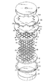
図1は、この発明の第1の実施形態に係る圧接型半導体装置の断面図である。図2は図1の圧接型半導体装置を外囲器から取り出して分解した状態の要部を示す分解図である。この第1実施形態では、複数の圧接型IGBTチップと、これらIGBTチップにそれぞれ通電方向を逆にして並列接続される複数のFRD(フリーホイールダイオード)チップとを圧接してマルチチップ圧接型半導体装置を構成している。
【0010】
図1及び図2において、10は例えばセラミック製の外囲器、11,11,…はIGBTチップ、12,12,…はFRDチップ、13,13,…は各チップ11,11,…,12,12,…の四辺を固定し、水平方向に対する位置ずれを防止するための枠状のチップフレームである。これらチップフレーム13,13,…は、シリコーン樹脂やポリエーテルイミド等からなり、各チップ11,11,…,12,12,…に接着剤等を用いて固着される。また、14,14,…は厚さが1〜2mmのモリブデン板等からなる熱緩衝板(エミッタ側熱緩衝板)で、この熱緩衝板14,14,…は、各チップ11,11,…,12,12,…のコーナー部に荷重が集中するのを防止するために、四隅が0.2〜1mmの曲率半径になっている。15は円板型熱緩衝板(コレクタ側熱緩衝板)、16は樹脂フレーム、17はリングフレームである。上記樹脂フレーム16の中央部には各チップ11,11,…,12,12,…に対応する位置に開口18,18,…が設けられ、格子状の枠が形成されており、外周部には爪19,19,…が設けられている。一方、リングフレーム17には上記円板型熱緩衝板15に対応する開口20が設けられ、且つ上記爪19,19,…に対応する位置に係合穴21,21,…が設けられており、上記爪19,19,…と係合穴21,21,…とを係止することにより、樹脂フレーム16とリングフレーム17とによって熱緩衝板14,14,…、チップフレーム13,13,…、IGBTチップ11,11,…、FRDチップ12,12,…、及び円板型熱緩衝板15を挟持する。
【0011】
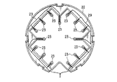
また、22は各チップ11,11,…,12,12,…に対応する位置に開口22aが形成された枠状の樹脂基板で、この樹脂基板22の裏面側には各IGBTチップ11,11,…のゲート電極に対応する位置にゲート圧接電極23,23,…、及び各IGBTチップ11,11,…を制御する制御信号を上記ゲート圧接電極23を介して各IGBTチップ11,11,…のゲート電極に供給するためのゲート配線が設けられている。上記ゲート圧接電極23,23,…は、図示しないバネによって各IGBTチップ11,11,…のゲート電極に圧接される。上記ゲート配線は樹脂基板22に固着されており、上記開口22aに対応する形状の開口24aを有する樹脂製の保護カバー24によって保護されている。すなわち、樹脂基板22の外周部には係合穴25,25,…が設けられ、保護カバー24の上記係合穴25,25,…に対応する位置には爪26,26,…が設けられ、これら係合穴24,24,…と爪26,26,…とを係止することにより、ゲート配線を保護するようになっている。
【0012】
なお、27はエミッタ圧接電極板、28はコレクタ圧接電極板で、上記エミッタ圧接電極板27の裏面側には、各IGBTチップ11,11,…、及びFRDチップ12,12,…に対応する位置に柱状の突起部が形成され、この突起部が上記樹脂基板22の開口22a、保護カバー24の開口24a、樹脂フレーム16の開口18,18,…、熱緩衝板14,14,…、及びチップフレーム13,13,…を介して各チップ11,11,…,12,12,…の主表面を圧接するようになっている。そして、このエミッタ圧接電極板27とコレクタ圧接電極板28とに高い圧力を印加して圧接した状態で用いられる。
【0013】
図3は、上記図1及び図2における各チップの配置を示す平面図である。図示するようにFRDチップ12,12,…は中央部に配置され、IGBTチップ11,11,…はFRDチップ12,12,…を囲むように周辺部に配置されている。そして、各FRDチップ12,12,…は、IGBTチップ11,11,…に逆並列に接続される。
【0014】
図4は、上記図1及び図2における樹脂基板22を裏面側から見た平面図である。この樹脂基板22には、各IGBTチップ11,11,…のゲート電極に対応する位置にゲート圧接電極23,23,…が設けられ、これらゲート圧接電極23,23,…にはゲート配線29,29,…が接続されている。ゲート配線29,29,…は1箇所でまとめられて外部に導出される。そして、このゲート配線29,29,…から制御信号が入力され、ゲート圧接電極23,23,…を介して各IGBTチップ11,11,…のゲート電極に供給されることによりオン/オフ制御される。
【0015】
図5(a)は図1及び図2における樹脂フレーム16の平面図、図5(b)は図5(a)に示した樹脂フレーム16の5B−5B線に沿った断面図、図5(c)は図5(b)に示した樹脂フレーム16の端部を拡大して示す断面図である。図5(a)に示すように、二点鎖線で示すIGBTチップ11,11,…及びFRDチップ12,12,…の境界位置に格子状の枠が形成され、これらチップ11,11,…,12,12,…を樹脂フレーム16で上方向から加圧して保持するようになっている。
【0016】
上記のような構成によれば、複数のIGBTチップ11,11,…を圧接しており、定格電流を増大させる際にはチップ11,11,…の数を増やせば良いので大容量化が容易にでき、且つ小さいサイズのIGBTチップ11,11,…を多数形成して良品のみを抽出して用いれば良いので、製造歩留まりの向上にも寄与できる。また、ゲート電極配線29,29,…を樹脂基板22に固着して配線するので振動等に強くなり、輸送時にゲート電極配線が短絡したり断線する恐れがほとんどなく、ゲート電極配線29,29,…の信頼性を向上できる。しかも、IGBTチップ11,11,…を周辺部に配置したので、ゲート圧接電極23,23,…を樹脂基板22に容易に設けることができ、且つゲート電極配線29,29,…の配線長を短くできるので配線が容易で且つ断線や短絡の可能性がより低くなり、この点からも信頼性を向上できる。ゲート電極配線29,29,…の配線長を短くできるので、インダクタンス成分の低減も図れる。更に、樹脂フレーム16とリングフレーム17とで、熱緩衝板14,14,…、チップフレーム13,13,…、IGBTチップ11,11,…、FRDチップ12,12,…、及び円板型熱緩衝板15を上下方向から挟むことにより、各チップ11,11,…,12,12,…の上下方向の位置出し及び固定を行うので、両圧接電極板27,28に圧力が印加されていない状態、例えば輸送する時の振動等によるチップの位置ずれを防止でき、誤圧接による不良を防止して信頼性を向上できる。
【0017】
なお、上記第1実施形態では、各チップ11,11,…,12,12,…上に熱緩衝板14,14,…を設けたが、各チップ11,11,…,12,12,…とこれら熱緩衝板14,14,…との間にそれぞれ、Cu等からなる軟金属箔を介在させれば電気的な接触を良好にできる。更に、エミッタ圧接電極板27と熱緩衝板14,14,…との間、及び各チップ11,11,…,12,12,…と円板型熱緩衝板15との間の少なくとも一方に銀シートを介在させれば、各チップ11,11,…,12,12,…と熱緩衝板14,14,…の厚さのばらつきによる圧接圧力のばらつきを吸収でき、圧接時に各チップ11,11,…,12,12,…に均一な圧力を印加できる。
【0018】
また、上記第1実施形態では、樹脂フレーム16とリングフレーム17を係止すると共に、樹脂基板22と保護カバー24を係止したが、更にリングフレーム17と保護カバー24、及び樹脂フレーム16と樹脂基板22の少なくとも一方を係止するようにしても良い。
【0019】
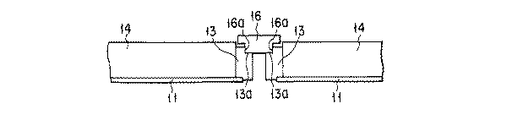
図6は、この発明の第2の実施形態に係る圧接型半導体装置について説明するためのもので、IGBTチップ11,11,…(FRDチップ12,12,…も同様)、チップフレーム13,13,…、熱緩衝板14,14,…及び樹脂フレーム16の接合部近傍を抽出して示している。すなわち、チップフレーム13の外周に切り欠き部13a,13a,…を設け、且つ樹脂フレーム16のチップフレーム13との接触部に対応する形状の突起部16a,16a,…を設け、チップフレーム13と樹脂フレーム16と係止することにより、各チップ11,11,…の上下方向の位置出し及び固定に加えて、チップ毎に水平方向の位置出しも行えるようにしたものである。
【0020】
このような構成によれば、上下方向と水平方向の位置出しとチップの固定ができるので、両圧接電極板27,28に圧力が印加されていない状態、例えば輸送時の振動等によりチップ11,11,…,12,12,…の位置ずれが生じることはなく、誤圧接による不良を確実に防止できる。
【0021】
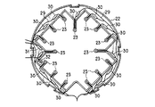
図7は、この発明の第3の実施形態に係る圧接型半導体装置について説明するためのもので、樹脂基板22上に抵抗30,30,…、サーミスタ31、及び電流検出素子32等を設けている。抵抗30,30,…は、IGBTチップが発振するのを防止するゲート抵抗であり、ゲート配線29,29,…とゲート圧接電極23,23,…との間に介在されている。サーミスタ31は、圧接型半導体装置の温度を監視して異常な高温になるのを防止するためのもので、外部の温度検出回路に接続される。電流検出素子32は、IGBTチップ11に流れる電流を監視して過電流が流れるのを防止するためのもので、外部の過電流検出回路に接続される。
【0022】
このような構成によれば、樹脂基板22に各種の素子を実装できるので、インテリジェント化が容易に実現できる。また、振動に対しても耐性が高い。
【0023】
なお、IGBTのゲート,エミッタ間にゲート過電圧防止用のために30V程度のツェナーダイオードを接続したり、ゲート,エミッタ間にコンデンサを挿入しても良い。これらツェナーダイオードやコンデンサは樹脂基板22に実装する。また、電流検出素子32だけでなく他の素子も含む過電流検出回路やIGBTチップ11,11,…を保護するための保護回路等を実装することもできる。
【0024】
図8は、この発明の第4の実施形態に係る圧接型半導体装置について説明するためのもので、上記第1ないし第3の実施形態では各IGBTチップ11,11,…がセンターゲートの場合の構成を例にとって説明したが、コーナーゲートのIGBTチップに適用する場合の樹脂基板22の構成例を示している。コーナーゲートのIGBTチップを用いると、センターゲートのIGBTチップに比してゲート配線29,29,…をより短縮することができ、配線が容易で且つ断線や短絡の可能性が低くなり、より信頼性を向上できる。しかも、ゲート配線29,29,…のインダクタンスも低減できる。
【0025】
なお、この発明は上述した第1ないし第4の実施形態に限定されるものではなく、要旨を逸脱しない範囲で種々変形して実施可能である。例えば上記各実施形態では圧接型半導体装置の一例として逆導通圧接型IGBTを例にとって説明したが、他の素子を用いた圧接型半導体装置にも同様に適用可能なのは勿論である。
【0026】
【発明の効果】
以上説明したように、この発明によれば、大容量化が容易にでき、且つ製造歩留まりの向上にも寄与できる圧接型半導体装置が得られる。
【0027】
また、複数の半導体チップを圧接した構造を採用した場合に輸送時の振動等による半導体チップの位置ずれによる誤圧接を防止できる圧接型半導体装置が得られる。
【図面の簡単な説明】
【図1】この発明の第1の実施形態に係る圧接型半導体装置の断面図。
【図2】図1の圧接型半導体装置を外囲器から取り出して分解した時の要部を抽出して示す分解図。
【図3】図1及び図2における各チップの配置を示す平面図。
【図4】図1及び図2における樹脂基板を裏面から見た時の平面図。
【図5】図1及び図2における樹脂フレームについて説明するためのもので、(a)図は平面図、(b)図は(a)図の5B−5B線に沿った断面図、(c)図は(b)図の端部を拡大して示す断面図。
【図6】この発明の第2の実施形態に係る圧接型半導体装置について説明するためのもので、IGBTチップ、チップフレーム、熱緩衝板及び樹脂フレームの接合部近傍を抽出して示す断面図。
【図7】この発明の第3の実施形態に係る圧接型半導体装置について説明するためのもので、樹脂基板の他の構成例を示す平面図。
【図8】この発明の第4の実施形態に係る圧接型半導体装置について説明するためのもので、コーナーゲートのIGBTチップに適用する場合の樹脂基板の更に他の構成例を示す平面図。
【符号の説明】
11,11,… …IGBTチップ(半導体チップ、第2の半導体チップ群)、12,12,… …FRDチップ(半導体チップ、第1の半導体チップ群)、13,13,… …チップフレーム、14,14,… …熱緩衝板、15…円板型熱緩衝板、16…樹脂フレーム(絶縁性フレーム)、17…リングフレーム、18,18,… …開口、19,19,… …爪、20…開口、21,21,……係合穴、22…樹脂基板(絶縁基板)、23,23,… …ゲート圧接電極(圧接電極)、24…保護カバー、25,25,… …係合穴、26,26,… …爪、27…エミッタ圧接電極板(第1の圧接電極板)、28…コレクタ圧接電極板(第2の圧接電極板)、29,29,… …ゲート配線(制御配線)、30,30,… …ゲート抵抗、31…サーミスタ、32…電流検出素子。[0001]
BACKGROUND OF THE INVENTION
The present invention relates to a pressure contact type semiconductor device that uses a plurality of semiconductor chips having control electrodes in a state of being pressure contacted together.
[0002]
[Prior art]
Conventionally, a structure in which a single semiconductor chip is sandwiched between pressure contact electrode plates is widely known as a pressure contact type semiconductor device. However, in this type of pressure contact type semiconductor device, in order to increase the rated current, it is necessary to increase the chip size. There is a problem that the manufacturing yield is lowered due to the increase.
[0003]
[Problems to be solved by the invention]
As described above, the conventional pressure contact type semiconductor device has a problem that it is difficult to increase the capacity. In addition, there is a high possibility that a defect that cannot be repaired will occur with an increase in capacity, resulting in a decrease in manufacturing yield.
[0004]
The present invention has been made in view of the circumstances as described above, and an object of the present invention is to provide a pressure contact type semiconductor device that can easily increase the capacity and contribute to an improvement in manufacturing yield. .
[0005]
Another object of the present invention is to provide a pressure contact type semiconductor device capable of preventing erroneous pressure contact due to positional deviation of a semiconductor chip due to vibration during transportation when a structure in which a plurality of semiconductor chips are pressure contacted is adopted.
[0006]
[Means for Solving the Problems]
The pressure contact type semiconductor device according to the present invention includes a plurality of semiconductor chips arranged on the same plane without using solder, and arranged on the main surface side of the plurality of semiconductor chips, and opened at positions corresponding to the semiconductor chips. An insulating frame, a disk-type heat buffer plate disposed on the back side of the semiconductor chip, a main surface of each semiconductor chip in the opening of the insulating frame, and the disk-type heat buffer plate The first and second pressure contact electrode plates that are in pressure contact with each other and the adjacent ones in contact with each other are disposed at positions corresponding to the openings of the insulating frame, and the main surfaces of the plurality of semiconductor chips and the first A frame-shaped chip frame interposed between the pressure contact electrode plates and fixing the four sides of each semiconductor chip, and each semiconductor chip is moved up and down by the insulating frame and the disk-type heat buffer plate. Sandwich from the direction And a, performs positioning and fixation of the vertical direction of the semiconductor chip, performs positioning and fixation of the horizontal direction of the semiconductor chip and the insulating frame and the chip frame.
[0007]
According to the above configuration, a plurality of semiconductor chips are press-contacted by the first and second press-contact electrode plates, and when the rated current is increased, the number of semiconductor chips may be increased, so that the capacity can be increased. It is easy to form a large number of small-sized semiconductor chips, and only good products can be extracted and used, which can contribute to an improvement in manufacturing yield.
[0008]
In addition, by sandwiching each semiconductor chip between the insulating frame and the disk-type heat buffer plate from above and below, each semiconductor chip is positioned and fixed in the vertical direction, and the insulating frame and the chip frame are Since each semiconductor chip is positioned and fixed in the horizontal direction, it is possible to prevent the chip from being displaced due to vibrations during transportation and the like, and it is possible to improve the reliability by preventing defects due to erroneous pressure contact.
[0009]
DETAILED DESCRIPTION OF THE INVENTION
An embodiment of the present invention will be described below with reference to the drawings.
FIG. 1 is a cross-sectional view of a pressure-contact type semiconductor device according to the first embodiment of the present invention. FIG. 2 is an exploded view showing a main part in a state where the pressure-contact type semiconductor device of FIG. 1 is taken out from the envelope and disassembled. In the first embodiment, a plurality of pressure-contact type IGBT chips and a plurality of FRD (free wheel diode) chips connected in parallel with the IGBT chips being reversed in the energization direction are press-contacted to form a multi-chip pressure-contact type semiconductor device. Is configured.
[0010]
1 and 2, 10 is, for example, a ceramic envelope, 11, 11, ... are IGBT chips, 12, 12, ... are FRD chips, 13, 13, ... are
[0011]
Further,
[0012]
In addition, 27 is an emitter press-contact electrode plate, 28 is a collector press-contact electrode plate, The position corresponding to each IGBT chip |
[0013]
FIG. 3 is a plan view showing the arrangement of the chips in FIGS. As shown in the figure, the FRD chips 12, 12,... Are arranged in the center portion, and the IGBT chips 11, 11,... Are arranged in the peripheral portion so as to surround the FRD chips 12, 12,. The FRD chips 12, 12,... Are connected to the IGBT chips 11, 11,.
[0014]
FIG. 4 is a plan view of the
[0015]
5A is a plan view of the
[0016]
According to the above configuration, a plurality of
[0017]
In the first embodiment, the
[0018]
In the first embodiment, the
[0019]
FIG. 6 is a view for explaining a pressure contact type semiconductor device according to the second embodiment of the present invention. The IGBT chips 11, 11,... (The same applies to the FRD chips 12, 12,...) And the chip frames 13, 13. ,..., The
[0020]
According to such a configuration, since the positioning in the vertical direction and the horizontal direction can be performed and the chip can be fixed, the
[0021]
FIG. 7 is for explaining a pressure contact type semiconductor device according to a third embodiment of the present invention.
[0022]
According to such a configuration, since various elements can be mounted on the
[0023]
Note that a Zener diode of about 30 V may be connected between the gate and emitter of the IGBT, or a capacitor may be inserted between the gate and emitter. These Zener diodes and capacitors are mounted on the
[0024]
FIG. 8 is for explaining a pressure contact type semiconductor device according to the fourth embodiment of the present invention. In the first to third embodiments, each
[0025]
The present invention is not limited to the first to fourth embodiments described above, and can be implemented with various modifications without departing from the scope of the invention. For example, in each of the above-described embodiments, the reverse conduction pressure-contact type IGBT is described as an example of the pressure-contact type semiconductor device. However, it is needless to say that the present invention can be similarly applied to a pressure-contact type semiconductor device using other elements.
[0026]
【The invention's effect】
As described above, according to the present invention, it is possible to obtain a pressure-contact type semiconductor device that can easily increase the capacity and contribute to an improvement in manufacturing yield.
[0027]
In addition, when a structure in which a plurality of semiconductor chips are press-contacted is adopted, a press-contact type semiconductor device that can prevent erroneous press-contact due to a positional deviation of the semiconductor chip due to vibration during transportation or the like can be obtained.
[Brief description of the drawings]
FIG. 1 is a cross-sectional view of a pressure-contact type semiconductor device according to a first embodiment of the present invention.
FIG. 2 is an exploded view showing a main part extracted when the pressure contact type semiconductor device of FIG. 1 is taken out from the envelope and disassembled.
3 is a plan view showing the arrangement of chips in FIGS. 1 and 2. FIG.
4 is a plan view when the resin substrate in FIGS. 1 and 2 is viewed from the back side. FIG.
FIGS. 5A and 5B are diagrams for explaining the resin frame in FIGS. 1 and 2, wherein FIG. 5A is a plan view, FIG. 5B is a cross-sectional view taken along line 5B-5B in FIG. The figure is a cross-sectional view showing an enlarged end of the figure.
FIG. 6 is a cross-sectional view showing an extracted portion in the vicinity of a junction of an IGBT chip, a chip frame, a thermal buffer plate, and a resin frame, for explaining a pressure-contact type semiconductor device according to a second embodiment of the present invention.
FIG. 7 is a plan view illustrating another configuration example of a resin substrate for explaining a press-contact type semiconductor device according to a third embodiment of the present invention.
FIG. 8 is a plan view illustrating still another configuration example of a resin substrate when applied to a corner gate IGBT chip, for explaining a pressure-contact type semiconductor device according to a fourth embodiment of the present invention.
[Explanation of symbols]
11, 11, ... IGBT chip (semiconductor chip, second semiconductor chip group) 12, 12, ... FRD chip (semiconductor chip, first semiconductor chip group) 13, 13, ... ... chip frame, 14 , 14,... Thermal buffer plate, 15 Disc type thermal buffer plate, 16 Resin frame (insulating frame), 17 Ring frame, 18, 18, ... Opening, 19, 19, ... Claw, 20 ... Opening, 21, 21, ... engagement hole, 22 ... resin substrate (insulating substrate), 23,23, ...... gate pressure contact electrode (pressure contact electrode), 24 ... protective cover, 25,25, ... engagement hole , 26, 26,... Claw, 27 ... emitter pressure contact electrode plate (first pressure contact electrode plate), 28 ... collector pressure contact electrode plate (second pressure contact electrode plate), 29, 29, ... gate wiring (control wiring) ), 30, 30,... Gate resistance, 31. Mista, 32 ... current detection element.
Claims (4)
前記複数の半導体チップの主表面側に配置され、前記各半導体チップに対応する位置に開口を有する絶縁性フレームと、
前記半導体チップの裏面側に配置される円板型熱緩衝板と、
前記絶縁性フレームの開口内の各半導体チップの主表面と前記円板型熱緩衝板とを一括して圧接する第1,第2の圧接電極板と、
隣接するもの同士が接した状態で前記絶縁性フレームの開口に対応する位置にそれぞれ配置され、前記複数の半導体チップの主表面と前記第1の圧接電極板との間に介在されて前記各半導体チップの四辺を固定する枠状のチップフレームと
を具備し、
前記絶縁性フレームと前記円板型熱緩衝板とで各半導体チップを上下方向から挟むことにより、各半導体チップの上下方向の位置出し及び固定を行い、
前記絶縁性フレームと前記チップフレームとで各半導体チップの水平方向の位置出し及び固定を行うことを特徴とする圧接型半導体装置。A plurality of semiconductor chips arranged without using solder on the same plane;
An insulating frame disposed on a main surface side of the plurality of semiconductor chips and having an opening at a position corresponding to each semiconductor chip;
A disk-type heat buffer plate disposed on the back side of the semiconductor chip;
First and second press-contact electrode plates that collectively press-contact the main surface of each semiconductor chip in the opening of the insulating frame and the disk-type heat buffer plate;
Each semiconductor is disposed at a position corresponding to the opening of the insulating frame in a state where adjacent ones are in contact with each other, and is interposed between a main surface of the plurality of semiconductor chips and the first pressure contact electrode plate. A frame-shaped chip frame for fixing the four sides of the chip,
Positioning and fixing each semiconductor chip in the vertical direction by sandwiching each semiconductor chip from the vertical direction with the insulating frame and the disk-type heat buffer plate,
A press-contact type semiconductor device, wherein the semiconductor frame is positioned and fixed in the horizontal direction by the insulating frame and the chip frame.
Priority Applications (1)
| Application Number | Priority Date | Filing Date | Title |
|---|---|---|---|
| JP2001331183A JP3766314B2 (en) | 2001-10-29 | 2001-10-29 | Pressure contact type semiconductor device |
Applications Claiming Priority (1)
| Application Number | Priority Date | Filing Date | Title |
|---|---|---|---|
| JP2001331183A JP3766314B2 (en) | 2001-10-29 | 2001-10-29 | Pressure contact type semiconductor device |
Related Parent Applications (1)
| Application Number | Title | Priority Date | Filing Date |
|---|---|---|---|
| JP13445195A Division JP3258200B2 (en) | 1985-05-31 | 1995-05-31 | Pressure contact type semiconductor device |
Publications (2)
| Publication Number | Publication Date |
|---|---|
| JP2002208542A JP2002208542A (en) | 2002-07-26 |
| JP3766314B2 true JP3766314B2 (en) | 2006-04-12 |
Family
ID=19146801
Family Applications (1)
| Application Number | Title | Priority Date | Filing Date |
|---|---|---|---|
| JP2001331183A Expired - Fee Related JP3766314B2 (en) | 2001-10-29 | 2001-10-29 | Pressure contact type semiconductor device |
Country Status (1)
| Country | Link |
|---|---|
| JP (1) | JP3766314B2 (en) |
-
2001
- 2001-10-29 JP JP2001331183A patent/JP3766314B2/en not_active Expired - Fee Related
Also Published As
| Publication number | Publication date |
|---|---|
| JP2002208542A (en) | 2002-07-26 |
Similar Documents
| Publication | Publication Date | Title |
|---|---|---|
| JP3258200B2 (en) | Pressure contact type semiconductor device | |
| US5949137A (en) | Stiffener ring and heat spreader for use with flip chip packaging assemblies | |
| US20070145540A1 (en) | Semiconductor device having semiconductor element, insulation substrate and metal electrode | |
| JP2570605B2 (en) | Semiconductor device | |
| EP2224484A1 (en) | Semiconductor module | |
| JPH0888240A (en) | Pressure-bonding type semiconductor device | |
| US20200035588A1 (en) | Semiconductor device | |
| US7956455B2 (en) | RF power transistor package | |
| JP3319569B2 (en) | Pressure contact type semiconductor device | |
| US10825751B2 (en) | Semiconductor device | |
| JP2591499B2 (en) | Semiconductor device | |
| CN116259594A (en) | Semiconductor device and method for manufacturing semiconductor device | |
| JP7163583B2 (en) | semiconductor equipment | |
| JP3766314B2 (en) | Pressure contact type semiconductor device | |
| JP2021158232A (en) | Semiconductor module | |
| JP3676091B2 (en) | Semiconductor device | |
| US11380608B2 (en) | Semiconductor module | |
| US10903138B2 (en) | Semiconductor device and method of manufacturing the same | |
| JPH0831490B2 (en) | Glass-sealed ceramic package | |
| JP3882648B2 (en) | Semiconductor device and manufacturing method thereof | |
| JPH0645515A (en) | Hybrid integrated circuit device | |
| JP4992302B2 (en) | Power semiconductor module | |
| JP6981033B2 (en) | Semiconductor devices and methods for manufacturing semiconductor devices | |
| JPH05243462A (en) | Semiconductor package | |
| JPS601838A (en) | Semiconductor device |
Legal Events
| Date | Code | Title | Description |
|---|---|---|---|
| A131 | Notification of reasons for refusal |
Effective date: 20050830 Free format text: JAPANESE INTERMEDIATE CODE: A131 |
|
| A521 | Written amendment |
Free format text: JAPANESE INTERMEDIATE CODE: A523 Effective date: 20051031 |
|
| A131 | Notification of reasons for refusal |
Free format text: JAPANESE INTERMEDIATE CODE: A131 Effective date: 20051122 |
|
| A521 | Written amendment |
Effective date: 20051227 Free format text: JAPANESE INTERMEDIATE CODE: A523 |
|
| TRDD | Decision of grant or rejection written | ||
| A01 | Written decision to grant a patent or to grant a registration (utility model) |
Free format text: JAPANESE INTERMEDIATE CODE: A01 Effective date: 20060124 |
|
| A61 | First payment of annual fees (during grant procedure) |
Effective date: 20060126 Free format text: JAPANESE INTERMEDIATE CODE: A61 |
|
| FPAY | Renewal fee payment (prs date is renewal date of database) |
Year of fee payment: 4 Free format text: PAYMENT UNTIL: 20100203 |
|
| FPAY | Renewal fee payment (prs date is renewal date of database) |
Year of fee payment: 4 Free format text: PAYMENT UNTIL: 20100203 |
|
| FPAY | Renewal fee payment (prs date is renewal date of database) |
Free format text: PAYMENT UNTIL: 20110203 Year of fee payment: 5 |
|
| FPAY | Renewal fee payment (prs date is renewal date of database) |
Free format text: PAYMENT UNTIL: 20120203 Year of fee payment: 6 |
|
| FPAY | Renewal fee payment (prs date is renewal date of database) |
Year of fee payment: 6 Free format text: PAYMENT UNTIL: 20120203 |
|
| FPAY | Renewal fee payment (prs date is renewal date of database) |
Free format text: PAYMENT UNTIL: 20130203 Year of fee payment: 7 |
|
| LAPS | Cancellation because of no payment of annual fees |