JP3759727B2 - Method for manufacturing flat light emitting display panel - Google Patents
Method for manufacturing flat light emitting display panel Download PDFInfo
- Publication number
- JP3759727B2 JP3759727B2 JP2002518490A JP2002518490A JP3759727B2 JP 3759727 B2 JP3759727 B2 JP 3759727B2 JP 2002518490 A JP2002518490 A JP 2002518490A JP 2002518490 A JP2002518490 A JP 2002518490A JP 3759727 B2 JP3759727 B2 JP 3759727B2
- Authority
- JP
- Japan
- Prior art keywords
- panel
- front panel
- frit
- flat
- manufacturing
- Prior art date
- Legal status (The legal status is an assumption and is not a legal conclusion. Google has not performed a legal analysis and makes no representation as to the accuracy of the status listed.)
- Expired - Fee Related
Links
Images


Classifications
-
- H—ELECTRICITY
- H01—ELECTRIC ELEMENTS
- H01J—ELECTRIC DISCHARGE TUBES OR DISCHARGE LAMPS
- H01J9/00—Apparatus or processes specially adapted for the manufacture, installation, removal, maintenance of electric discharge tubes, discharge lamps, or parts thereof; Recovery of material from discharge tubes or lamps
- H01J9/24—Manufacture or joining of vessels, leading-in conductors or bases
- H01J9/32—Sealing leading-in conductors
-
- H—ELECTRICITY
- H01—ELECTRIC ELEMENTS
- H01J—ELECTRIC DISCHARGE TUBES OR DISCHARGE LAMPS
- H01J9/00—Apparatus or processes specially adapted for the manufacture, installation, removal, maintenance of electric discharge tubes, discharge lamps, or parts thereof; Recovery of material from discharge tubes or lamps
- H01J9/24—Manufacture or joining of vessels, leading-in conductors or bases
- H01J9/26—Sealing together parts of vessels
- H01J9/261—Sealing together parts of vessels the vessel being for a flat panel display
Landscapes
- Engineering & Computer Science (AREA)
- Manufacturing & Machinery (AREA)
- Manufacture Of Electron Tubes, Discharge Lamp Vessels, Lead-In Wires, And The Like (AREA)
- Gas-Filled Discharge Tubes (AREA)
Description
技術分野
この発明は、電極を背面に引き出してパネル周囲をフリットガラスで封止する平面型発光表示パネルの製造方法に関するものである。
背景技術
近年の情報化社会の進展に伴い、大画面表示に対する需要が高まっている。一般に大画面を一枚の表示素子(以下、パネルという)で構成することは技術的にあるいはコスト的に困難である。このため、複数のパネルを配列して大画面を構成することが行われる。
この場合には、各パネルの端部に設けられた非表示領域が大きいと、隣接するパネル間の継ぎ目が目立つことになり、大画面全体における画面表示品位が低下してしまう。従って、各パネルの非表示領域が小さく、大画面表示を高品位で行う平面型発光表示パネルの開発が望まれている。
このような要求に応じて、先に本出願人が複数のパネルを配列した平面型発光表示パネルの構造を提案している。
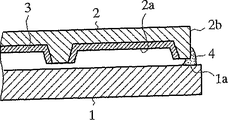
第1図はこの先行出願に係る平面型発光表示パネル(以下、表示パネルという)における側面封止構造を示す断面図である。図において1は透明な前面パネル、2は前面パネル1に対し平行に配設されかつ表示セルの放電空間となる複数の凹部2aを有する背面パネルである。この背面パネル2の凹部2aの底面および内壁面には絶縁ガラス層(図示せず)が形成され、この絶縁ガラス層上には蛍光体3が塗布されている。前面パネル1の内側には背面パネル2を貫通するピン電極(図示せず)が配設されている。また、前面パネル1には背面パネル2の凹部2aに対向する領域に一対のセル電極(図示せず)がそれぞれ配設されている。
このような構成からなる表示パネルでは、パネル端部における非表示領域を減じるために前面パネル1側の電極から、ピン電極(図示せず)によって背面に電極を取り出している。また、前面パネル1の外形寸法を背面パネル2の外形寸法よりも大きくして背面パネル2からはみ出した前面パネル1のはみ出し領域1aと背面パネル2の側面部2bとにフリット4を塗布し、焼成することによって前面パネル1と背面パネル2との周囲を封止するように構成されている。
次に、この表示パネルの製造方法について工程順に説明する。
(工程1)前面パネル1にITO(インジウム錫酸化物)またはネサ(酸化錫)等で放電ギャップを含む透明電極(図示せず)を形成する。
(工程2)工程1で形成した透明電極(図示せず)の一端にAg等の導電性材料を用いて電極端子(図示せず)をスクリーン印刷法で形成する。
(工程3)工程2で形成した電極端子(図示せず)部分を除いた前面パネル1全面に絶縁ガラス層(図示せず)をスクリーン印刷法で形成する。
(工程4)電極端子(図示せず)部分にピン電極(図示せず)を立設する。
(工程5)工程3で形成した絶縁ガラス層(図示せず)上にMgO膜を形成して前面パネル1に対する加工を終了する。
(工程6)背面パネル2にピン電極(図示せず)を貫通させるための貫通孔(図示せず)および表示セルの放電空間となる凹部2aをサンドブラスト法等で形成する。
(工程7)工程6で形成した凹部2aの底面および内壁面に蛍光体3(R,G,B)をスクリーン印刷法等で塗布して背面パネル2に対する加工を終了する。
(工程8)前面パネル1に立設したピン電極(図示せず)と背面パネル2の貫通孔(図示せず)とを位置合わせして、蛍光体3が前面パネル1に向くように背面パネル2を前面パネル1に重ね合わせる。
(工程9)ピン電極がない、前面パネル1の端部と背面パネル2の端部とをクリップばね(図示せず)で挟み両パネルを固定する。
(工程10)ピン電極(図示せず)にフリット4をディスペンサ(図示せず)で塗布する。
(工程11)工程10で塗布したフリット4を乾燥させた後、クリップばね(図示せず)を外し、チップ管部(図示せず)とパネル外周、即ち前面パネル1のはみ出し領域1aと背面パネル2の側面部2bにフリット4をディスペンサ(図示せず)で塗布する。
(工程12)チップ管部(図示せず)とピン電極(図示せず)を除いた部分にウェイト(図示せず)を置き、フリット4を焼成し、排気後に放電ガスを封入する。
(工程13)ピン電極(図示せず)に付着したMgOをサンドブラスト法等で除去して表示パネルを得る。
以上のような工程により製造された先行出願に係る表示パネルを複数配置し、点灯表示させると、隣接パネル間に表示の隙間が発生する場合がある。
この表示の隙間の発生原因を鋭意調査したところ、本発明者は、前面パネル1のはみ出し領域1aと背面パネル2の側面2bとに形成した封着フリットが表示セル内に滲むためであることを見出した。即ち、表示セル内に滲み出した封着フリットが背面パネル2に塗布されている蛍光体3またはこの蛍光体3に対応する前面パネル1の領域を被覆すると、その被覆部分は発光しないか、あるいは発光が遮られるため、パネル端部での非発光領域が増し、複数のパネルを並べて点灯させたときに隣接パネル間に表示の隙間が発生したように見えるという機作であると考えられる。
フリット滲みの発生は前面パネル1のはみ出し領域1aと背面パネル2の側面2bにフリット4を塗布するときに前面パネル1と背面パネル2との間に隙間が生じていることに原因があると考えられる。工程11でクリップばね(図示せず)を取り外し、フリット封着前に前面パネル1と背面パネル2との間を隙間ゲージ(図示せず)で測定したところ、0.15mm程度の隙間を確認した。この部分に大きな隙間があると、フリット4を塗布したときにフリット4の隙間への侵入量が多くなり、工程12でフリット4を焼成した際に軟化したフリット4がセル内へ滲み込む量が多くなる。
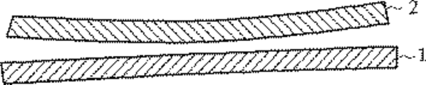
このような隙間は第2図に示すように前面パネル1と背面パネル2の反りに起因している。前面パネル1の表面には30μm厚程度の絶縁ガラス層(図示せず)が形成されており、また背面パネル2の表面には凹部2aが形成されているため、いずれも表面(対向面)が凸状に反る傾向にある。この状態で第3図に示すように両パネルの端部をクリップバネ5で挟むと(工程9)、両パネル1,2の中央部分が浮いた状態となるため、中央部分側に位置するピン電極をフリットで仮固定することになる(工程10)。なお、第2図および第3図では、背面パネル2の凹部2aおよびピン電極等の図示を省略している。次に、前面パネル1のはみ出し領域1aと背面パネル2の側面2bにフリット4を塗布するためにクリップバネ5を外すと、両パネルは元の形状に戻ろうとするため第2図に示すように両パネルの端部間に隙間が生じることになる。
さらに、フリット滲みの発生の他の要因としては、焼成時に前面パネル1と背面パネル2との微小間隙を、側面で軟化流動したフリット4が毛細管現象によって通過し、セル内に流れ込むことがある。このようなフリット滲みを減少させるためには、フリット4の軟化時の流動性を小さくすればよく、そのためにはフリット4の焼成条件を弱く(温度を低く、時間を短く)すればよいことが分かっている。
ところが、フリット4の焼成条件を弱くすると、フリット4のセル内への滲みを減少させることができるが、電圧を印加したときにピン電極で異常放電が発生する不具合を生じることがある。これはフリット4の焼成条件を弱くした場合に、フリット4の流動性が低くなるためにピン電極へ十分に流れこまず、ピン電極の被覆が不十分になり絶縁性が低下し、電圧を印加したときに異常放電が発生するものと考えられる。
逆に、ピン電極を完全に被覆するためにフリット4の焼成条件を強く(温度を高く、時間を長く)すると、パネルの端部のフリット4がセル内へ滲み出すという不具合を生じる。即ち、ピン電極の被覆とパネル端部のフリットの滲み出しは相反関係にあり、両者を両立させることは困難であった。
この発明は上記のような課題を解決するためになされたもので、ピン電極をフリットで完全に被覆すると共にパネル端部でのフリット滲みを低減できる平面型発光表示パネルの製造方法を提供することを目的とする。
発明の開示
この発明に係る平面型発光表示パネルの製造方法は、透明な前面パネルと、該前面パネルに対し平行に配設されかつ表示セルの放電空間となる複数の凹部が配列された背面パネルと、該背面パネルを貫通し前記前面パネルの内側に立設されたピン電極と、前記背面パネルの凹部に対向する前記前面パネルの領域にそれぞれ配設された一対のセル電極とを備え、前記ピン電極から前記セル電極への電圧供給が行われる平面型発光表示パネルの製造方法において、前記ピン電極に対応する位置に開口部を設けた平面板で前記背面パネルを前記前面パネルに押圧して両パネルを密着させた状態で、前記ピン電極にフリットを塗布し、乾燥させて前記両パネルを仮固定した後、前記平面板を外し、前記前面パネルの端部と前記背面パネルの側面部にフリットを塗布し、全体を焼成することを特徴とするものである。このことによって、平面板で両パネルを均一に密着させた状態で両パネルを仮固定することで、パネルの反りに起因する両パネル間の隙間の発生を防止し、フリットのパネル間の隙間への浸入を防止できる。また、フリットの焼成条件に強弱をつける必要がないので、ピン電極を十分に被覆できる条件でフリットを焼成することができる。
この発明に係る平面型発光表示パネルの製造方法は、平坦面を有するベース板に前面パネルおよび該前面パネルに重ねた背面パネルを載置し、平面板を前記ベース板にねじ締めする工程を含むことを特徴とするものである。このことによって、前面パネルおよび背面パネルを平面板とベース板との間に挟み、均一に密着させるので、フリットの塗布や焼成に際して両パネル間の隙間による滲みを確実に防止できる。
この発明に係る平面型発光表示パネルの製造方法は、平坦面を有するベース板に前面パネルおよび該前面パネルに重ねた背面パネルを載置し、平面板を複数の付勢手段を介して、前記ベース板にねじ締めする工程を含むことを特徴とするものである。このことによって、前面パネルおよび背面パネルを平面板とベース板との間に挟み、均一に密着させるので、フリットの塗布や焼成に際して両パネル間の隙間による滲みを確実に防止できる。
この発明に係る平面型発光表示パネルの製造方法は、前面パネルの端部と背面パネルの側面部に塗布するフリットを、ピン電極に塗布するフリットに比べて流動性の低いものとしたことを特徴とするものである。このことによって、両パネルの周囲から内部へ滲み込むフリット量を最小限に抑制することができる。
この発明に係る平面型発光表示パネルの製造方法は、透明な前面パネルと、該前面パネルに対し平行に配設されかつ表示セルの放電空間となる複数の凹部が配列された背面パネルと、該背面パネルを貫通し前記前面パネルの内側に立設されたピン電極と、前記背面パネルの凹部に対向する前記前面パネルの領域にそれぞれ配設された一対のセル電極とを備え、前記ピン電極から前記セル電極への電圧供給が行われる平面型発光表示パネルの製造方法において、前記ピン電極に対応する位置に開口部を設けた平面板で前記背面パネルを前記前面パネルに押圧して両パネルを密着させた状態で、前記前面パネルの端部と前記背面パネルの側面部にフリットを塗布し、乾燥させて前記両パネルを仮固定した後、前記平面板を外し、前記ピン電極にフリットを塗布し、全体を焼成することを特徴とするものである。このことによって、平面板で面パネルを均一に密着させた状態で両パネルを仮固定することで、パネルの反りに起因する両パネル間の隙間の発生を防止し、フリットのパネル間の隙間への浸入を防止できる。また、フリットの焼成条件に強弱をつける必要がないので、ピン電極を十分に被覆できる条件でフリットを焼成することができる。
この発明に係る平面型発光表示パネルの製造方法は、平坦面を有するベース板に前面パネルおよび該前面パネルに重ねた背面パネルを載置し、平面板を前記ベース板にねじ締めする工程を含むことを特徴とするものである。このことによって、前面パネルおよび背面パネルを平面板とベース板との間に挟み、均一に密着させるので、フリットの塗布や焼成に際して両パネル間の隙間による滲みを確実に防止できる。
この発明に係る平面型発光表示パネルの製造方法は、平坦面を有するベース板に前面パネルおよび該前面パネルに重ねた背面パネルを載置し、平面板を複数の付勢手段を介して、前記ベース板にねじ締めする工程を含むことを特徴とするものである。このことについて、前面パネルおよび背面パネルを平面板とベース板との間に挟み、均一に密着させるので、フリットの塗布や焼成に際して両パネル間の隙間による滲みを確実に防止できる。
この発明に係る平面型発光表示パネルの製造方法は、前面パネルの端部と背面パネルの側面部に塗布するフリットを、ピン電極に塗布するフリットに比べて流動性の低いものとしたことを特徴とするものである。このことによって、両パネルの周囲から内部へ滲み込むフリット量を最小限に抑制することができる。
【図面の簡単な説明】
第1図は先行出願に係る表示パネルにおける側面封止構造を示す断面図である。
第2図は前面パネルと背面パネルの反りの状態を示す断面図である。
第3図は第2図に示した前面パネルと背面パネルの反りを修正する方法を説明するための断面図である。
第4図はこの発明の実施の形態1による表示パネルの製造方法における工程前半を説明するための平面図である。
第5図は第4図のV−V線断面図である。
第6図はこの発明の実施の形態1による表示パネルの製造方法における工程後半を説明するための平面図である。
第7図は第6図のVII−VII線断面図である。
第8図はこの発明の実施の形態1による表示パネルの製造方法におけるピン電極へのフリット塗布工程を説明するための拡大断面図である。
第9図はこの発明の実施の形態2による表示パネルの製造方法における工程を説明するための平面図である。
第10図は第9図のX−X線断面図である。
第11図はこの発明の実施の形態3による表示パネルの製造方法における一工程を説明するための拡大断面図である。
発明を実施するための最良の形態
以下、この発明をより詳細に説明するために、この発明を実施するための最良の形態について、添付の図面に従ってこれを説明する。
実施の形態1.
第4図はこの発明の実施の形態1による表示パネルの製造方法における工程前半を説明するための平面図であり、第5図は第4図のV−V線断面図であり、第6図はこの発明の実施の形態1による表示パネルの製造方法における工程後半を説明するための平面図であり、第7図は第6図のVII−VII線断面図であり、第8図はこの発明の実施の形態1による表示パネルの製造方法におけるピン電極へのフリット塗布工程を説明するための拡大断面図である。なお、この実施の形態1の構成要素のうち第1図から第3図に示した先行出願に係る表示パネルの構成要素と共通するものについては同一符号を付し、その部分の説明を省略する。
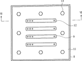
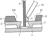
図において6は前面パネル1の電極部に取り付けられた電極ピンであり、7は背面パネル2に形成され前面パネル1の電極ピン6が貫通するための貫通スリット孔であり、8は前面パネル1および背面パネル2の相対位置を設定するための位置決め用ベースプレート(ベース板)であり、9はベースプレート8の四隅に形成されたねじ孔であり、10はベースプレート8の所定位置に立設された位置決めピンである。この位置決めピン10は段付きになっており、背面パネル2の側部が当接する上部10aの径は前面パネル1の側部が当接する下部10bの径よりも(前面パネル1の一辺の長さ−背面パネル2の一辺の長さ)/2だけ、大きく設定されている。
次にこの実施の形態1による表示パネルの製造方法を工程順に説明する。
まず、ベースプレート8上に前面パネル1および背面パネル2を重ねた状態で載置する。このとき、第4図および第5図に示すように前面パネル1の電極ピン6を背面パネル2の貫通スリット孔7に貫通させ、前面パネル1の側部を位置決めピン10の下部10bに矢印F1で示す力で押し当て、背面パネル2の側部を位置決めピン10の上部10aに矢印F2で示す力で押し当てることにより、前面パネル1と背面パネル2の中心合わせを行う。F1およびF2で示した押し当て力は手動押しでもよく、バネ等の付勢力でもよく、ネジ締め力でもよく、空気圧等でもよい。
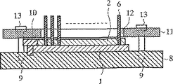
次に、第6図および第7図に示すように、背面パネル2を上方から押さえ板(平面板)11で押さえる。このとき、押さえ板11は電極ピン6に対応する位置に、背面パネル2の貫通スリット孔7と同様にスリット孔12を備えているため、このスリット孔12に電極ピン6を貫通させる。次に、ベースプレート8のねじ孔9にねじ13を螺合させ、締めることによりベースプレート8を押さえ板11で仮固定する。このとき、前面パネル1と背面パネル2はその全面にわたって押圧されることから、両パネル1,2は均一に密着する。このねじ13による固定は少なくともベースプレート8の四隅に形成されたねじ孔9に対して行われるものであるが、必要に応じて第6図に示すように押さえ板11の周囲に例えば8箇所に対して行われてもよい。
次に、押さえ板11とベースプレート8とを固定して両パネル1,2全面を押さえた状態で、第8図に示すように電極ピン6の基部であって背面パネル2の貫通スリット孔7内にフリット4をディスペンサ14で塗布する。フリット4は貫通スリット孔7を通して電極ピン6を被覆する。なお、押さえ板11は変形を防ぐためにある程度の厚さが必要とされるが、厚過ぎると電極ピン6にフリット4を塗布しにくくなるため、2mm〜3mm厚程度が好適であるが、これに限定されるものではない。また、フリット4の塗布を容易にするため、第8図に示すように、押さえ板11のスリット孔12の開口部にテーパ12aを設けている。
次に、フリット4を乾燥させた後、ベースプレート8および押さえ板11からなる治具から両パネル1,2を外す。この状態では電極ピン6は乾燥したフリット4で仮固定されている。仮固定された電極ピン6を支点としてパネルの反り力で変形しようとする傾向はあるが、パネル端部近傍に電極ピン6があるため変形は殆どなく、両パネル1,2はベースプレート8に沿って平面状態にある。
この状態で両パネル1,2の側面にフリット4をディスペンサ14で塗布する。このとき、前面パネル1と背面パネル2とが良好な平面状態で固定されているので、その端部の隙間は僅か(0.04mm以下)となるので、この隙間に入り込むフリット4の量も極めて少なくなる。
次に、チップ管をフリット4で固定した後、両パネル1,2にウェイト(図示せず)を載せた状態でフリット4を焼成し、両パネル1,2の周囲を封着する。このウェイト(図示せず)は電極ピン5およびチップ管部(図示せず)に孔を設けて両パネル1,2に対する押圧を避け、他の部分を均一に押圧する構造となっている。この押圧方法が均一でないと、焼成時にフリット4が軟化しているため、滲みが発生することになる。
以上のように、この実施の形態1によれば、押さえ板11で両パネル1,2を均一に密着させた状態で両パネル1,2を仮固定することで、パネルの反りに起因する両パネル1,2間の隙間の発生を防止し、フリット4のパネル間の隙間への浸入を防止できる。
この実施の形態1では、フリットの焼成条件に強弱をつける必要がないので、ピン電極6を十分に被覆できる条件でフリットを焼成することができる。
実施の形態2.
第9図はこの発明の実施の形態2による表示パネルの製造方法における工程を説明するための平面図であり、第10図は第9図のX−X線断面図である。なお、この実施の形態2の構成要素のうち実施の形態1の構成要素と共通する部分については同一符号を付し、その部分の説明を省略する。
この実施の形態2の特徴は、背面パネル2と押さえ板11との間に両者間の間隔を開けようとする方向に働く複数のコイルばね(付勢手段)15を適当な間隔で配置した点にある。このコイルばね15の付勢力により背面パネル2と押さえ板11との間隔が広がる方向に押されるから、押さえ板11からの背面パネル2への応力によって前面パネル1と背面パネル2とを均一に密着させることができる。
なお、この実施の形態2では、付勢手段としてのコイルばね15を押さえ板11の下面に凹部を設け、そのコイルばね15の一部を嵌め込むようにして配置しているが、付勢手段としては上記コイルばね15の形態に限るものではなく、例えば板ばね、エアーばねあるいはゴムブッシュのような弾力性を有するものであれば使用可能であり、要求される密着性の程度やコスト等を勘案して適宜使用することができる。
実施の形態3.
実施の形態1または2では、電極ピン6へのフリット塗布を行った後に、パネルの側部へのフリット塗布を行っていたが、この実施の形態3では、フリット塗布の順を逆にした点に特徴がある。即ち、この実施の形態3では、両パネル1,2全面を均一に押さえた状態でパネルの側部にフリットを塗布し、乾燥させて両パネル1,2を仮固定した後に、電極ピン6へのフリット塗布、焼成を行う。
この実施の形態3によれば、実施の形態1または2と同様に、両パネル1,2全面を均一に押さえた状態で前面パネル1と背面パネル2とを仮固定することができるので、パネルの反りに起因する両パネル1,2間の隙間の発生を防止し、フリット4のパネル間の隙間への浸入を防止できる。
また、この実施の形態3では、実施の形態1または2と同様に、両パネル1,2の全面を均一に押さえるのに押さえ板8を用いたが、第11図に示すようにウェイト16を用いることもできる。即ち、ウェイト16の下面にピン電極6との接触を避ける凹部16aを設けておき、前面パネル1上に重ねられた背面パネル2上に載置する。この状態で両パネル1,2の側部へのフリット塗布を行うことによって、ウェイト16が実施の形態1または2の場合における押さえ板11よりも重量を有するため、両パネル1,2間に生じる隙間を限りなく小さくすることができるので、フリット4の滲みを確実に防止することができる。また、このウェイト16を用いた実施の形態3では、押さえ板11を用いる必要がないため、部品の削減および工程の簡略化を図ることができる。
なお、両パネル1,2の全面を均一に押さえるウェイト16に代えて、例えばばね部材や圧力空気等も好適に使用することができる。
実施の形態4.
この実施の形態4の特徴は、パネルの側部へ塗布されるフリットを、電極ピン6へ塗布されるフリットよりも流動性の低いものを用いた点にある。このことによって、フリットによる被覆性とパネルの側部でのフリット滲みの低減をより確実に図ることができる。
フリットは例えばPbO・B2O3系ガラス粉末とセラミックス粉末等のフィラーとを混合したものであり、フィラーの材質や混合比、粒径等を変えることで軟化時の流動性を調整することができる。流動性を異ならせたフリットの組み合わせとしては、例えば日本電気硝子(株)製のLS−0118,LS−0206があり、その推奨封着温度条件はそれぞれ430℃、10分、450℃、15分となっている。即ち、この組み合わせでは、LS−0206がLS−0118に比べて同温度、同時間の焼成条件では流動性が低い。この特性を利用して、電極ピン6への塗布には相対的に流動性の高いLS−0118を用い、パネルの側部への塗布には相対的に流動性の低いLS−0206を用い、例えば445℃、15分の条件で焼成することによって電極ピン6に対しては流動性の高いフリットで完全に被覆すると共に、パネルの側部に対して流動性の低いフリットでその滲みを完全に抑制することができる。なお、上記LS−0118のフリットに代えて、同様の特性を有する例えば岩城硝子(株)製のDT−430を用いることもできる。
以上のように、この実施の形態4によれば、塗布する箇所に応じて流動性の異なるフリットを使い分けることによって、表示パネルに要求される表示品位を実現することができる。
産業上の利用可能性
以上のように、この発明に係る平面型発光表示パネルの製造方法は、パネル間の表示の隙間を発生しない表示パネルの製造に適しており、この表示パネルは、複数のパネルを配列した大画面表示に適している。TECHNICAL FIELD The present invention relates to a method for manufacturing a flat light emitting display panel in which electrodes are drawn out to the back and the periphery of the panel is sealed with frit glass.
BACKGROUND ART With the progress of the information society in recent years, there is an increasing demand for large screen displays. In general, it is technically or costly difficult to construct a large screen with a single display element (hereinafter referred to as a panel). For this reason, a large screen is configured by arranging a plurality of panels.
In this case, if the non-display area provided at the end of each panel is large, the seam between adjacent panels becomes conspicuous, and the screen display quality of the entire large screen is degraded. Accordingly, it is desired to develop a flat light emitting display panel that has a small non-display area of each panel and performs high-quality display on a large screen.
In response to such demands, the applicant has previously proposed a structure of a flat light emitting display panel in which a plurality of panels are arranged.
FIG. 1 is a sectional view showing a side surface sealing structure in a flat light emitting display panel (hereinafter referred to as a display panel) according to this prior application. In the figure,
In the display panel having such a configuration, in order to reduce the non-display area at the end of the panel, the electrode is taken out from the electrode on the
Next, the manufacturing method of this display panel will be described in the order of steps.
(Step 1) A transparent electrode (not shown) including a discharge gap is formed on the
(Step 2) An electrode terminal (not shown) is formed by screen printing on one end of the transparent electrode (not shown) formed in
(Step 3) An insulating glass layer (not shown) is formed on the entire surface of the
(Step 4) A pin electrode (not shown) is erected at an electrode terminal (not shown) portion.
(Step 5) An MgO film is formed on the insulating glass layer (not shown) formed in
(Step 6) A through hole (not shown) for penetrating a pin electrode (not shown) through the
(Step 7) The phosphor 3 (R, G, B) is applied to the bottom surface and the inner wall surface of the
(Step 8) A pin electrode (not shown) erected on the
(Step 9) An end portion of the
(Step 10) The frit 4 is applied to a pin electrode (not shown) with a dispenser (not shown).
(Step 11) After the frit 4 applied in
(Step 12) A weight (not shown) is placed on a portion excluding the tip tube portion (not shown) and the pin electrode (not shown), the frit 4 is fired, and discharge gas is sealed after exhausting.
(Step 13) MgO adhering to a pin electrode (not shown) is removed by a sandblast method or the like to obtain a display panel.
When a plurality of display panels according to the prior application manufactured by the above processes are arranged and lit, a display gap may be generated between adjacent panels.
As a result of diligent investigation on the cause of the gap in the display, the present inventor has found that the sealing frit formed in the protruding region 1a of the
The occurrence of frit bleeding is considered to be caused by a gap between the
Such a gap is caused by warpage of the
Further, as another cause of the occurrence of fritted bleeding, the frit 4 softened and fluidized on the side surface passes through the minute gap between the
However, if the firing conditions of the frit 4 are weakened, bleeding of the frit 4 into the cell can be reduced. However, when a voltage is applied, an abnormal discharge may occur at the pin electrode. This is because when the firing conditions of the frit 4 are weakened, the fluidity of the frit 4 is lowered, so that it does not flow sufficiently to the pin electrode, the pin electrode is not sufficiently covered, the insulation is lowered, and voltage is applied. It is considered that abnormal discharge occurs when
On the contrary, if the firing conditions of the frit 4 are increased (the temperature is increased and the time is increased) in order to completely cover the pin electrode, there is a problem that the frit 4 at the end of the panel oozes out into the cell. That is, the covering of the pin electrode and the exudation of the frit at the end of the panel are in a reciprocal relationship, making it difficult to achieve both.
The present invention has been made to solve the above-described problems, and provides a method for manufacturing a flat light-emitting display panel capable of completely covering a pin electrode with a frit and reducing frit bleeding at the end of the panel. With the goal.
DISCLOSURE OF THE INVENTION A method of manufacturing a flat light emitting display panel according to the present invention includes a transparent front panel and a rear panel arranged in parallel to the front panel and arranged with a plurality of recesses serving as display cell discharge spaces. A pin electrode penetrating through the back panel and erected on the inside of the front panel, and a pair of cell electrodes respectively disposed in a region of the front panel facing a recess of the back panel, In a method of manufacturing a flat light emitting display panel in which voltage is supplied from a pin electrode to the cell electrode, the back panel is pressed against the front panel with a flat plate provided with an opening at a position corresponding to the pin electrode. In a state where both panels are in close contact with each other, a frit is applied to the pin electrode, and after drying and temporarily fixing both the panels, the flat plate is removed, and the end of the front panel and the back panel are The frit was applied to face, it is characterized in firing the whole. This prevents the generation of a gap between the panels due to the warping of the panel by temporarily fixing both the panels in a state where the panels are evenly adhered to each other by a flat plate. Can be prevented. In addition, since it is not necessary to increase or decrease the frit firing conditions, the frit can be fired under conditions that can sufficiently cover the pin electrode.
A method for manufacturing a flat light emitting display panel according to the present invention includes a step of placing a front panel and a back panel overlaid on a base plate having a flat surface, and screwing the flat plate to the base plate. It is characterized by this. Accordingly, the front panel and the rear panel are sandwiched between the flat plate and the base plate and are in close contact with each other, so that bleeding due to the gap between the two panels can be reliably prevented during application and firing of the frit.
In the manufacturing method of the flat light emitting display panel according to the present invention, the front panel and the back panel overlaid on the front panel are placed on a base plate having a flat surface, and the flat plate is interposed through a plurality of biasing means. The method includes a step of screwing the base plate. Accordingly, the front panel and the rear panel are sandwiched between the flat plate and the base plate and are in close contact with each other, so that bleeding due to the gap between the two panels can be reliably prevented during application and firing of the frit.
The manufacturing method of the flat light emitting display panel according to the present invention is characterized in that the frit applied to the end portion of the front panel and the side surface portion of the back panel has lower fluidity than the frit applied to the pin electrode. It is what. This makes it possible to minimize the amount of frit that penetrates from the periphery of both panels.
A method of manufacturing a flat light emitting display panel according to the present invention includes a transparent front panel, a rear panel arranged in parallel to the front panel and having a plurality of recesses serving as discharge spaces of display cells, A pin electrode penetrating the back panel and erected on the inner side of the front panel; and a pair of cell electrodes respectively disposed in a region of the front panel facing the recess of the back panel; from the pin electrode In the method for manufacturing a flat light emitting display panel in which voltage is supplied to the cell electrode, the two panels are pressed by pressing the back panel against the front panel with a flat plate having an opening at a position corresponding to the pin electrode. In a state of being in close contact, frit is applied to the end portion of the front panel and the side surface portion of the back panel and dried to temporarily fix the both panels. Then, the flat plate is removed, and the pin electrode is attached to the pin electrode. Tsu DOO is applied, it is characterized in firing the whole. This prevents the generation of a gap between the two panels due to the warpage of the panel by temporarily fixing both panels in a state where the face panels are in close contact with the flat plate, and reduces the gap between the frit panels. Can be prevented. In addition, since it is not necessary to increase or decrease the frit firing conditions, the frit can be fired under conditions that can sufficiently cover the pin electrode.
A method for manufacturing a flat light emitting display panel according to the present invention includes a step of placing a front panel and a back panel overlaid on a base plate having a flat surface, and screwing the flat plate to the base plate. It is characterized by this. Accordingly, the front panel and the rear panel are sandwiched between the flat plate and the base plate and are in close contact with each other, so that bleeding due to the gap between the two panels can be reliably prevented during application and firing of the frit.
In the manufacturing method of the flat light emitting display panel according to the present invention, the front panel and the back panel overlaid on the front panel are placed on a base plate having a flat surface, and the flat plate is interposed through a plurality of biasing means. The method includes a step of screwing the base plate. In this regard, since the front panel and the rear panel are sandwiched between the flat plate and the base plate and are brought into close contact with each other, bleeding due to the gap between the two panels can be reliably prevented during application and firing of the frit.
The manufacturing method of the flat light emitting display panel according to the present invention is characterized in that the frit applied to the end portion of the front panel and the side surface portion of the back panel has lower fluidity than the frit applied to the pin electrode. It is what. This makes it possible to minimize the amount of frit that penetrates from the periphery of both panels.
[Brief description of the drawings]
FIG. 1 is a sectional view showing a side sealing structure in a display panel according to a prior application.
FIG. 2 is a cross-sectional view showing a warped state of the front panel and the back panel.
FIG. 3 is a cross-sectional view for explaining a method of correcting warpage of the front panel and the back panel shown in FIG.
FIG. 4 is a plan view for explaining the first half of the process in the method for manufacturing a display panel according to the first embodiment of the present invention.
FIG. 5 is a cross-sectional view taken along line VV in FIG.
FIG. 6 is a plan view for explaining the latter half of the process in the method for manufacturing a display panel according to
FIG. 7 is a sectional view taken along line VII-VII in FIG.
FIG. 8 is an enlarged cross-sectional view for explaining a frit coating step on the pin electrode in the display panel manufacturing method according to
FIG. 9 is a plan view for explaining a process in the display panel manufacturing method according to the second embodiment of the present invention.
FIG. 10 is a sectional view taken along line XX of FIG.
FIG. 11 is an enlarged cross-sectional view for explaining one step in the method for manufacturing a display panel according to
BEST MODE FOR CARRYING OUT THE INVENTION The best mode for carrying out the invention will now be described with reference to the accompanying drawings to explain the present invention in more detail.
FIG. 4 is a plan view for explaining the first half of the process in the method for manufacturing a display panel according to
In the figure, 6 is an electrode pin attached to the electrode portion of the
Next, the manufacturing method of the display panel according to the first embodiment will be described in the order of steps.
First, the
Next, as shown in FIGS. 6 and 7, the
Next, with the
Next, after the
In this state, the
Next, after fixing the tip tube with the
As described above, according to the first embodiment, both
In the first embodiment, since it is not necessary to increase or decrease the frit firing conditions, the frit can be fired under conditions that allow the
FIG. 9 is a plan view for explaining a process in the manufacturing method of the display panel according to the second embodiment of the present invention, and FIG. 10 is a sectional view taken along line XX of FIG. In addition, the same code | symbol is attached | subjected about the part which is common in the component of
The feature of the second embodiment is that a plurality of coil springs (biasing means) 15 that work in a direction to open a gap between the
In the second embodiment, the
In the first or second embodiment, after the frit application to the electrode pins 6 is performed, the frit application to the side of the panel is performed. However, in the third embodiment, the order of the frit application is reversed. There is a feature. That is, in the third embodiment, the frit is applied to the side portions of the panels while the entire surfaces of both
According to the third embodiment, similarly to the first or second embodiment, the
In the third embodiment, as in the first or second embodiment, the
In addition, it replaces with the
The feature of the fourth embodiment is that the frit applied to the side portion of the panel is lower in fluidity than the frit applied to the electrode pins 6. As a result, it is possible to more reliably reduce the frit coverage and frit bleeding at the side of the panel.
The frit is a mixture of, for example, PbO · B 2 O 3 glass powder and a filler such as ceramic powder, and the fluidity at the time of softening can be adjusted by changing the filler material, mixing ratio, particle size, etc. it can. For example, LS-0118 and LS-0206 manufactured by Nippon Electric Glass Co., Ltd. can be used as a combination of frits having different fluidity, and the recommended sealing temperature conditions are 430 ° C., 10 minutes, 450 ° C., and 15 minutes, respectively. It has become. That is, in this combination, LS-0206 is less fluid than LS-0118 under the same temperature and simultaneous firing conditions. Using this characteristic, LS-0118 having a relatively high fluidity is used for application to the electrode pins 6, and LS-0206 having a relatively low fluidity is used for application to the side of the panel. For example, by firing at 445 ° C. for 15 minutes, the electrode pins 6 are completely covered with a highly fluid frit and the bleeding is completely eliminated with a low fluid frit on the side of the panel. Can be suppressed. In place of the LS-0118 frit, for example, DT-430 manufactured by Iwaki Glass Co., Ltd. can be used.
As described above, according to the fourth embodiment, the display quality required for the display panel can be realized by properly using the frit having different fluidity depending on the application location.
Industrial Applicability As described above, the method for manufacturing a flat light emitting display panel according to the present invention is suitable for manufacturing a display panel that does not generate a display gap between the panels. Suitable for large screen display with panels arranged.
Claims (8)
前記ピン電極に対応する位置に開口部を設けた平面板で前記背面パネルを前記前面パネルに押圧して両パネルを密着させた状態で、前記ピン電極にフリットを塗布し、乾燥させて前記両パネルを仮固定した後、前記平面板を外し、前記前面パネルの端部と前記背面パネルの側面部にフリットを塗布し、全体を焼成することを特徴とする平面型発光表示パネルの製造方法。A transparent front panel, a rear panel arranged parallel to the front panel and arranged with a plurality of recesses serving as discharge spaces for display cells, and erected inside the front panel through the rear panel And a pair of cell electrodes respectively disposed in the region of the front panel facing the concave portion of the back panel, and a voltage is supplied from the pin electrode to the cell electrode. In the panel manufacturing method,
In a state where the rear panel is pressed against the front panel with a flat plate provided with an opening at a position corresponding to the pin electrode and the both panels are brought into close contact with each other, a frit is applied to the pin electrode, dried, and then the both After the panel is temporarily fixed, the flat plate is removed, a frit is applied to the end portion of the front panel and the side surface portion of the back panel, and the whole is fired.
前記ピン電極に対応する位置に開口部を設けた平面板で前記背面パネルを前記前面パネルに押圧して両パネルを密着させた状態で、前記前面パネルの端部と前記背面パネルの側面部にフリットを塗布し、乾燥させて前記両パネルを仮固定した後、前記平面板を外し、前記ピン電極にフリットを塗布し、全体を焼成することを特徴とする平面型発光表示パネルの製造方法。A transparent front panel, a rear panel arranged parallel to the front panel and arranged with a plurality of recesses serving as discharge spaces for display cells, and erected inside the front panel through the rear panel And a pair of cell electrodes respectively disposed in the region of the front panel facing the concave portion of the back panel, and a voltage is supplied from the pin electrode to the cell electrode. In the panel manufacturing method,
In a state where the back panel is pressed against the front panel with a flat plate provided with an opening at a position corresponding to the pin electrode and the both panels are brought into close contact with each other, the end of the front panel and the side surface of the back panel A method of manufacturing a flat light-emitting display panel, wherein frit is applied and dried to temporarily fix both panels, the flat plate is removed, the frit is applied to the pin electrode, and the whole is fired.
Applications Claiming Priority (1)
| Application Number | Priority Date | Filing Date | Title |
|---|---|---|---|
| PCT/JP2000/005289 WO2002013223A1 (en) | 2000-08-07 | 2000-08-07 | Method of producing planar type light-emitting display panels |
Publications (2)
| Publication Number | Publication Date |
|---|---|
| JPWO2002013223A1 JPWO2002013223A1 (en) | 2003-09-30 |
| JP3759727B2 true JP3759727B2 (en) | 2006-03-29 |
Family
ID=11736332
Family Applications (1)
| Application Number | Title | Priority Date | Filing Date |
|---|---|---|---|
| JP2002518490A Expired - Fee Related JP3759727B2 (en) | 2000-08-07 | 2000-08-07 | Method for manufacturing flat light emitting display panel |
Country Status (4)
| Country | Link |
|---|---|
| EP (1) | EP1308981A4 (en) |
| JP (1) | JP3759727B2 (en) |
| KR (1) | KR100445954B1 (en) |
| WO (1) | WO2002013223A1 (en) |
Families Citing this family (1)
| Publication number | Priority date | Publication date | Assignee | Title |
|---|---|---|---|---|
| KR101102494B1 (en) | 2007-06-08 | 2012-01-05 | 가부시키가이샤 아루박 | Method and apparatus for manufacturing sealing panel and method and apparatus for manufacturing plasma display panel |
Family Cites Families (4)
| Publication number | Priority date | Publication date | Assignee | Title |
|---|---|---|---|---|
| JPH07307131A (en) * | 1994-05-13 | 1995-11-21 | Canon Inc | Image forming apparatus manufacturing method |
| US6323596B1 (en) * | 1997-03-31 | 2001-11-27 | Mitsubishi Denki Kabushiki Kaisha | Planar display panel and panel manufacturing method |
| JP3442294B2 (en) * | 1998-09-29 | 2003-09-02 | 三菱電機株式会社 | Flat panel |
| JP2000133134A (en) * | 1998-10-22 | 2000-05-12 | Sony Corp | Frit sealing method for flat display device, jig for frit sealing and alignment device |
-
2000
- 2000-08-07 JP JP2002518490A patent/JP3759727B2/en not_active Expired - Fee Related
- 2000-08-07 WO PCT/JP2000/005289 patent/WO2002013223A1/en not_active Ceased
- 2000-08-07 KR KR10-2002-7004440A patent/KR100445954B1/en not_active Expired - Fee Related
- 2000-08-07 EP EP00950028A patent/EP1308981A4/en not_active Withdrawn
Also Published As
| Publication number | Publication date |
|---|---|
| EP1308981A4 (en) | 2006-02-15 |
| KR100445954B1 (en) | 2004-08-25 |
| EP1308981A1 (en) | 2003-05-07 |
| KR20020048950A (en) | 2002-06-24 |
| WO2002013223A1 (en) | 2002-02-14 |
Similar Documents
| Publication | Publication Date | Title |
|---|---|---|
| US6514111B2 (en) | Plasma display panel having a dielectric layer of a reduced thickness in a sealing portion | |
| JP3212837B2 (en) | Plasma display panel and method of manufacturing the same | |
| US5910705A (en) | Field emission display | |
| JPH0812348B2 (en) | Plasma addressed liquid crystal display device and manufacturing method thereof | |
| US5772486A (en) | Method for manufacturing a plasma-addressed display device | |
| JP3759727B2 (en) | Method for manufacturing flat light emitting display panel | |
| US3931436A (en) | Segmented gas discharge display panel device and method of manufacturing same | |
| US6686678B2 (en) | Flat panel display having mesh grid | |
| US6152796A (en) | Method for manufacturing an image forming apparatus | |
| JP2004071275A (en) | Display device and manufacturing method thereof | |
| US3944868A (en) | Segmented gas discharge display panel device | |
| JPWO2002013223A1 (en) | Method for manufacturing a flat-type light-emitting display panel | |
| US6746294B1 (en) | Method for fabricating a flat, light-emitting display panel | |
| JPS6375783A (en) | Electric field light emitting display panel | |
| JP3358385B2 (en) | Adhesive smoothing method | |
| KR920007086B1 (en) | Manufacturing method of plasma display panel | |
| JP4379092B2 (en) | Manufacturing method of display device | |
| US4119378A (en) | Segmented gas discharge display panel device and method of manufacturing same | |
| JPH01264137A (en) | Plasma display device | |
| JPS63226684A (en) | Electric field light emitting display panel | |
| JP3570239B2 (en) | Gas discharge panel | |
| US20070247054A1 (en) | Vacuum envelope, method of manufacturing the vacuum envelope, and electron emission display using the vacuum envelope | |
| JPH0722849Y2 (en) | Fluorescent display | |
| JP2984019B2 (en) | Phosphor dot array tube | |
| JPS5816433A (en) | Manufacture of gas discharge panel |
Legal Events
| Date | Code | Title | Description |
|---|---|---|---|
| TRDD | Decision of grant or rejection written | ||
| A01 | Written decision to grant a patent or to grant a registration (utility model) |
Free format text: JAPANESE INTERMEDIATE CODE: A01 Effective date: 20051206 |
|
| A61 | First payment of annual fees (during grant procedure) |
Free format text: JAPANESE INTERMEDIATE CODE: A61 Effective date: 20060104 |
|
| R150 | Certificate of patent or registration of utility model |
Free format text: JAPANESE INTERMEDIATE CODE: R150 |
|
| LAPS | Cancellation because of no payment of annual fees |