JP3748111B2 - Liquid crystal display - Google Patents
Liquid crystal display Download PDFInfo
- Publication number
- JP3748111B2 JP3748111B2 JP2005023661A JP2005023661A JP3748111B2 JP 3748111 B2 JP3748111 B2 JP 3748111B2 JP 2005023661 A JP2005023661 A JP 2005023661A JP 2005023661 A JP2005023661 A JP 2005023661A JP 3748111 B2 JP3748111 B2 JP 3748111B2
- Authority
- JP
- Japan
- Prior art keywords
- pixel electrode
- thin film
- pixel
- film transistor
- electrically connected
- Prior art date
- Legal status (The legal status is an assumption and is not a legal conclusion. Google has not performed a legal analysis and makes no representation as to the accuracy of the status listed.)
- Expired - Lifetime
Links
Images


Description
本発明は、アクティブマトリクス型の液晶表示装置及びその駆動方法に関するものである。 The present invention relates to an active matrix liquid crystal display device and a driving method thereof.
従来、表示装置としてCRTが最も一般的である。しかし、CRTは真空のガラスチューブを使用し、高電圧で電子を加速しているため、容積が大きい、重さが大きい、消費電力が大きい等の問題点がある。そのため、プラズマや、液晶を使ったフラットパネル型の表示装置が開発されている。特に近年、液晶表示装置のなかでも、アクティブマトリクス型の液晶表示装置が普及しつつある。 Conventionally, a CRT is the most common display device. However, since CRT uses a vacuum glass tube and accelerates electrons with a high voltage, there are problems such as large volume, large weight, and large power consumption. Therefore, flat panel display devices using plasma or liquid crystal have been developed. Particularly in recent years, among liquid crystal display devices, active matrix type liquid crystal display devices are becoming widespread.
図10は従来例のアクティブマトリクス型液晶表示装置の構成図であり、画素マトリクス1には、信号線2、走査線3により信号線駆動回路4、走査線駆動回路5が接続されている。
FIG. 10 is a block diagram of a conventional active matrix liquid crystal display device. A signal
図11は従来例の画素マトリクス1の構成図であり、ガラス基板上に、信号線11〜13、走査線14〜16がマトリクス状に配置され、その交差部分にそれぞれ薄膜トランジスタ17〜20が配置されている。薄膜トランジスタ17〜20において、ソース電極は信号線11〜13に接続され、ゲイト電極は走査線14〜16に接続されている。また、ドレイン電極は画素領域の液晶セル21〜24と、保持容量25〜28とに対応して配置された図示しない画素電極に接続されている。
FIG. 11 is a configuration diagram of a
図12は薄膜トランジスタ17〜20の電極に印加される電位の時間変化を示すグラス図であり、図12(a)は薄膜トランジスタのソース電極に印加される電位VS であり、図12(b)はゲイト電極に印加される電位VG であり、図12(c)はドレイン電極の電位VD である。
FIG. 12 is a glass diagram showing the time change of the potential applied to the electrodes of the
薄膜トランジスタ17〜20がNチャネルの場合、ゲイト電極がハイ(ゲイト電極の電位VG がプラス側)になると、薄膜トランジスタ17〜20はオンとなり、ソース電極の電位VS とドレイン電極の電位VD は等しくなるように動作する。この動作により、信号線11〜13の電位が保持容量25〜28に書き込まれる。次に薄膜トランジスタ17〜20のゲイト電極がロウ(ゲイト電極のマイナス側電位)になると、薄膜トランジスタ17〜20はオフとなり、ソース電極、ドレイン電極間はオープン状態になる。これによって、保持容量25〜28の電位は次に薄膜トランジスタ17〜20がオンになり、再び書き込みが発生するまでの間、保持される。また、対向電極と画素電極の間に挟まれた図11の液晶セル21〜24はその両電極の差電圧が印加され、その電圧に応じて光の偏光特性が変化する。そして、偏光板を介することにより、最終的に透過率が変化して、明暗が形成される。
When the
即ち、液晶表示装置は液晶物質が分子軸に対して平行方向と垂直方向とで誘電率が異なることを利用して、光の偏光や透過光量、さらには散乱量を制御することでON/OFFを制御して、明暗を表示する。液晶材料としてはTN液晶、STN液晶、強誘電性液晶等が一般的に使用されている。 That is, the liquid crystal display device uses the fact that the liquid crystal substance has different dielectric constants in the direction parallel to and perpendicular to the molecular axis, and controls the polarization of light, the amount of transmitted light, and the amount of scattering. To display light and dark. As the liquid crystal material, TN liquid crystal, STN liquid crystal, ferroelectric liquid crystal and the like are generally used.
また、画素を駆動する周辺駆動回路を作製する方法には、単結晶シリコンのトランジスタ集積回路で作製する方法と、ポリシリコンを利用した薄膜トランジスタで構成し、アクティブマトリクスと同じガラス基板上に一体的に作製する方法とがある。単結晶シリコンで作製された駆動回路はTABまたはCOGという形でアクティブマトリクスに接続されるのが普通である。他方、ポリシリコン薄膜トランジスタで作製する方法では、駆動回路はTABやCOGではなく、基板上の金属配線でアクティブマトリクスに接続される。 In addition, a peripheral driving circuit for driving a pixel includes a method of manufacturing a single crystal silicon transistor integrated circuit and a thin film transistor using polysilicon, and is integrally formed on the same glass substrate as the active matrix. There is a method of manufacturing. The drive circuit made of single crystal silicon is usually connected to the active matrix in the form of TAB or COG. On the other hand, in the method of manufacturing with a polysilicon thin film transistor, the drive circuit is connected to the active matrix not by TAB or COG but by metal wiring on the substrate.
従来のアクティブマトリクス型液晶表示装置では、液晶材料には低価格及び配向制御が容易な点から、主にTN液晶が使用されている。TN液晶は偏光板を介した状態で、図13に示すような透過率−印加電圧(V)特性を有する。図13に示すように、透過率−印加電圧(V)特性は曲線の勾配が比較的緩やかなため、TN液晶を用いた液晶表示装置は印加電圧により諧調表示が可能である。 In the conventional active matrix type liquid crystal display device, TN liquid crystal is mainly used as the liquid crystal material because of its low cost and easy alignment control. The TN liquid crystal has transmittance-applied voltage (V) characteristics as shown in FIG. As shown in FIG. 13, the transmittance-applied voltage (V) characteristic has a relatively gentle curve slope, so that a liquid crystal display device using TN liquid crystal can perform gradation display by the applied voltage.
しかしながら、TN液晶は印加する電圧に対する応答が遅いという問題点がある。一般にTN液晶を用いた液晶表示装置では、図14に示すように諧調が黒から白に変化した場合、またはその逆に白から黒に変化した場合には、10msecから数10msecの応答遅れが発生する。特に一つの表示画素に着目すると、黒から白に諧調が変化する際に、画素中心部の階調がまず変化して、これに遅れて、表示画素周辺部の諧調が変化していることが観察される。この応答の遅れは、画素領域の液晶の周辺部と中心部とでは、電界を加えた際における応答時間に違いが見られる現象に起因する。 However, the TN liquid crystal has a problem that the response to the applied voltage is slow. In general, in a liquid crystal display device using TN liquid crystal, when the tone changes from black to white as shown in FIG. 14 or vice versa, a response delay of 10 msec to several tens msec occurs. To do. In particular, when focusing on one display pixel, when the gradation changes from black to white, the gradation at the center of the pixel changes first, and after that, the gradation at the periphery of the display pixel changes. Observed. This delay in response is caused by a phenomenon in which there is a difference in response time when an electric field is applied between the peripheral portion and the central portion of the liquid crystal in the pixel region.
図15(a)、(b)に基づいて、上記の現象を説明する。画素電極に電圧を印加した状態での図15(a)は液晶セル内の液晶分子の模式図であり、図15(b)は液晶セルの画素電極間の電気力線の模式図である。図15(a)に示すように、液晶セルは一対のガラス基板31、32間に液晶分子33が挟まれており、ガラス基板31、32には一対の透明な画素電極34、35が対向して設けられている。更に、図示される構成要素以外に配向膜やスイッチング用の薄膜トランジスタが設けられているが、図15(a)ではその記載は省略してある。また、図15(a)に示す構成を一対の偏向板で挟むことによって、最も基本的な構成の液晶表示装置を得ることができる。 The above phenomenon will be described with reference to FIGS. 15 (a) and 15 (b). FIG. 15A in a state where a voltage is applied to the pixel electrode is a schematic diagram of liquid crystal molecules in the liquid crystal cell, and FIG. 15B is a schematic diagram of electric lines of force between the pixel electrodes of the liquid crystal cell. As shown in FIG. 15A, in the liquid crystal cell, liquid crystal molecules 33 are sandwiched between a pair of glass substrates 31 and 32, and a pair of transparent pixel electrodes 34 and 35 are opposed to the glass substrates 31 and 32. Is provided. In addition to the components shown in the figure, an alignment film and a switching thin film transistor are provided, but the description thereof is omitted in FIG. Further, by sandwiching the configuration shown in FIG. 15A between a pair of deflecting plates, a liquid crystal display device having the most basic configuration can be obtained.
図15(a)に示すように、一対の画素電極34、35により電界が液晶分子33に印加されると、図15(b)に示す電気力線36に沿って、液晶分子33の分子軸が一様な方向に揃う。この結果、液晶分子33中を透過する光の偏光状態が変化する。 As shown in FIG. 15A, when an electric field is applied to the liquid crystal molecules 33 by the pair of pixel electrodes 34 and 35, the molecular axes of the liquid crystal molecules 33 are aligned along the electric force lines 36 shown in FIG. Are aligned in a uniform direction. As a result, the polarization state of the light transmitted through the liquid crystal molecules 33 changes.
しかしながら、画素電極34、35の周縁部においては、境界面37を境として、右側、即ち中央よりの液晶分子33は向きを変えようと回転するのに対して、左側の液晶分子33はそのままの状態を保持しようとする。この結果、画素電極34、35間において、境界面37近傍の液晶分子33は応答速度が画素電極34、35の中央付近の変化速度に比べて遅い。 However, at the periphery of the pixel electrodes 34 and 35, the liquid crystal molecules 33 from the right side, that is, the center, rotate to change the direction from the boundary surface 37, while the left liquid crystal molecules 33 remain as they are. Try to keep state. As a result, the response speed of the liquid crystal molecules 33 in the vicinity of the boundary surface 37 between the pixel electrodes 34 and 35 is slower than the change speed in the vicinity of the center of the pixel electrodes 34 and 35.
従来のアクティブマトリクス型液晶表示装置は、静止画をCRTと同等以上の画質で表示することが可能であるが、前述したような液晶分子の応答遅れのために、動画像の画質はCRTよりも低い。実際には、この応答遅れは高速で色調が変化した際の表示の不自然さ、動画表示の動きの鈍さとして現れる。 The conventional active matrix type liquid crystal display device can display a still image with an image quality equivalent to or better than that of a CRT. However, due to the response delay of liquid crystal molecules as described above, the image quality of a moving image is higher than that of a CRT. Low. Actually, this response delay appears as an unnatural display when the color tone changes at high speed and a dull motion of the moving image display.
上述の問題点を解消するために、本明細書で開示する主要な発明は、
透明基板上に信号線、走査線をマトリクス状に交差させ、その交差部分に薄膜トランジスタと透明画素電極を配置し、前記透明基板と異なる透明基板と、前記透明基板の間に液晶材料を挟み、前記液晶材料に電圧を印加して、表示を行うアクティブマトリクス型の液晶表示装置において、
透明画素電極は走査線、信号線に囲まれた画素領域のほぼ中央に位置する第1の画素電極と第1の画素電極の少なくとも2方向を囲む形状を有する第2の画素電極から成り、第1、第2の画素電極はそれぞれ異なる第1、第2の薄膜トランジスタに接続され、前記第1、第2の薄膜トランジスタはそれぞれ異なる信号線、走査線に接続されている。
In order to solve the above problems, the main invention disclosed in this specification is as follows.
Crossing signal lines and scanning lines in a matrix on a transparent substrate, disposing a thin film transistor and a transparent pixel electrode at the intersecting portion, sandwiching a liquid crystal material between the transparent substrate different from the transparent substrate, and the transparent substrate, In an active matrix type liquid crystal display device that performs display by applying a voltage to a liquid crystal material,
The transparent pixel electrode includes a first pixel electrode located substantially in the center of the pixel region surrounded by the scanning line and the signal line, and a second pixel electrode having a shape surrounding at least two directions of the first pixel electrode. The first and second pixel electrodes are connected to different first and second thin film transistors, respectively, and the first and second thin film transistors are connected to different signal lines and scanning lines, respectively.
図1は上記構成を有する表示装置の具体的な構成図であり、表示単位となる1つの画素セルのみを図示している。信号線107、108と走査線105、106は格子状に配置され、この格子部分の中央には透明電極から成る中央画素電極101が配置されている。更に、中央画素の略3辺を囲んで「コ」の字型の透明電極から成る周辺画素電極102が配置されている。周辺画素電極102は中央画素電極101の周囲のおよそ3/4を囲んでいる。中央画素電極101は第1の画素電極に相当し、周辺画素電極102は第2の画素電極に相当する。中央画素電極101には第1の薄膜トランジスタ103が接続され、周辺画素電極102には第2の薄膜トランジスタ104が接続されている。薄膜トランジスタ103には走査線105、信号線107が接続され、薄膜トランジスタ104には走査線106、信号線108が接続されている。
FIG. 1 is a specific configuration diagram of a display device having the above configuration, and shows only one pixel cell serving as a display unit. The
動画像を表示する際には、薄膜トランジスタ104をONにして、周辺画素電極102のみに電圧を印加する。そして所定のタイミングだけ遅らせて薄膜トランジスタ103をONにして、中央画素電極101にも電圧を印加する。即ち、最初に画素領域の周辺部のおよそ3/4の液晶が応答して、しかる後に画素領域の中心領域を占める液晶が遅れて応答する。
When displaying a moving image, the thin film transistor 104 is turned on and a voltage is applied only to the
従来例では、画素電極に電荷が印加されても、画素電極の周縁部の液晶は電極外の液晶の影響を受けて、応答が緩慢であったが、本発明では、あらかじめ応答に時間のかかる画素の周辺部の液晶を先に応答させ、しかる後に画素の中心領域の液晶を応答させている。更に、中央画素電極101、周辺画素電極102の動作タイミングを適宜設定することで、画素領域全体の液晶が立ち上がるタイミングを揃えている。その結果、見かけ上、画素セル内の液晶がほとんど同時に高速に応答するようにして、動画を正確に表示することができる。
In the conventional example, even when a charge is applied to the pixel electrode, the liquid crystal at the peripheral edge of the pixel electrode is affected by the liquid crystal outside the electrode, and the response is slow. However, in the present invention, the response takes time in advance. The liquid crystal in the peripheral part of the pixel is made to respond first, and then the liquid crystal in the central region of the pixel is made to respond. Furthermore, by appropriately setting the operation timings of the central pixel electrode 101 and the
上記のように動作させるには、第1の薄膜トランジスタ103、第2の薄膜トランジスタ104をそれぞれ異なる信号線、走査線を介して、異なる駆動回路によって、異なるタイミングで駆動する必要がある。具体的なタイミングの例としては、例えば第1の薄膜トランジスタ103を駆動するための画像信号を第2の薄膜トランジスタ104を駆動する画像信号よりも1フレーム期間の少なくとも1以上の自然数倍の時間遅れを有する信号とすればよい。 In order to operate as described above, the first thin film transistor 103 and the second thin film transistor 104 need to be driven at different timings by different driving circuits through different signal lines and scanning lines, respectively. As an example of specific timing, for example, the image signal for driving the first thin film transistor 103 is delayed by a natural number multiple of at least one frame period from the image signal for driving the second thin film transistor 104. It may be a signal that has.
また、中央画素電極101と周辺画素電極102とを離して配置しているが、この場合は、その離れる距離が重要である。図15(b)に示すように、一対の画素電極により電圧を印加した際には、画素の境界面から電気力線がはみだしているため、画素電極に挟まれていない液晶分子も応答している。図3は印加電圧に応答した液晶分子の位置を電極から離間距離として測定した結果を示す。5Vの電圧印加に対して、離間距離は4μm程度である。これは、5Vの電圧印加に対しては、画素電極から4μm程度離れた位置に在る液晶分子の向きを変化させることができることを意味している。従って、印加電圧を5Vとする場合には、図1において、中央画素電極101と周辺画素電極102の離間距離は4μm以内とすればよい。
Further, although the central pixel electrode 101 and the
更に、本明細書で開示する他の発明は、
液晶に電界を加えるための1単位の領域を有し、
前記1単位の領域には複数の電極が配置されており、
前記複数の電極として、
前記1単位の領域の周辺に接する領域の1/2以上を占める電極と、
前記1単位の領域における中心部分を占める電極と、
を少なくとも有することを特徴とする。
Furthermore, other inventions disclosed in this specification are:
Having a unit area for applying an electric field to the liquid crystal;
A plurality of electrodes are arranged in the one unit region,
As the plurality of electrodes,
An electrode occupying 1/2 or more of the area in contact with the periphery of the one unit area;
An electrode occupying a central portion in the one unit region;
It is characterized by having at least.
図1は上記構成を有する表示装置の具体的な構成図であり、画素領域として画定される1単位の画素領域は中央画素電極101と周辺画素電極102から構成され、表示の最小単位となるものである。表示単位となる画素領域の中心部分に中心画素電極101が配置され、中心画素電極101の周囲に、周辺画素電極102が配置されている。
FIG. 1 is a specific configuration diagram of a display device having the above-described configuration. One unit of pixel area defined as a pixel area is composed of a central pixel electrode 101 and a
上記の構成を有する発明において、中央画素電極の少なくとも1/2以上の領域が周辺画素電極で占められる必要がある。言い換えれば、表示単位の周辺部の領域を1/2以上を周辺画素電極占める必要がある。これは、中央画素電極下の液晶において、電極外部の液晶と接する部分の割合がその周囲全体に対して50%以上となると、周辺画素電極を中央画素電極よりも早いタイミングで駆動しても、画素領域周辺の液晶の影響による液晶の応答の遅れが顕著になるからである。図1に示す構成においては、画素領域の周辺に接する領域のおよそ3/4が周辺画素電極102によって占められ、中央画素電極下の液晶が電極外部の液晶と接する部分の割合はおよそ25%となっている。
In the invention having the above configuration, it is necessary that at least a half or more of the central pixel electrode is occupied by the peripheral pixel electrode. In other words, it is necessary to occupy more than half of the peripheral region of the display unit in the peripheral pixel electrode. In the liquid crystal under the central pixel electrode, when the ratio of the portion in contact with the liquid crystal outside the electrode is 50% or more with respect to the entire periphery, even if the peripheral pixel electrode is driven at an earlier timing than the central pixel electrode, This is because the response delay of the liquid crystal due to the influence of the liquid crystal around the pixel region becomes significant. In the configuration shown in FIG. 1, about 3/4 of the area in contact with the periphery of the pixel area is occupied by the
他の発明の構成は、
液晶に電界を加えるための1単位の領域を有し、
前記領域には複数の電極が配置されており、
前記複数の電極として、
前記1単位の領域の周辺に接する領域の1/2以上を占める電極と、
前記領域における中心領域を占める電極と、
を少なくとも有することを特徴とする。
Other aspects of the invention are:
Having a unit area for applying an electric field to the liquid crystal;
A plurality of electrodes are arranged in the region,
As the plurality of electrodes,
An electrode occupying 1/2 or more of the area in contact with the periphery of the one unit area;
An electrode occupying a central region in the region;
It is characterized by having at least.
他の発明の構成は、
液晶に電界を加えるための1単位の領域を有し、
前記領域には複数の電極が配置されており、
前記複数の電極として、
前記領域における中心部を占める電極と、
該電極周囲の1/2以上を囲んで配置された電極と、
を少なくとも有することを特徴とする。
Other aspects of the invention are:
Having a unit area for applying an electric field to the liquid crystal;
A plurality of electrodes are arranged in the region,
As the plurality of electrodes,
An electrode occupying a central portion in the region;
An electrode disposed around at least half of the circumference of the electrode;
It is characterized by having at least.
他の発明の構成は、
液晶を用いた表示を行う1単位の領域を有し、
前記1単位の領域の周辺に接する領域の1/2以上の領域に電界を加える手段と、
該手段からの電界が液晶に加えられた後に前記1単位の領域の中心部に電界を加える手段と、
を少なくとも有することを特徴とする。
Other aspects of the invention are:
It has one unit area for display using liquid crystal,
Means for applying an electric field to a region that is at least half of the region in contact with the periphery of the unit region;
Means for applying an electric field to the central portion of the one unit region after the electric field from the means is applied to the liquid crystal;
It is characterized by having at least.
上記構成を有する発明を図1を用いて具体的に説明する。図1には、中央画素電極101と周辺画素電極102で構成された1単位の領域が示されている。図1に示す構成においては、この1単位の領域が画素電極となる。ここで、中心画素電極101が1単位の領域の中心部を占める電極であり、周辺画素電極102がこの1単位の領域の周辺に接する領域のおよそ3/4の領域に電界を加えるための電極である。
The invention having the above configuration will be specifically described with reference to FIG. FIG. 1 shows an area of one unit composed of the central pixel electrode 101 and the
図1に示す構成においては、周辺画素電極102から液晶に対して電界を印加した後に、所定のタイミングを遅らせて、中心画素電極101から液晶に対して電界を印加する。こうして、画素領域の周辺に接する領域から画素領域の中心領域へと順次所定のタイニングで電界を加える構成を実現することができる。このため、応答の遅い画素領域の周辺に接した領域を最初に応答させることができ、結果として画素全体を一様に高速度で応答させることができる。
In the configuration shown in FIG. 1, after an electric field is applied from the
他の発明の構成は、
液晶の一部の領域に電界を加える手段を少なくとも有する表示装置であって、 前記手段は、
前記一部の領域の周辺に接する領域の1/2以上の領域にまず電界を加え、
その後に他の領域に電界を加える機能を有することを特徴とする。
Other aspects of the invention are:
A display device having at least means for applying an electric field to a partial region of liquid crystal, wherein the means includes:
First, an electric field is applied to a region that is 1/2 or more of the region in contact with the periphery of the partial region,
Then, it has a function of applying an electric field to another region.
他の発明の構成は、
液晶の所定の領域に電界を加える手段を少なくとも有する表示装置であって、 前記手段は、
前記所定の領域の周辺に接する少なくとも一部の領域から前記所定の領域の中心部および/または中心周辺部へと順次電界を加える機能を有することを特徴とする。
Other aspects of the invention are:
A display device having at least means for applying an electric field to a predetermined region of the liquid crystal,
It has a function of sequentially applying an electric field from at least a part of the region in contact with the periphery of the predetermined region to the central portion and / or the central peripheral portion of the predetermined region.
他の発明の構成は、
液晶の所定の領域に電界を加える手段を少なくとも有する表示装置であって、 前記手段は、
前記所定の領域の周辺に接する少なくとも一部の領域に電界を加えた後前記所定の領域の中心部および/または中心周辺部に電界を加える機能を有することを特徴とする。
Other aspects of the invention are:
A display device having at least means for applying an electric field to a predetermined region of the liquid crystal,
It has a function of applying an electric field to the central portion of the predetermined region and / or the central peripheral portion after applying an electric field to at least a part of the region in contact with the periphery of the predetermined region.
上記構成の具体的な例としては、図1に示すように、画素領域である所定の領域の周辺に接する領域に電界を加えるための周辺画素電極102と、所定の領域の中心部に電界を加えるための中央画素電極101を有する構成を挙げることができる。このような構成を採用することにより、画素領域となる液晶の所定の領域の周辺部から中心部へと順次に液晶を応答させることができ、画素領域周辺の液晶の影響による応答の遅れを補正することができる。
As a specific example of the above configuration, as shown in FIG. 1, a
さらに本明細書で開示する発明では、周辺画素電極を中央画素電極とは異なる面内に形成したことを特徴とする。このような構成を採用すると、中央画素電極の周辺領域に電界がより印加されやすくなる構成とすることができる。 Further, the invention disclosed in this specification is characterized in that the peripheral pixel electrode is formed in a different plane from the central pixel electrode. By adopting such a configuration, an electric field can be more easily applied to the peripheral region of the central pixel electrode.
また、上述の問題点を解消するために、本明細書で開示する発明の他の主要な構成は、
透明基板上に信号線、走査線をマトリクス状に交差させ、その交差部分に薄膜トランジスタと透明画素電極を配置し、前記透明基板と異なる透明基板と前記透明基板の間に液晶材料をはさみ、前記液晶材料に電圧を印加し、表示を行うアクティブマトリクス型液晶表示装置において、透明画素電極は走査線、信号線に囲まれた画素領域のほぼ中央に位置する第1の画素電極と第1の画素電極を囲む形状を持った第2の画素電極からなり、第1、第2の画素電極は、それぞれ異なる第1、第2の薄膜トランジスタに接続され、前記第1、第2の薄膜トランジスタはそれぞれ異なる信号線、走査線に接続され、前記第1の画素電極と前記第2の画素電極とは、異なる平面上に形成されていることを特徴とする。
In order to solve the above-described problems, other main configurations of the invention disclosed in this specification are as follows:
A signal line and a scanning line are crossed in a matrix on a transparent substrate, a thin film transistor and a transparent pixel electrode are arranged at the crossing portion, a liquid crystal material is sandwiched between the transparent substrate different from the transparent substrate, and the liquid crystal In an active matrix liquid crystal display device in which a voltage is applied to a material to perform display, a transparent pixel electrode is a first pixel electrode and a first pixel electrode which are located at substantially the center of a pixel region surrounded by scanning lines and signal lines. The first and second pixel electrodes are connected to different first and second thin film transistors, respectively, and the first and second thin film transistors are different signal lines. The first pixel electrode and the second pixel electrode are connected to a scanning line, and are formed on different planes.
更に、本発明の他の構成は、
透明基板上にマトリクス状に配置された透明画素電極を有し、前記透明画素電極は、走査線、信号線に囲まれた画素領域のほぼ中央に位置する第1の画素電極と第1の画素電極を囲む形状を持った第2の画素電極からなり、第1、第2の画素電極はそれぞれ異なる第1、第2の薄膜トランジスタに接続され、前記第1、第2の薄膜トランジスタはそれぞれ異なる信号線、走査線に接続され、前記第1の画素電極と前記第2の画素電極とは異なる平面上に形成されているアクティブマトリクス型の液晶表示装置において、入力された画像信号をフレームメモリによって遅延させ、原信号と比較を行い、動き部分を検出し、動き部分が検出された場合に、前記第2の薄膜トランジスタを、第1の薄膜トランジスタを駆動するより1フレーム以上先の画像信号を用いて駆動することを特徴とする。
Furthermore, another configuration of the present invention is as follows:
A transparent pixel electrode arranged in a matrix on a transparent substrate, wherein the transparent pixel electrode is a first pixel electrode and a first pixel located substantially in the center of a pixel region surrounded by scanning lines and signal lines; The second pixel electrode has a shape surrounding the electrode, and the first and second pixel electrodes are connected to different first and second thin film transistors, respectively, and the first and second thin film transistors are different signal lines. In an active matrix liquid crystal display device connected to a scanning line and formed on a different plane from the first pixel electrode and the second pixel electrode, an input image signal is delayed by a frame memory Compare with the original signal, detect the moving part, and when the moving part is detected, move the second thin film transistor one frame or more ahead of driving the first thin film transistor. And drives using image signals.
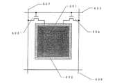
図6は上記発明の具体的な構成図であり、アクティブマトリクス方式の液晶表示装置における画素セルの構成図であり、図6(a)は画素の上面図を示し、図6(b)は図6(a)の線a−a’で切った断面図である。図6(a)に示すように、透光性を有する基板上に、従来の画素に対応する中央画素電極601が設けられ、更に、第2の画素電極として、周辺画素電極602が中央画素電極601の周辺に接し、その4辺を囲むように設けられている。中央画素電極601には画素薄膜トランジスタ603が接続され、周辺画素電極602には薄膜トランジスタ604が接続されている。
FIG. 6 is a specific configuration diagram of the above invention, and is a configuration diagram of a pixel cell in an active matrix liquid crystal display device. FIG. 6A shows a top view of the pixel, and FIG. It is sectional drawing cut | disconnected by line aa 'of 6 (a). As shown in FIG. 6A, a
更に、薄膜トランジスタ603、604にはそれぞれ走査線605、606、信号線607、608が独立に接続されている。更に、走査線605、606、信号線607、608にはそれぞれ図示しない駆動回路が独立に接続されている。このため、中央画素電極601と周辺画素電極602とを異なる駆動回路により、異なるタイミングで動作させることができる。
Further, scanning lines 605 and 606 and
また、図6(b)に示すように、周辺画素電極602は中央画素電極601の下層に配置されており、中央画素電極601が形成される層と周辺画素電極602が形成される層との間には、SiN、Al2 O3 等の絶縁膜層609が形成されている。
In addition, as shown in FIG. 6B, the
周辺画素電極602を中央画素電極601と異なる層に配置することにより、電気的に絶縁された層において、それぞれの電極に接続させる配線を設けることができる。例えば、中央画素電極601に接続された配線パターンを絶縁膜609上に形成することができるため、周辺画素電極602上を横断して配置することができる。従って、中央画素電極601の周囲を全て囲んで周辺画素電極602を配置することができる。
By disposing the
また、図6(b)に示すように、中央画素電極601と周辺画素電極602とは、中央画素電極601の周縁で重なるようにしている。このような構成を採用したため、中央画素電極601の周縁部分に対して、周辺画素電極602により、電圧を印加することができる。更に、中央画素電極601と周辺画素電極602とが部分的に重なっているために、プロセスでのアライメントのずれを補償することができる。このため、プロセスマージンを高めることができる。
Further, as shown in FIG. 6B, the
具体な動作としては、中央画素電極601に電圧が印加されるよりも先に周辺画素電極602間に電圧を印加する。すると周辺画素電極602に挟まれる液晶分子が長軸の方向が電気力線と平行になるように配向すると同時に、中央画素電極601の周縁の液晶分子もが分子の長軸の向きが初期配向状態から、電気力線に沿うようになるように変わる。便宜上これを第1の応答ということとする。
As a specific operation, a voltage is applied between the
次に、所定の時間遅れたタイミングで中央画素電極601にも電圧を印加する。これにより、中央画素電極601に挟まれる液晶分子が長軸の方向が電気力線と平行になるように配向する。便宜上、これを第2の応答という。
Next, a voltage is also applied to the
第2の応答において、周辺画素電極602からの電圧印加により、中央画素電極601の周縁の液晶分子は既に応答しているため、中央画素電極601間の液晶分子は位置に拘らず、応答の遅さが生じることがなく、中央画素電極の領域全体において均一に応答させることができる。
In the second response, since the liquid crystal molecules at the periphery of the
第1の応答に要する時間T1 と第2の応答に要する時間T2 との関係は、T1 >T2 となる。これは、第1の応答において、周辺画素電極602に挟まれる液晶分子は周辺の液晶分子の影響を受けて、その応答が遅くなるためである。ここで、ΔTをT1 −T2 =ΔTと定義する。本発明では、周辺画素電極602に電圧を印加してから中央画素電極601に電圧を印加するまでの時間差がΔTとなるようにする。これにより、中央画素電極の中央における液晶の応答と中央画素電極の縁近くの液晶の応答とが同時に応答したような状態が実現できる。このような動作状態は、動画の表示において、色調の変化や動画の動きを自然なものとするために非常に有用になる。
The relationship between the time T 1 required for the first response and the time T 2 required for the second response is T 1 > T 2 . This is because in the first response, the liquid crystal molecules sandwiched between the
なお、周囲画素電極602には、ブラックマトリクスを兼ねてクロムを用いることも可能である。これにより、画素周辺領域での液晶分子の配向乱れを遮蔽することができるという利点が生ずる。
Note that chromium can also be used for the surrounding
他の発明の構成は、
複数の画素電極が配置された画素領域を有する液晶表示装置であって、
前記画素領域には、
画素領域の中心領域を占める第1の画素電極と、
前記第1の画素電極の周囲全てを囲んで形成された第2の画素電極と、
を有することを特徴とする。
Other aspects of the invention are:
A liquid crystal display device having a pixel region in which a plurality of pixel electrodes are arranged,
In the pixel region,
A first pixel electrode occupying a central region of the pixel region;
A second pixel electrode formed surrounding the entire periphery of the first pixel electrode;
It is characterized by having.
上記構成において、画素領域というのは、例えば表示の一つの単位がマトリクス状に配置されている領域のことをいう。例えば、図6に示す構成の場合、周辺画素電極602と中央画素電極601で構成される領域が画素領域となる。
In the above configuration, the pixel region refers to a region where one unit of display is arranged in a matrix, for example. For example, in the case of the configuration shown in FIG. 6, a region formed by the
他の発明の構成は、
複数の画素電極が配置された画素領域を有する液晶表示装置であって、
前記画素領域には、
画素領域の中心領域を占める第1の画素電極と、
前記第1の画素電極の周囲の少なくとも一部を囲んで配置された第2の画素電極と、
を有し、
前記第1の画素電極と前記第2の画素電極とは異なる平面上に形成されていることを特徴とする。
Other aspects of the invention are:
A liquid crystal display device having a pixel region in which a plurality of pixel electrodes are arranged,
In the pixel region,
A first pixel electrode occupying a central region of the pixel region;
A second pixel electrode disposed surrounding at least a part of the periphery of the first pixel electrode;
Have
The first pixel electrode and the second pixel electrode are formed on different planes.
上記構成において、第1の画素電極と前記第2の画素電極とは異なる平面上に形成され、特に第1の画素電極の縁部分と第2の画素電極の一部とが重なることを特徴とする。 In the above structure, the first pixel electrode and the second pixel electrode are formed on different planes, and in particular, an edge portion of the first pixel electrode and a part of the second pixel electrode overlap with each other. To do.
具体的な構成としては、図6(b)に示す構成を採用できる。周辺画素電極602は中央画素電極601の下層に配置され、中央画素電極601が形成される層と周辺画素電極602が形成される層との間には、絶縁膜層609が形成されている。
As a specific configuration, the configuration shown in FIG. The
また、本明細書に開示する発明において、画素を駆動するための周辺駆動回路をポリシリコン薄膜トランジスタにより構成することが好ましい。周辺駆動回路をポリシリコン薄膜トランジスタで構成することにより以下の長所が生ずる。 In the invention disclosed in this specification, a peripheral driver circuit for driving a pixel is preferably formed using a polysilicon thin film transistor. Constructing the peripheral drive circuit with a polysilicon thin film transistor has the following advantages.
1、アクティブマトリクスの画素ピッチを小さくできる。
TABを用いてアクティブマトリクスを駆動する場合、TABのピッチは ガラス基板と張り合わせが可能な大きさに限定されるため、アクティブマ トリクスのピッチを小さくできない。
駆動回路を基板内に内蔵した場合アクティブマトリクスとの張り合わせが 存在しないため、マトリクスのピッチを小さくできる。
1. The pixel pitch of the active matrix can be reduced.
When an active matrix is driven using TAB, the pitch of TAB cannot be reduced because the pitch of TAB is limited to a size that can be bonded to a glass substrate.
When the drive circuit is built in the substrate, there is no bonding with the active matrix, so the matrix pitch can be reduced.
2、配線接続の信頼性が向上できる。
TABを用いる場合にアクティブマトリクスから外部に対して数千本の配 線が出力されるため、TAB−アクティブマトリクス基板の接続点におい て断線の確率が高いというのに対して、駆動回路を内蔵した場合アクティ ブマトリクス基板より外部にでる端子の数は百分の一程度となり信頼性の 向上が期待できる。
2. The reliability of wiring connection can be improved.
When TAB is used, thousands of wires are output from the active matrix to the outside, so there is a high probability of disconnection at the connection point of the TAB-active matrix substrate. In this case, the number of terminals coming out of the active matrix substrate is about one-hundredth, and improvement in reliability can be expected.
3、表示装置の大きさを小さくできる。
TABを用いる場合に画面の大きさが小さい表示装置、たとえばビュウフ ァインダの様なものではアクティブマトリクスよりも駆動回路のTABの 方が大きくなりビデオカメラ等の容積縮小の足かせとなっていた。駆動回 路内蔵の場合、回路の幅は5mm以下に抑えることが可能であるため、ビ ュウファインダ等の表示装置の小型化に貢献することが可能である。
3. The size of the display device can be reduced.
When a TAB is used, a display device having a small screen size, such as a viewfinder, has a larger TAB of the drive circuit than an active matrix, which has been a drag on the volume reduction of a video camera or the like. In the case of a built-in drive circuit, the circuit width can be suppressed to 5 mm or less, which can contribute to downsizing of a display device such as a viewfinder.
(作用)
本明細書で開示する発明は画素電極を中央画素電極と周囲画素電極に分離し、画面上で「動き」を要求される部分では予め周囲画素電極を駆動し、中央画素電極を駆動しようとしたときに、液晶材料が印加電圧に対して容易に応答させるようにしている。即ち、応答に時間のかかる画素の周辺に接する領域の液晶を先に応答させ、しかる後に画素の中心領域の液晶を応答させることによって、見かけ上、画素内の液晶がほとんど同時に高速に応答するようにしている。
(Function)
In the invention disclosed in this specification, the pixel electrode is separated into the central pixel electrode and the peripheral pixel electrode, and the peripheral pixel electrode is driven in advance in a portion where “movement” is required on the screen, and the central pixel electrode is driven. Sometimes the liquid crystal material is made to respond easily to the applied voltage. In other words, the liquid crystal in the area in contact with the periphery of the pixel, which takes time to respond, is made to respond first, and then the liquid crystal in the center area of the pixel is made to respond, so that the liquid crystal in the pixel responds almost simultaneously at high speed. I have to.
更に、本明細書で開示する発明では、画像信号をフレームメモリにより遅延させて、遅延前後の画像信号データを比較することにより、動き部分を検出して、動きが検出された場合には、上記のように周辺画素電極を先に駆動して、中央画素電極を1フレームの自然数倍ずらしたタイミングで駆動して、動画を正確に表示するようにする。 Further, in the invention disclosed in this specification, when a motion part is detected by delaying an image signal by a frame memory and comparing the image signal data before and after the delay, As described above, the peripheral pixel electrode is driven first, and the central pixel electrode is driven at a timing shifted by a natural number multiple of one frame, so that the moving image is accurately displayed.
本発明は画素を中央画素と周囲画素の2つの領域に分離して、画面に高速動作が要求される場合には、周辺画素をあらかじめ、中央画素に先行して動作させることにより、中央画素の動作速度を向上させる効果をもつ。従って、液晶表示装置の動作速度を向上すことが可能になり、より高画質な表示をユーザーに提供することが可能になる。 In the present invention, when a pixel is divided into two regions, a central pixel and a peripheral pixel, and a high-speed operation is required for the screen, the peripheral pixel is operated in advance before the central pixel. It has the effect of improving the operating speed. Therefore, the operation speed of the liquid crystal display device can be improved, and a higher quality display can be provided to the user.
図1は本明細書で開示する発明を利用して、アクティブマトリクス型の液晶表示装置の一つの画素セルの構成図である。従来では、1つの画素で構成されていた画素電極を本実施例では中央の画素電極と、その周囲を囲む画素電極とに分割することを特徴とする。 FIG. 1 is a configuration diagram of one pixel cell of an active matrix liquid crystal display device using the invention disclosed in this specification. Conventionally, a pixel electrode constituted by one pixel is divided into a central pixel electrode and a surrounding pixel electrode in this embodiment.
図1は上記構成を有する表示装置の具体的な構成図であり、表示単位となる1つの画素セルのみを図示している。信号線107、108と走査線105、106は格子状に配置され、この格子部分の中央には透明電極から成る中央画素電極101が配置され、中央画素の略3辺を囲んで「コ」の字型の透明電極から成る周辺画素電極102が配置されている。従って、周辺画素電極102は中央画素電極101の周囲のおよそ3/4を囲んでいる。中央画素電極101には第1の薄膜トランジスタ103が接続され、周辺画素電極102には第2の薄膜トランジスタ104が接続されている。薄膜トランジスタ103には走査線105、信号線107が接続され、薄膜トランジスタ104には走査線106、信号線108が接続されている。走査線105、106、信号線107、108にはそれぞれ図示しない駆動回路が独立に接続されている。
FIG. 1 is a specific configuration diagram of a display device having the above configuration, and shows only one pixel cell serving as a display unit. The signal lines 107 and 108 and the
図2は画素セルの断面構成図であり、透明基板110上に、中央画素電極101、周辺画素電極102が形成されている。他方の透明基板111上には、中央画素電極101に対向する中央画素電極112と、周辺画素電極102と対向する周辺画素電極113がそれぞれ形成されている。また、透明基板110、111間には、液晶114が封入されている。
FIG. 2 is a cross-sectional configuration diagram of a pixel cell, in which a central pixel electrode 101 and a
画素セルが表示すべき画面が静止画像の場合は、従来の方式の駆動方法を採用すればよく、中央の画素電極101が従来の画素電極と同じ役割を果して画面表示を行う。 When the screen to be displayed by the pixel cell is a still image, a conventional driving method may be employed, and the central pixel electrode 101 plays the same role as the conventional pixel electrode to perform screen display.
動画を表示する場合には、中央画素電極101の境界面(周囲と接する部分)の動作速度を改善するため、中央画素電極101、周辺画素電極102を異なるタイミングで駆動させ、動画を正確に表示するようする。最初に、周辺画素電極102、113のみにより電圧を印加する。図2(b)は、周辺画素電極102、113のみに電界を印加した状態での電気力線115の様子を示したものである。
When displaying a moving image, the central pixel electrode 101 and the
図2(b)に示すように、電気力線114は周辺画素領域の外側にも作用するため、周辺画素電極102、111に挟まれている液晶分子114をが応答させると共に中央画素電極101、112の周縁部の液晶分子114をも予め応答させて、その向きを変化させることができる。
As shown in FIG. 2B, the electric lines of force 114 also act outside the peripheral pixel region, so that the liquid crystal molecules 114 sandwiched between the
そして、中央画素電極101、112により中央画素電極101112に挟まれている液晶分子114に電界を印加する。この状態での液晶分子114を図2(a)に示めす。この状態では、中央画素電極101、112の周縁部の液晶分子が114予め応答しているので、電極101、102、112、113が配置されていない領域の液晶分子114の影響を受けずに、中央画素電極101、112の間の液晶分子114は円滑に応答することができる。
Then, an electric field is applied to the liquid crystal molecules 114 sandwiched between the central pixel electrodes 101112 by the
本実施例では、中央画素電極101、112と周辺画素電極102、113とを離して配置するようにしたが、その離す距離が重要になる。図2(a)に示すように一対の画素電極から電圧を印加した際に、画素の境界面から電気力線115がはみだす。その結果、周辺画素電極102、113の境界面の外側の液晶分子114も応答させることができる。
In this embodiment, the
図3は印加電圧に応答した液晶分子の位置を電極から離間距離として測定した結果を示す。5Vの電圧印加に対して、離間距離は4μm程度である。これは、5Vの電圧印加に対しては、画素電極から4μm程度離れた位置に在る液晶分子の向きを変化させることができることを意味している。従って、印加電圧を5Vとする場合には、図1において、中央画素電極101と周辺画素電極102の離間距離は4μm以内とすればよい。4μmの離間距離を形成するには、現在の液晶表示装置のフォトリソグラフィの解像度を考慮すると十分可能である。
FIG. 3 shows the result of measuring the position of the liquid crystal molecules in response to the applied voltage as the separation distance from the electrode. For a voltage application of 5V, the separation distance is about 4 μm. This means that when a voltage of 5 V is applied, the direction of liquid crystal molecules located at a position about 4 μm away from the pixel electrode can be changed. Therefore, when the applied voltage is 5 V, the distance between the central pixel electrode 101 and the
本実施例は、表示単位が2つの画素電極から成る画素マトリクスの駆動方法を示す。本実施例では、画素電極を実施例1と同じ構成とする。従って、中央画素電極、周辺画素電極を独立に動作させるために、それぞれに対してスイッチング素子となる薄膜トランジスタを独立に接続し、更に、これらの薄膜トランジスタ対して駆動回路を独立に接続する必要がある。 This embodiment shows a driving method of a pixel matrix whose display unit is composed of two pixel electrodes. In this embodiment, the pixel electrode has the same configuration as that of the first embodiment. Therefore, in order to operate the central pixel electrode and the peripheral pixel electrode independently, it is necessary to independently connect the thin film transistors serving as switching elements to each of them, and to connect the driving circuits to these thin film transistors.
一般に、周辺駆動回路は信号線駆動回路と走査線駆動回路とで構成される。これらの信号線駆動回路と走査線駆動回路とが一体的に動作して、各画素領域において1つの薄膜トランジスタを駆動することができる。本実施例では、中央画素領域と周辺画素領域において異なる動作を行う薄膜トランジスタが2つ配置されているので、信号線駆動回路と走査線駆動回路とはそれぞれ2組以上、最低でも2組必要となる。 In general, the peripheral driving circuit includes a signal line driving circuit and a scanning line driving circuit. These signal line driver circuit and scanning line driver circuit operate integrally to drive one thin film transistor in each pixel region. In this embodiment, two thin film transistors that perform different operations in the central pixel region and the peripheral pixel region are arranged. Therefore, two or more signal line driving circuits and two or more scanning line driving circuits are required. .
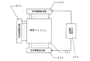
図4は本実施例の液晶表示装置の概略の構成図である。図4(a)に示すように、画素マトリクス401は、図1、2に示す中央画素電極、周辺画素電極から成る画素セルがマトリクス状に配置されている。中央画素電極に接続された薄膜トランジスタを制御するために、信号線駆動回路402、走査線駆動回路404がそれぞれ信号線、走査線により画素マトリクス401に接続されている。更に、周辺画素電極に接続された薄膜トランジスタを制御するために、信号線駆動回路403、走査線駆動回路605がそれぞれ信号線、走査線により画素マトリクス401に接続されている。信号線駆動回路402、403にはそれぞれ動き検出回路406の出力が接続されている。
FIG. 4 is a schematic configuration diagram of the liquid crystal display device of this embodiment. As shown in FIG. 4A, the
信号線駆動回路402、403、走査線駆動回路404、405は画素マトリクス401をの4辺を取り囲むように配置され、かつ、画素マトリクス401を隔てて、信号線駆動回路402と403が対峙し、走査線駆動回路404と405が対峙している。図4(b)は周辺駆動回路の配置の変形例であり、図4(a)と同じ符号は同じ部材を示している。図4(b)に示すように、画素マトリクス401の2辺を取り囲むように、信号線駆動回路402、403、走査線駆動回路404、405を配置して、かつ信号線駆動回路402と403及び走査線駆動回路404と405がそれぞれ同じ側に配置されている。ただし信号線駆動回路402、403、走査線駆動回路404、405はそれぞれ信号線、走査線を共有していない。
The signal
図5は信号線駆動回路402、403に表示信号を与えるためのシステムのブロック図であり、このシステムでは、外部から入力される画像信号はデジタル信号であり、システムから出力される信号もデジタル信号である。図5に示すように、フレームメモリ407、動き検出回路406にはそれぞれ外部から画像信号が入力される。フレームメモリ407の出力は動き検出回路406、信号線駆動回路403、フレームメモリ408にそれぞれ接続され、フレームメモリ408の出力は信号線駆動回路402に接続されている。
FIG. 5 is a block diagram of a system for supplying display signals to the signal
フレームメモリ407には外部から画像信号が入力されて、1フレーム分の画像データとして記憶される。フレームメモリ407は記憶している画像データをフレームメモリ408に出力する。フレームメモリ408はその画像データを記憶する。画像データをフレームメモリ408に出力すると、フレームメモリ407には新たな画像データが外部から入力されて、記憶されている画像データが更新される。即ち、フレームメモリ407は画像データをフレームメモリ408に出力する毎に、画像データが更新されるため、フレームメモリ407に記憶されている画像データはフレームメモリ408に記憶されている画像データよりも1フレーム先のデータとなる。
An image signal is input from the outside to the
動き検知回路406には、外部からの画像信号と、フレームメモリ407に記憶された画像データがそれぞれ入力される。動き検出回路406において、外部からの画像信号に「動き」の成分が在るか否かが判断される。フレームメモリ407から入力された画像データは外部からの画像信号よりも1フレーム後のデータとなるため、フレームメモリ407から入力された画像データを基準にして、外部から入力された画像信号から「動き」の成分を検出する。そのため入力された2つの画像データが減算されて、差分信号が作成され、この差分信号からノイズ成分を除去た後に、「動き」を現すものであるか、否かを判断する。
The
差分信号が「動き」を示すものでない場合には、動き検出信号406から駆動信号が信号線駆動回路402に出力されて、信号線駆動回路402は駆動信号が入力されると、信号線を介して薄膜トランジスタを駆動して、従来の画素電極と同様に、中央画素電極に画像データを書き込む。
When the difference signal does not indicate “motion”, a drive signal is output from the
差分信号が「動き」を示すものである場合には、動き検出信号406から駆動信号が信号線駆動回路403に出力される。信号線駆動回路403は駆動信号が入力されると、信号線を介して薄膜トランジスタを駆動して、周辺画素電極にフレームメモリ407に記憶されている画像データを書き込む。これと同時に、フレームメモリ407に記憶されている画像データはフレームメモリ408出力されて、遅延された後に、信号線駆動回路402により薄膜トランジスタを駆動して、中央画素に書き込まれて、中央画素と周辺画素には同一フレームの画像データが表示される。
When the difference signal indicates “motion”, a drive signal is output from the
このように、2つのフレームメモリ407、408に画像データを蓄積することにより、中央画素に書き込む画像データを遅延させて、かつ周辺画素に画像データを書き込むタイミングを中央画素よりも1フレーム先にすることができるため、実質的には、中央部と周辺部との応答の差が生じなくなり、動画像を正確に表示することが可能になる。
As described above, by storing image data in the two
図6の例ではデジタル信号処理を想定しているが、画像信号がアナログの場合には、フレームメモリ407、408に画像信号を入力する際には、ADコンバータによりデジタル信号に変換するようにして、信号線駆動回路402、403からの出力信号はDAコンバータにより、アナログ信号に変換して、画素マトリクスに出力するようにすればよい。
In the example of FIG. 6, digital signal processing is assumed. However, when the image signal is analog, when the image signal is input to the
本実施例は実施例1の変形例であり、中央画素電極と周辺画素電極とが重なるように配置することを特徴とする。画素セルは透光性を有する一対のガラス基板間にネマチック性を有する液晶材料を挟持した構成を有し、図6(a)は1つの画素領域の上面図であり、図6(b)は図6(a)の線a−a‘
で切った断面図である。また、図7は画素セルの断面構成図である。
The present embodiment is a modification of the first embodiment, and is characterized in that the central pixel electrode and the peripheral pixel electrode are arranged so as to overlap each other. The pixel cell has a structure in which a liquid crystal material having a nematic property is sandwiched between a pair of light-transmitting glass substrates. FIG. 6A is a top view of one pixel region, and FIG. Line aa ′ in FIG.
FIG. FIG. 7 is a cross-sectional configuration diagram of a pixel cell.
図6(a)に示すように、従来の画素に対応する中央画素電極601が設けられている。中央画素電極601の周辺に接して、その周辺を囲むように周辺画素電極602が設けられている。中央画素電極601には画素薄膜トランジスタ603が接続され、周辺画素電極602には画素薄膜トランジスタ604が接続されている。これらの薄膜トランジスタ603、604のゲイト電極、にはそれぞれ走査線605、606が接続され、ソース電極には信号線607、608が独立に接続されている。また、これらの走査線605、606、信号線607、608にはそれぞれ図示しない駆動回路が独立に接続されている。
As shown in FIG. 6A, a
また、図6(b)に示すように、周辺画素電極602は中央画素電極601の下層に配置されており、中央画素電極601が形成される層と周辺画素電極162が形成される層との間には、絶縁膜層609が形成されている。
Further, as shown in FIG. 6B, the
以下に液晶表示装置のアクティブマトリクスパネルの作製方法を説明する。第1の透明基板610として、コーニング社製の#7059ガラス基板(厚さ1.1mm)または#1713ガラス基板(厚さ1.1mm)を用いる。この透明基板610上に画素電極を駆動するための薄膜トランジスタ、周辺画素電極、及び中央画素電極をそれぞれ形成する。画素は必要とする数をマトリクス状に形成する。
A method for manufacturing an active matrix panel of a liquid crystal display device will be described below. As the first
通常のスパッタ法により、透明基板610上に、クロムを厚さ1000Åに成膜して、パターニングを施すことにより周辺画素電極602を形成する。この周辺画素電極602はブラックマトリクスとしても機能する。周辺画素電極602の形成と同時、その前に或いは後に、周辺画素電極602と薄膜トランジスタ604とを接続するための図示しない配線パターンを形成する。
The
周辺画素電極602上に、スパッタ法により酸化アルミニウム膜を成膜してパターニングして、絶縁膜609を形成する。なお、絶縁膜609を窒化珪素で形成してもよい。更に、絶縁膜609上に、厚さ1000ÅのITO膜をスパッタ法により成膜する。ITO膜をパターニングして、中心画素電極601を形成する。中心画素電極601の形成と同時、その前或いは後に、中央画素電極601と薄膜トランジスタ603とを接続するための配線パターンを形成する。
An insulating
ここで重要なことは、中央画素電極601と薄膜トランジスタ603を結ぶ配線は絶縁膜609上に形成され、周辺画素電極602と薄膜トランジスタ604とを結ぶ配線は絶縁膜609下に形成されることである。このような構成を採用することで、中央画素電極601と周辺画素電極602とを一部重ねて配置することや、中央画素電極601の周囲を全て囲んで周辺画素電極602を配置することができる。なお、第1の透明基板610上には、ここでは詳述しないが、周辺駆動回路領域等が薄膜トランジスタによって形成される。
What is important here is that a wiring connecting the
更に、第2の透明基板602として、コーニング社製#7059(厚さ1.1mm)または#1737(厚さ1.1mm)ガラス基板を用いる。その基板上に、第1の透明基板610に形成された、中央画素電極601、周辺画素電極602の対向電極をそれぞれ形成する。
Further, as the second
透明基板611上に、厚さ1000Åのクロムをスパッタ法により成膜する。そしてパターニングして、周辺画素電極602に対向する周辺画素電極612を形成する。この周辺画素電極612はブラックマトリクスとしても機能する。次に、周辺画素電極612上に、スパッタ法により酸化アルミニウム膜を成膜し、パターニングして、絶縁膜613を形成する。更に、絶縁膜613上に、厚さ1000ÅのITO膜をスパッタ法により成膜する。ITO膜をパターニングして、中心画素電極601との対向電極として中心画素電極614を形成する。この中心画素電極614は、パターニングせずに、全面にベタに形成されるものでよい。以上のプロセスにより、液晶表示装置を構成する一対の透光性基板が完成する。
A 1000-mm-thick chromium film is formed on the transparent substrate 611 by a sputtering method. Then, patterning is performed to form a peripheral pixel electrode 612 that faces the
次に、透明基板610、611の液晶に接する面に、液晶材料を配向制御するための図示しない配向膜を形成する。配向膜として、ポリイミド系樹脂を成膜して、ラビング処理を施す。本実施例ではTN型とするため、ラビングの方向は、透明基板610と611とで直交するようにする。
Next, an alignment film (not shown) for controlling the alignment of the liquid crystal material is formed on the surfaces of the
そして、所定の間隔を開けて透明基板610と611とをエポキシ系接着剤により張り合わせる。この際に、直径5.0μmの球形スペーサをにより透明基板610と611との間隔を制御する。そして、液晶材料を第1及び第2の基板610、611間に注入する。注入法としては、例えば真空注入法を用いればよい。
Then, the
静止画像を表示する際には、中央画素電極601、614を従来例と同様に駆動すればよい。中央画素電極601、614が従来の画素電極と同じ役割をして画面表示をおこなう。
When displaying a still image, the
動画を表示する際には、2種類の画素電極を異なるタイミングで動作させ、表示速度の向上を図る。そのため、周辺画素電極により電圧を印加して、所定のタイミング遅れて中央画素電極から電圧を印加するようにする。 When displaying a moving image, two types of pixel electrodes are operated at different timings to improve display speed. Therefore, a voltage is applied from the peripheral pixel electrode, and a voltage is applied from the central pixel electrode with a predetermined timing delay.
図7は、一対の透明基板610と611との間において、周辺画素電極602、612間のみに電圧を印加した状態を示し、図7(a)は電気力線615の様子を示したものであり、図7(b)は液晶分子616の状態を示したものである。
FIG. 7 shows a state in which a voltage is applied only between the
中央画素電極601、614に電圧が印加されるよりも先に周辺画素電極602、612間に電圧を印加する。このため、中央画素領域の周縁領域の液晶分子616が分子長軸の向きを電気力線615の向きに従うように初期配向状態から変化する。次に、少し遅れたタイミングで中央画素電極601、614にも電圧を印加する。中央画素電極601、614間に電圧が印加された状態では、中央画素領域のの周縁の液晶分子は既に周辺画素電極602、612から印加されている電圧に応答している。従って、中央画素電極601、614による電圧に対する液晶分子の応答は、その周辺領域の液晶が遅さが生じることがなく、中央画素の領域全体において均一な応答させることができる。
A voltage is applied between the
本実施例は、周辺画素電極602、612をブラックマトリクスを兼ねたクロムで作成したため、周辺画素電極602、612を中央画素電極601、614と異なるタイミングで動作させても、画素周辺領域での液晶分子の配向乱れを遮蔽することができるという利点が生ずる。また、図6、7に示す画素セルを駆動するには、実施例2の駆動回路を用いることが可能である。
In this embodiment, the
なお、中央画素電極と周辺画素電極を独立に動作させることができるのであれば、図8に示す構成を採用することも可能である。図8において、図6と同じ符号は同じ部材を表す。図8に示すように、中央画素電極601には画素薄膜トランジスタ603が接続され、周辺画素電極102には画素薄膜トランジスタ104が接続されている。これらの薄膜トランジスタのゲイト電極は同一の走査線605に接続され、他方、ソース電極はそれぞれ相異なる信号線607、608に接続されている。
Note that the configuration shown in FIG. 8 can be employed as long as the central pixel electrode and the peripheral pixel electrode can be operated independently. In FIG. 8, the same reference numerals as those in FIG. 6 represent the same members. As shown in FIG. 8, a pixel thin film transistor 603 is connected to the
図8に示す構成を採用することにより、図6に示す構成と比較して、薄膜トランジスタ603、604の配置がより簡潔となると共に、同一画素数で必要とする走査線を半減できるので、画素の開口率を向上することもできる。
By adopting the configuration shown in FIG. 8, the arrangement of the
更に、薄膜トランジスタ603、604が共通の走査線605に接続されているため、従来例と同様に、画素を駆動する周辺回路には、走査線駆動回路1つを設ければよく、例えば、図4(a)に対応して、図9に示す構成を採用することができる。
Further, since the
図9に示すように、画素マトリクス901には、2つの信号線駆動回路902、903と、走査線駆動回路904とが画素マトリクスの3辺を取り囲むように接続され、信号線駆動回路902、903にはそれぞれ動き検出回路906が接続されている。走査線駆動回路904は共通であるが、信号線駆動回路902、903は独立に設けられているため、中央画素電極601、周辺画素電極602には互いに異なる画像信号を入力することが可能である。このため、実施例2と同様に、動き検出回路906において画像信号に「動き」成分があるか否かを判別して、中央画素電極601、周辺画素電極602を独立に制御することにより、静止画、動画共に良好に表示することができる。
As shown in FIG. 9, two signal
中央画素電極 :101、112、601、614
周辺画素電極 :102、113、602、612
薄膜トランジスタ :103、104、603、604
走査線 :105、106、605、606
信号線 :107、108、607、608
透明基板 :110、111、610、611
信号線駆動回路 :402、403、902、903
走査線駆動回路 :404、405、904
動き検出回路 :406、906
フレームメモリ :407、408
絶縁膜 :609、613
Center pixel electrode: 101, 112, 601, 614
Peripheral pixel electrodes: 102, 113, 602, 612
Thin film transistor: 103, 104, 603, 604
Scan line: 105, 106, 605, 606
Signal line: 107, 108, 607, 608
Transparent substrate: 110, 111, 610, 611
Signal line driver circuit: 402, 403, 902, 903
Scan line driving circuit: 404, 405, 904
Motion detection circuit: 406, 906
Frame memory: 407, 408
Insulating film: 609, 613
Claims (18)
前記第1のトランジスタ、前記第2のトランジスタは、前記第1の配線に電気的に接続され、The first transistor and the second transistor are electrically connected to the first wiring,
前記第1のトランジスタは前記第2の配線に電気的に接続され、前記第2のトランジスタは前記第3の配線に電気的に接続され、The first transistor is electrically connected to the second wiring; the second transistor is electrically connected to the third wiring;
前記第1の画素電極は、前記画素の中心部分に配置され、前記第2の画素電極は、前記第1の画素電極の周辺に配置されていることを特徴とする液晶表示装置。The liquid crystal display device, wherein the first pixel electrode is disposed at a central portion of the pixel, and the second pixel electrode is disposed around the first pixel electrode.
前記第1のトランジスタ、前記第2のトランジスタは、前記第1の配線に電気的に接続され、The first transistor and the second transistor are electrically connected to the first wiring,
前記第1のトランジスタは前記第2の配線に電気的に接続され、前記第2のトランジスタは前記第3の配線に電気的に接続され、The first transistor is electrically connected to the second wiring; the second transistor is electrically connected to the third wiring;
前記画素の中心は、前記第1の画素電極の領域内に含まれ、前記第2の画素電極は、前記第1の画素電極の周辺に配置されていることを特徴とする液晶表示装置。The center of the pixel is included in a region of the first pixel electrode, and the second pixel electrode is disposed around the first pixel electrode.
前記第1のトランジスタ、前記第2のトランジスタは、前記第1の配線に電気的に接続され、The first transistor and the second transistor are electrically connected to the first wiring,
前記第1のトランジスタは前記第2の配線に電気的に接続され、前記第2のトランジスタは前記第3の配線に電気的に接続され、The first transistor is electrically connected to the second wiring; the second transistor is electrically connected to the third wiring;
前記第2の画素電極は、前記第1の画素電極の少なくとも2辺に隣接することを特徴とする液晶表示装置。The liquid crystal display device, wherein the second pixel electrode is adjacent to at least two sides of the first pixel electrode.
前記第1のトランジスタ、前記第2のトランジスタは、前記第1の配線に電気的に接続され、The first transistor and the second transistor are electrically connected to the first wiring,
前記第1のトランジスタは前記第2の配線に電気的に接続され、前記第2のトランジスタは前記第3の配線に電気的に接続され、The first transistor is electrically connected to the second wiring; the second transistor is electrically connected to the third wiring;
前記第1の画素電極及び前記第2の画素電極は、形状及び面積がそれぞれ異なり、The first pixel electrode and the second pixel electrode have different shapes and areas,
前記第1の画素電極及び前記第2の画素電極には、異なる画像信号が入力されることを特徴とする液晶表示装置。A liquid crystal display device, wherein different image signals are input to the first pixel electrode and the second pixel electrode.
前記第1の画素電極は、前記第1のトランジスタに電気的に接続され、The first pixel electrode is electrically connected to the first transistor;
前記第2の画素電極は、前記第2のトランジスタに電気的に接続され、The second pixel electrode is electrically connected to the second transistor;
前記第1の画素電極は、前記画素の中心部分に配置され、前記第2の画素電極は、前記第1の画素電極の周辺に配置されていることを特徴とする液晶表示装置。The liquid crystal display device, wherein the first pixel electrode is disposed at a central portion of the pixel, and the second pixel electrode is disposed around the first pixel electrode.
前記第1の画素電極は、前記第1のトランジスタに電気的に接続され、The first pixel electrode is electrically connected to the first transistor;
前記第2の画素電極は、前記第2のトランジスタに電気的に接続され、The second pixel electrode is electrically connected to the second transistor;
前記画素の中心は、前記第1の画素電極の領域内に含まれ、前記第2の画素電極は、前記第1の画素電極の周辺に配置されていることを特徴とする液晶表示装置。The center of the pixel is included in a region of the first pixel electrode, and the second pixel electrode is disposed around the first pixel electrode.
前記第1の画素電極は、前記第1のトランジスタに電気的に接続され、The first pixel electrode is electrically connected to the first transistor;
前記第2の画素電極は、前記第2のトランジスタに電気的に接続され、The second pixel electrode is electrically connected to the second transistor;
前記第2の画素電極は、前記第1の画素電極の少なくとも2辺に隣接することを特徴とする液晶表示装置。The liquid crystal display device, wherein the second pixel electrode is adjacent to at least two sides of the first pixel electrode.
前記第1の画素電極は、前記第1のトランジスタに電気的に接続され、The first pixel electrode is electrically connected to the first transistor;
前記第2の画素電極は、前記第2のトランジスタに電気的に接続され、The second pixel electrode is electrically connected to the second transistor;
前記第1の画素電極及び前記第2の画素電極は、形状及び面積がそれぞれ異なり、The first pixel electrode and the second pixel electrode have different shapes and areas,
前記第1の画素電極及び前記第2の画素電極には、異なる画像信号が入力されることを特徴とする液晶表示装置。A liquid crystal display device, wherein different image signals are input to the first pixel electrode and the second pixel electrode.
前記第1の画素電極は、前記第1の薄膜トランジスタに電気的に接続され、The first pixel electrode is electrically connected to the first thin film transistor,
前記第2の画素電極は、前記第2の薄膜トランジスタに電気的に接続され、The second pixel electrode is electrically connected to the second thin film transistor,
前記第1の薄膜トランジスタ、前記第2の薄膜トランジスタは、前記走査線に電気的に接続され、The first thin film transistor and the second thin film transistor are electrically connected to the scan line;
前記第1の薄膜トランジスタは前記第1の信号線に電気的に接続され、前記第2の薄膜トランジスタは前記第2の信号線に電気的に接続され、The first thin film transistor is electrically connected to the first signal line; the second thin film transistor is electrically connected to the second signal line;
前記第1の画素電極は、前記画素の中心部分に配置され、前記第2の画素電極は、前記第1の画素電極の周辺に配置されていることを特徴とする液晶表示装置。The liquid crystal display device, wherein the first pixel electrode is disposed at a central portion of the pixel, and the second pixel electrode is disposed around the first pixel electrode.
前記第1の画素電極は、前記第1の薄膜トランジスタに電気的に接続され、The first pixel electrode is electrically connected to the first thin film transistor,
前記第2の画素電極は、前記第2の薄膜トランジスタに電気的に接続され、The second pixel electrode is electrically connected to the second thin film transistor,
前記第1の薄膜トランジスタ、前記第2の薄膜トランジスタは、前記走査線に電気的に接続され、The first thin film transistor and the second thin film transistor are electrically connected to the scan line;
前記第1の薄膜トランジスタは前記第1の信号線に電気的に接続され、前記第2の薄膜トランジスタは前記第2の信号線に電気的に接続され、The first thin film transistor is electrically connected to the first signal line; the second thin film transistor is electrically connected to the second signal line;
前記画素の中心は、前記第1の画素電極の領域内に含まれ、前記第2の画素電極は、前記第1の画素電極の周辺に配置されていることを特徴とする液晶表示装置。The center of the pixel is included in a region of the first pixel electrode, and the second pixel electrode is disposed around the first pixel electrode.
前記第1の画素電極は、前記第1の薄膜トランジスタに電気的に接続され、The first pixel electrode is electrically connected to the first thin film transistor,
前記第2の画素電極は、前記第2の薄膜トランジスタに電気的に接続され、The second pixel electrode is electrically connected to the second thin film transistor,
前記第1の薄膜トランジスタ、前記第2の薄膜トランジスタは、前記走査線に電気的に接続され、The first thin film transistor and the second thin film transistor are electrically connected to the scan line;
前記第1の薄膜トランジスタは前記第1の信号線に電気的に接続され、前記第2の薄膜トランジスタは前記第2の信号線に電気的に接続され、The first thin film transistor is electrically connected to the first signal line; the second thin film transistor is electrically connected to the second signal line;
前記第2の画素電極は、前記第1の画素電極の少なくとも2辺に隣接することを特徴とする液晶表示装置。The liquid crystal display device, wherein the second pixel electrode is adjacent to at least two sides of the first pixel electrode.
前記第1の画素電極は、前記第1の薄膜トランジスタに電気的に接続され、The first pixel electrode is electrically connected to the first thin film transistor,
前記第2の画素電極は、前記第2の薄膜トランジスタに電気的に接続され、The second pixel electrode is electrically connected to the second thin film transistor,
前記第1の薄膜トランジスタ、前記第2の薄膜トランジスタは、前記走査線に電気的に接続され、The first thin film transistor and the second thin film transistor are electrically connected to the scan line;
前記第1の薄膜トランジスタは前記第1の信号線に電気的に接続され、前記第2の薄膜トランジスタは前記第2の信号線に電気的に接続され、The first thin film transistor is electrically connected to the first signal line; the second thin film transistor is electrically connected to the second signal line;
前記第1の画素電極及び前記第2の画素電極は、形状及び面積がそれぞれ異なり、The first pixel electrode and the second pixel electrode have different shapes and areas,
前記第1の画素電極及び前記第2の画素電極には、異なる画像信号が入力されることを特徴とする液晶表示装置。A liquid crystal display device, wherein different image signals are input to the first pixel electrode and the second pixel electrode.
前記第1の画素電極は、前記第1の薄膜トランジスタに電気的に接続され、
前記第2の画素電極は、前記第2の薄膜トランジスタに電気的に接続され、
前記第1の薄膜トランジスタは前記第1の走査線に電気的に接続され、前記第2の薄膜トランジスタは前記第2の走査線に電気的に接続され、
前記第1の画素電極は、前記画素の中心部分に配置され、前記第2の画素電極は、前記第1の画素電極の周辺に配置されていることを特徴とする液晶表示装置。 A signal line in the pixel, a first scanning line and a second scanning line intersecting with the signal line, a first thin film transistor, a second thin film transistor, a first pixel electrode, and a second pixel electrode; Have
The first pixel electrode is electrically connected to the first thin film transistor,
The second pixel electrode is electrically connected to the second thin film transistor,
The first thin film transistor is electrically connected to the first scan line ; the second thin film transistor is electrically connected to the second scan line ;
The liquid crystal display device, wherein the first pixel electrode is disposed at a central portion of the pixel, and the second pixel electrode is disposed around the first pixel electrode .
前記第1の画素電極は、前記第1の薄膜トランジスタに電気的に接続され、
前記第2の画素電極は、前記第2の薄膜トランジスタに電気的に接続され、
前記第1の薄膜トランジスタは前記第1の走査線に電気的に接続され、前記第2の薄膜トランジスタは前記第2の走査線に電気的に接続され、
前記画素の中心は、前記第1の画素電極の領域内に含まれ、前記第2の画素電極は、前記第1の画素電極の周辺に配置されていることを特徴とする液晶表示装置。 A signal line in the pixel, a first scanning line and a second scanning line intersecting with the signal line, a first thin film transistor, a second thin film transistor, a first pixel electrode, and a second pixel electrode; Have
The first pixel electrode is electrically connected to the first thin film transistor,
The second pixel electrode is electrically connected to the second thin film transistor,
The first thin film transistor is electrically connected to the first scan line; the second thin film transistor is electrically connected to the second scan line;
The center of the pixel is included in a region of the first pixel electrode, and the second pixel electrode is disposed around the first pixel electrode .
前記第1の画素電極は、前記第1の薄膜トランジスタに電気的に接続され、
前記第2の画素電極は、前記第2の薄膜トランジスタに電気的に接続され、
前記第1の薄膜トランジスタは前記第1の走査線に電気的に接続され、前記第2の薄膜トランジスタは前記第2の走査線に電気的に接続され、
前記第2の画素電極は、前記第1の画素電極の少なくとも2辺に隣接することを特徴とする液晶表示装置。 A signal line in the pixel, a first scanning line and a second scanning line intersecting with the signal line, a first thin film transistor, a second thin film transistor, a first pixel electrode, and a second pixel electrode; Have
The first pixel electrode is electrically connected to the first thin film transistor,
The second pixel electrode is electrically connected to the second thin film transistor,
The first thin film transistor is electrically connected to the first scan line ; the second thin film transistor is electrically connected to the second scan line ;
The liquid crystal display device, wherein the second pixel electrode is adjacent to at least two sides of the first pixel electrode .
前記第1の画素電極は、前記第1の薄膜トランジスタに電気的に接続され、The first pixel electrode is electrically connected to the first thin film transistor,
前記第2の画素電極は、前記第2の薄膜トランジスタに電気的に接続され、The second pixel electrode is electrically connected to the second thin film transistor,
前記第1の薄膜トランジスタは前記第1の走査線に電気的に接続され、前記第2の薄膜トランジスタは前記第2の走査線に電気的に接続され、The first thin film transistor is electrically connected to the first scan line; the second thin film transistor is electrically connected to the second scan line;
前記第1の画素電極及び前記第2の画素電極は、形状及び面積がそれぞれ異なり、The first pixel electrode and the second pixel electrode have different shapes and areas,
前記第1の画素電極及び前記第2の画素電極には、異なる画像信号が入力されることを特徴とする液晶表示装置。A liquid crystal display device, wherein different image signals are input to the first pixel electrode and the second pixel electrode.
Priority Applications (1)
| Application Number | Priority Date | Filing Date | Title |
|---|---|---|---|
| JP2005023661A JP3748111B2 (en) | 1994-10-24 | 2005-01-31 | Liquid crystal display |
Applications Claiming Priority (3)
| Application Number | Priority Date | Filing Date | Title |
|---|---|---|---|
| JP28447594 | 1994-10-24 | ||
| JP30556694 | 1994-11-15 | ||
| JP2005023661A JP3748111B2 (en) | 1994-10-24 | 2005-01-31 | Liquid crystal display |
Related Parent Applications (1)
| Application Number | Title | Priority Date | Filing Date |
|---|---|---|---|
| JP29901795A Division JP3662316B2 (en) | 1994-10-24 | 1995-10-24 | Liquid crystal display device and driving method of liquid crystal display device |
Publications (3)
| Publication Number | Publication Date |
|---|---|
| JP2005189872A JP2005189872A (en) | 2005-07-14 |
| JP2005189872A5 JP2005189872A5 (en) | 2005-10-06 |
| JP3748111B2 true JP3748111B2 (en) | 2006-02-22 |
Family
ID=34799180
Family Applications (1)
| Application Number | Title | Priority Date | Filing Date |
|---|---|---|---|
| JP2005023661A Expired - Lifetime JP3748111B2 (en) | 1994-10-24 | 2005-01-31 | Liquid crystal display |
Country Status (1)
| Country | Link |
|---|---|
| JP (1) | JP3748111B2 (en) |
-
2005
- 2005-01-31 JP JP2005023661A patent/JP3748111B2/en not_active Expired - Lifetime
Also Published As
| Publication number | Publication date |
|---|---|
| JP2005189872A (en) | 2005-07-14 |
Similar Documents
| Publication | Publication Date | Title |
|---|---|---|
| KR100283346B1 (en) | Display device and driving method | |
| KR100503708B1 (en) | Driving circuit for electrooptical device, electrooptical device, and electronic apparatus | |
| JP3772842B2 (en) | Liquid crystal device, driving method thereof, and electronic apparatus | |
| JPS6265017A (en) | Thin film fet driven type liquid crystal display unit havingredundant conductor structure | |
| US10852591B2 (en) | Image display device | |
| US6654075B1 (en) | Liquid crystal display device and method for fabricating the same | |
| US7027028B2 (en) | Electrooptic device, driver circuit for electrooptic device, and electronic equipment | |
| JP2002049052A (en) | Electrooptical device | |
| JP3194873B2 (en) | Active matrix type liquid crystal display device and driving method thereof | |
| US7450209B2 (en) | Pixel structure for liquid crystal display | |
| JP3662316B2 (en) | Liquid crystal display device and driving method of liquid crystal display device | |
| US6411272B1 (en) | Active matrix liquid crystal display devices | |
| JP2001281626A (en) | Liquid crystal display device | |
| JPH11352520A (en) | Active drive device | |
| JP2000081637A (en) | Liquid crystal display device | |
| JPH04318512A (en) | Thin film transistor type liquid crystal display device | |
| JP3748111B2 (en) | Liquid crystal display | |
| JP3164987B2 (en) | Active matrix type liquid crystal display | |
| JP2004109857A (en) | Liquid crystal display device and electronic apparatus | |
| JP2001033814A (en) | Liquid crystal panel | |
| JP3339248B2 (en) | Display device | |
| JP2000310964A (en) | Driving circuit of electro-optical device, electro-optical device, and electronic apparatus | |
| JP2000214483A (en) | Electro-optic device | |
| KR20050003148A (en) | array structure of liquid crystal display and driving method thereof | |
| JP4111235B2 (en) | Electro-optical device drive circuit, electro-optical device, and electronic apparatus |
Legal Events
| Date | Code | Title | Description |
|---|---|---|---|
| A521 | Written amendment |
Free format text: JAPANESE INTERMEDIATE CODE: A523 Effective date: 20050811 |
|
| TRDD | Decision of grant or rejection written | ||
| A01 | Written decision to grant a patent or to grant a registration (utility model) |
Free format text: JAPANESE INTERMEDIATE CODE: A01 Effective date: 20051122 |
|
| A61 | First payment of annual fees (during grant procedure) |
Free format text: JAPANESE INTERMEDIATE CODE: A61 Effective date: 20051123 |
|
| R150 | Certificate of patent (=grant) or registration of utility model |
Free format text: JAPANESE INTERMEDIATE CODE: R150 |
|
| FPAY | Renewal fee payment (prs date is renewal date of database) |
Free format text: PAYMENT UNTIL: 20091209 Year of fee payment: 4 |
|
| FPAY | Renewal fee payment (prs date is renewal date of database) |
Free format text: PAYMENT UNTIL: 20091209 Year of fee payment: 4 |
|
| FPAY | Renewal fee payment (prs date is renewal date of database) |
Free format text: PAYMENT UNTIL: 20091209 Year of fee payment: 4 |
|
| FPAY | Renewal fee payment (prs date is renewal date of database) |
Free format text: PAYMENT UNTIL: 20101209 Year of fee payment: 5 |
|
| FPAY | Renewal fee payment (prs date is renewal date of database) |
Free format text: PAYMENT UNTIL: 20101209 Year of fee payment: 5 |
|
| FPAY | Renewal fee payment (prs date is renewal date of database) |
Free format text: PAYMENT UNTIL: 20111209 Year of fee payment: 6 |
|
| FPAY | Renewal fee payment (prs date is renewal date of database) |
Free format text: PAYMENT UNTIL: 20111209 Year of fee payment: 6 |
|
| FPAY | Renewal fee payment (prs date is renewal date of database) |
Free format text: PAYMENT UNTIL: 20121209 Year of fee payment: 7 |
|
| FPAY | Renewal fee payment (prs date is renewal date of database) |
Free format text: PAYMENT UNTIL: 20121209 Year of fee payment: 7 |
|
| FPAY | Renewal fee payment (prs date is renewal date of database) |
Free format text: PAYMENT UNTIL: 20121209 Year of fee payment: 7 |
|
| FPAY | Renewal fee payment (prs date is renewal date of database) |
Free format text: PAYMENT UNTIL: 20131209 Year of fee payment: 8 |
|
| R250 | Receipt of annual fees |
Free format text: JAPANESE INTERMEDIATE CODE: R250 |
|
| EXPY | Cancellation because of completion of term |