JP3713770B2 - Secondary battery pack - Google Patents
Secondary battery pack Download PDFInfo
- Publication number
- JP3713770B2 JP3713770B2 JP29144295A JP29144295A JP3713770B2 JP 3713770 B2 JP3713770 B2 JP 3713770B2 JP 29144295 A JP29144295 A JP 29144295A JP 29144295 A JP29144295 A JP 29144295A JP 3713770 B2 JP3713770 B2 JP 3713770B2
- Authority
- JP
- Japan
- Prior art keywords
- secondary battery
- state
- control
- discharge
- charge
- Prior art date
- Legal status (The legal status is an assumption and is not a legal conclusion. Google has not performed a legal analysis and makes no representation as to the accuracy of the status listed.)
- Expired - Fee Related
Links
Images


Classifications
-
- H—ELECTRICITY
- H02—GENERATION; CONVERSION OR DISTRIBUTION OF ELECTRIC POWER
- H02J—CIRCUIT ARRANGEMENTS OR SYSTEMS FOR SUPPLYING OR DISTRIBUTING ELECTRIC POWER; SYSTEMS FOR STORING ELECTRIC ENERGY
- H02J7/00—Circuit arrangements for charging or depolarising batteries or for supplying loads from batteries
-
- H—ELECTRICITY
- H01—ELECTRIC ELEMENTS
- H01M—PROCESSES OR MEANS, e.g. BATTERIES, FOR THE DIRECT CONVERSION OF CHEMICAL ENERGY INTO ELECTRICAL ENERGY
- H01M10/00—Secondary cells; Manufacture thereof
- H01M10/42—Methods or arrangements for servicing or maintenance of secondary cells or secondary half-cells
- H01M10/425—Structural combination with electronic components, e.g. electronic circuits integrated to the outside of the casing
-
- H—ELECTRICITY
- H01—ELECTRIC ELEMENTS
- H01M—PROCESSES OR MEANS, e.g. BATTERIES, FOR THE DIRECT CONVERSION OF CHEMICAL ENERGY INTO ELECTRICAL ENERGY
- H01M10/00—Secondary cells; Manufacture thereof
- H01M10/42—Methods or arrangements for servicing or maintenance of secondary cells or secondary half-cells
- H01M10/48—Accumulators combined with arrangements for measuring, testing or indicating the condition of cells, e.g. the level or density of the electrolyte
-
- H—ELECTRICITY
- H01—ELECTRIC ELEMENTS
- H01M—PROCESSES OR MEANS, e.g. BATTERIES, FOR THE DIRECT CONVERSION OF CHEMICAL ENERGY INTO ELECTRICAL ENERGY
- H01M50/00—Constructional details or processes of manufacture of the non-active parts of electrochemical cells other than fuel cells, e.g. hybrid cells
- H01M50/50—Current conducting connections for cells or batteries
- H01M50/569—Constructional details of current conducting connections for detecting conditions inside cells or batteries, e.g. details of voltage sensing terminals
-
- Y—GENERAL TAGGING OF NEW TECHNOLOGICAL DEVELOPMENTS; GENERAL TAGGING OF CROSS-SECTIONAL TECHNOLOGIES SPANNING OVER SEVERAL SECTIONS OF THE IPC; TECHNICAL SUBJECTS COVERED BY FORMER USPC CROSS-REFERENCE ART COLLECTIONS [XRACs] AND DIGESTS
- Y02—TECHNOLOGIES OR APPLICATIONS FOR MITIGATION OR ADAPTATION AGAINST CLIMATE CHANGE
- Y02E—REDUCTION OF GREENHOUSE GAS [GHG] EMISSIONS, RELATED TO ENERGY GENERATION, TRANSMISSION OR DISTRIBUTION
- Y02E60/00—Enabling technologies; Technologies with a potential or indirect contribution to GHG emissions mitigation
- Y02E60/10—Energy storage using batteries
Description
【0001】
【発明が属する技術分野】
本発明は、例えばリチウムイオン電池などの二次電池を収納して負荷装置や充電器に接続される二次電池パックに関する。
【0002】
【従来の技術】
充電が可能な電池である2次電池は、電池パックと称される筐体に収納されて使用される場合がある。この電池パックは、予め所定の電池容量が得られるように所定個の二次電池を直列又は並列に接続した状態で収納(場合によっては1個の二次電池だけを収納)させると共に、この収納された二次電池の保護回路を内蔵させて、二次電池の過充電や過放電を防止させると共に、端子部のショートによる二次電池の損傷を防止するように構成してある。
【0003】
図16は、従来の二次電池を収納した電池パックを示した図で、電池パック1は、端子2及び3を備え、所定の充電容量の二次電池4の正極側が+側の端子2と接続してある。そして、−側の端子3と二次電池4の負極側との間には、2個の電界効果トランジスタFET1,FET2が直列に接続してある。この場合、各トランジスタFET1,FET2のゲートは、制御回路5と接続してあり、ソース・ドレイン間の接続方向は、トランジスタFET1とトランジスタFET2とで逆方向としてある。即ちトランジスタFET1は、制御回路5からゲートに得られる信号により、二次電池4から端子3の方向への電流の流れを制限する状態に接続してある。また、トランジスタFET2は、制御回路5からゲートに得られる信号により、端子3から二次電池4の方向への電流の流れを制限する状態に接続してある。この場合、それぞれのトランジスタFET1,FET2には、電流の流れが制限される方向とは反対方向に電流が流れる寄生ダイオードD1,D2がある状態となっている。
【0004】
そして、制御回路5は、二次電池4の正極側及び負極側が接続され、このように接続された二次電池4を電源として作動する回路で、何らかの方法により充電状態や放電状態を検出して、その検出した状態に応じてトランジスタFET1,FET2の制御を行う。この制御としては、制御回路5で充電を行う状態であると判別したとき、トランジスタFET1をオン状態とし、トランジスタFET2をオフ状態とし、制御回路5で放電を行う状態であると判別したとき、トランジスタFET1をオフ状態とし、トランジスタFET2をオン状態とする。また、充電・放電のいずれも行われないときには、双方のトランジスタFET1,FET2をオフ状態とする。
【0005】
このように構成したことで、この電池パック1に充電装置(図示せず)が接続された場合には、制御回路5がこのことを判別してトランジスタFET1をオン状態とすると共にトランジスタFET2をオフ状態とするので、二次電池4の負極側から寄生ダイオードD2及びトランジスタFET1を介して端子3に電流が流れるようになり、端子2,3に接続された充電装置からの電流が二次電池4に供給されて、この二次電池4が充電される。
【0006】
また、電池パック1が何らかの負荷装置(図示せず)に接続された場合には、制御回路5がこのことを判別してトランジスタFET1をオフ状態とすると共にトランジスタFET2をオン状態とするので、端子3から寄生ダイオードD1及びトランジスタFET2を介して二次電池4の負極側に電流が流れるようになり、二次電池4からの放電電流が端子2から負荷装置側に流れ、負荷装置に二次電池4から電源を供給できるようになる。
【0007】
このように2個の電界効果トランジスタFET1,FET2を直列に接続して、その制御を充放電状態の判別に基づいて行うことで、電池パック1内の二次電池4と、外部の装置(充電装置又は負荷装置)との接続状態が適切に制御され、二次電池4を効果的に保護することができる。
【0008】
【発明が解決しようとする課題】
ところで、このような構成の二次電池パック内の制御回路5は、例えばマイクロコンピュータなどの演算回路で構成されるが、制御回路として作動させるためには、二次電池4から供給される電源の電圧が、回路として作動できる電圧以上ある必要がある。このため、何らかの要因により過放電されて二次電池4の残量が少なくなって、二次電池4の正極と負極間の電圧が非常に低くなった場合には、この電池パック1を使用することが不可能になってしまう。
【0009】
例えば図16に示す電池パック1として、二次電池4の満充電時の電圧が4.2Vとなるものを使用し、制御回路5が作動するために最低2.5V必要であったとする。このとき、制御回路5は放電時には二次電池4の電圧が2.5Vより若干高い電圧(例えば2.7V)まで低下したとき、放電を停止させる制御を行い、制御回路5が動作できない電圧まで過放電されるのを防止することが考えられる。ところが、例えば電池電圧が2.7Vに低下した状態で放電を停止させても、この状態で電池パック1を長期間放置しておくと、二次電池4が自己放電して徐々に電池電圧が低下し、2.5V以下の電池電圧となってしまう。
【0010】
このような事態になると、この電池パック1を充電器に接続しても、制御回路5が作動しないので、トランジスタFET1がオン状態にならず、充電させることができなくなり、電池パック1が使用不能になってしまう。
【0011】
また、このように過放電された場合の他に、電池パック1の+側の端子2と−側の端子3との間が、何らかの要因によりショートした場合にも、同様に制御回路5に正常な電源が供給されなくなって、トランジスタFET1,FET2をオンさせることが不可能になってしまう。
【0012】
本発明はこれらの点に鑑み、過放電などの好ましくない状態が発生しても、二次電池が使用できる状態にすることを目的とする。
【0013】
【課題を解決するための手段】
この課題を解決するために本発明は、電池パックの端子部と制御手段との間に接続され、検出手段において二次電池が充電状態であることを検出した時はオン状態とする第1の制御手段電源供給用スイッチング手段と、二次電池の電極と制御手段との間に接続され、検出手段において二次電池が放電状態であることを検出した時はオン状態とする第2の制御手段電源供給用スイッチング手段とを備えたことを特徴としたものである。
【0014】
かかる構成によると、充電時には第1の制御手段電源供給用スイッチング手段を導通状態とすることで、外部の充電装置側から供給される電源により制御手段を作動させることができ、この制御手段が充放電制御用スイッチング手段を制御でき、二次電池の残量の有無にかかわらず充電動作が可能になる。
【0015】
また、放電時には第2の制御手段電源供給用スイッチング手段を導通状態とすることで、二次電池からの電源により制御手段を作動させることができ、この制御手段が充放電制御用スイッチング手段を制御でき、電池パックの端子部の状態にかかわらず放電動作が可能になる。
【0016】
【発明の実施の形態】
以下、本発明の第1の実施例を図1〜図7を参照して説明する。
【0017】
図1は本例の電池パックの構成を示すブロック図で、本例の電池パック10は、充放電用の端子10a及び10bを備え、所定の充電容量の二次電池11の正極側が+側の端子10aと接続してある。この場合、二次電池11としては、リチウムイオン電池を使用する。そして、−側の端子10bと二次電池11の負極側との間には、抵抗器R0と2個の電界効果トランジスタFET1,FET2とが直列に接続してある。この場合、抵抗器R0は充放電電流を制御回路12で検出するための抵抗器である。また、各トランジスタFET1,FET2のゲートは、制御回路12と接続してあり、ソース・ドレイン間の接続方向は、トランジスタFET1とトランジスタFET2とで逆方向としてある。即ちトランジスタFET1は、制御回路12からゲートに得られる信号により、二次電池11から端子10bの方向への電流の流れを制限する状態に接続してある。また、トランジスタFET2は、制御回路12からゲートに得られる信号により、端子10bから二次電池11の方向への電流の流れを制限する状態に接続してある。この場合、それぞれのトランジスタFET1,FET2には、電流の流れが制限される方向とは反対方向に電流が流れる寄生ダイオードD1,D2がある状態となっている。
【0018】
そして、制御回路12は、充電状態や放電状態を検出して、その検出した状態に応じてトランジスタFET1,FET2の制御を行う回路で、集積回路で構成される。この場合、制御回路12の動作用電源としては、端子10a,10bに接続された外部装置(充電器など)又は二次電池11から供給される電源を使用するようにしてある。即ち、制御回路12の+側の電源入力部が、二次電池11の正極側と端子10aとの間に接続してある、また、制御回路12の−側の電源入力部が、接続スイッチSW1及びSW2の一端側に接続してある。そして、接続スイッチSW1の他端側は端子10bとトランジスタFET1との間に接続してあり、接続スイッチSW2の他端側はトランジスタFET2と抵抗器R0との間に接続してある。それぞれの接続スイッチSW1及びSW2は、外部信号検出回路13により接続状態が制御される。
【0019】
この外部信号検出回路13は、電池パック10の外部から端子10cに供給される信号(この信号は電池パック10が接続される充電器又は負荷装置から供給される)を検出して、充電状態及び放電状態の検出を行う回路である。即ち、この電池パック10の端子10cに供給される信号の電位(ここでの電位は端子10bと10cとの間の電位Va)を外部信号検出回路13で検出し、その検出状態に応じて充電状態と放電状態との検出を行う。
【0020】
そして、外部信号検出回路13が充電状態と検出したときには、スイッチSW1をオン状態とし、放電状態と検出したときには、スイッチSW2をオン状態とする。そして、外部信号検出回路13が充電状態,放電状態のいずれも検出できないときには、両スイッチSW1,SW2をオフ状態とする。
【0021】
このように制御されることで、充電状態であると検出回路13が検出したときには、スイッチSW1がオン状態となって、電池パック10の端子10a,10bに接続された機器(充電器)から供給される電源が、制御回路12に供給されて、この制御回路12が作動する。また、放電状態であると検出回路13が検出したときには、スイッチSW2がオン状態となって、電池パック10内の二次電池11から供給される電源が、制御回路12に供給されて、この制御回路12が作動する。
【0022】
そして、このように電源が供給される制御回路12は、外部信号検出回路13で検出した充電状態及び放電状態に関する情報が供給され、この情報に基づいて制御回路12がトランジスタFET1,FET2の制御を行う。即ち、供給される情報で充電を行う状態であると判別したとき、トランジスタFET1をオン状態とし、トランジスタFET2をオフ状態とする。また、供給される情報で放電を行う状態であると判別したとき、トランジスタFET1をオフ状態とし、トランジスタFET2をオン状態とする。また、充電状態と放電状態のいずれの状態の情報も供給されないときには、双方のトランジスタFET1,FET2をオフ状態とする。
【0023】
次に、このように構成される電池パック10の充電時及び放電時の動作を、図2のフローチャートに基づいて説明する。まず、この電池パック10が負荷装置又は充電器に接続されることで動作を開始し(ステップ101)、接続された場合には充電を行うモードであるのか、又は放電を行うモードであるのか(ステップ102)で、処理が異なる。
【0024】
まず、充電を行うモードである場合には、接続された充電器から充電を行うことを示す所定の電位の制御信号を発生させ、この制御信号を端子10cを介して電池パック10内の外部信号検出回路13に供給する(ステップ103)。そして、この制御信号を外部信号検出回路13で判別する(ステップ104)。このときには、充電状態に対応した電位が検出回路13で検出されるので、スイッチSW1をオン状態とする(ステップ105)。このスイッチSW1がオン状態となることで、接続された充電器側からの電源が電池パック10内の制御回路12に供給されることになり、この制御回路12が作動して、検出回路13からの信号により充電状態であると判別し、トランジスタFET1をオンさせる(ステップ106)。このトランジスタFET1がオン状態となることで、充電器からの電流が二次電池11に供給されるようになり、充電が開始される(ステップ107)。
【0025】
そして、この充電開始後に、制御回路12が二次電池11の正極と負極の間の電位の判断(判断する構成については図示せず)や抵抗器R0を使用した充電電流の検出などから、満充電状態であると判断したとき、トランジスタFET1をオフ状態に戻して、充電を停止させる。
【0026】
次にステップ102で放電を行うモードである場合には、接続された負荷装置から放電を行うことを示す所定の電位の制御信号を発生させ、この制御信号を端子10cを介して電池パック10内の外部信号検出回路13に供給する(ステップ108)。そして、この制御信号を外部信号検出回路13で判別する(ステップ109)。このときには、放電状態に対応した電位が検出回路13で検出されるので、スイッチSW2をオン状態とする(ステップ110)。このスイッチSW2がオン状態となることで、電池パック10内の二次電池11から電源が制御回路12に供給されることになり、この制御回路12が作動して、検出回路13からの信号により放電状態であると判別し、トランジスタFET2をオンさせる(ステップ111)。このトランジスタFET2がオン状態となることで、二次電池11から電流が端子10a,10bに接続された負荷装置に供給されるようになり、放電が開始される(ステップ112)。
【0027】
そして、この放電開始後に、制御回路12が二次電池11の正極と負極の間の電位の判断などから、これ以上放電させるのが好ましくないと判断したとき、トランジスタFET2をオフ状態に戻し、放電を停止させる。
【0028】
このようにして充電時の制御と放電時の制御が行われることで、本例の電池パック10は、内蔵された二次電池11の状態にかかわらず、充電や放電が可能になる。即ち、内蔵された二次電池11の保護回路である制御回路12は、動作用の電源が必要であるが、従来は内蔵された二次電池11から常時電源を供給するようにしてあるため、二次電池11の自己放電などにより、制御回路12を作動させるのが困難な程度まで電池11の端子間電圧が低下したときには、制御回路12が作動しないので、トランジスタFET1をオンさせて充電を開始させることが出来なくなっていた。これに対し、本例の場合には、充電時には制御回路12を動作させる電源が、充電器側から供給されるので、内部の二次電池11の電圧が大幅に低下していても、充電動作を開始させる制御が行え、充電不能となる事故(即ち電池パックが使用不能となる事故)を防止できる。
【0029】
なお、図1では、スイッチSW1,SW2を制御する具体的な構成については説明しなかったが、電圧検出に基づいた各種スイッチ制御方式が適用できる。例えば、ツェナーダイオードとトランジスタを組み合わせた構成としても良い。即ち図3に示すように、端子10cをツェナーダイオードZD1と抵抗器R1との直列回路を介して端子10bに接続し、ツェナーダイオードZD1と抵抗器R1との接続中点を、NPN型のトランジスタQ1のベースに接続する。そして、このトランジスタQ1のエミッタをトランジスタFET1と端子10bとの間に接続する。また、端子10cをツェナーダイオードZD2と抵抗器R2との直列回路を介してトランジスタFET2と抵抗器R0との間に接続し、ツェナーダイオードZD2と抵抗器R2との接続中点を、NPN型のトランジスタQ2のベースに接続する。そして、このトランジスタQ2のエミッタをトランジスタFET2と抵抗器R0との間に接続する。そして、トランジスタQ1,Q2のコレクタを、制御回路12の−側の電源入力部に接続する。
【0030】
ここで、抵抗器R1及びR2の抵抗値は、それぞれ充電時及び放電時に端子10cに得られる制御信号の電圧に対応して設定する。
【0031】
このように構成することで、トランジスタQ1及びQ2がスイッチSW1及びSW2として機能する。即ち、充電を行うことを示す電位の制御信号が端子10cに供給される場合には、トランジスタQ1がオン状態となって、制御回路12に外部機器(充電器)からの電源が供給されるようになる。また、放電を行うことを示す電位の制御信号が端子10cに供給される場合には、トランジスタQ2がオン状態となって、制御回路12に二次電池11からの電源が供給されるようになる。
【0032】
なお、この図3の例では、端子10cに得られる制御信号を制御回路12側に供給する構成については省略してある。
【0033】
以上説明した構成では、外部から供給される信号に基づいて、直ちに充電や放電を開始させる制御を制御回路12が行うようにしたが、充電や放電を開始させる前に、二次電池11の状態を検出するようにしても良い。
【0034】
この二次電池11の状態を検出する場合の処理の一例を、図4のフローチャートに基づいて説明する。この例ではトランジスタFET1又はFET2を、ハイインピーダンス状態として電池電圧を検出して、異常がないときに充電又は放電を開始させるようにしたものである。即ち、この電池パック10が負荷装置又は充電器に接続されることで動作を開始し(ステップ201)、接続された場合には充電を行うモードであるのか、又は放電を行うモードであるのか(ステップ202)で、処理が異なる。
【0035】
まず、充電を行うモードである場合には、接続された充電器から充電を行うことを示す所定の電位の制御信号を発生させ、この制御信号を端子10cを介して電池パック10内の外部信号検出回路13に供給する(ステップ203)。そして、この制御信号を外部信号検出回路13で判別する(ステップ204)。このときには、充電状態に対応した電位が検出回路13で検出されるので、スイッチSW1をオン状態とする(ステップ205)。このスイッチSW1がオン状態となることで、接続された充電器側からの電源が電池パック10内の制御回路12に供給されることになり、この制御回路12が作動して、検出回路13からの信号により充電が行われると判別される。
【0036】
この判別を行うと、制御回路12はトランジスタFET1をハイインピーダンス状態にすると共に、トランジスタFET2をオン状態とする(ステップ206)。この状態で、二次電池11の電池電圧を制御回路12が検出し(ステップ207)、通常の充電が可能な電圧(基準電圧)以上あるか否か判断する(ステップ208)。ここで、検出した電圧値が基準電圧未満の場合には、ステップ206でのトランジスタFET1のハイインピーダンス状態とトランジスタFET2のオン状態とを継続させる。この状態では、二次電池11への充電電流の流れは、少ない状態となり、長い時間を掛けて徐々に二次電池11が充電されて電池電圧が上昇し、二次電池11に対してダメージを与えない状態で徐々に充電される。
【0037】
そして、ステップ208で基準電圧以上の電池電圧を検出した場合には、トランジスタFET1をオン状態とすると共に、トランジスタFET2をオフ状態とし(ステップ209)、通常の充電(即ち比較的大きな充電電流による急速充電)を開始させる(ステップ210)。
【0038】
次にステップ202で放電を行うモードである場合には、接続された負荷装置から放電を行うことを示す所定の電位の制御信号を発生させ、この制御信号を端子10cを介して電池パック10内の外部信号検出回路13に供給する(ステップ211)。そして、この制御信号を外部信号検出回路13で判別する(ステップ212)。このときには、放電状態に対応した電位が検出回路13で検出されるので、スイッチSW2をオン状態とする(ステップ213)。このスイッチSW2がオン状態となることで、二次電池11からの電源が制御回路12に供給されることになり、この制御回路12が作動して、検出回路13からの信号により放電が行われると判別される。
【0039】
この判別を行うと、制御回路12はトランジスタFET1をオン状態にすると共に、トランジスタFET2をハイインピーダンス状態とする(ステップ214)。この状態で、二次電池11の出力電圧を制御回路12が検出し(ステップ215)、出力電圧が放電するのに適した電圧(基準電圧)以上であるか否か判断する(ステップ216)。ここで、検出した電圧値が基準電圧以上である場合には、トランジスタFET2をオン状態とすると共に、トランジスタFET1をオフ状態とし(ステップ217)、放電を開始させる(ステップ218)。
【0040】
そして、ステップ216で検出した電圧が基準電圧未満の場合には、所定時間電圧の変化を監視した後(ステップ219)、トランジスタFET1及びFET2をオフ状態として、放電を停止させる(ステップ220)。
【0041】
なお、ステップ219での電圧変化の監視としては、例えばトランジスタFET2のインピーダンスを変化させて、そのときの電圧変化を検出するようにしても良い。即ち、例えば図5に示すように、二次電池11の充電残量が正常な範囲内である場合には、放電開始からインピーダンスZ1 を徐々に低下させたとき、電池の出力電圧V1 は徐々に上昇する。この電圧V1 の上昇を検出したときには、電池が放電可能な状態であると判断して放電を続行させても良い。これに対し、インピーダンスZを徐々に低下させても出力電圧V1 が上昇しない場合には、二次電池11の残量が少ないと判断して、放電を停止させる処理を行う。
【0042】
このように充電や放電が行われる前に、充電や放電を制御するトランジスタFET1又はFET2をハイインピーダンス状態として、二次電池11の状態を検出することで、電池残量が少ない状態での充電や放電が防止され、内蔵された二次電池の劣化を防止することができる。
【0043】
なお、トランジスタFET1又はFET2をハイインピーダンス状態とする代わりに、該当するトランジスタFET1又はFET2を周期的にオン・オフさせて、ハイインピーダンス状態と実質的に同じ状態としても良い。即ち、例えば図6に示すように(この図6のパルスが立ち上がった期間がオン状態で下がった期間がオフ状態を示す)、短時間のオンを短い周期で繰り返し行うことで、ハイインピーダンス状態と同じ状態に制御することができる。
【0044】
次に、このように構成される電池パック10の接続状態について説明すると、本例の電池パック10は例えば図7に示すように、負荷装置90内に装着させて、電池パック10の端子10a,10bを、この負荷装置内の常時作動させる必要のある負荷回路91に直接接続させると共に、選択的に作動させる負荷回路92にスイッチ93を介して接続させる。例えば負荷装置90として携帯電話機(無線電話機)に適用した場合には、着信の待ち受け時に間欠的に作動させる必要のある受信系回路などが、常時作動させる必要のある負荷回路91に相当し、通話時に作動させる必要のある回路などが、選択的に作動させる負荷回路92に相当する。そして、この電池パック10は、例えば負荷装置90に装着させたままで、負荷装置の端子90a,90bを充電器であるACアダプタ94に接続させることが考えられる。
【0045】
このように接続される構成とすることで、例えば電池パック10内の二次電池11の残量が少ないとき、ACアダプタ94で商用交流電源を整流・変圧して得られる直流低圧電源により、二次電池11を充電させることができる。また、負荷回路91,92を電池パック10内の二次電池11からの放電で作動させることができると共に、ACアダプタ94が接続されたままである場合には、ACアダプタ94からの電源によっても作動させることができる。なお、図1の構成の電池パック10の場合には、ACアダプタ94が接続されている場合には、負荷装置90から電池パック10の端子10cに、充電を行うことを示す制御信号を供給し、ACアダプタ94が接続されてない場合には、負荷装置90から電池パック10の端子10cに、放電を行うことを示す制御信号を供給する必要がある。
【0046】
次に、本発明の第2の実施例を、図8を参照して説明する。この第2の実施例を適用した図8において、上述した第1の実施例を適用した図1に対応する部分には同一符号を付し、その詳細説明は省略する。
【0047】
本例においては、充電状態及び放電状態を電池パック内で検出するようにして、外部から充放電の制御信号を供給する必要をなくしたもので、図8に示すように構成する。この例での電池パック20は、充放電検出回路14を設けたもので、この充放電検出回路14は、端子10bとトランジスタFET1との接続点の電圧と、トランジスタFET2と抵抗器R0との接続点の電圧の電位差Vbの極性を検出するものである。この電位差Vbの極性として、トランジスタFET2側の電圧の方がトランジスタFET1側の電圧より高い場合には、充電状態であると検出する。また、電位差Vbの極性として、トランジスタFET1側の電圧の方がトランジスタFET2側の電圧より高い場合には、放電状態であると検出する。
【0048】
そして、検出した状態に基づいて、接続スイッチSW1及びSW2の制御を行う。即ち、充放電検出回路14で充電状態を検出したとき、接続スイッチSW1を接続状態とする。また、充放電検出回路14で放電状態を検出したとき、接続スイッチSW2を接続状態とする。
【0049】
その他の部分は、図1に示す第1の実施例の電池パックと同様に構成する。
【0050】
この第2の実施例に示す電池パック20の場合には、電池パックの内部で充電状態及び放電状態の検出を行うので、外部から充電や放電の制御信号を供給する必要がなくなり、それだけ接続される装置(負荷装置や充電器)側の構成を簡単にすることができると共に、電池パック20側でも制御信号を受信する端子(図1の端子10c)が必要なくなり、電池パック側の構成も簡単になる。
【0051】
なお、この第2の実施例においても、充電開始時や放電開始時に、トランジスタFET1又はFET2をハイインピーダンス状態として、電池の状態を検出するようにしても良い。
【0052】
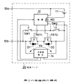
次に、本発明の第3の実施例を、図9を参照して説明する。この第3の実施例を適用した図9において、上述した第1の実施例を適用した図1に対応する部分には同一符号を付し、その詳細説明は省略する。
【0053】
本例の電池パック30は、制御回路12の+側の電源入力部と、二次電池11の正極側と端子10aとの間に、接続スイッチSW0を設けて、この接続スイッチSW0の制御を外部信号検出回路31の制御に基づいて行うようにしたものである。この場合、外部信号検出回路31は、端子10cから供給される制御信号の電圧Vaを検出して、充電状態を検出したとき、スイッチSW0及びSW1をオン状態とし、放電状態を検出したとき、スイッチSW0及びSW2をオン状態として、制御回路12に電源を供給するようにしたものである。
【0054】
その他の部分は、図1に示す第1の実施例の電池パックと同様に構成する。
【0055】
この図9に示す電池パック30として構成することで、上述した第1の実施例の場合と同様に、内蔵された二次電池11が過放電された場合でも、制御回路12に電源が供給されて、充電を行うことができる。そして、この第3の実施例に示す電池パック30の場合には、充電や放電をしない状態の場合には、制御回路12の電源入力部が、完全に回路から切り離されるので、例えば電池パック30の端子10a,10b間がショートするような事故があっても、制御回路12などを保護することができる。
【0056】
なお、この第3の実施例においても、充電開始時や放電開始時に、トランジスタFET1又はFET2をハイインピーダンス状態として、電池の状態を検出するようにしても良い。
【0057】
次に、本発明の第4の実施例を、図10を参照して説明する。この第4の実施例を適用した図10において、上述した第1,第2及び第3の実施例を適用した図1,図8及び図9に対応する部分には同一符号を付し、その詳細説明は省略する。
【0058】
図10に示す本例の電池パック40は、第2の実施例を適用した図8に示した電池パック20に、第3の実施例(図9)で説明したスイッチSW0を設けるようにしたものである。即ち、制御回路12の+側の電源入力部と、二次電池11の正極側と端子10aとの間に、接続スイッチSW0を設ける。そして、この接続スイッチSW0の制御を、電池パック40に内蔵された充放電検出回路41により行う。この充放電検出回路41は、端子10bとトランジスタFET1との接続点の電圧と、トランジスタFET2と抵抗器R0との接続点の電圧の電位差Vbの極性を検出するものである。この電位差Vbの極性として、トランジスタFET2側の電圧の方がトランジスタFET1側の電圧より高い場合には、充電状態であると検出する。また、電位差Vbの極性として、トランジスタFET1側の電圧の方がトランジスタFET2側の電圧より高い場合には、放電状態であると検出する。
【0059】
そして、検出した状態に基づいて、接続スイッチSW0,SW1,SW2の制御を行う。即ち、充放電検出回路41で充電状態を検出したとき、接続スイッチSW0及びSW1を接続状態とする。また、充放電検出回路41で放電状態を検出したとき、接続スイッチSW0及びSW2を接続状態とする。
【0060】
その他の部分は、図8に示す第2の実施例の電池パックと同様に構成する。
【0061】
この第2の実施例に示す電池パック40の場合には、上述した第2の実施例の場合と同様に、電池パックの内部で充電状態及び放電状態の検出を行うので、電池パックと接続される機器の双方の構成を簡単にすることができると共に、上述した第3の実施例の場合と同様に、電池パック40の端子10a,10b間がショートするような事故があっても、制御回路12などを保護することができる。
【0062】
なお、この第4の実施例においても、充電開始時や放電開始時に、トランジスタFET1又はFET2をハイインピーダンス状態として、電池の状態を検出するようにしても良い。
【0063】
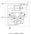
次に、本発明の第5の実施例を、図11を参照して説明する。この第5の実施例を適用した図11において、上述した第1及び第3の実施例を適用した図1及び図9に対応する部分には同一符号を付し、その詳細説明は省略する。
【0064】
図11に示す本例の電池パック50は、制御回路12への電源供給を制御するスイッチSW1及びSW2の代わりに、ダイオードを設けるようにしたものである。即ち、制御回路12の−側の電源入力部を、ダイオードD3及びD4のアノードに接続し、ダイオードD3のカソードを端子10bとトランジスタFET1との間に接続し、ダイオードD4のカソードをトランジスタFET2と抵抗器R0との間に接続する。
【0065】
そして、外部から端子10cに得られる信号を検出する外部信号検出回路51は、供給される信号の電圧Vaに基づいて充電状態及び放電状態の検出を行う回路で、充電状態又は放電状態の制御信号を検出したとき、スイッチSW0を接続状態として、制御回路12に電源を供給させる。この場合、充電時にはスイッチSW0とダイオードD3を介して電源が供給され、放電時にはスイッチSW0とダイオードD4を介して電源が供給されるようになる。そして、外部信号検出回路51で検出した充電状態又は放電状態の情報を、制御回路12に供給することで、制御回路12が対応した状態に基づいたトランジスタFET1,FET2の制御を行うことができる。
【0066】
その他の部分は、図9に示す第3の実施例の電池パックと同様に構成する。
【0067】
この第5の実施例の場合には、スイッチSW1及びSW2を設けないので、それだけ外部信号検出回路51で制御するスイッチとしてはスイッチSW0だけで良く、それだけスイッチを制御する構成を簡単にすることができる。なお、第1の実施例で説明したように、スイッチSW0を省略して、制御回路12の+側の電源入力部を直接的に二次電池11の正極側に接続するようにしても良い。
【0068】
なお、この第5の実施例においても、充電開始時や放電開始時に、トランジスタFET1又はFET2をハイインピーダンス状態として、電池の状態を検出するようにしても良い。
【0069】
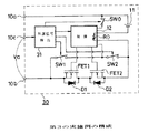
次に、本発明の第6の実施例を、図12を参照して説明する。この第6の実施例を適用した図12において、上述した第1,第2及び第5の実施例を適用した図1,図8及び図11に対応する部分には同一符号を付し、その詳細説明は省略する。
【0070】
図12に示す本例の電池パック60は、第5の実施例で説明したダイオードD3,D4をスイッチSW1,SW2の代わりに接続する構成を、第2の実施例で説明した充放電を内部で検出する電池パックに適用したものである。即ち、本例の電池パック60は、制御回路12の−側の電源入力部を、ダイオードD3及びD4のアノードに接続し、ダイオードD3のカソードを端子10bとトランジスタFET1との間に接続し、ダイオードD4のカソードをトランジスタFET2と抵抗器R0との間に接続する。
【0071】
そして、制御回路12の+側の電源入力部と、二次電池11の正極側と端子10aとの間に、接続スイッチSW0を設ける。そして、この接続スイッチSW0の制御を、電池パック60に内蔵された充放電検出回路61により行う。この充放電検出回路61は、端子10bとトランジスタFET1との接続点の電圧と、トランジスタFET2と抵抗器R0との接続点の電圧の電位差Vbの極性を検出するものである。この電位差Vbの極性として、トランジスタFET2側の電圧の方がトランジスタFET1側の電圧より高い場合には、充電状態であると検出する。また、電位差Vbの極性として、トランジスタFET1側の電圧の方がトランジスタFET2側の電圧より高い場合には、放電状態であると検出する。
【0072】
そして、検出した状態に基づいた情報を制御回路12に供給すると共に、充電状態又は放電状態のいずれかの状態を検出したとき、接続スイッチSW0を接続状態とする制御を行う。
【0073】
その他の部分は、図11に示す第5の実施例の電池パックと同様に構成する。
【0074】
この第6の実施例の場合にも、スイッチSW1及びSW2を設けないので、それだけ充放電検出回路61で制御するスイッチとしてはスイッチSW0だけで良く、それだけスイッチを制御する構成を簡単にすることができる。なお、第1の実施例で説明したように、スイッチSW0を省略して、制御回路12の+側の電源入力部を直接的に二次電池11の正極側に接続するようにしても良い。
【0075】
なお、この第6の実施例においても、充電開始時や放電開始時に、トランジスタFET1又はFET2をハイインピーダンス状態として、電池の状態を検出するようにしても良い。
【0076】
次に、本発明の第7の実施例を、図13及び図14を参照して説明する。この第7の実施例を適用した図13において、上述した第1及び第5の実施例を適用した図1及び図11に対応する部分には同一符号を付し、その詳細説明は省略する。
【0077】
図13に示す本例の電池パック70は、充放電制御用スイッチング手段である電界効果トランジスタが、制御回路12の電源供給用スイッチング手段も兼ねるようにしたものである。即ち、図13に示すように、−側の端子10bと二次電池11の負極側との間には、抵抗器R0と2個の電界効果トランジスタFET11 ,FET12 とが直列に接続してある。この場合、本例のトランジスタFET11 とFET12 の接続方向は、第1の実施例で説明したトランジスタFET1とFET2との接続方向とは逆方向にしてある。
【0078】
具体的には、二次電池11の負極側から順に、抵抗器R0,トランジスタFET12 ,トランジスタFET11 を介して端子10bに接続してあり、各トランジスタFET11 ,FET12 のソース・ドレイン間の接続方向としては、トランジスタFET11 は、制御回路12からゲートに得られる信号により、端子10bから二次電池11の方向への電流の流れを制限する状態に接続してある(制御回路12からのトランジスタFET11 の制御は第1の実施例でのトランジスタFET2の制御と同じ)。
【0079】
また、トランジスタFET12 は、制御回路12からゲートに得られる信号により、二次電池11から端子10bの方向への電流の流れを制限する状態に接続してある(制御回路12からのトランジスタFET12 の制御は第1の実施例でのトランジスタFET1の制御と同じ)。この場合、それぞれのトランジスタFET11 ,FET12 には、電流の流れが制限される方向とは反対方向に電流が流れる寄生ダイオードD11,D12がある状態となっている。
【0080】
そして、両トランジスタFET11 ,FET12 の接続中点を、制御回路12の−側の電源入力部と接続する。その他の部分は、図11に示す第5の実施例の電池パックと同様に構成する。
【0081】
ここで、この第7の実施例の構成での、充電時及び放電時の制御状態を、図13のフローチャートに基づいて説明する。まず、電池パック70が負荷装置又は充電器に接続されることで動作を開始し(ステップ301)、接続された場合には充電を行うモードであるのか、又は放電を行うモードであるのか(ステップ302)で、処理が異なる。
【0082】
まず、充電を行うモードである場合には、接続された充電器から充電を行うことを示す所定の電位の制御信号を発生させ、この制御信号を端子10cを介して電池パック10内の外部信号検出回路51に供給する(ステップ303)。そして、この制御信号を外部信号検出回路51で判別する(ステップ304)。このときには、充電状態に対応した電位が検出回路51で検出されるので、スイッチSW0をオン状態とする(ステップ305)。このスイッチSW0がオン状態となることで、接続された充電器側からの電源が電池パック70内の制御回路12に供給されるようになる。即ち、充電器側からの電源が、スイッチSW0とトランジスタFET11 の寄生ダイオードD11を介して制御回路12に供給されるようになる。そして、この電源の供給による制御回路12の作動で、検出回路51からの信号により充電が行われると判別される。
【0083】
この判別を行うと、制御回路12はトランジスタFET11 ,FET12 をオフ状態とする(ステップ306)。この状態で、二次電池11の電池電圧を制御回路12が検出し(ステップ307)、通常の充電が可能な電圧(基準電圧)以上あるか否か判断する(ステップ308)。そして、基準電圧以上ある場合には、トランジスタFET12 をオン状態として(ステップ310)、充電を開始させる(ステップ311)。このときには、充電電流が寄生ダイオードD11とトランジスタFET12 を流れるようになる。
【0084】
そして、ステップ308で検出した電圧値が基準電圧未満の場合には、トランジスタFET12 をハイインピーダンス状態とする(ステップ309)。この状態でステップ307での電池電圧の検出を行い、ステップ308の判断で二次電池11の電池電圧が基準電圧以上になった場合には、ステップ310に移って充電を開始させる。
【0085】
次にステップ302で放電を行うモードである場合には、接続された負荷装置から放電を行うことを示す所定の電位の制御信号を発生させ、この制御信号を端子10cを介して電池パック10内の外部信号検出回路51に供給する(ステップ312)。そして、この制御信号を外部信号検出回路51で判別する(ステップ313)。このときには、放電状態に対応した電位が検出回路51で検出されるので、スイッチSW0をオン状態とする(ステップ314)。このスイッチSW0がオン状態となることで、二次電池11からの電源が制御回路12に供給されるようになる。即ち、二次電池11からの電源が、スイッチSW0とトランジスタFET12 の寄生ダイオードD12を介して制御回路12に供給されるようになる。そして、この電源の供給による制御回路12の作動で、検出回路51からの信号により充電が行われると判別される。
【0086】
この判別を行うと、制御回路12はトランジスタFET11 をハイインピーダンス状態とすると共に、トランジスタFET12 をオン状態とする(ステップ315)。この状態で、二次電池11の出力電圧を制御回路12が検出し(ステップ316)、出力電圧が放電するのに適した電圧(基準電圧)以上であるか否か判断する(ステップ317)。ここで、検出した電圧値が基準電圧以上である場合には、トランジスタFET11 をオン状態とすると共に、トランジスタFET12 をオフ状態とし(ステップ218)、放電を開始させる(ステップ219)。
【0087】
そして、ステップ217で検出した電圧が基準電圧未満の場合には、所定時間電圧の変化を監視した後(ステップ220)、トランジスタFET1及びFET2をオフ状態として、放電を停止させる(ステップ221)。
【0088】
この第7の実施例の場合には、上述した第5の実施例の場合と同様に、スイッチSW1及びSW2を設けないので、それだけ充放電検出回路51で制御するスイッチとしてはスイッチSW0だけで良く、それだけスイッチを制御する構成を簡単にすることができると共に、ダイオードD3,D4についてもトランジスタの寄生ダイオードD11,D12で兼用させたので、より構成を簡単にすることができる。なお、この例でも第1の実施例で説明したように、スイッチSW0を省略して、制御回路12の+側の電源入力部を直接的に二次電池11の正極側に接続するようにしても良い。
【0089】
次に、本発明の第8の実施例を、図15を参照して説明する。この第8の実施例を適用した図15において、上述した第1,第6及び第7の実施例を適用した図1,図12及び図13に対応する部分には同一符号を付し、その詳細説明は省略する。
【0090】
図15に示す本例の電池パック80は、第7の実施例と同様に充放電制御用スイッチング手段である電界効果トランジスタが、制御回路12の電源供給用スイッチング手段も兼ねるようにしたもので、その場合に第6の実施例のように電池パック内の充放電検出回路61で充放電状態を検出するようにしたものである。即ち、図15に示すように、−側の端子10bと二次電池11の負極側との間には、抵抗器R0と2個の電界効果トランジスタFET11 ,FET12 とが直列に接続してある。この場合、本例のトランジスタFET11 とFET12 の接続方向は、第1の実施例で説明したトランジスタFET1とFET2との接続方向とは逆方向にしてある。
【0091】
そして、充放電検出回路61で、端子10bとトランジスタFET1との接続点の電圧と、トランジスタFET2と抵抗器R0との接続点の電圧の電位差Vbの極性を検出する。この電位差Vbの極性として、トランジスタFET12 側の電圧の方がトランジスタFET11 側の電圧より高い場合には、充電状態であると検出する。また、電位差Vbの極性として、トランジスタFET11 側の電圧の方がトランジスタFET12 側の電圧より高い場合には、放電状態であると検出する。
【0092】
そして、検出した状態に基づいた情報を制御回路12に供給すると共に、充電状態又は放電状態のいずれかの状態を検出したとき、接続スイッチSW0を接続状態とする制御を行う。
【0093】
その他の部分は、図13に示す第7の実施例の電池パックと同様に構成する。
【0094】
この第8の実施例の場合には、上述した第7の実施例の場合と同様に、スイッチSW1及びSW2を設けないので、それだけ充放電検出回路51で制御するスイッチとしてはスイッチSW0だけで良く、それだけスイッチを制御する構成を簡単にすることができると共に、ダイオードD3,D4についてもトランジスタの寄生ダイオードD11,D12で兼用させたので、より構成を簡単にすることができる。そして更に、電池パック内部で充放電状態の検出を行うようにしたので、この点からも電池パックの構成を簡単にすることができる。なお、この例でも第1の実施例で説明したように、スイッチSW0を省略して、制御回路12の+側の電源入力部を直接的に二次電池11の正極側に接続するようにしても良い。
【0095】
なお、上述した各実施例においては、電池パック内に内蔵させる二次電池としてリチウムイオン電池を適用するようにしたが、その他の構造の二次電池を内蔵させるようにしても良い。
【0096】
【発明の効果】
本発明によると、充電時には外部からの電源で保護回路を構成する制御手段に電源が供給されるので、内蔵された二次電池の残量の有無にかかわらず充電動作が可能になる。そして、放電時には内蔵された二次電池から制御手段に電源が供給され、放電動作についても良好に行うことが可能になる。
【0097】
この場合、検出手段での検出状態に応じて制御される別のスイッチ(実施例でのスイッチSW0)を設けることで、制御手段を作動させないときには、制御手段を端子側から完全に切り離すことができ、端子部のショートなどがあっても、制御手段を損傷させることがなくなる。
【0098】
また、状態検出手段で、外部から得られる信号を検出して、充放電状態の検出を行うようにしたことで、外部からの制御に基づいて、良好に充電と放電の制御が可能になる。
【0099】
また、状態検出手段で、一方の端子部と二次電池の一方の極との間に生じる電位差の極性を検出して、充放電状態の検出を行うようにしたことで、電池パックの内部での検出処理で充電状態や放電状態の検出ができ、外部から制御信号などを供給する必要がなくなり、簡単な構成で実現できるようになる。
【0100】
また、充放電制御用スイッチング手段として、二次電池の充電方向の電流をスイッチングする第1の充放電制御用スイッチング手段と、二次電池の放電方向の電流をスイッチングする第2の充放電制御用スイッチング手段とで構成したことで、2個の電界効果トランジスタなどのスイッチング手段を使用して、良好に充電と放電の制御ができるようになる。
【0101】
また、この場合に状態検出手段で充電状態を検出したとき、第1の充放電制御用スイッチング手段をハイインピーダンス状態として電池電圧を検出した後、第1の充放電制御用スイッチング手段をオン状態として充電を行い、状態検出手段で放電状態を検出したとき、第2の充放電制御用スイッチング手段をハイインピーダンス状態として出力電圧を検出した後、第2の充放電制御用スイッチング手段をオン状態として放電を行うようにしたことで、電池の状態を正確に判断して充電や放電を行うことが可能になり、過放電や過充電などを良好に防止することができる。
【0102】
また、第1及び第2の制御手段電源供給用スイッチング手段の代わりに、ダイオードを接続したことで、スイッチング手段を制御する必要がなくなり、構成を簡単にすることができる。
【図面の簡単な説明】
【図1】本発明の第1の実施例の構成を示す構成図である。
【図2】第1の実施例による充放電開始時の処理を示すフローチャートである。
【図3】第1の実施例の具体回路例を示す回路図である。
【図4】第1の実施例による充放電開始時の処理(インピーダンス制御時)を示すフローチャートである。
【図5】二次電池の放電時の特性を示す特性図である。
【図6】第1の実施例においてトランジスタをスイッチング動作させる場合の状態を示すタイミング図である。
【図7】実施例による電池パックを接続した例を示す構成図である。
【図8】本発明の第2の実施例の構成を示す構成図である。
【図9】本発明の第3の実施例の構成を示す構成図である。
【図10】本発明の第4の実施例の構成を示す構成図である。
【図11】本発明の第5の実施例の構成を示す構成図である。
【図12】本発明の第6の実施例の構成を示す構成図である。
【図13】本発明の第7の実施例の構成を示す構成図である。
【図14】第7の実施例による充放電開始時の処理を示すフローチャートである。
【図15】本発明の第8の実施例の構成を示す構成図である。
【図16】従来の電池パックの構成の一例を示す構成図である。
【符号の説明】
10,20,30,40,50,60,70,80 電池パック
10a +側端子
10b −側端子
11 二次電池
12 制御回路
13,31,51 外部信号検出回路
14,41,61 充放電検出回路
FET1,FET2,FET11 ,FET12 電界効果トランジスタ
D1,D2,D11,D12 寄生ダイオード
SW0,SW1,SW2 スイッチ[0001]
[Technical field to which the invention belongs]
The present invention relates to a secondary battery pack that houses a secondary battery such as a lithium ion battery and is connected to a load device or a charger.
[0002]
[Prior art]
A secondary battery, which is a rechargeable battery, may be used by being housed in a casing called a battery pack. The battery pack is stored in a state where a predetermined number of secondary batteries are connected in series or in parallel so that a predetermined battery capacity can be obtained in advance (in some cases, only one secondary battery is stored). The secondary battery protection circuit is built in to prevent overcharge and overdischarge of the secondary battery and to prevent damage to the secondary battery due to a short circuit of the terminal portion.
[0003]
FIG. 16 is a diagram showing a battery pack containing a conventional secondary battery. The
[0004]
The
[0005]
With this configuration, when a charging device (not shown) is connected to the
[0006]
When the
[0007]
Thus, by connecting two field effect transistors FET1 and FET2 in series and performing the control based on the determination of the charge / discharge state, the
[0008]
[Problems to be solved by the invention]
By the way, the
[0009]
For example, it is assumed that the
[0010]
In such a situation, even if the
[0011]
In addition to the case where the battery is overdischarged in this way, the
[0012]
In view of these points, it is an object of the present invention to make a secondary battery usable even when an undesirable state such as overdischarge occurs.
[0013]
[Means for Solving the Problems]
In order to solve this problem, the present invention is connected between the terminal portion of the battery pack and the control means. When the detection means detects that the secondary battery is in a charged state, it is turned on. The first control means is connected between the power supply switching means, the electrode of the secondary battery and the control means. When the detection means detects that the secondary battery is in a discharged state, it is turned on. The second control means includes power supply switching means.
[0014]
According to such a configuration, the control means can be operated by the power supplied from the external charging device side by turning on the first control means power supply switching means at the time of charging. The switching means for discharging control can be controlled, and the charging operation can be performed regardless of the remaining amount of the secondary battery.
[0015]
In addition, when discharging, the second control means power supply switching means is turned on so that the control means can be operated by the power source from the secondary battery, and this control means controls the charge / discharge control switching means. The discharge operation is possible regardless of the state of the terminal portion of the battery pack.
[0016]
DETAILED DESCRIPTION OF THE INVENTION
A first embodiment of the present invention will be described below with reference to FIGS.
[0017]
FIG. 1 is a block diagram showing the configuration of the battery pack of this example. The
[0018]
The
[0019]
The external
[0020]
When the external
[0021]
By being controlled in this way, when the
[0022]
The
[0023]
Next, the operation at the time of charging and discharging of the
[0024]
First, in the charging mode, a control signal having a predetermined potential indicating that charging is performed is generated from the connected charger, and this control signal is output to an external signal in the
[0025]
Then, after the start of charging, the
[0026]
Next, in
[0027]
When the
[0028]
By performing the control at the time of charging and the control at the time of discharging in this way, the
[0029]
Although a specific configuration for controlling the switches SW1 and SW2 is not described in FIG. 1, various switch control methods based on voltage detection can be applied. For example, a configuration in which a Zener diode and a transistor are combined may be used. That is, as shown in FIG. 3, the terminal 10c is connected to the terminal 10b through a series circuit of a Zener diode ZD1 and a resistor R1, and the midpoint of connection between the Zener diode ZD1 and the resistor R1 is defined as an NPN transistor Q1. Connect to the base of the. The emitter of the transistor Q1 is connected between the transistor FET1 and the terminal 10b. Further, the terminal 10c is connected between the transistor FET2 and the resistor R0 through a series circuit of the Zener diode ZD2 and the resistor R2, and the midpoint of connection between the Zener diode ZD2 and the resistor R2 is an NPN transistor. Connect to the base of Q2. The emitter of the transistor Q2 is connected between the transistor FET2 and the resistor R0. Then, the collectors of the transistors Q1 and Q2 are connected to the power supply input section on the negative side of the
[0030]
Here, the resistance values of the resistors R1 and R2 are set corresponding to the voltage of the control signal obtained at the terminal 10c during charging and discharging, respectively.
[0031]
With this configuration, the transistors Q1 and Q2 function as the switches SW1 and SW2. That is, when a control signal having a potential indicating charging is supplied to the terminal 10c, the transistor Q1 is turned on so that power is supplied to the
[0032]
In the example of FIG. 3, the configuration for supplying the control signal obtained at the terminal 10c to the
[0033]
In the configuration described above, the
[0034]
An example of processing when the state of the
[0035]
First, in the charging mode, a control signal having a predetermined potential indicating that charging is performed is generated from the connected charger, and this control signal is output to an external signal in the
[0036]
When this determination is made, the
[0037]
When a battery voltage equal to or higher than the reference voltage is detected in
[0038]
Next, in the case of the discharge mode in
[0039]
When this determination is made, the
[0040]
If the voltage detected in
[0041]
For monitoring the voltage change in
[0042]
Before charging or discharging is performed in this way, the state of the
[0043]
Instead of setting the transistor FET1 or FET2 to the high impedance state, the corresponding transistor FET1 or FET2 may be periodically turned on / off to be substantially the same as the high impedance state. That is, for example, as shown in FIG. 6 (the period in which the pulse of FIG. 6 rises is in the on state and the period in which the pulse has fallen indicates the off state) It can be controlled to the same state.
[0044]
Next, the connection state of the
[0045]
By adopting such a configuration, for example, when the remaining amount of the
[0046]
Next, a second embodiment of the present invention will be described with reference to FIG. In FIG. 8 to which the second embodiment is applied, the same reference numerals are given to the portions corresponding to those in FIG. 1 to which the first embodiment is applied, and the detailed description thereof is omitted.
[0047]
In this example, the charge state and the discharge state are detected in the battery pack, and it is not necessary to supply a charge / discharge control signal from the outside, and the configuration is as shown in FIG. The battery pack 20 in this example is provided with a charge /
[0048]
Based on the detected state, the connection switches SW1 and SW2 are controlled. That is, when the charge /
[0049]
Other parts are configured in the same manner as the battery pack of the first embodiment shown in FIG.
[0050]
In the case of the battery pack 20 shown in the second embodiment, since the charge state and the discharge state are detected inside the battery pack, it is not necessary to supply a control signal for charge or discharge from the outside, and only the battery pack 20 is connected. Device (load device or charger) side can be simplified, and the terminal for receiving the control signal (terminal 10c in FIG. 1) is not necessary on the battery pack 20 side, and the configuration on the battery pack side is also simple. become.
[0051]
In the second embodiment, the state of the battery may be detected by setting the transistor FET1 or FET2 in a high impedance state at the start of charging or discharging.
[0052]
Next, a third embodiment of the present invention will be described with reference to FIG. In FIG. 9 to which the third embodiment is applied, the same reference numerals are given to the portions corresponding to FIG. 1 to which the first embodiment described above is applied, and the detailed description thereof is omitted.
[0053]
In the
[0054]
Other parts are configured in the same manner as the battery pack of the first embodiment shown in FIG.
[0055]
By configuring as the
[0056]
In the third embodiment, the state of the battery may be detected by setting the transistor FET1 or FET2 to the high impedance state at the start of charging or discharging.
[0057]
Next, a fourth embodiment of the present invention will be described with reference to FIG. In FIG. 10 to which the fourth embodiment is applied, parts corresponding to those in FIGS. 1, 8 and 9 to which the first, second and third embodiments are applied are denoted by the same reference numerals. Detailed description is omitted.
[0058]
In the
[0059]
Based on the detected state, the connection switches SW0, SW1, and SW2 are controlled. That is, when the charge /
[0060]
Other parts are configured in the same manner as the battery pack of the second embodiment shown in FIG.
[0061]
In the case of the
[0062]
In the fourth embodiment, the state of the battery may be detected by setting the transistor FET1 or FET2 to a high impedance state at the start of charging or discharging.
[0063]
Next, a fifth embodiment of the present invention will be described with reference to FIG. In FIG. 11 to which the fifth embodiment is applied, the same reference numerals are given to the portions corresponding to FIGS. 1 and 9 to which the first and third embodiments described above are applied, and the detailed description thereof is omitted.
[0064]
The
[0065]
An external
[0066]
Other parts are configured in the same manner as the battery pack of the third embodiment shown in FIG.
[0067]
In the case of the fifth embodiment, since the switches SW1 and SW2 are not provided, the switch controlled by the external
[0068]
In the fifth embodiment, the state of the battery may be detected by setting the transistor FET1 or FET2 to the high impedance state at the start of charging or discharging.
[0069]
Next, a sixth embodiment of the present invention will be described with reference to FIG. In FIG. 12 to which the sixth embodiment is applied, parts corresponding to those in FIGS. 1, 8 and 11 to which the first, second and fifth embodiments are applied are denoted by the same reference numerals, Detailed description is omitted.
[0070]
The battery pack 60 of this example shown in FIG. 12 has a configuration in which the diodes D3 and D4 described in the fifth example are connected instead of the switches SW1 and SW2, and the charge / discharge described in the second example is internally performed. This is applied to the battery pack to be detected. That is, in the battery pack 60 of this example, the negative power input portion of the
[0071]
Then, a connection switch SW0 is provided between the power input part on the + side of the
[0072]
Then, information based on the detected state is supplied to the
[0073]
Other parts are configured in the same manner as the battery pack of the fifth embodiment shown in FIG.
[0074]
Also in the case of the sixth embodiment, since the switches SW1 and SW2 are not provided, the switch SW0 is only required to be controlled by the charge /
[0075]
In the sixth embodiment, the state of the battery may be detected by setting the transistor FET1 or FET2 in a high impedance state at the start of charging or discharging.
[0076]
Next, a seventh embodiment of the present invention will be described with reference to FIGS. In FIG. 13 to which the seventh embodiment is applied, portions corresponding to those in FIGS. 1 and 11 to which the first and fifth embodiments are applied are denoted by the same reference numerals, and detailed description thereof is omitted.
[0077]
The
[0078]
Specifically, in order from the negative electrode side of the
[0079]
The transistor FET12 is connected to a state in which the current flow from the
[0080]
Then, the midpoint of connection between the transistors FET11 and FET12 is connected to the negative side power input section of the
[0081]
Here, the control state at the time of charging and discharging in the configuration of the seventh embodiment will be described based on the flowchart of FIG. First, the operation starts when the
[0082]
First, in the charging mode, a control signal having a predetermined potential indicating that charging is performed is generated from the connected charger, and this control signal is output to an external signal in the
[0083]
When this determination is made, the
[0084]
If the voltage value detected in
[0085]
Next, in the case of the discharge mode in
[0086]
When this determination is made, the
[0087]
If the voltage detected in
[0088]
In the case of the seventh embodiment, as in the case of the fifth embodiment described above, the switches SW1 and SW2 are not provided, so that the switch SW0 is the only switch controlled by the charge /
[0089]
Next, an eighth embodiment of the present invention will be described with reference to FIG. In FIG. 15 to which the eighth embodiment is applied, parts corresponding to those in FIGS. 1, 12, and 13 to which the first, sixth, and seventh embodiments are applied are denoted by the same reference numerals. Detailed description is omitted.
[0090]
The battery pack 80 of this example shown in FIG. 15 is such that the field effect transistor, which is the switching means for charge / discharge control, also serves as the power supply switching means of the
[0091]
The charge /
[0092]
Then, information based on the detected state is supplied to the
[0093]
Other parts are configured in the same manner as the battery pack of the seventh embodiment shown in FIG.
[0094]
In the case of the eighth embodiment, as in the case of the seventh embodiment described above, the switches SW1 and SW2 are not provided, so that the switch SW0 is the only switch controlled by the charge /
[0095]
In each of the above-described embodiments, the lithium ion battery is applied as the secondary battery incorporated in the battery pack. However, a secondary battery having another structure may be incorporated.
[0096]
【The invention's effect】
According to the present invention, since the power is supplied to the control means that constitutes the protection circuit with an external power source during charging, the charging operation can be performed regardless of whether or not the built-in secondary battery is remaining. In discharging, power is supplied to the control means from the built-in secondary battery, and the discharging operation can be performed well.
[0097]
In this case, by providing another switch (switch SW0 in the embodiment) that is controlled according to the detection state of the detection means, the control means can be completely disconnected from the terminal side when the control means is not operated. Even if there is a short circuit of the terminal portion, the control means is not damaged.
[0098]
Further, since the state detection means detects the signal obtained from the outside and detects the charge / discharge state, the charge and discharge can be controlled satisfactorily based on the control from the outside.
[0099]
In addition, the state detection means detects the polarity of the potential difference generated between one terminal portion and one electrode of the secondary battery, and detects the charge / discharge state. In this detection process, the state of charge or discharge can be detected, and it is not necessary to supply a control signal or the like from the outside, which can be realized with a simple configuration.
[0100]
Moreover, as the switching means for charge / discharge control, the first charge / discharge control switching means for switching the current in the charge direction of the secondary battery, and the second charge / discharge control for switching the current in the discharge direction of the secondary battery. By using the switching means, it is possible to satisfactorily control charging and discharging by using switching means such as two field effect transistors.
[0101]
In this case, when the state detection unit detects the state of charge, the first charge / discharge control switching unit is set to the high impedance state, the battery voltage is detected, and then the first charge / discharge control switching unit is turned on. When charging is performed and the discharge state is detected by the state detection unit, the second charge / discharge control switching unit is set to the high impedance state, the output voltage is detected, and then the second charge / discharge control switching unit is turned on to discharge. By performing the above, it becomes possible to accurately determine the state of the battery and perform charging and discharging, and it is possible to satisfactorily prevent overdischarge and overcharge.
[0102]
Further, since the diode is connected instead of the first and second control means power supply switching means, it is not necessary to control the switching means, and the configuration can be simplified.
[Brief description of the drawings]
FIG. 1 is a configuration diagram showing a configuration of a first exemplary embodiment of the present invention.
FIG. 2 is a flowchart showing processing at the start of charging / discharging according to the first embodiment.
FIG. 3 is a circuit diagram showing a specific circuit example of the first embodiment;
FIG. 4 is a flowchart showing processing (impedance control) at the start of charge / discharge according to the first embodiment;
FIG. 5 is a characteristic diagram showing characteristics of the secondary battery during discharging.
FIG. 6 is a timing chart showing a state in which a transistor is switched in the first embodiment.
FIG. 7 is a configuration diagram showing an example in which a battery pack according to an embodiment is connected.
FIG. 8 is a configuration diagram showing a configuration of a second exemplary embodiment of the present invention.
FIG. 9 is a configuration diagram showing a configuration of a third exemplary embodiment of the present invention.
FIG. 10 is a configuration diagram showing a configuration of a fourth exemplary embodiment of the present invention.
FIG. 11 is a configuration diagram showing the configuration of a fifth exemplary embodiment of the present invention.
FIG. 12 is a block diagram showing the configuration of a sixth embodiment of the present invention.
FIG. 13 is a configuration diagram showing a configuration of a seventh exemplary embodiment of the present invention.
FIG. 14 is a flowchart showing processing at the start of charging / discharging according to the seventh embodiment.
FIG. 15 is a block diagram showing the configuration of an eighth embodiment of the present invention.
FIG. 16 is a configuration diagram showing an example of a configuration of a conventional battery pack.
[Explanation of symbols]
10, 20, 30, 40, 50, 60, 70, 80 Battery pack
10a + side terminal
10b-side terminal
11 Secondary battery
12 Control circuit
13, 31, 51 External signal detection circuit
14, 41, 61 Charge / discharge detection circuit
FET1, FET2, FET11, FET12 field effect transistor
D1, D2, D11, D12 Parasitic diode
SW0, SW1, SW2 switch
Claims (5)
所定の状態で収納され上記一方の端子部と一方の極とが接続された二次電池と、
上記他方の端子部と上記二次電池の他方の極との間に直列に接続される充放電制御用スイッチング手段と、
上記二次電池の充放電状態を検出する状態検出手段と、
上記検出手段での検出状態に応じて上記充放電制御用スイッチング手段を制御する制御手段とを備えた二次電池パックにおいて、
上記一方の端子部と上記制御手段とを接続し、
上記他方の端子部と上記制御手段との間に接続され、上記検出手段において上記二次電池が充電状態であることを検出した時はオン状態とする第1の制御手段電源供給用スイッチング手段と、
上記二次電池の他方の極と上記制御手段との間に接続され、上記検出手段において上記二次電池が放電状態であることを検出した時はオン状態とする第2の制御手段電源供給用スイッチング手段とを備え、
上記状態検出手段で、外部から得られる信号を検出して、充放電状態の検出を行うようにした
二次電池パック。One and the other terminal connected to the load device or the charging device;
A secondary battery stored in a predetermined state and connected to the one terminal portion and the one pole;
Switching means for charge / discharge control connected in series between the other terminal portion and the other electrode of the secondary battery;
State detecting means for detecting a charge / discharge state of the secondary battery;
In a secondary battery pack comprising a control means for controlling the charge / discharge control switching means according to the detection state of the detection means,
Connecting the one terminal part and the control means;
A first control unit that is connected between the other terminal and the control unit and is turned on when the detection unit detects that the secondary battery is in a charged state; ,
Second control means connected between the other electrode of the secondary battery and the control means, and turned on when the detection means detects that the secondary battery is in a discharged state. Switching means,
A secondary battery pack in which the state detection means detects a signal obtained from the outside to detect a charge / discharge state.
所定の状態で収納され上記一方の端子部と一方の極とが接続された二次電池と、
上記他方の端子部と上記二次電池の他方の極との間に直列に接続される充放電制御用スイッチング手段と、
上記二次電池の充放電状態を検出する状態検出手段と、
上記検出手段での検出状態に応じて上記充放電制御用スイッチング手段を制御する制御手段とを備えた二次電池パックにおいて、
上記一方の端子部と上記制御手段とを接続し、
上記他方の端子部と上記制御手段との間に接続され、上記検出手段において上記二次電池が充電状態であることを検出した時はオン状態とする第1の制御手段電源供給用スイッチング手段と、
上記二次電池の他方の極と上記制御手段との間に接続され、上記検出手段において上記二次電池が放電状態であることを検出した時はオン状態とする第2の制御手段電源供給用スイッチング手段とを備え、
上記充放電制御用スイッチング手段として、
上記二次電池の充電方向の電流をスイッチングする第1の充放電制御用スイッチング手段と、
上記二次電池の放電方向の電流をスイッチングする第2の充放電制御用スイッチング手段とで構成した
二次電池パック。One and the other terminal connected to the load device or the charging device;
A secondary battery stored in a predetermined state and connected to the one terminal portion and the one pole;
Switching means for charge / discharge control connected in series between the other terminal portion and the other electrode of the secondary battery;
State detecting means for detecting a charge / discharge state of the secondary battery;
In a secondary battery pack comprising a control means for controlling the charge / discharge control switching means according to the detection state of the detection means,
Connecting the one terminal part and the control means;
A first control unit that is connected between the other terminal and the control unit and is turned on when the detection unit detects that the secondary battery is in a charged state; ,
Second control means connected between the other electrode of the secondary battery and the control means, and turned on when the detection means detects that the secondary battery is in a discharged state. Switching means,
As the charge / discharge control switching means,
First charging / discharging control switching means for switching a current in a charging direction of the secondary battery;
The secondary battery pack comprised with the switching means for the 2nd charge / discharge control which switches the electric current of the discharge direction of the said secondary battery.
それぞれ電界効果トランジスタを使用した
請求項2記載の二次電池パック。As the first and second charge / discharge control switching means,
The secondary battery pack according to claim 2, wherein each uses a field effect transistor.
上記状態検出手段で充電状態を検出したとき、上記第1の充放電制御用スイッチング手段をハイインピーダンス状態として、上記電圧検出手段で所定電圧以上の電圧の検出により、上記第1の充放電制御用スイッチング手段をオン状態として充電を行い、
上記状態検出手段で放電状態を検出したとき、上記第2の充放電制御用スイッチング手段をハイインピーダンス状態として、上記電圧検出手段で所定電圧以上の電圧の検出により、上記第2の充放電制御用スイッチング手段をオン状態として放電を行うようにした
請求項2記載の二次電池パック。A voltage detection means between one electrode and the other electrode of the secondary battery,
When the charging state is detected by the state detecting unit, the first charging / discharging control switching unit is set to a high impedance state, and the voltage detecting unit detects a voltage equal to or higher than a predetermined voltage to detect the first charging / discharging control. Charging with the switching means turned on,
When the discharge state is detected by the state detection unit, the second charge / discharge control switching unit is set to a high impedance state, and the voltage detection unit detects a voltage equal to or higher than a predetermined voltage to detect the second charge / discharge control. The secondary battery pack according to claim 2, wherein discharging is performed with the switching means turned on.
請求項1記載の二次電池パック。When the first and second control means are connected between the other terminal part and the control means as the power supply switching means, and the detection means detects that the secondary battery is in a charged state. Is connected between the control means and the first control means power supply diode to be turned on, and the other end of the resistor connected to the other end of the secondary battery and one end. When the detection means detects that the secondary battery is in a discharged state, and includes a second control means power supply diode that is turned on, and when the secondary battery detects that the secondary battery is in a discharged state The secondary battery pack according to claim 1, wherein a second control means power supply diode to be turned on is connected.
Priority Applications (4)
| Application Number | Priority Date | Filing Date | Title |
|---|---|---|---|
| JP29144295A JP3713770B2 (en) | 1995-11-09 | 1995-11-09 | Secondary battery pack |
| TW085113563A TW310483B (en) | 1995-11-09 | 1996-11-06 | |
| US08/743,809 US5783322A (en) | 1995-11-09 | 1996-11-06 | Secondary battery pack |
| KR1019960053001A KR100415763B1 (en) | 1995-11-09 | 1996-11-08 | Rechargeable battery pack |
Applications Claiming Priority (1)
| Application Number | Priority Date | Filing Date | Title |
|---|---|---|---|
| JP29144295A JP3713770B2 (en) | 1995-11-09 | 1995-11-09 | Secondary battery pack |
Publications (2)
| Publication Number | Publication Date |
|---|---|
| JPH09140066A JPH09140066A (en) | 1997-05-27 |
| JP3713770B2 true JP3713770B2 (en) | 2005-11-09 |
Family
ID=17768929
Family Applications (1)
| Application Number | Title | Priority Date | Filing Date |
|---|---|---|---|
| JP29144295A Expired - Fee Related JP3713770B2 (en) | 1995-11-09 | 1995-11-09 | Secondary battery pack |
Country Status (4)
| Country | Link |
|---|---|
| US (1) | US5783322A (en) |
| JP (1) | JP3713770B2 (en) |
| KR (1) | KR100415763B1 (en) |
| TW (1) | TW310483B (en) |
Families Citing this family (49)
| Publication number | Priority date | Publication date | Assignee | Title |
|---|---|---|---|---|
| US5742148A (en) * | 1992-11-24 | 1998-04-21 | Seiko Instruments Inc. | Charge/discharge control circuit and chargeable electric power source apparatus |
| US5936384A (en) * | 1997-06-09 | 1999-08-10 | Ricoh Company, Ltd. | Charge and discharge protection circuit and battery pack with high withstand voltage |
| US5883495A (en) * | 1997-07-31 | 1999-03-16 | National Semiconductor Corporation | Bidirectional current control circuit suitable for controlling the charging and discharging of rechargeable battery cells |
| US6451463B1 (en) * | 1997-10-06 | 2002-09-17 | Reveo, Inc. | Electro-chemical power generation systems employing arrays of electronically-controllable discharging and/or recharging cells within a unity support structure |
| JPH11215728A (en) * | 1998-01-28 | 1999-08-06 | Sanyo Electric Co Ltd | Charging circuit and pack battery |
| US6163131A (en) * | 1998-04-02 | 2000-12-19 | The Procter & Gamble Company | Battery having a built-in controller |
| US6118248A (en) * | 1998-04-02 | 2000-09-12 | The Procter & Gamble Company | Battery having a built-in controller to extend battery service run time |
| US6198250B1 (en) | 1998-04-02 | 2001-03-06 | The Procter & Gamble Company | Primary battery having a built-in controller to extend battery run time |
| US6835491B2 (en) | 1998-04-02 | 2004-12-28 | The Board Of Trustees Of The University Of Illinois | Battery having a built-in controller |
| US6074775A (en) * | 1998-04-02 | 2000-06-13 | The Procter & Gamble Company | Battery having a built-in controller |
| US6100670A (en) * | 1998-04-14 | 2000-08-08 | Conexant Systems, Inc. | Multi-functional battery management module operable in a charging mode and a battery pack mode |
| US6331763B1 (en) * | 1998-04-15 | 2001-12-18 | Tyco Electronics Corporation | Devices and methods for protection of rechargeable elements |
| DE19837909C2 (en) * | 1998-08-20 | 2001-05-17 | Implex Hear Tech Ag | Protection device for a multi-rechargeable electrochemical battery |
| JP3747647B2 (en) * | 1998-09-09 | 2006-02-22 | ミツミ電機株式会社 | Secondary battery protection circuit |
| JP3358559B2 (en) * | 1998-10-01 | 2002-12-24 | ミツミ電機株式会社 | Low power consumption circuit and secondary battery protection circuit |
| TW468295B (en) * | 1999-04-15 | 2001-12-11 | Seiko Instr Inc | Charge/discharge controlling semiconductor device |
| US9397370B2 (en) | 1999-06-25 | 2016-07-19 | The Board Of Trustees Of The University Of Illinois | Single and multiple cell battery with built-in controller |
| JP3935922B2 (en) | 1999-12-03 | 2007-06-27 | 富士通株式会社 | Secondary battery charge / discharge control circuit |
| JP4126144B2 (en) * | 2000-05-11 | 2008-07-30 | インターナショナル・ビジネス・マシーンズ・コーポレーション | Charging system, intelligent battery, and charging method |
| JP3445561B2 (en) | 2000-07-17 | 2003-09-08 | 株式会社東芝 | Computer system |
| WO2002071734A2 (en) * | 2000-12-19 | 2002-09-12 | Smal Camera Technologies, Inc. | Compact digital camera system |
| WO2004040761A1 (en) * | 2002-10-29 | 2004-05-13 | Koninklijke Philips Electronics N.V. | Bi-directional double nmos switch |
| AU2003901730A0 (en) * | 2003-04-11 | 2003-05-01 | Cochlear Limited | Power management system |
| US7605565B2 (en) * | 2003-12-05 | 2009-10-20 | Hewlett-Packard Development Company, L.P. | Battery pack with protection circuit |
| JP2006034032A (en) * | 2004-07-20 | 2006-02-02 | Ricoh Co Ltd | Battery pack having secondary battery and charging system device using the battery pack |
| US8004237B2 (en) * | 2005-03-11 | 2011-08-23 | Techtium , Ltd. | Battery power supply with bidirectional battery charge controller |
| JP2006331953A (en) * | 2005-05-27 | 2006-12-07 | Mitsumi Electric Co Ltd | Battery protection method and battery protection circuit |
| US7595610B2 (en) * | 2005-11-23 | 2009-09-29 | Micropower Electronics Inc. | Redundant battery protection system and method |
| JP2007200758A (en) * | 2006-01-27 | 2007-08-09 | Toshiba Corp | Battery pack |
| US7605568B2 (en) * | 2006-03-10 | 2009-10-20 | Atmel Corporation | Deep under voltage recovery in a battery pack |
| KR100927246B1 (en) * | 2006-09-11 | 2009-11-16 | 주식회사 엘지화학 | Electrode mixture containing clay mineral and electrochemical cell using the same |
| US20090047572A1 (en) * | 2007-08-16 | 2009-02-19 | Micropower Electronics, Inc. | Controlled pressure release for packaged batteries and associated systems and methods |
| TWI416788B (en) * | 2010-11-03 | 2013-11-21 | Ind Tech Res Inst | Fuel cell system |
| JP5747491B2 (en) | 2010-12-08 | 2015-07-15 | ソニー株式会社 | Electric storage system, electric vehicle and electric power system |
| JP2013102649A (en) * | 2011-11-09 | 2013-05-23 | Makita Corp | Battery pack |
| DK2815482T3 (en) * | 2012-02-14 | 2018-07-30 | Nokia Technologies Oy | PROCEDURE AND CIRCUIT FOR BATTERY PROTECTION |
| JP5910172B2 (en) * | 2012-03-01 | 2016-04-27 | 株式会社Gsユアサ | Switch failure diagnosis device, battery pack, switch failure diagnosis program, switch failure diagnosis method |
| JP6114374B2 (en) * | 2012-03-13 | 2017-04-12 | マックスウェル テクノロジーズ インコーポレイテッド | Combined capacitor and battery |
| US9041357B2 (en) * | 2012-04-23 | 2015-05-26 | Motorola Solutions, Inc. | Apparatus for minimizing self-discharge of a smart battery pack |
| KR102063209B1 (en) * | 2013-09-16 | 2020-01-07 | 엘지전자 주식회사 | Mobile terminal and method for charging battery of the same |
| JP2014030346A (en) * | 2013-09-18 | 2014-02-13 | Canon Inc | Battery pack |
| JP6398170B2 (en) * | 2013-10-11 | 2018-10-03 | 株式会社村田製作所 | Lithium ion secondary battery, battery pack, electric vehicle, power storage system, electric tool and electronic device |
| US9803609B2 (en) | 2014-04-22 | 2017-10-31 | Maxwell Technologies, Inc. | System and methods for improved starting of combustion engines |
| CN105870990A (en) * | 2016-01-07 | 2016-08-17 | 乐视移动智能信息技术(北京)有限公司 | Rechargeable battery protection circuit and mobile terminal |
| JP2018052176A (en) * | 2016-09-26 | 2018-04-05 | トヨタ自動車株式会社 | Vehicular auxiliary battery system |
| US10749218B2 (en) * | 2017-11-10 | 2020-08-18 | Qualcomm Incorporated | Circuitry for charging a multi-stack battery pack |
| JP6497475B1 (en) * | 2018-08-31 | 2019-04-10 | ミツミ電機株式会社 | Secondary battery protection circuit, secondary battery protection device, battery pack, and control method of secondary battery protection circuit |
| KR20220031362A (en) * | 2020-09-04 | 2022-03-11 | 삼성에스디아이 주식회사 | Charging system and charger for reducing inrush current |
| JP6947999B1 (en) * | 2021-05-11 | 2021-10-13 | ミツミ電機株式会社 | Secondary battery protection circuit, battery pack, battery system and secondary battery protection method |
Family Cites Families (7)
| Publication number | Priority date | Publication date | Assignee | Title |
|---|---|---|---|---|
| US4085358A (en) * | 1975-12-29 | 1978-04-18 | Texas Instruments Incorporated | Regulated DC to DC power supply with automatic recharging capability |
| US4992340A (en) * | 1989-04-20 | 1991-02-12 | Motorola, Inc. | Intrinsic safe battery having self test capability |
| US5547775A (en) * | 1991-04-26 | 1996-08-20 | Sony Corporation | Circuit for preventing overcharge and overdischarge of secondary batteries |
| FR2722031B1 (en) * | 1994-07-04 | 1996-08-23 | Accumulateurs Fixes | REGULATOR DEVICE FOR ELECTRICAL BATTERY |
| JP3498390B2 (en) * | 1994-12-01 | 2004-02-16 | ソニー株式会社 | Charging method and charging device |
| US5582928A (en) * | 1994-12-30 | 1996-12-10 | Texas Instruments Incorporated | Supply batteries |
| JPH08196044A (en) * | 1995-01-17 | 1996-07-30 | Sony Corp | Charger |
-
1995
- 1995-11-09 JP JP29144295A patent/JP3713770B2/en not_active Expired - Fee Related
-
1996
- 1996-11-06 TW TW085113563A patent/TW310483B/zh not_active IP Right Cessation
- 1996-11-06 US US08/743,809 patent/US5783322A/en not_active Expired - Lifetime
- 1996-11-08 KR KR1019960053001A patent/KR100415763B1/en not_active IP Right Cessation
Also Published As
| Publication number | Publication date |
|---|---|
| KR970031144A (en) | 1997-06-26 |
| TW310483B (en) | 1997-07-11 |
| JPH09140066A (en) | 1997-05-27 |
| US5783322A (en) | 1998-07-21 |
| KR100415763B1 (en) | 2004-03-26 |
Similar Documents
| Publication | Publication Date | Title |
|---|---|---|
| JP3713770B2 (en) | Secondary battery pack | |
| JP3222999B2 (en) | Overdischarge prevention circuit for secondary battery | |
| JP3305257B2 (en) | Charge / discharge control circuit, rechargeable power supply device and control method therefor | |
| US5554919A (en) | Charge/discharge circuit having a simple circuit for protecting a secondary cell from overcharging and overdischarging | |
| JP3298600B2 (en) | Secondary battery protection device | |
| JPH11242966A (en) | Protecting method for battery pack and device therefor | |
| JP2003259560A (en) | Charging circuit | |
| JP3863031B2 (en) | Battery status monitoring circuit | |
| JP2002238173A (en) | Charging/discharging control circuit and chargeable power supply | |
| US5397974A (en) | Rechargeable battery overdischarge prevention circuit | |
| US6920341B2 (en) | Secondary battery control circuit | |
| JP3239794B2 (en) | Battery pack charger | |
| JP2003230228A (en) | Method and circuit for protecting secondary battery | |
| JPH10271691A (en) | Device for protecting secondary battery from overcharge and overdischarge | |
| JP3249261B2 (en) | Battery pack | |
| JP2001112182A (en) | Protective circuit for secondary battery | |
| JP2925241B2 (en) | Rechargeable battery device | |
| JPH08190936A (en) | Charge/discharge protecting device of secondary battery | |
| JP3277871B2 (en) | Rechargeable battery pack | |
| JPH07227045A (en) | Charged type power unit | |
| JP4108339B2 (en) | Lithium ion secondary battery charging method and apparatus | |
| JP2004320924A (en) | Overcharge protection device for secondary battery, power supply device, and charging control method of secondary battery | |
| JPH11164489A (en) | Charging controller built in secondary battery pack | |
| JP2799261B2 (en) | Battery charge control device | |
| JP3806639B2 (en) | Battery pack with protection circuit |
Legal Events
| Date | Code | Title | Description |
|---|---|---|---|
| A977 | Report on retrieval |
Free format text: JAPANESE INTERMEDIATE CODE: A971007 Effective date: 20040608 |
|
| A131 | Notification of reasons for refusal |
Free format text: JAPANESE INTERMEDIATE CODE: A131 Effective date: 20040615 |
|
| A521 | Request for written amendment filed |
Free format text: JAPANESE INTERMEDIATE CODE: A523 Effective date: 20040813 |
|
| A131 | Notification of reasons for refusal |
Free format text: JAPANESE INTERMEDIATE CODE: A131 Effective date: 20050118 |
|
| A521 | Request for written amendment filed |
Free format text: JAPANESE INTERMEDIATE CODE: A523 Effective date: 20050314 |
|
| A131 | Notification of reasons for refusal |
Free format text: JAPANESE INTERMEDIATE CODE: A131 Effective date: 20050517 |
|
| A521 | Request for written amendment filed |
Free format text: JAPANESE INTERMEDIATE CODE: A523 Effective date: 20050708 |
|
| TRDD | Decision of grant or rejection written | ||
| A01 | Written decision to grant a patent or to grant a registration (utility model) |
Free format text: JAPANESE INTERMEDIATE CODE: A01 Effective date: 20050802 |
|
| A61 | First payment of annual fees (during grant procedure) |
Free format text: JAPANESE INTERMEDIATE CODE: A61 Effective date: 20050815 |
|
| FPAY | Renewal fee payment (event date is renewal date of database) |
Free format text: PAYMENT UNTIL: 20080902 Year of fee payment: 3 |
|
| FPAY | Renewal fee payment (event date is renewal date of database) |
Free format text: PAYMENT UNTIL: 20090902 Year of fee payment: 4 |
|
| FPAY | Renewal fee payment (event date is renewal date of database) |
Free format text: PAYMENT UNTIL: 20100902 Year of fee payment: 5 |
|
| FPAY | Renewal fee payment (event date is renewal date of database) |
Free format text: PAYMENT UNTIL: 20110902 Year of fee payment: 6 |
|
| FPAY | Renewal fee payment (event date is renewal date of database) |
Free format text: PAYMENT UNTIL: 20120902 Year of fee payment: 7 |
|
| FPAY | Renewal fee payment (event date is renewal date of database) |
Free format text: PAYMENT UNTIL: 20120902 Year of fee payment: 7 |
|
| FPAY | Renewal fee payment (event date is renewal date of database) |
Free format text: PAYMENT UNTIL: 20130902 Year of fee payment: 8 |
|
| R250 | Receipt of annual fees |
Free format text: JAPANESE INTERMEDIATE CODE: R250 |
|
| R250 | Receipt of annual fees |
Free format text: JAPANESE INTERMEDIATE CODE: R250 |
|
| LAPS | Cancellation because of no payment of annual fees |