JP3706496B2 - Manufacturing method of optical waveguide - Google Patents
Manufacturing method of optical waveguide Download PDFInfo
- Publication number
- JP3706496B2 JP3706496B2 JP08069799A JP8069799A JP3706496B2 JP 3706496 B2 JP3706496 B2 JP 3706496B2 JP 08069799 A JP08069799 A JP 08069799A JP 8069799 A JP8069799 A JP 8069799A JP 3706496 B2 JP3706496 B2 JP 3706496B2
- Authority
- JP
- Japan
- Prior art keywords
- light
- refractive index
- layer
- optical waveguide
- clad
- Prior art date
- Legal status (The legal status is an assumption and is not a legal conclusion. Google has not performed a legal analysis and makes no representation as to the accuracy of the status listed.)
- Expired - Fee Related
Links
Images


Classifications
-
- G—PHYSICS
- G02—OPTICS
- G02B—OPTICAL ELEMENTS, SYSTEMS OR APPARATUS
- G02B6/00—Light guides; Structural details of arrangements comprising light guides and other optical elements, e.g. couplings
- G02B6/10—Light guides; Structural details of arrangements comprising light guides and other optical elements, e.g. couplings of the optical waveguide type
- G02B6/12—Light guides; Structural details of arrangements comprising light guides and other optical elements, e.g. couplings of the optical waveguide type of the integrated circuit kind
- G02B6/13—Integrated optical circuits characterised by the manufacturing method
Description
【0001】
【発明の属する技術分野】
本発明は光通信モジュール等に用いられる光導波路の製造方法に関し、より詳細には、光照射により屈折率を制御して作製することができる三次元導波路形状の光導波路の製造方法に関するものである。
【0002】
【従来の技術】
従来、光通信モジュール等において光信号を伝送するために用いられる光導波路としては、例えば石英ガラス基板やシリコン基板上に火炎堆積法により成膜したシリカ膜からなる3次元導波路形状のクラッド部およびコア部を形成したシリカ系光導波路や、ニオブ酸リチウム単結晶基板をクラッド部とし、この基板上にTiを熱拡散して3次元導波路形状にコア部を形成した光導波路等があった。
【0003】
しかしながら、これら従来の光導波路ではその製造過程において1000℃以上の高温の熱処理が必要であるため、種々の基板上への所望の光導波路の作製が困難であるという問題点があった。そこで、光導波路の作製の容易さの観点から、作製時に高温処理が必要なこれら従来の光導波路に代えて、低温形成が可能な有機系の光学材料による有機系光導波路を利用することが検討されている。この有機系光導波路に利用される有機系光学材料としては、例えばPMMA(ポリメチルメタアクリレート)・ポリカーボネート・ポリイミド・ポリシロキサン・BCB(ベンゾシクロブテン)などが検討されている。
【0004】
このような有機系光学材料からなる光導波路の作製方法としては、通常は、シリコン基板やガラス基板上に下部クラッド層を形成し、次に下部クラッド層よりも高い屈折率を持つコア層を形成し、次に薄膜微細加工技術を用いてコア層をRIE(リアクティブイオンエッチング)等のドライエッチングや溶媒を用いたウエットエッチング等により加工してコア部を形成した後、コア部よりも低い屈折率を有する上部クラッド層を被覆してクラッド部にコア部が内蔵された3次元導波路形状の光導波路を形成することが行なわれている。
【0005】
また、特開平6−172533号公報においては、基板上に下層クラッド層を形成する工程、コア部分を形成する工程、上層クラッドを形成する工程、を包含するポリシロキサン系光導波路の製造方法において、コア部分の形成を、遠紫外線あるいは電子線の照射による高分子の不溶化工程と、不要部分の除去の工程により行なうことが提案されている。
【0006】
【発明が解決しようとする課題】
しかしながら、光導波路を作製する際のコア部の形成において、ドライエッチングを利用した場合には、ドライエッチングの際のマスクパターンの作製工程やドライエッチング自体に複雑で高度なプロセスおよびその制御が必要であり、所望の光導波路を容易に得ることができないという問題点があった。また、種々の工程に時間がかかり、ドライエッチング自体のエッチング速度も小さいので、光導波路の作製に長時間を要するという問題点もあった。
【0007】
一方、溶媒を用いたウエットエッチングを利用した場合には、等方的にエッチングが進むためコア部の加工形状を精密に制御することが困難であり、サブミクロンの加工精度が要求される光導波路の作製ならびにそのような光導波路を用いた機能性光回路の作製が困難であるという問題点があった。
【0008】
これに対し、特開平6−172533号公報において提案されているような、遠紫外線あるいは電子線の照射による高分子の不溶化工程と不要部分の除去の工程とを用いた場合には、溶媒を用いたウエットエッチングを利用した場合に比べてコア部の加工形状をより精密に制御することができ、また、ドライエッチングを利用した場合よりも簡便な工程となる。しかしながら、不要部分の除去の工程が必要であるため依然として工程が煩雑であることや、不要部分の除去の際にコア部の壁面に荒れが生じて光の散乱損失の原因となるといった問題点があった。
【0009】
また、凸型のコア部を形成した後にクラッド部を被覆した場合には、そのクラッド部の表面に凹凸が生じるため、光導波路を上下に積層形成する場合に、後の工程で形成する光導波路のコア部を形成する際の加工精度が先に形成した光導波路の凹凸のために悪くなったり、後の工程で形成された光導波路に光を伝搬させた場合に凹凸の影響によって光の損失が生じるといった問題点があった。
【0010】
本発明は上記従来技術の問題点に鑑みて案出されたものであり、その目的は、簡便な方法で生産性が高く、しかも高い加工精度で製造できる光導波路の製造方法を提供することにある。
【0013】
【課題を解決するための手段】
本発明の光導波路の製造方法は、シロキサン系ポリマからなる、コア部およびクラッド部を備えた光導波路の製造方法であって、
基板上に、シリコン原子にOH基と、アルキル基やフェニル基等の有機成分とが末端基として付帯したモノマーあるいはオリゴマーと、光反応型の重合促進剤と、有機溶媒と、から成るシロキサン系ポリマ膜形成用溶液の塗布層を形成する工程と、
前記塗布層の前記コア部となる領域に導波光よりも高エネルギーの光の照射によりシロキサン結合を形成させるとともに、シロキサン系ポリマ膜の屈折率が最大となる光照射量以上の照射を行なって、いったん屈折率を上昇させた後に減少させ、前記コア部となる前記領域の周囲に相対的に多量の光の照射を行なって、前記コア部およびそれを内蔵するこのコア部より屈折率を小さくしたクラッド部を形成する工程とを具備することを特徴とするものである。
【0016】
したがって、複数の光導波路を上下に積層形成する場合であっても、それぞれの光導波路の表面に凹凸が生じることはなく、後の工程で形成する光導波路の加工精度が先の工程で形成された光導波路の凹凸のために悪くなったり、後の工程で形成された光導波路に光を伝搬させた場合に凹凸によって光の損失が生じるといった問題もなくなる。
【0017】
また、本発明の光導波路の製造方法は、シロキサン系ポリマからなる、コア部およびクラッド部を備えた光導波路の製造方法であって、
基板上に、シリコン原子にOH基と、アルキル基やフェニル基等の有機成分とが末端基として付帯したモノマーあるいはオリゴマーと、光反応型の重合促進剤と、有機溶媒と、から成るシロキサン系ポリマ膜形成用溶液の塗布層を形成する工程と、
この層を光導波路のコア部およびクラッド部に用いて、塗布層のコア部となる領域に導波光よりも高エネルギーの光の照射によりシロキサン結合を形成させるとともに、シロキサン系ポリマ膜の屈折率が最大となる光照射量以上の照射を行なって、いったん屈折率を上昇させた後に減少させ、コア部となる領域の周囲、すなわちクラッド部となる領域に、コア部となる領域よりも相対的に多い照射量の光を照射することによって、コア部およびそれを内蔵するこのコア部より屈折率を小さくしたクラッド部を形成する工程とを具備するものである。これにより、コア部の形成に際してドライエッチングやウエットエッチングなどを用いる必要がないため、ドライエッチングやウエットエッチング等を用いたコア部の加工に伴う煩雑な工程をなくすことができ、加工形状の不備等をなくすことができて、生産性が高く、しかも高い加工精度で光導波路を製造することができる。
【0018】
【発明の実施の形態】
以下、本発明の光導波路の製造方法について図面を参照しつつ説明する。
【0019】
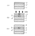
図1(a)〜(c)は、それぞれ本発明の光導波路の製造方法の実施の形態の一例を示す工程毎の断面図である。図1において、1は基板、2は光導波路のクラッド部となる下部クラッド層、3は光導波路のコア部およびクラッド部が形成される層であり、この層3は導波光よりも高エネルギーの光による光照射量の増加につれて屈折率が所定範囲内で小さくなる光学材料からなるものである。そして、4は層3中に形成されたコア部、5は層3に対してコア部4となる部分の領域の周囲に、コア部4よりも相対的に多くの照射量の導波光よりも高エネルギーの光を照射することによって、コア部4より屈折率を小さくして形成したクラッド部である。また、6は上部クラッド層であり、下部クラッド層2と層3に形成されたクラッド部5と上部クラッド層6とによりこの光導波路のクラッド部が構成されている。
【0020】
本発明の光導波路の製造方法においては、まず図1(a)に示すように、基板1上に下部クラッド層2を形成する。
【0021】
基板1には、光集積回路基板や光電子混在基板等の光信号を扱う基板として使用される種々の基板、例えばシリコン基板やアルミナ基板・ガラスセラミックス基板・多層セラミック基板・プラスチック電気配線基板・ポリイミド基板等が使用できる。
【0022】
基板1上に形成する下部クラッド層2は、例えば、導波光より高エネルギーの光の照射により屈折率が変化し、光照射量の増加につれて屈折率が所定範囲内で小さくなる光学材料からなる層を形成した後、後で形成するコア部4の屈折率よりもその屈折率が小さくなるような照射量の光を照射することにより形成する。
【0023】
または、コア部4よりも小さな屈折率を有するその他の光学材料からなる膜を形成しても良い。
【0024】
次に、同じく図1(a)に示すように、下部クラッド層2上に光導波路のコア部4およびクラッド部5を形成するための層3として、導波光よりも高エネルギーの光の照射により屈折率が変化し、光照射量の増加につれて屈折率が所定範囲内で小さくなる光学材料からなる層3を形成する。
【0025】
その後、図1(b)に示すように、例えばクラッド部5となる部分のみに所定光量の光を照射することにより、コア部4の屈折率よりもクラッド部5の屈折率が小さくなり、コア部4およびクラッド部5が形成される。
【0026】
ここで、クラッド部5となる部分のみに所定光量の光を照射するには、例えば、図1(b)に示すように周知のフォトリソグラフィで用いるようなフォトマスク7(遮光部に斜線を施して示す。)を介して、あるいは層3上に直接に金属薄膜による開口パターンを形成するなどしてコア部4となる部分を遮光した上で光を照射すればよい。また、レーザ光描画法により直接クラッド部5となる領域のみに光照射してもよい。その光照射量としては、光照射量の増加につれて屈折率が小さくなる光学材料に対して、光照射量と所定範囲内における屈折率変化量との関係を予め把握しておき、所望の光導波路を構成するためのコア部4およびクラッド部5の屈折率となるような光照射量を決定すればよい。
【0027】
なお、層3のコア部4となる領域の周囲に相対的に多量の光照射を行なってコア部4およびそれを内蔵するコア部4より屈折率が小さいクラッド部5を形成する場合、コア部4となる領域にも所望の屈折率となるような光量の光照射を行なうとともにその周囲のクラッド部5となる領域にはそれ以上の光量の光照射を行なう。
【0028】
次に、図1(c)に示すように、コア部4およびクラッド部5を形成した層の上面に上部クラッド層6を形成する。上部クラッド層6としては、コア部4よりも小さく、クラッド部5と同等の屈折率を有する膜を形成すればよい。例えば、フッ素樹脂・シロキサン系ポリマなどの樹脂系材料を用いれば、屈折率の制御が容易であり、スピンコート法などの簡便な方法で成膜でき、また、光透過性も優れており好適なものとなる。なお、上部クラッド層6は、必ず必要なものではなく、コア部4およびクラッド部5が大気あるいは真空に曝されていても良い。
【0029】
下部クラッド層2の屈折率や厚さ、コア部4の高さや幅や屈折率、上部クラッド層6の厚さや屈折率は、周知の光導波路に関する理論から検討・設計して設定すれば良い。
【0030】
本発明の光導波路を形成するための、導波光よりも高エネルギーの光の照射により屈折率が変化し、光照射量の増加につれて屈折率が所定範囲内で小さくなる光学材料としては、具体的には、そのような光の照射により膜材料の分解や重合あるいは色中心の生成等の膜材料の構造に変化が生じることにより、光照射量とともに屈折率が所定範囲内で小さくなるように変化する傾向を有する光学材料を用いれば良い。また、このような光学材料からなる膜を形成する方法としては、スピンコート法・ディップコート法・スプレーコート法・ローラーコート法・真空蒸着法等を用いれば良い。
【0031】
なお、本発明にかかる光学材料の屈折率を制御するための導波光よりも高エネルギーの光としては、導波光として一般的に近赤外光や赤外光が用いられることから、通常は可視光や紫外光を用いる。このように導波光よりも波長が短い高エネルギーの光を用いることにより、光学材料中において屈折率を変化させるのに必要な化学的な変化を生じさせることによって、光照射につれて所定範囲内で屈折率を小さくして、所望の屈折率で安定させて必要な屈折率を有するコア部および/またはクラッド部を形成することができる。
【0032】
また、かかる光学材料の屈折率を制御するための光は導波光よりも高エネルギーの光であることから、得られた光導波路のコア部に導波光を通して光信号を電波させるときには、その導波光によっては光学材料の屈折率は変化することはなく、光導波路として安定した屈折率を有し、良好な特性を有するものとして使用することができる。
【0033】
ここで、このような光照射量の増加につれて屈折率が小さくなる光学材料を用いる理由は、下部クラッド層2として光照射量の増加につれて屈折率が変化する光学材料からなる層を用いて、その層2の上に同じく光照射量の増加につれて屈折率が変化する光学材料からなる層3を形成して、それらに対する光照射量の差により屈折率差を生じさせてコア部4とクラッド部5とを形成しようとするとき、光照射量の増加につれて屈折率が大きくなる材料を用いた場合には、コア部4とクラッド部5とを形成するために照射した光が下部クラッド層2にも照射されて下部クラッド層2に対する光の照射量がコア部4の照射量よりも多くなるため、その結果として下部クラッド層2の屈折率がコア部4の屈折率よりも大きくなってしまうため、光導波路としての機能に障害をもたらすためである。
【0034】
これに対し、光照射量の増加につれて屈折率が小さくなる光学材料を用いることにより、下部クラッド層2への光の照射量がコア部4への光の照射量より多くなっても、下部クラッド層2の屈折率はコア部4の屈折率よりも小さいものとなるので、光導波路として適当なものとなる。
【0035】
次に、図2(a)〜(d)に、それぞれ本発明の光導波路の製造方法の実施の形態の他の例を示す工程毎の断面図を示す。
【0036】
図2において、11は基板、12は光導波路の下部クラッド層、13は光導波路のコア部14およびクラッド部15が形成される層であり、この層13は導波光よりも高エネルギーの光の照射によりシロキサン結合を形成することによって得られるシロキサン系ポリマからなる層である。また、この層13は、屈折率がそのような光の照射につれて所定範囲内で小さくなる光学材料でもある。14は層13中に形成されたコア部、15は層13に対してコア部14となる部分の領域の周囲に、コア部14よりも相対的に多くの照射量の光を照射することによって、屈折率をコア部14より小さくして形成したクラッド部である。また、16は上部クラッド層であり、下部クラッド層12と層13に形成されたクラッド部15と上部クラッド層16とによりこの光導波路のクラッド部が構成されている。
【0037】
このような本発明の光導波路の製造方法においても、まず図2(a)に示すように、基板11上に下部クラッド層12を形成する。
【0038】
基板11にも、基板1と同様に、光集積回路基板や光電子混在基板等の光信号を扱う基板として使用される種々の基板、例えばシリコン基板やアルミナ基板・ガラスセラミックス基板・多層セラミック基板・プラスチック電気配線基板・ポリイミド板等が使用できる。
【0039】
下部クラッド層12は、基板11上に、例えば導波光よりも高エネルギーの光の照射によりシロキサン結合を形成することによって得られるシロキサン系ポリマからなる層により形成し、これに対してコア部14の屈折率よりも下部クラッド層12の屈折率が小さくなるような、コア部14となる部分よりも多くの照射量の光照射を行なうことにより形成すればよい。または、コア部14よりも小さな屈折率を有するその他の光学材料からなる層を用いても良い。
【0040】
次に、図2(b)に示すように、下部クラッド層12上に、導波光よりも高エネルギーの光の照射によりシロキサン結合を形成することによって得られるシロキサン系ポリマからなる層13を形成する。このとき、この層13の全体にコア部14として適切な屈折率となるような所定光量の光照射を行なっておくとよい。
【0041】
その後、図2(c)に示すように、コア部14となる領域の周囲、すなわちクラッド部15となる部分のみに相対的に多量の光を照射することにより、コア部14の屈折率よりもクラッド部15の屈折率を所定範囲内で小さくして、コア部14およびクラッド部15を形成する。ここで、クラッド部15となる部分のみに所定光量の光を照射する方法としては、図2(c)に示すように、周知のフォトリソグラフィで用いるようなフォトマスク17(遮光部に斜線を施して示す。)を介して、あるいは層13上に直接に金属薄膜による開口パターンを形成するなどしてコア部14となる領域の部分を遮光した上で光を照射すればよい。また、レーザ光描画法により直接クラッド部15となる領域のみに光照射してもよい。
【0042】
次に、図2(d)に示すように、コア部14およびクラッド部15を形成した層の上面に上部クラッド層16を形成する。上部クラッド層16は、コア部14よりも小さな屈折率を有する光学材料からなる膜を形成すればよい。なお、上部クラッド層16は、必ず必要なものではなく、クラッド部15およびコア部14が大気あるいは真空に曝されていても良い。
【0043】
このような本発明の光導波路に用いる、導波光よりも高エネルギーの光の照射によりシロキサン結合を形成するシロキサン系ポリマからなる層は、シリコン(Si)原子にOH基と、メチル基等のアルキル基やフェニル基等の有機成分とが末端基として付帯したモノマーあるいはオリゴマーと、光反応型の重合促進剤と、有機溶媒とから成るシロキサン系ポリマ膜形成用溶液を基板上に塗布した後、光照射を行ない、脱水重合もしくは脱アルコール重合によりシロキサン結合を形成し、その後、加熱処理によって膜中に残留した溶媒や重合促進剤、または水やアルコール等の重合の際の副生成物等を膜外へ排出することによって得られた、シロキサン結合を主骨格とするシロキサン系ポリマ膜である。このような層13を形成する方法としては、スピンコート法・ディップコート法・スプレーコート法・ローラーコート法・真空蒸着法などを用いれば良い。
【0044】
本発明者は本発明に用いるシロキサン系ポリマについて鋭意検討・研究を重ねた結果、本シロキサン系ポリマからなる膜(層)の屈折率を、シロキサン結合を形成する際の光照射量を変えることにより精密に制御できることを見いだした。
【0045】
このような本シロキサン系ポリマの膜形成の際の光照射量と膜の屈折率との関係の例を、図3に線図で示す。
【0046】
図3において、横軸は膜形成の際の光照射量(単位:mJ/cm2 )であり、縦軸は得られたシロキサン系ポリマ膜の屈折率である。また、図中の黒点は測定結果を示している。ここで、照射した光には、導波光よりも高エネルギーの光として、重合促進剤に対して有効なエネルギー成分を有する高圧水銀ランプの紫外光を用いた。
【0047】
図3より分かるように、膜形成の際の光照射量を多くしていくと、光照射当初はシロキサン結合の形成が促進されて強固なシロキサン骨格が形成されるとともに、シロキサン系ポリマ膜の屈折率は所定の値まで一旦急激に増加する。そして、シロキサン系ポリマ膜の屈折率は材料の特性に応じてある光照射量で最大となり、その後、光照射量の増加につれて材料の特性に応じた所定の値を下限値として小さくなっていく。この理由は、以下のように考えられる。
【0048】
膜形成の際の光照射量を多くすると、シロキサン結合の形成が促進され強固なシロキサン骨格が形成されるとともに、シロキサン系ポリマ膜中に残留した溶媒や重合促進剤、また水やアルコールなどの重合の際の副生成物等が、光照射後の加熱処理によって膜外へ排出され易くなる。このとき、強固なシロキサン骨格の形状が保たれたまま、それがほとんど収縮することなく排出が行なわれるので、膜の密度が減少し、膜の屈折率が小さくなる。
【0049】
なお、このとき強固なシロキサン骨格の形状が保たれたままであり、この骨格が収縮することがないので、膜形成の際に膜厚の減少はなく、膜形成用溶液を塗布した際の表面の平坦性が膜形成後においてもそのまま保たれることとなり、下地基板に凹凸や表面粗さがあっても、優れた平坦化・平滑化が達成できる。
【0050】
このような層13に対するコア部14となる領域およびその周囲のクラッド部15となる領域への光照射量としては、層13に使用する光学材料について図3に示したような光照射量と屈折率変化量との所定範囲内における関係を予め把握しておき、所望の光導波路を得るためのコア部14およびクラッド部15の屈折率となるような光照射量を決定すればよい。
【0051】
ここで、コア部14への光照射量としては、光照射により十分なシロキサン結合が形成される、つまり、図3における屈折率が最大となる光照射量以上の光照射量とすることが望ましい。これは、十分な光照射によりコア部14中に十分なシロキサン結合が形成されることにより、コア部14が強固で安定なシロキサン系ポリマとなり、所望の屈折率を有するものとなるとともに、耐候性・熱安定性等が良くなるためである。
【0052】
一方、クラッド部15への光照射量としては、コア部14へ照射した光の光照射量よりも多い、より小さい屈折率となるような光照射量とする。これにより、クラッド部15の屈折率はコア部14の屈折率よりも小さくなり、光導波路として機能させることができるものとなる。
【0053】
このように、光照射量の増加につれて屈折率が小さくなる本シロキサン系ポリマを用いれば、下部クラッド層12に光照射によりシロキサン結合を形成することによって得られるシロキサン系ポリマを用いた場合でも、下部クラッド層12を形成した後に下部クラッド層12上にコア部14およびクラッド部15を形成する際の光照射が下部クラッド層12に及んでも、下部クラッド層12の屈折率を常にコア部14の屈折率よりも小さく保つことができ、光導波路として機能させることができるものとなる。また、コア部14およびクラッド部15となる層13を形成する前に、下部クラッド層12に光照射した後に加熱処理によって光重合促進材を揮発させあるいはその作用を無効化しておけば、下部クラッド層12上にコア部14およびクラッド部15を形成する際の光照射によっても下部クラッド層12の屈折率を変化させないようにすることができる。
【0054】
本発明の光導波路にかかる光照射によりシロキサン結合を形成することによって得られるシロキサン系ポリマを形成するのに用いるシロキサン系ポリマ膜形成用溶液に包含されるシリコン(Si)原子にOH基と、メチル基やフェニル基等の有機成分とが末端基として付帯したモノマーあるいはオリゴマーとしては、その種類が単一種でも複数種でも良い。また、その末端基のメチル基やフェニル基等の有機成分については、H原子がハロゲン化あるいは重水素化されていても良い。
【0055】
また、シロキサン系ポリマを用いることによる付随的な効果として、本発明のシロキサン系ポリマを用いた光導波路は、光照射によりシロキサン結合を形成することによって得られるこのシロキサン系ポリマを光導波路のコア部14およびクラッド部15に用いるものであることから、シロキサン結合を主骨格に持つことによる優れた耐熱性を有している。さらに、PMMA・ポリカーボネート・ポリイミド・BCB等のCH主成分のポリマに比べて含有CH基量が少ないので、CH基による赤外振動吸収が小さく、導波光として用いられる光が属する近赤外光域での光透過性が優れたものとなる。
【0056】
以上のように、本発明の光導波路の製造方法によれば、導波光よりも高エネルギーの光の照射により屈折率が変化する光学材料であって、光照射量の増加につれて屈折率が所定範囲内で小さくなる光学材料により光導波路のコア部およびクラッド部を形成しており、コア部よりも相対的に多くの照射量の光をクラッド部に照射することによってクラッド部の屈折率をコア部の屈折率よりも小さくしてコア部およびクラッド部を形成することから、コア部を形成する方法としてドライエッチングやウエットエッチング等を用いる必要がないので、ドライエッチングやウエットエッチング等を用いたコア部の加工に伴う煩雑な工程や加工形状の不備がなくなり、光導波路を簡便な方法で生産性が高く、しかも高い加工精度で製造することができる。
【0057】
【実施例】
次に、本発明の光導波路の製造方法について具体例を説明する。
【0058】
〔例1〕
まず、シリコンからなる基板上に、シリコン原子にOH基とメチル基およびフェニル基とが末端基として付帯したモノマーと、光反応型の重合促進剤と、有機溶媒とから成るシロキサン系ポリマ膜形成用溶液をスピンコート法により塗布し、100 ℃/30分間の加熱処理を行ない、有機溶媒を蒸発させた。その後、高圧水銀ランプの紫外光を基板全面に1500mJ/cm2 の光照射量で照射して、150 ℃/60分間の加熱処理を行ない、膜厚15μm・屈折率1.4367のシロキサン系ポリマ膜からなる下部クラッド層を形成した。
【0059】
次に、この下部クラッド層上に、下部クラッド層を形成した際に用いたシロキサン系ポリマ膜形成用溶液をスピンコート法により塗布し、100 ℃/30分間の加熱処理を行ない、有機溶媒を蒸発させて、コア部およびクラッド部を形成するためのシロキサン系ポリマ膜からなる層を形成した。その層の厚さは5μmとした。その後、高圧水銀ランプの紫外光を基板全面に100 mJ/cm2 の光照射量で照射した。
【0060】
さらに、幅1μmから50μmの種々の幅のストライプ状の遮光部分を有するフォトマスクにより、コア部となる領域の部分を遮光して、その周囲のクラッド部となる部分に高圧水銀ランプの紫外光を1500mJ/cm2 の光照射量で照射した。
【0061】
以上により、屈折率が1.4367で厚さが15μmの下部クラッド層上に、屈折率が1.440 で種々の幅を持ち、高さが5μmのコア部と、屈折率が1.4367でコア部と同じ層に形成されたクラッド部を有し、上部クラッド層を空気層とした光導波路を作製した。
【0062】
この光導波路について、波長1.3 μmのレーザ光を入射させ伝搬させて出射光を赤外線カメラで観察したところ、幅10μm以下の遮光幅で作製した光導波路がシングルモードとなっていることを確認した。また、出射光強度を光パワーメータで測定することにより伝搬損失を評価したところ、0.2 dB/cm程度の損失であり、光導波路として十分な性能であることを確認した。
【0063】
〔例2〕
まず、シリコンからなる基板上に、シリコン原子にOH基とメチル基およびフェニル基とが末端基として付帯したモノマーと、光反応型の重合促進剤と、有機溶媒とから成るシロキサン系ポリマ膜形成用溶液をスピンコート法により塗布し、100 ℃/30分間の加熱処理を行ない、有機溶媒を蒸発させた。その後、高圧水銀ランプの紫外光を基板全面に1500mJ/cm2 の光照射量で照射して、150 ℃/60分間の加熱処理を行ない、膜厚15μm・屈折率1.4367のシロキサン系ポリマ膜からなる下部クラッド層を形成した。
【0064】
次に、この下部クラッド層上に、下部クラッド層を形成した際に用いたシロキサン系ポリマ膜形成用溶液をスピンコート法により塗布し、100 ℃/30分間の加熱処理を行ない、有機溶媒を蒸発させて、コア部およびクラッド部を形成するためのシロキサン系ポリマ膜からなる層を形成した。その層の厚さは8μmとした。その後、高圧水銀ランプの紫外光を基板全面に100 mJ/cm2 の光照射量で照射した。
【0065】
さらに、幅1μmから50μmの種々の幅のストライプ状の遮光部分を有するフォトマスクにより、コア部となる領域の部分を遮光して、その周囲のクラッド部となる部分に高圧水銀ランプの紫外光を1500mJ/cm2 の光照射量で照射し、150 ℃/60分間の加熱処理を行なった。
【0066】
次に、コア部およびクラッド部を形成した層の上に、下部クラッド層を形成した際に用いたシロキサン系ポリマ膜形成用溶液をスピンコート法により塗布し、100 ℃/30分間および150 ℃/60分間の加熱処理を行なって、光を未照射として、シロキサン系ポリマ膜からなる屈折率が1.4360で厚さが15μmの上部クラッド層を形成した。
【0067】
以上により、屈折率が1.4367で厚さが15μmの下部クラッド層上に、屈折率が1.440 で種々の幅を持ち、高さが8μmのコア部と、屈折率が1.4367でコア部と同じ層に形成されたクラッド部とを有し、上部クラッド層が屈折率が1.4360で厚さが15μmの光が未照射のシロキサン系ポリマ膜からなる光導波路を作製した。
【0068】
この光導波路について、波長1.3 μmのレーザ光を入射させ伝搬させて出射光を赤外線カメラで観察したところ、幅10μm以下の遮光幅で作製した光導波路がシングルモードとなっていることを確認した。また、出射光強度を光パワーメータで測定することにより伝搬損失を評価したところ、0.4 dB/cm程度の損失であり、光導波路として十分な性能であることを確認した。
【0069】
〔例3〕
まず、シリコンからなる基板上に、シリコン原子にOH基とメチル基およびフェニル基とが末端基として付帯したモノマーと、光反応型の重合促進剤と、有機溶媒とから成るシロキサン系ポリマ膜形成用溶液をスピンコート法により塗布し、100 ℃/30分間の加熱処理を行ない、有機溶媒を蒸発させた。その後、高圧水銀ランプの紫外光を基板全面に1500mJ/cm2 の光照射量で照射して、150 ℃/60分間の加熱処理を行ない、膜厚15μm・屈折率1.4367のシロキサン系ポリマ膜からなる下部クラッド層を形成した。
【0070】
次に、この下部クラッド層上に、下部クラッド層を形成した際に用いたシロキサン系ポリマ膜形成用溶液をスピンコート法により塗布し、100 ℃/30分間の加熱処理を行ない、有機溶媒を蒸発させて、コア部およびクラッド部を形成するためのシロキサン系ポリマ膜からなる層を形成した。その層の厚さは6μmとした。その後、高圧水銀ランプの紫外光を基板全面に100 mJ/cm2 の光照射量で照射した。
【0071】
さらに、幅1μmから50μmの種々の幅のストライプ状の遮光部分を有するフォトマスクにより、コア部となる領域の部分を遮光して、その周囲のクラッド部となる部分に高圧水銀ランプの紫外光を1500mJ/cm2 の光照射量で照射し、150 ℃/60分間の加熱処理を行なった。
【0072】
次に、コア部およびクラッド部を形成した層の上に、環化ポリフッ化エチレン樹脂をフッ素系有機溶媒に溶解した溶液をスピンコート法により塗布し、150 ℃/60分間の加熱処理を行ない、有機溶媒を蒸発させて、屈折率が1.330 で厚さが15μmの上部クラッド層を形成した。
【0073】
以上により、屈折率が1.4367で厚さが15μmの下部クラッド層上に、屈折率が1.440 で種々の幅を持ち、高さが6μmのコア部と、屈折率が1.4367でコア部と同じ層に形成されたクラッド部とを有し、上部クラッド層が屈折率が1.330 で厚さが15μmの環化ポリフッ化エチレン樹脂からなる光導波路を作製した。
【0074】
この光導波路について、波長1.3 μmのレーザ光を入射させ伝搬させて出射光を赤外線カメラで観察したところ、幅10μm以下の遮光幅で作製した光導波路がシングルモードとなっていることを確認した。また、出射光強度を光パワーメータで測定することにより伝搬損失を評価したところ、0.2 dB/cm程度の損失であり、光導波路として十分な性能であることを確認した。
【0075】
以上のように、本発明によれば、簡便な方法で高い生産性で、しかも高い加工精度で、良好な特性の有機系光導波路を作製できることが確認できた。
【0076】
なお、本発明は以上の実施の形態の例に限定されるものではなく、本発明の要旨を逸脱しない範囲で種々の変更・改良を加えることは何ら差し支えない。例えば、コア部およびそれを内蔵するクラッド部を形成するための光学材料としては、屈折率を制御する光として紫外光や可視光だけではなくX線を用いて屈折率が制御できる光学材料であってもよい。
【0079】
【発明の効果】
本発明の光導波路の製造方法は、シロキサン系ポリマからなる、コア部およびクラッド部を備えた光導波路の製造方法であって、
基板上に、シリコン原子にOH基と、アルキル基やフェニル基等の有機成分とが末端基として付帯したモノマーあるいはオリゴマーと、光反応型の重合促進剤と、有機溶媒と、から成るシロキサン系ポリマ膜形成用溶液の塗布層を形成する工程と、
前記塗布層の前記コア部となる領域に導波光よりも高エネルギーの光の照射によりシロキサン結合を形成させるとともに、シロキサン系ポリマ膜の屈折率が最大となる光照射量以上の照射を行なって、いったん屈折率を上昇させた後に減少させ、前記コア部となる前記領域の周囲に相対的に多量の光の照射を行なって、前記コア部およびそれを内蔵するこのコア部より屈折率を小さくしたクラッド部を形成する工程とを具備することから、コア部の形成に際してドライエッチングやウエットエッチングなどを用いる必要がないため、ドライエッチングやウエットエッチング等を用いたコア部の加工に伴う煩雑な工程をなくすことができ、加工形状の不備等をなくすことができて、生産性が高く、しかも高い加工精度で光導波路を製造することができる。また、複数の光導波路を上下に積層形成する場合であってもそれぞれの光導波路の表面に凹凸が生じることはないので、そのような凹凸による悪影響の問題をなくすことができる。
【0080】
以上のように、本発明によれば、簡便な方法で生産性が高く、しかも高い加工精度で製造できる光導波路および光導波路の製造方法を提供することができた。
【図面の簡単な説明】
【図1】(a)〜(c)は、それぞれ本発明の光導波路の製造方法の実施の形態の一例を示す工程毎の断面図である。
【図2】(a)〜(d)は、それぞれ本発明の光導波路の製造方法の実施の形態の他の例を示す工程毎の断面図である。
【図3】本発明の光導波路に用いる光学材料としてのシロキサン系ポリマ膜の膜形成の際の光照射量と屈折率との関係を示す線図である。
【符合の説明】
1、11・・・基板
2、12・・・下部クラッド層
3、13・・・コア部およびクラッド部を形成するための層
4、14・・・光導波路のコア部
5、15・・・光導波路のクラッド部
6、16・・・上部クラッド層[0001]
BACKGROUND OF THE INVENTION
The present invention relates to an optical waveguide used in an optical communication module or the like.RoadMore specifically, the manufacturing method relates to a three-dimensional waveguide-shaped optical waveguide that can be manufactured by controlling the refractive index by light irradiation.RoadIt relates to a manufacturing method.
[0002]
[Prior art]
Conventionally, as an optical waveguide used for transmitting an optical signal in an optical communication module or the like, for example, a three-dimensional waveguide-shaped clad portion made of a silica film formed by a flame deposition method on a quartz glass substrate or a silicon substrate, and There have been silica-based optical waveguides in which a core part is formed, optical waveguides in which a lithium niobate single crystal substrate is used as a cladding part, and Ti is thermally diffused on the substrate to form a core part in a three-dimensional waveguide shape.
[0003]
However, since these conventional optical waveguides require heat treatment at a high temperature of 1000 ° C. or higher in the production process, it is difficult to produce desired optical waveguides on various substrates. Therefore, from the viewpoint of easy fabrication of optical waveguides, it is considered to use organic optical waveguides made of organic optical materials that can be formed at low temperatures instead of these conventional optical waveguides that require high-temperature processing during fabrication. Has been. For example, PMMA (polymethylmethacrylate), polycarbonate, polyimide, polysiloxane, BCB (benzocyclobutene) and the like have been studied as organic optical materials used for the organic optical waveguide.
[0004]
As a method of manufacturing an optical waveguide made of such an organic optical material, usually, a lower clad layer is formed on a silicon substrate or a glass substrate, and then a core layer having a higher refractive index than the lower clad layer is formed. Next, the core layer is processed by dry etching such as RIE (reactive ion etching) or wet etching using a solvent by using a thin film microfabrication technique, and then the refractive index is lower than that of the core. An optical waveguide having a three-dimensional waveguide shape in which a core portion is built in a clad portion is formed by covering an upper clad layer having a refractive index.
[0005]
In JP-A-6-172533, in a method for producing a polysiloxane-based optical waveguide, including a step of forming a lower clad layer on a substrate, a step of forming a core portion, and a step of forming an upper clad. It has been proposed to form the core part by a process of insolubilizing the polymer by irradiation with deep ultraviolet rays or an electron beam and a process of removing the unnecessary part.
[0006]
[Problems to be solved by the invention]
However, when dry etching is used in the formation of the core part when manufacturing an optical waveguide, a complicated and sophisticated process and control are required for the mask pattern manufacturing process and dry etching itself during dry etching. There is a problem that a desired optical waveguide cannot be easily obtained. Further, since various processes take time and the etching rate of dry etching itself is small, there is a problem that it takes a long time to manufacture an optical waveguide.
[0007]
On the other hand, when wet etching using a solvent is used, it is difficult to precisely control the processing shape of the core because isotropic etching proceeds, and an optical waveguide that requires submicron processing accuracy is required. And the production of a functional optical circuit using such an optical waveguide is difficult.
[0008]
On the other hand, when a polymer insolubilization process and an unnecessary part removal process by irradiation with deep ultraviolet rays or an electron beam as proposed in JP-A-6-172533 are used, a solvent is used. Compared with the case of using the wet etching, the processing shape of the core portion can be controlled more precisely, and the process becomes simpler than the case of using the dry etching. However, there is a problem that the process of removing the unnecessary part is necessary and the process is still complicated, and the wall surface of the core part is roughened at the time of removing the unnecessary part, causing light scattering loss. there were.
[0009]
In addition, when the clad part is coated after the convex core part is formed, irregularities are generated on the surface of the clad part. Therefore, when the optical waveguides are stacked up and down, the optical waveguide formed in a later step The processing accuracy when forming the core part of the optical waveguide deteriorates due to the unevenness of the optical waveguide formed earlier, or light is lost due to the influence of the unevenness when light is propagated to the optical waveguide formed in the later process There was a problem that occurred.
[0010]
The present invention has been devised in view of the above-mentioned problems of the prior art, and its object is to achieve high productivity with a simple method and high manufacturing accuracy.LightAn object of the present invention is to provide a method for manufacturing a waveguide.
[0013]
[Means for Solving the Problems]
The method for producing an optical waveguide of the present invention includes:A method for producing an optical waveguide comprising a core part and a clad part, comprising a siloxane polymer,
On the boardFor forming a siloxane polymer film comprising a monomer or oligomer having an OH group and an organic component such as an alkyl group or phenyl group attached to a silicon atom as a terminal group, a photoreactive polymerization accelerator, and an organic solvent Forming a coating layer of the solution;
In the region to be the core part of the coating layerFormation of siloxane bonds by irradiation with light of higher energy than guided lightAs well as,Irradiate more than the light dose that maximizes the refractive index of the siloxane polymer film, and then increase the refractive index and decrease it to become the core part.A relatively large amount around the areaLight ofAnd a step of forming a clad portion having a refractive index smaller than that of the core portion including the core portion and the core portion including the core portion.
[0016]
Therefore, even when a plurality of optical waveguides are stacked on top and bottom, the surface of each optical waveguide is not uneven, and the processing accuracy of the optical waveguide formed in the subsequent process is formed in the previous process. Further, there is no problem that the optical waveguide is deteriorated due to the unevenness of the optical waveguide, or light is lost due to the unevenness when the light is propagated to the optical waveguide formed in a later process.
[0017]
Further, the method for producing an optical waveguide of the present invention includesA method for producing an optical waveguide comprising a core part and a clad part, comprising a siloxane polymer,
A siloxane polymer comprising a monomer or oligomer having an OH group and an organic component such as an alkyl group or phenyl group attached to a silicon atom as a terminal group, a photoreactive polymerization accelerator, and an organic solvent on a substrate. Forming a coating layer of the film-forming solution;
Using this layer for the core and cladding of the optical waveguide,In the area that becomes the core of the coating layerFormation of siloxane bonds by irradiation with light of higher energy than guided lightAs well as,Irradiate more than the light dose that maximizes the refractive index of the siloxane polymer film, and then increase the refractive index and decrease it to become the core partBy irradiating the periphery of the region, that is, the region that becomes the clad portion, with a relatively larger amount of light than the region that becomes the core portion,Core part and built-in itThe refractive index was made smaller than this coreForming a clad portion. As a result, it is not necessary to use dry etching or wet etching when forming the core portion, so that complicated processes associated with processing of the core portion using dry etching, wet etching, etc. can be eliminated, and the processing shape is incomplete. The optical waveguide can be manufactured with high productivity and high processing accuracy.
[0018]
DETAILED DESCRIPTION OF THE INVENTION
Hereinafter, the optical waveguide of the present invention.RoadA manufacturing method will be described with reference to the drawings.
[0019]
1A to 1C are cross-sectional views for each process showing an example of an embodiment of a method for manufacturing an optical waveguide according to the present invention.is there. In FIG. 1, 1 is a substrate, 2 is a lower clad layer that becomes a clad portion of an optical waveguide, 3 is a layer in which a core portion and a clad portion of the optical waveguide are formed, and this
[0020]
In the method of manufacturing an optical waveguide according to the present invention, first, a
[0021]
The substrate 1 includes various substrates used as optical signal processing substrates such as optical integrated circuit substrates and optoelectronic mixed substrates, such as silicon substrates, alumina substrates, glass ceramic substrates, multilayer ceramic substrates, plastic electrical wiring substrates, and polyimide substrates. Etc. can be used.
[0022]
The lower
[0023]
Alternatively, a film made of another optical material having a refractive index smaller than that of the
[0024]
Next, as shown in FIG. 1A, the
[0025]
Thereafter, as shown in FIG. 1 (b), for example, by irradiating only a portion that becomes the
[0026]
Here, in order to irradiate only a portion that becomes the
[0027]
When a relatively large amount of light is irradiated around the area of the
[0028]
Next, as shown in FIG. 1C, an upper
[0029]
The refractive index and thickness of the
[0030]
As an optical material for forming the optical waveguide of the present invention, the refractive index is changed by irradiation with light having a higher energy than the guided light, and the refractive index decreases within a predetermined range as the amount of light irradiation increases. Changes in the refractive index within the specified range with the amount of light irradiation due to changes in the structure of the film material such as decomposition of the film material, polymerization or generation of color centers. An optical material having a tendency to be used may be used. As a method for forming a film made of such an optical material, a spin coating method, a dip coating method, a spray coating method, a roller coating method, a vacuum deposition method, or the like may be used.
[0031]
Note that light having higher energy than the guided light for controlling the refractive index of the optical material according to the present invention is generally visible because near infrared light or infrared light is generally used as the guided light. Light or ultraviolet light is used. By using high energy light having a wavelength shorter than that of the guided light in this way, a chemical change necessary for changing the refractive index in the optical material is generated, so that the light is refracted within a predetermined range as the light is irradiated. The core part and / or the clad part having the required refractive index can be formed by reducing the refractive index and stabilizing the desired refractive index.
[0032]
In addition, since the light for controlling the refractive index of the optical material is light having higher energy than the guided light, when the optical signal is transmitted through the guided light to the core portion of the obtained optical waveguide, the guided light is used. In some cases, the refractive index of the optical material does not change, and it can be used as an optical waveguide having a stable refractive index and good characteristics.
[0033]
Here, the reason for using an optical material whose refractive index decreases as the amount of light irradiation increases is that the
[0034]
On the other hand, by using an optical material whose refractive index decreases as the light irradiation amount increases, even if the light irradiation amount to the
[0035]
Next, FIGS. 2A to 2D are cross-sectional views for each process showing another example of the embodiment of the optical waveguide manufacturing method of the present invention.ShowThe
[0036]
In FIG. 2, 11 is a substrate, 12 is a lower clad layer of the optical waveguide, 13 is a layer in which the
[0037]
Also in such an optical waveguide manufacturing method of the present invention, first, a lower
[0038]
Similarly to the substrate 1, the
[0039]
The
[0040]
Next, as shown in FIG. 2B, a
[0041]
Thereafter, as shown in FIG. 2 (c), a relatively large amount of light is irradiated to the periphery of the region that becomes the
[0042]
Next, as shown in FIG. 2D, the upper clad
[0043]
A layer made of a siloxane-based polymer that forms a siloxane bond by irradiation with light having a higher energy than that of the guided light used in the optical waveguide of the present invention is composed of silicon (Si) atoms with OH groups and alkyl groups such as methyl groups. A siloxane polymer film-forming solution comprising a monomer or an oligomer attached with an organic component such as a group or a phenyl group as a terminal group, a photoreactive polymerization accelerator, and an organic solvent is applied onto a substrate, and then light is applied. Irradiate to form a siloxane bond by dehydration polymerization or dealcoholization polymerization, and then remove the solvent and polymerization accelerator remaining in the film by heat treatment, or by-products during polymerization of water, alcohol, etc. It is a siloxane-based polymer film having a siloxane bond as the main skeleton obtained by discharging into As a method for forming such a
[0044]
As a result of intensive investigation and research on the siloxane polymer used in the present invention, the present inventor has changed the refractive index of the film (layer) made of the siloxane polymer by changing the amount of light irradiation when forming the siloxane bond. I found that I could control it precisely.
[0045]
An example of the relationship between the amount of light irradiation and the refractive index of the film during the film formation of the siloxane polymer is shown in FIG.
[0046]
In FIG. 3, the horizontal axis represents the amount of light irradiation during film formation (unit: mJ / cm).2The vertical axis represents the refractive index of the obtained siloxane polymer film. Moreover, the black dots in the figure indicate the measurement results. Here, the ultraviolet light of the high pressure mercury lamp which has an energy component effective with respect to a polymerization accelerator was used for the irradiated light as light with higher energy than waveguide light.
[0047]
As can be seen from FIG. 3, when the amount of light irradiation during film formation is increased, formation of a siloxane bond is promoted at the beginning of light irradiation to form a strong siloxane skeleton, and the refraction of the siloxane polymer film The rate once increases rapidly to a predetermined value. The refractive index of the siloxane-based polymer film becomes maximum at a certain light irradiation amount according to the material properties, and thereafter, as the light irradiation amount increases, a predetermined value according to the material properties becomes a lower limit value. The reason is considered as follows.
[0048]
When the amount of light irradiation during film formation is increased, formation of siloxane bonds is promoted and a strong siloxane skeleton is formed. In addition, a solvent or polymerization accelerator remaining in the siloxane polymer film, or polymerization such as water or alcohol By-products and the like at this time are easily discharged out of the film by the heat treatment after light irradiation. At this time, since the strong siloxane skeleton is maintained and the discharge is carried out with almost no contraction, the density of the film is reduced and the refractive index of the film is reduced.
[0049]
At this time, the shape of the strong siloxane skeleton remains maintained, and the skeleton does not shrink. Therefore, there is no reduction in the film thickness during film formation, and the surface of the film upon application of the film forming solution is not affected. Flatness is maintained as it is even after the film is formed, and even if the base substrate has irregularities and surface roughness, excellent flattening and smoothing can be achieved.
[0050]
As for the amount of light irradiation to the region that becomes the
[0051]
Here, it is desirable that the light irradiation amount to the
[0052]
On the other hand, the light irradiation amount to the
[0053]
As described above, when the siloxane polymer having a refractive index that decreases as the light irradiation amount increases, the lower
[0054]
The silicon (Si) atoms included in the solution for forming a siloxane-based polymer film used to form a siloxane-based polymer obtained by forming a siloxane bond by light irradiation applied to the optical waveguide of the present invention, an OH group, and methyl As the monomer or oligomer attached with an organic component such as a group or a phenyl group as a terminal group, the type may be a single type or a plurality of types. Moreover, about organic components, such as the methyl group of a terminal group, and a phenyl group, H atom may be halogenated or deuterated.
[0055]
Further, as an incidental effect of using the siloxane polymer, the optical waveguide using the siloxane polymer of the present invention is obtained by forming the siloxane polymer obtained by forming a siloxane bond by light irradiation with the core portion of the optical waveguide. Since it is used for 14 and the clad
[0056]
As described above, the optical waveguide of the present invention.RoadAccording to the manufacturing method, an optical material whose refractive index is changed by irradiation with light having a higher energy than that of guided light, and the refractive index of the optical waveguide is reduced within a predetermined range as the amount of light irradiation increases. And the clad part is irradiated with light of a relatively larger amount of irradiation than the core part, so that the refractive index of the clad part is made smaller than the refractive index of the core part. Since the clad portion is formed, it is not necessary to use dry etching or wet etching as a method of forming the core portion. Therefore, complicated processes and processing shapes associated with processing of the core portion using dry etching, wet etching, etc. There are no deficiencies, and the optical waveguide can be manufactured with a simple method with high productivity and high processing accuracy.
[0057]
【Example】
Next, the optical waveguide of the present inventionRoadA specific example of the manufacturing method will be described.
[0058]
[Example 1]
First, on a substrate made of silicon, for forming a siloxane polymer film comprising a monomer in which an OH group, a methyl group, and a phenyl group are attached to silicon atoms as terminal groups, a photoreactive polymerization accelerator, and an organic solvent. The solution was applied by a spin coating method and subjected to a heat treatment at 100 ° C./30 minutes to evaporate the organic solvent. Then, UV light from a high-pressure mercury lamp is applied to the entire surface of the substrate at 1500 mJ / cm.2A lower cladding layer made of a siloxane polymer film having a film thickness of 15 μm and a refractive index of 1.4367 was formed by performing irradiation at 150 ° C. for 60 minutes.
[0059]
Next, on this lower clad layer, the siloxane polymer film forming solution used when forming the lower clad layer is applied by spin coating, and heat treatment is performed at 100 ° C./30 minutes to evaporate the organic solvent. Thus, a layer made of a siloxane polymer film for forming the core part and the clad part was formed. The thickness of the layer was 5 μm. After that, UV light from a high-pressure mercury lamp is applied to the entire surface of the substrate at 100 mJ / cm.2Irradiation was performed at a light irradiation amount of.
[0060]
Furthermore, the photomask having stripe-shaped light-shielding portions with various widths of 1 μm to 50 μm is used to shield the portion of the region that becomes the core portion, and the ultraviolet light of the high-pressure mercury lamp to the portion that becomes the surrounding cladding portion 1500mJ / cm2Irradiation was performed at a light irradiation amount of.
[0061]
As described above, on the lower clad layer having a refractive index of 1.4367 and a thickness of 15 μm, a core portion having a refractive index of 1.440 and various widths and a height of 5 μm, and a refractive index of 1.4367 having the same layer as the core portion. An optical waveguide having the formed clad part and having the upper clad layer as an air layer was produced.
[0062]
With respect to this optical waveguide, laser light having a wavelength of 1.3 μm was incident and propagated, and the emitted light was observed with an infrared camera. As a result, it was confirmed that the optical waveguide produced with a light-shielding width of 10 μm or less was single mode. Further, when the propagation loss was evaluated by measuring the intensity of the emitted light with an optical power meter, it was confirmed that the loss was about 0.2 dB / cm, which was sufficient as an optical waveguide.
[0063]
[Example 2]
First, on a substrate made of silicon, for forming a siloxane polymer film comprising a monomer in which an OH group, a methyl group, and a phenyl group are attached to silicon atoms as terminal groups, a photoreactive polymerization accelerator, and an organic solvent. The solution was applied by a spin coating method and subjected to a heat treatment at 100 ° C./30 minutes to evaporate the organic solvent. Then, UV light from a high-pressure mercury lamp is applied to the entire surface of the substrate at 1500 mJ / cm.2A lower cladding layer made of a siloxane polymer film having a film thickness of 15 μm and a refractive index of 1.4367 was formed by performing irradiation at 150 ° C. for 60 minutes.
[0064]
Next, on this lower clad layer, the siloxane polymer film forming solution used when forming the lower clad layer is applied by spin coating, and heat treatment is performed at 100 ° C./30 minutes to evaporate the organic solvent. Thus, a layer made of a siloxane polymer film for forming the core part and the clad part was formed. The thickness of the layer was 8 μm. After that, UV light from a high-pressure mercury lamp is applied to the entire surface of the substrate at 100 mJ / cm.2Irradiation was performed at a light irradiation amount of.
[0065]
Furthermore, the photomask having stripe-shaped light-shielding portions with various widths of 1 μm to 50 μm is used to shield the portion of the region that becomes the core portion, and the ultraviolet light of the high-pressure mercury lamp to the portion that becomes the surrounding cladding portion 1500mJ / cm2Was irradiated at a light irradiation amount of 150 ° C. for 60 minutes.
[0066]
Next, a solution for forming a siloxane-based polymer film used when forming the lower cladding layer is applied onto the layer on which the core portion and the cladding portion have been formed by spin coating, and the coating is performed at 100 ° C./30 minutes and 150 ° C. / A heat treatment for 60 minutes was performed to form an upper cladding layer made of a siloxane polymer film having a refractive index of 1.4360 and a thickness of 15 μm without being irradiated with light.
[0067]
As described above, a core part having a refractive index of 1.4367 and a thickness of 15 μm, a refractive index of 1.440 and various widths and a height of 8 μm, and a refractive index of 1.4367 having the same layer as the core part. An optical waveguide made of a siloxane-based polymer film having a clad portion formed, an upper clad layer having a refractive index of 1.4360 and a thickness of 15 μm and not irradiated with light was produced.
[0068]
With respect to this optical waveguide, laser light having a wavelength of 1.3 μm was incident and propagated, and the emitted light was observed with an infrared camera. As a result, it was confirmed that the optical waveguide produced with a light-shielding width of 10 μm or less was single mode. Further, when the propagation loss was evaluated by measuring the emitted light intensity with an optical power meter, it was confirmed that the loss was about 0.4 dB / cm, which was sufficient as an optical waveguide.
[0069]
[Example 3]
First, on a substrate made of silicon, for forming a siloxane polymer film comprising a monomer in which an OH group, a methyl group, and a phenyl group are attached to silicon atoms as terminal groups, a photoreactive polymerization accelerator, and an organic solvent. The solution was applied by a spin coating method and subjected to a heat treatment at 100 ° C./30 minutes to evaporate the organic solvent. Then, UV light from a high-pressure mercury lamp is applied to the entire surface of the substrate at 1500 mJ / cm.2A lower cladding layer made of a siloxane polymer film having a film thickness of 15 μm and a refractive index of 1.4367 was formed by performing irradiation at 150 ° C. for 60 minutes.
[0070]
Next, on this lower clad layer, the siloxane polymer film forming solution used when forming the lower clad layer is applied by spin coating, and heat treatment is performed at 100 ° C./30 minutes to evaporate the organic solvent. Thus, a layer made of a siloxane polymer film for forming the core part and the clad part was formed. The thickness of the layer was 6 μm. After that, UV light from a high-pressure mercury lamp is applied to the entire surface of the substrate at 100 mJ / cm.2Irradiation was performed at a light irradiation amount of.
[0071]
Furthermore, the photomask having stripe-shaped light-shielding portions with various widths of 1 μm to 50 μm is used to shield the portion of the region that becomes the core portion, and the ultraviolet light of the high-pressure mercury lamp to the portion that becomes the surrounding cladding portion 1500mJ / cm2Was irradiated at a light irradiation amount of 150 ° C. for 60 minutes.
[0072]
Next, a solution obtained by dissolving a cyclized polyfluorinated ethylene resin in a fluorine-based organic solvent is applied onto the layer in which the core part and the clad part are formed by a spin coating method, and a heat treatment at 150 ° C./60 minutes is performed. The organic solvent was evaporated to form an upper cladding layer having a refractive index of 1.330 and a thickness of 15 μm.
[0073]
As described above, on the lower clad layer having a refractive index of 1.4367 and a thickness of 15 μm, a core portion having a refractive index of 1.440 and various widths and a height of 6 μm, and a refractive index of 1.4367 having the same layer as the core portion. An optical waveguide made of a cyclized polyfluorinated ethylene resin having a clad portion formed and an upper clad layer having a refractive index of 1.330 and a thickness of 15 μm was produced.
[0074]
With respect to this optical waveguide, laser light having a wavelength of 1.3 μm was incident and propagated, and the emitted light was observed with an infrared camera. As a result, it was confirmed that the optical waveguide produced with a light-shielding width of 10 μm or less was single mode. Further, when the propagation loss was evaluated by measuring the intensity of the emitted light with an optical power meter, it was confirmed that the loss was about 0.2 dB / cm, which was sufficient as an optical waveguide.
[0075]
As described above, according to the present invention, it was confirmed that an organic optical waveguide having good characteristics can be produced with high productivity and high processing accuracy by a simple method.
[0076]
It should be noted that the present invention is not limited to the examples of the embodiments described above, and various modifications and improvements can be added without departing from the scope of the present invention. For example, an optical material for forming a core portion and a clad portion including the core portion is an optical material whose refractive index can be controlled using X-rays as well as ultraviolet light and visible light as light for controlling the refractive index. May be.
[0079]
【The invention's effect】
BookThe optical waveguide manufacturing method of the invention isA method for producing an optical waveguide comprising a core part and a clad part, comprising a siloxane polymer,
On the boardFor forming a siloxane polymer film comprising a monomer or oligomer having an OH group and an organic component such as an alkyl group or phenyl group attached to a silicon atom as a terminal group, a photoreactive polymerization accelerator, and an organic solvent Forming a coating layer of the solution;
In the region to be the core part of the coating layerFormation of siloxane bonds by irradiation with light of higher energy than guided lightAs well as,Irradiate more than the light dose that maximizes the refractive index of the siloxane polymer film, and then increase the refractive index and decrease it to become the core part.A relatively large amount around the areaLight ofTo form the core part and a clad part having a refractive index smaller than that of the core part in which the core part is incorporated. Therefore, it is necessary to use dry etching or wet etching for forming the core part. Therefore, it is possible to eliminate complicated processes associated with core processing using dry etching, wet etching, etc., eliminate defects in the processing shape, etc., and achieve high productivity and high processing accuracy. An optical waveguide can be manufactured.Further, even when a plurality of optical waveguides are stacked on top and bottom, irregularities do not occur on the surfaces of the respective optical waveguides, so the problem of adverse effects due to such irregularities can be eliminated.
[0080]
As described above, according to the present invention, it is possible to provide an optical waveguide that can be manufactured with high productivity and high processing accuracy by a simple method, and an optical waveguide manufacturing method.
[Brief description of the drawings]
FIGS. 1A to 1C are cross-sectional views for each process showing an example of an embodiment of an optical waveguide manufacturing method according to the present invention.is there.
FIGS. 2A to 2D are cross-sectional views for each process showing another example of the embodiment of the optical waveguide manufacturing method of the present invention.is there.
FIG. 3 is a diagram showing a relationship between a light irradiation amount and a refractive index when forming a siloxane polymer film as an optical material used in the optical waveguide of the present invention.
[Explanation of sign]
1, 11 ... substrate
2, 12 ... Lower cladding layer
3, 13 ... Layers for forming the core and cladding
4, 14 ... Optical waveguide core
5, 15 ... Clad part of optical waveguide
6, 16 ... upper clad layer
Claims (1)
基板上に、シリコン原子にOH基と、アルキル基やフェニル基等の有機成分とが末端基として付帯したモノマーあるいはオリゴマーと、光反応型の重合促進剤と、有機溶媒と、から成るシロキサン系ポリマ膜形成用溶液の塗布層を形成する工程と、
前記塗布層の前記コア部となる領域に導波光よりも高エネルギーの光の照射によりシロキサン結合を形成させるとともに、シロキサン系ポリマ膜の屈折率が最大となる光照射量以上の照射を行なって、いったん屈折率を上昇させた後に減少させ、前記コア部となる前記領域の周囲に相対的に多量の光の照射を行なって、前記コア部およびそれを内蔵する該コア部より屈折率を小さくしたクラッド部を形成する工程とを具備することを特徴とする光導波路の製造方法。 A method for producing an optical waveguide comprising a core part and a clad part, comprising a siloxane polymer,
A siloxane polymer comprising a monomer or oligomer having an OH group and an organic component such as an alkyl group or phenyl group attached to a silicon atom as a terminal group, a photoreactive polymerization accelerator, and an organic solvent on a substrate. Forming a coating layer of the film-forming solution;
A siloxane bond is formed by irradiation with light having a higher energy than guided light in the region to be the core portion of the coating layer, and irradiation is performed at a light irradiation amount or more that maximizes the refractive index of the siloxane-based polymer film. The refractive index is once increased and then decreased, and a relatively large amount of light is irradiated around the region to be the core portion, so that the refractive index is made smaller than that of the core portion and the core portion containing the core portion. And a step of forming a clad portion.
Priority Applications (2)
| Application Number | Priority Date | Filing Date | Title |
|---|---|---|---|
| JP08069799A JP3706496B2 (en) | 1999-03-25 | 1999-03-25 | Manufacturing method of optical waveguide |
| US09/536,109 US6438307B1 (en) | 1999-03-25 | 2000-03-24 | Optical waveguide and process for producing same |
Applications Claiming Priority (1)
| Application Number | Priority Date | Filing Date | Title |
|---|---|---|---|
| JP08069799A JP3706496B2 (en) | 1999-03-25 | 1999-03-25 | Manufacturing method of optical waveguide |
Publications (2)
| Publication Number | Publication Date |
|---|---|
| JP2000275456A JP2000275456A (en) | 2000-10-06 |
| JP3706496B2 true JP3706496B2 (en) | 2005-10-12 |
Family
ID=13725532
Family Applications (1)
| Application Number | Title | Priority Date | Filing Date |
|---|---|---|---|
| JP08069799A Expired - Fee Related JP3706496B2 (en) | 1999-03-25 | 1999-03-25 | Manufacturing method of optical waveguide |
Country Status (2)
| Country | Link |
|---|---|
| US (1) | US6438307B1 (en) |
| JP (1) | JP3706496B2 (en) |
Families Citing this family (12)
| Publication number | Priority date | Publication date | Assignee | Title |
|---|---|---|---|---|
| FR2818755B1 (en) * | 2000-12-26 | 2004-06-11 | Ion Beam Services | OPTICALLY ACTIVE DEVICE HAVING A CHANNEL ON AN OPTICAL SUBSTRATE |
| JP2002341168A (en) * | 2001-05-16 | 2002-11-27 | Hoya Corp | Optical waveguide element, method for manufacturing the same and method for forming distribution of refractive index |
| US6953653B2 (en) * | 2001-08-30 | 2005-10-11 | Clemson University | Fluoropolymer compositions, optical devices, and methods for fabricating optical devices |
| WO2003100486A1 (en) * | 2002-05-28 | 2003-12-04 | Matsushita Electric Works, Ltd. | Material for substrate mounting optical circuit-electric circuit mixedly and substrate mounting optical circuit-electric circuit mixedly |
| JP4539031B2 (en) * | 2002-05-28 | 2010-09-08 | パナソニック電工株式会社 | Manufacturing method of opto-electric hybrid board |
| JP2004086144A (en) * | 2002-06-27 | 2004-03-18 | Fuji Xerox Co Ltd | Method for manufacturing macromolecular optical waveguide |
| JP2004287396A (en) * | 2003-03-03 | 2004-10-14 | Hitachi Chem Co Ltd | Optical waveguide film |
| TWI294258B (en) * | 2004-08-03 | 2008-03-01 | Rohm & Haas Elect Mat | Methods of forming devices having optical functionality |
| US20070047888A1 (en) * | 2005-08-26 | 2007-03-01 | Georgia Tech Research Corp. | Capped low loss polymer waveguide and method of making same |
| JP2010139562A (en) * | 2008-12-09 | 2010-06-24 | Shinko Electric Ind Co Ltd | Optical waveguide, optical waveguide mounting substrate, and light transmitting and receiving device |
| US10658191B2 (en) * | 2015-09-04 | 2020-05-19 | Taiwan Semiconductor Manufacturing Company, Ltd. | Conformal middle layer for a lithography process |
| US11454759B2 (en) * | 2017-08-25 | 2022-09-27 | Arizona Board Of Regents On Behalf Of The University Of Arizona | High-throughput manufacturing of photonic integrated circuit (PIC) waveguides using multiple exposures |
Family Cites Families (7)
| Publication number | Priority date | Publication date | Assignee | Title |
|---|---|---|---|---|
| JPS6391604A (en) | 1986-10-06 | 1988-04-22 | Hitachi Ltd | Organic optical waveguide and its production |
| JPH01219803A (en) | 1988-02-29 | 1989-09-01 | Fujitsu Ltd | Production of optical waveguide |
| DE68928746T2 (en) * | 1988-09-08 | 1999-03-11 | Akzo Nobel Nv | Integrated optical components |
| JP3273519B2 (en) | 1992-12-04 | 2002-04-08 | 日本電信電話株式会社 | Method for manufacturing polysiloxane-based optical waveguide |
| EP0617303A1 (en) * | 1993-03-19 | 1994-09-28 | Akzo Nobel N.V. | A method of integrating a semiconductor component with a polymeric optical waveguide component, and an electro-optical device comprising an integrated structure so attainable |
| JPH08176444A (en) | 1994-10-26 | 1996-07-09 | Nippon Telegr & Teleph Corp <Ntt> | Polymeric optical material and optical waveguide made thereof |
| US5949943A (en) * | 1996-10-23 | 1999-09-07 | Kabushiki Kaisha Toyota Chuo Kenkyusho | Waveguide device and a method of producing the same |
-
1999
- 1999-03-25 JP JP08069799A patent/JP3706496B2/en not_active Expired - Fee Related
-
2000
- 2000-03-24 US US09/536,109 patent/US6438307B1/en not_active Expired - Fee Related
Also Published As
| Publication number | Publication date |
|---|---|
| US6438307B1 (en) | 2002-08-20 |
| JP2000275456A (en) | 2000-10-06 |
Similar Documents
| Publication | Publication Date | Title |
|---|---|---|
| JP3706496B2 (en) | Manufacturing method of optical waveguide | |
| US6054253A (en) | Solvent-assisted lithographic process using photosensitive sol-gel derived glass for depositing ridge waveguides on silicon | |
| KR100976671B1 (en) | Process for producing optical waveguide | |
| US7006745B2 (en) | Method for manufacturing an optical waveguide component and an optical waveguide component produced using the method | |
| CN114089474B (en) | Organic-inorganic hybrid integrated variable optical attenuator and preparation method thereof | |
| Du et al. | Sol-gel waveguide fabrication parameters: an experimental investigation | |
| JP2599497B2 (en) | Flat plastic optical waveguide | |
| JP3273519B2 (en) | Method for manufacturing polysiloxane-based optical waveguide | |
| Bae et al. | Direct laser writing of self-developed waveguides in benzyldimethylketal-doped sol-gel hybrid glass | |
| JP4284889B2 (en) | Optical waveguide, optical wiring board, electric / optical mixed circuit board, and optical waveguide manufacturing method | |
| JP2004157305A (en) | Polymer optical waveguide and method for manufacturing the same | |
| WO2003087905A1 (en) | Polysilane thin films for directly patternable waveguides | |
| JP2001066445A (en) | Optical waveguide and its formation | |
| JPH1048443A (en) | Polymer waveguide and its production | |
| WO2005045491A1 (en) | Optical waveguide and production method therefor | |
| JP3826740B2 (en) | Laser direct writing waveguide and manufacturing method thereof | |
| US6256441B1 (en) | Optical waveguide and manufacturing thereof | |
| CN113031151A (en) | Chalcogenide slit optical waveguide structure and preparation method thereof | |
| EP1214614A1 (en) | Photonic crystal materials | |
| WO2006062486A1 (en) | Method of producing germanosilicate with a high refractive index change | |
| JP3803307B2 (en) | Manufacturing method of optical waveguide | |
| KR100440763B1 (en) | Optical waveguide-type filter device for flattening gain and method for manufacturing the same | |
| JP3796105B2 (en) | Connection structure between optical waveguide and semiconductor light receiving element | |
| US7244369B2 (en) | Method for producing active or passive components on a polymer basis for integrated optical devices | |
| WO1997023426A1 (en) | A method of manufacturing germanium doped glasses and a use of the method |
Legal Events
| Date | Code | Title | Description |
|---|---|---|---|
| A131 | Notification of reasons for refusal |
Free format text: JAPANESE INTERMEDIATE CODE: A131 Effective date: 20040203 |
|
| A521 | Written amendment |
Free format text: JAPANESE INTERMEDIATE CODE: A523 Effective date: 20040331 |
|
| A131 | Notification of reasons for refusal |
Free format text: JAPANESE INTERMEDIATE CODE: A131 Effective date: 20050405 |
|
| A521 | Written amendment |
Free format text: JAPANESE INTERMEDIATE CODE: A523 Effective date: 20050603 |
|
| TRDD | Decision of grant or rejection written | ||
| A01 | Written decision to grant a patent or to grant a registration (utility model) |
Free format text: JAPANESE INTERMEDIATE CODE: A01 Effective date: 20050726 |
|
| A61 | First payment of annual fees (during grant procedure) |
Free format text: JAPANESE INTERMEDIATE CODE: A61 Effective date: 20050729 |
|
| R150 | Certificate of patent or registration of utility model |
Free format text: JAPANESE INTERMEDIATE CODE: R150 |
|
| LAPS | Cancellation because of no payment of annual fees |