JP3682603B2 - Gas sensor and manufacturing method thereof - Google Patents
Gas sensor and manufacturing method thereof Download PDFInfo
- Publication number
- JP3682603B2 JP3682603B2 JP2001531713A JP2001531713A JP3682603B2 JP 3682603 B2 JP3682603 B2 JP 3682603B2 JP 2001531713 A JP2001531713 A JP 2001531713A JP 2001531713 A JP2001531713 A JP 2001531713A JP 3682603 B2 JP3682603 B2 JP 3682603B2
- Authority
- JP
- Japan
- Prior art keywords
- gas sensor
- silicon substrate
- gas
- sensing
- insulating film
- Prior art date
- Legal status (The legal status is an assumption and is not a legal conclusion. Google has not performed a legal analysis and makes no representation as to the accuracy of the status listed.)
- Expired - Fee Related
Links
- 238000004519 manufacturing process Methods 0.000 title claims description 26
- 239000000758 substrate Substances 0.000 claims abstract description 44
- XUIMIQQOPSSXEZ-UHFFFAOYSA-N Silicon Chemical compound [Si] XUIMIQQOPSSXEZ-UHFFFAOYSA-N 0.000 claims abstract description 41
- 229910052710 silicon Inorganic materials 0.000 claims abstract description 41
- 239000010703 silicon Substances 0.000 claims abstract description 41
- 229910052751 metal Inorganic materials 0.000 claims description 23
- 239000002184 metal Substances 0.000 claims description 23
- BASFCYQUMIYNBI-UHFFFAOYSA-N platinum Chemical compound [Pt] BASFCYQUMIYNBI-UHFFFAOYSA-N 0.000 claims description 15
- KDLHZDBZIXYQEI-UHFFFAOYSA-N Palladium Chemical compound [Pd] KDLHZDBZIXYQEI-UHFFFAOYSA-N 0.000 claims description 11
- PXHVJJICTQNCMI-UHFFFAOYSA-N Nickel Chemical compound [Ni] PXHVJJICTQNCMI-UHFFFAOYSA-N 0.000 claims description 10
- KWYUFKZDYYNOTN-UHFFFAOYSA-M Potassium hydroxide Chemical compound [OH-].[K+] KWYUFKZDYYNOTN-UHFFFAOYSA-M 0.000 claims description 9
- 239000007864 aqueous solution Substances 0.000 claims description 9
- 239000010931 gold Substances 0.000 claims description 9
- 239000000463 material Substances 0.000 claims description 9
- 238000000059 patterning Methods 0.000 claims description 9
- 229910052697 platinum Inorganic materials 0.000 claims description 7
- PCHJSUWPFVWCPO-UHFFFAOYSA-N gold Chemical compound [Au] PCHJSUWPFVWCPO-UHFFFAOYSA-N 0.000 claims description 6
- 229910052737 gold Inorganic materials 0.000 claims description 6
- VYPSYNLAJGMNEJ-UHFFFAOYSA-N Silicium dioxide Chemical compound O=[Si]=O VYPSYNLAJGMNEJ-UHFFFAOYSA-N 0.000 claims description 5
- 229910052763 palladium Inorganic materials 0.000 claims description 5
- 229910052814 silicon oxide Inorganic materials 0.000 claims description 5
- 229910052581 Si3N4 Inorganic materials 0.000 claims description 4
- YCIMNLLNPGFGHC-UHFFFAOYSA-N catechol Chemical compound OC1=CC=CC=C1O YCIMNLLNPGFGHC-UHFFFAOYSA-N 0.000 claims description 4
- 239000013078 crystal Substances 0.000 claims description 4
- 229910052759 nickel Inorganic materials 0.000 claims description 4
- 229910021420 polycrystalline silicon Inorganic materials 0.000 claims description 4
- HBMJWWWQQXIZIP-UHFFFAOYSA-N silicon carbide Chemical compound [Si+]#[C-] HBMJWWWQQXIZIP-UHFFFAOYSA-N 0.000 claims description 4
- 229910010271 silicon carbide Inorganic materials 0.000 claims description 4
- HQVNEWCFYHHQES-UHFFFAOYSA-N silicon nitride Chemical compound N12[Si]34N5[Si]62N3[Si]51N64 HQVNEWCFYHHQES-UHFFFAOYSA-N 0.000 claims description 4
- ZOXJGFHDIHLPTG-UHFFFAOYSA-N Boron Chemical compound [B] ZOXJGFHDIHLPTG-UHFFFAOYSA-N 0.000 claims description 3
- 229910052796 boron Inorganic materials 0.000 claims description 3
- PIICEJLVQHRZGT-UHFFFAOYSA-N Ethylenediamine Chemical compound NCCN PIICEJLVQHRZGT-UHFFFAOYSA-N 0.000 claims description 2
- 238000007373 indentation Methods 0.000 claims 1
- 239000000919 ceramic Substances 0.000 description 47
- 239000010408 film Substances 0.000 description 46
- 238000000034 method Methods 0.000 description 11
- 239000004065 semiconductor Substances 0.000 description 6
- 239000011540 sensing material Substances 0.000 description 5
- 239000012700 ceramic precursor Substances 0.000 description 4
- 238000001514 detection method Methods 0.000 description 4
- 239000011521 glass Substances 0.000 description 3
- 238000010438 heat treatment Methods 0.000 description 3
- 239000000126 substance Substances 0.000 description 3
- VYZAMTAEIAYCRO-UHFFFAOYSA-N Chromium Chemical compound [Cr] VYZAMTAEIAYCRO-UHFFFAOYSA-N 0.000 description 2
- LFQSCWFLJHTTHZ-UHFFFAOYSA-N Ethanol Chemical compound CCO LFQSCWFLJHTTHZ-UHFFFAOYSA-N 0.000 description 2
- 229910006404 SnO 2 Inorganic materials 0.000 description 2
- 238000010923 batch production Methods 0.000 description 2
- 239000003054 catalyst Substances 0.000 description 2
- 229910052804 chromium Inorganic materials 0.000 description 2
- 239000011651 chromium Substances 0.000 description 2
- 238000005516 engineering process Methods 0.000 description 2
- 238000005530 etching Methods 0.000 description 2
- VNWKTOKETHGBQD-UHFFFAOYSA-N methane Chemical compound C VNWKTOKETHGBQD-UHFFFAOYSA-N 0.000 description 2
- 230000035945 sensitivity Effects 0.000 description 2
- WUOACPNHFRMFPN-SECBINFHSA-N (S)-(-)-alpha-terpineol Chemical compound CC1=CC[C@@H](C(C)(C)O)CC1 WUOACPNHFRMFPN-SECBINFHSA-N 0.000 description 1
- UGFAIRIUMAVXCW-UHFFFAOYSA-N Carbon monoxide Chemical compound [O+]#[C-] UGFAIRIUMAVXCW-UHFFFAOYSA-N 0.000 description 1
- 239000001856 Ethyl cellulose Substances 0.000 description 1
- ZZSNKZQZMQGXPY-UHFFFAOYSA-N Ethyl cellulose Chemical compound CCOCC1OC(OC)C(OCC)C(OCC)C1OC1C(O)C(O)C(OC)C(CO)O1 ZZSNKZQZMQGXPY-UHFFFAOYSA-N 0.000 description 1
- 101150003085 Pdcl gene Proteins 0.000 description 1
- OVKDFILSBMEKLT-UHFFFAOYSA-N alpha-Terpineol Natural products CC(=C)C1(O)CCC(C)=CC1 OVKDFILSBMEKLT-UHFFFAOYSA-N 0.000 description 1
- 229940088601 alpha-terpineol Drugs 0.000 description 1
- 239000011230 binding agent Substances 0.000 description 1
- 229910002091 carbon monoxide Inorganic materials 0.000 description 1
- 230000003197 catalytic effect Effects 0.000 description 1
- 230000001419 dependent effect Effects 0.000 description 1
- 238000009826 distribution Methods 0.000 description 1
- 229920001249 ethyl cellulose Polymers 0.000 description 1
- 235000019325 ethyl cellulose Nutrition 0.000 description 1
- 230000002209 hydrophobic effect Effects 0.000 description 1
- 238000005459 micromachining Methods 0.000 description 1
- 239000000203 mixture Substances 0.000 description 1
- 238000012986 modification Methods 0.000 description 1
- 230000004048 modification Effects 0.000 description 1
- 229910000510 noble metal Inorganic materials 0.000 description 1
- 238000000206 photolithography Methods 0.000 description 1
- 239000002243 precursor Substances 0.000 description 1
- 238000000926 separation method Methods 0.000 description 1
- RMAQACBXLXPBSY-UHFFFAOYSA-N silicic acid Chemical compound O[Si](O)(O)O RMAQACBXLXPBSY-UHFFFAOYSA-N 0.000 description 1
- 239000000243 solution Substances 0.000 description 1
- 239000002904 solvent Substances 0.000 description 1
- 239000010409 thin film Substances 0.000 description 1
- 238000009827 uniform distribution Methods 0.000 description 1
Images


Classifications
-
- B—PERFORMING OPERATIONS; TRANSPORTING
- B81—MICROSTRUCTURAL TECHNOLOGY
- B81C—PROCESSES OR APPARATUS SPECIALLY ADAPTED FOR THE MANUFACTURE OR TREATMENT OF MICROSTRUCTURAL DEVICES OR SYSTEMS
- B81C1/00—Manufacture or treatment of devices or systems in or on a substrate
-
- G—PHYSICS
- G01—MEASURING; TESTING
- G01N—INVESTIGATING OR ANALYSING MATERIALS BY DETERMINING THEIR CHEMICAL OR PHYSICAL PROPERTIES
- G01N27/00—Investigating or analysing materials by the use of electric, electrochemical, or magnetic means
- G01N27/02—Investigating or analysing materials by the use of electric, electrochemical, or magnetic means by investigating impedance
- G01N27/04—Investigating or analysing materials by the use of electric, electrochemical, or magnetic means by investigating impedance by investigating resistance
- G01N27/12—Investigating or analysing materials by the use of electric, electrochemical, or magnetic means by investigating impedance by investigating resistance of a solid body in dependence upon absorption of a fluid; of a solid body in dependence upon reaction with a fluid, for detecting components in the fluid
Landscapes
- Chemical & Material Sciences (AREA)
- Chemical Kinetics & Catalysis (AREA)
- Electrochemistry (AREA)
- Physics & Mathematics (AREA)
- Health & Medical Sciences (AREA)
- Life Sciences & Earth Sciences (AREA)
- Analytical Chemistry (AREA)
- Biochemistry (AREA)
- General Health & Medical Sciences (AREA)
- General Physics & Mathematics (AREA)
- Immunology (AREA)
- Pathology (AREA)
- Engineering & Computer Science (AREA)
- Manufacturing & Machinery (AREA)
- Microelectronics & Electronic Packaging (AREA)
- Investigating Or Analyzing Materials By The Use Of Fluid Adsorption Or Reactions (AREA)
Abstract
Description
【0001】
【技術分野】
本発明は、ガスセンサ及びその製造方法に関し、特に、半導体製造工程を利用してヒータ線及び感知線を基板と分離して形成し、ガス感知物質であるセラミックバルクをヒータ線及び感知線上に形成した、熱容量及び熱損失が小さく感知特性に優れた低電力型のガスセンサ及びその製造方法に関する。
【0002】
【背景技術】
一般に、セラミックガスセンサは、特定のガスを検出するためのものである。ガスセンサが特定ガスに露出される時にガス感知物質であるセラミックの導電率が変化するか、または起電力が発生する。したがって、このような導電率の変化、または起電力を測定することによって特定ガスを検出できる。このようなセラミックガスセンサにおいて、特定ガスに対する感知度及び分別度を向上させるためには、セラミックに触媒物質をドープするのみでなく、300℃以上の高温に保持することが望ましい。したがって、セラミックガスセンサは、他のセンサに比べて消費電力が大きい。セラミックガスセンサの活用範囲を拡大するためには、小さいエネルギーで高温を保持させることができる低電力型のセラミックガスセンサを提供することが非常に重要なこととなる。
【0003】
図1は、“ガスセンサ”という名称の米国特許第5,759,367号に開示された従来のガスセンサ100を示す断面図である。ガスセンサ100は、シリコン基板上に形成された絶縁ガラス膜4と、絶縁ガラス膜4上に形成されて金(Au)からなるヒータ膜8、10と、絶縁膜14と、絶縁膜14上に形成された検出電極18、20と、検出電極18、20を取り囲んでいるガス感知膜16とを備えている。ガスセンサ100においてヒータ膜6がガス感知膜16を加熱し、流入するガスの変化に応じてガス感知膜16の変化が検出電極18、20を用いて検出される。
【0004】
上記したガスセンサ100には、ガス感知膜16がヒータ膜6上に設けられるようになっているため、製造工程が煩雑となる問題がある。すなわち、金(Au)からなるヒータ膜8、10をパターニングするためのマスクと、検出電極18、20をパターニングするためのマスクとが各々必要となる。また、ヒータ膜6の上方にガス感知膜16が形成されており、ヒータ膜6の底面が絶縁ガラス膜4に直接接触しているため、シリコン基板への熱の消失が大きくなる。
【0005】
【発明の開示】
したがって、本発明の1つの目的は、ヒータ線及び感知線をシリコン基板と分離して形成し、ガス感知物質であるセラミックをヒータ線及び感知線上に拡張されたバルク形状(bulky shape)に形成することによって、感知特性を向上させ、ヒータ線及び感知物質などの熱容量及び熱損失が最小化されたガスセンサを提供することにある。
【0006】
また、本発明の別の目的は、感知特性が向上し熱容量及び熱損失が最小化されたガスセンサの製造方法を提供することにある。
【0007】
本発明の実施の形態は、所定の深さにパターニングして形成されたくぼみ(recess)を備えたシリコン基板と、前記くぼみを除いた前記シリコン基板上に形成された絶縁膜と、前記くぼみを横切って前記絶縁膜に固定され、前記シリコン基板とは電気的に絶縁された第1導電パターンと、前記くぼみを横切って前記絶縁膜に固定され前記シリコン基板及び前記第1導電パターンと電気的に絶縁された第2導電パターンと、前記第1及び第2導電パターンの所定部分に形成されたガス感知部とを備えたガスセンサを提供する。
【0008】
本発明の別の実施の形態は、シリコン基板上に絶縁膜を形成する工程と、前記絶縁膜の一部をパターニングしてウィンドウを形成する工程と、前記絶縁膜とウィンドウによって露出されたシリコン基板に第1及び第2金属パターンを形成する工程と、前記シリコン基板をアルカリ水溶液に浸漬して前記ウィンドウに露出されたシリコン基板をパターニングして前記ウィンドウ形態のくぼみを形成することによって、前記第1及び第2導電パターンを前記シリコン基板から分離させる工程と、前記くぼみ上に形成された部分の前記第1及び第2導電パターンの所定部分にガス感知部を形成する工程とを含むガスセンサの製造方法を提供する。
【0009】
【発明を実施するための最良の形態】
以下において、本発明の実施の形態を添付する図面を参照して詳細に説明する。
【0010】
図2は、本発明に係るガスセンサ200の斜視図を示すものである。図2を参照すれば、シリコン基板210上に絶縁膜213が形成されている。絶縁膜213には、例えば、シリコン酸化膜、シリコン窒化膜、シリコン炭化膜などのような材料を用いることができる。絶縁膜213は、約0.1〜10μm、好ましくは2μmの厚さに形成される。また、シリコン基板210は、<100>の結晶方向を有するものが好ましい。シリコン基板210の中央部分に、部分的に絶縁膜213が除去されて形成された所定の深さの四角形くぼみ220がある。該くぼみ220は、製造の容易性の観点から四角形が好ましいが、円形や他の形状のくぼみに置き換えることができる。この四角形くぼみ220の上部には、ヒータ線216及び感知線218が互いに平行に設けられている。これらのヒータ線216及び感知線218は、前記基板210から分離された状態で、四角形くぼみ220の上部に拡張されている。
【0011】
このようなヒータ線216及び感知線218は、図2に示すように、絶縁膜213上に設けられた金属パッド214a、214b、214c、214dに各々接続されている。金属パッド214a、214b、214c、214dは、絶縁膜213上に設けられ、シリコン基板210と電気的に絶縁されており、外部の電源や他の外部回路に接続するためのものである。金属パッド214a、214b、214c、214d、ヒータ線216及び感知線218から構成された金属パターンは、それぞれ一体的に形成されることが好ましい。すなわち、金属パッド214a、214bとヒータ線216とが一体的に形成され、金属パッド214c、214dと感知線218とが一体的に形成される。
【0012】
このような金属パターンは、白金(Pt)により形成するか、金またはパラジウム(Pd)などの貴金属で被覆されたニッケル(Ni)、またはホウ素(B)がドープされた多結晶シリコン膜により形成することが好ましい。その厚さは、0.1〜20μm程度、特に5μm程度が好ましい。また、平行に設けられたヒータ線216及び感知線218上にセラミックバルク(bulk)222が形成されている。ここで、セラミックバルク222の形成には、感知物質としてエタノール、メタン、LPGなどの可燃性物質及び一酸化炭素を感知できるSnO2、ZnO、Fe2O3などの半導体物質が用いられ、感知物質の感知度を向上させるために、Pt、Pdなどの触媒物質が0.5〜1重量%の濃度でドープされる。
【0013】
上記したセラミックガスセンサの動作を説明すれば、次の通りである。ヒータ線216に電流を供給すれば、ヒータ線216の抵抗によって熱が発生し、セラミックバルク222の温度が上昇することになる。このとき、感知用ガスを含む空気がセラミックバルク222に流入され、セラミックバルク222の抵抗率を変化させる。このセラミックバルク222の抵抗率は、ヒータ線216と感知線218との間の抵抗を測定することによって測定できる。
【0014】
セラミックバルク222の抵抗率を測定する方法の一例を説明すれば以下の通りである。まず、ヒータ線216の両端をヒータ電源に接続し、感知線218の一端に基板の外部抵抗(R1)を接続し、この外部抵抗の一端に電圧源(Vcc)を接続して回路を構成する。このとき、ヒータ電源によってヒータ電圧(VH)が供給されて、ヒータ線216の抵抗により熱が発生し、セラミックバルク222の温度が検出温度まで上昇することになる。その温度で外部抵抗(R1)の末端における電圧(Vcc)を測定することによって、セラミックバルク222の抵抗(Rs)を測定できる。一般に、ヒータ抵抗(RH)は、数〜数十Ωであり、セラミックバルク222の抵抗(Rs)は数十kΩ以上であり、VHがVccに比べて十分に小さいとすれば、Voutは下記の式によって計算することができ、このことからセラミックバルク222の抵抗(Rs)を評価できるようになる。
Vout≒[Rs/(R1+Rs)]×Vcc
【0015】
ここでは、説明の便宜上いくつかの仮定をしてセラミックバルク222の抵抗(Rs)の近似値を簡単に求めたが、より精密なセラミックバルク222の抵抗を求めようとする場合には、上記の仮定を前提とせずに、より複雑な式によってセラミックバルク222の抵抗をより精密に求めることができる。
【0016】
したがって、セラミックバルク222の抵抗率の変化は、空気中に含まれた特定ガス濃度と関係することから、測定された抵抗から流入された空気中に含まれるガスの濃度を算出できるようになる。
【0017】
次に、図3A〜3Eは、本発明に係るガスセンサを製造する過程を示す断面図である。
【0018】
図3Aを参照すれば、結晶方向<100>のシリコン基板210の両面に全体的に0.1〜10μm、好ましくは2μmの絶縁膜211、212を形成する。この場合、絶縁膜211、212にはシリコン酸化膜、シリコン窒化膜、シリコン炭化膜のような材料を用いることができる。
【0019】
次に、図3Bを参照すれば、シリコン基板210の片面に形成されている絶縁膜212の中央部分を局部的にパターニングしてウィンドウ219とパターニングされた絶縁膜213を得る。このとき、ウィンドウ219を介してシリコン基板210の一部分が露出される。絶縁膜212は、通常半導体製造工程において用いられるフォトリソグラフィ及びエッチングプロセスによりパターニングされる。
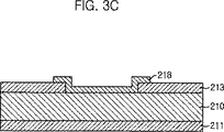
【0020】
次いで、図3Cを参照すれば、ウィンドウ219及びパターニングされた絶縁膜213上に金属パターンを形成する。該金属パターンは、ウィンドウ219上に形成されるヒータ線216及び感知線218、そしてパターニングされた絶縁膜213上に形成される金属パッド214a、214b、214c、214dから構成される。ここで、ヒータ線216は、上記したように、本発明において用いるセラミックバルク222に熱を供給するための抵抗線を形成し、感知線218は、セラミックバルク222の抵抗の変化を測定するために形成されるものである。そして、金属パッド214a、214b、214c、214dは、パターニングされた絶縁膜213上に形成されてシリコン基板210と電気的に絶縁される。また、金属パッド214a、214b、214c、214dは、ヒータ線216及び感知線218を支持するのみでなく、ヒータ線216及び感知線218を外部の電源及び他の外部回路に接続するための手段を提供する。このような金属パターンは、二つの金属パッド214a、214bとヒータ線216とが一体的に形成され、二つの金属パッド214c、214dと感知線218とが一体的に形成されることが製造の容易性の観点から好ましく、0.1〜20μm、特に5μmの厚さに形成されることが好ましい。金属パターンの材料には白金(Pt)を用いるか、パラジウム(Pd)または金(Au)がドープされたニッケル(Ni)、またはホウ素(B)がドープされた多結晶シリコンを用いることができる。また、金属パターンとパターニングされた絶縁膜213との接着性を向上させるために、白金にクロムを付着して用いることができる。この場合、クロムの厚さは0.02μm程度にすることが好ましい。
【0021】
次に、図3Dを参照すれば、シリコン基板210全体をアルカリ水溶液に浸漬し、所定の深さとなるようにウィンドウ219を介して露出しているシリコン基板210をパターニングする。この場合、シリコン酸化膜のような絶縁膜と白金のような金属パターンは、アルカリ水溶液によってエッチングされないことから、シリコン基板210に所定の深さのくぼみ220が形成されることになる。したがって、図3D及び図2に示すように、ヒータ線216及び感知線218は、くぼみ220によってシリコン基板210から分離される。このとき用いられるアルカリ水溶液には、水酸化カリウムまたはエチレンジアミン及びピロカテコール(pyrocatechol)の混合水溶液を用いることができる。例えば、80℃の水酸化カリウムのエッチング溶液に上記のシリコン基板210を2時間浸漬することによって、約150μmの深さのくぼみ220が得られる。
【0022】
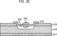
次に、図3Eを参照すれば、ペースト形状のセラミック前駆体滴をヒータ線216及び感知線218の所定部分上に滴下した後、熱処理してセラミックバルク222を形成する。ここで、上記のセラミック前駆体には、例えば、感知物質としてSnO2を90重量%、バインダとして疏水性シリカゾルを9重量%、及び触媒としてPdCl2を1重量%含む混合物を用いることができる。このようなセラミック前駆体に、例えば、エチルセルロースが5%含まれたα−テルピネオールを所定量添加して粘度が数百cps程度になるようにする。次いで、ペースト形状に作られた前駆体をヒータ線216及び感知線218上に滴下する。セラミック前駆体滴を滴下した後に施す熱処理の条件は、上記のセラミックペーストに含まれている溶媒を揮発させることができれば特に限定されない。
【0023】
上記したように、本発明に係るセラミックガスセンサは、セラミックバルクを除いては半導体製造技術に基づいたマイクロマシニング加工によって形成される。したがって、本発明に係るガスセンサ200のヒータ線216及び感知線218、そしてセラミックバルク222の体積は非常に小さい。しかも、ヒータ線216、感知線218及びセラミックバルク222がシリコン基板から分離されているため、熱容量が小さく、熱損失が小さい。また、本発明に係るセラミックガスセンサ200では、セラミックバルク222を感知物質として用いることから、薄膜セラミックを用いる他のセンサに比べて感知特性及び物理的特性に優れている。また、本発明に係るガスセンサ200の製造方法においては、ウィンドウ219の形成及び金属パターンの形成のために、2枚のマスクのみが必要である。また、半導体加工技術の長所であるバッチ工程における生産がそのまま適用されるので、ガスセンサの製造コストを低減できる。
【0024】
一方、図4A〜図4Fは、本発明に係る他の実施の形態である、ヒータ線、感知線及びセラミックバルクからなるガスセンサの感知部を示している。図2に示すように、ヒータ線216及び感知線218が互いに平行の直線状に形成されており、その上にセラミックバルク222が位置する場合には、抵抗がヒータ線216全体に均一に分布することから、発生した熱の一部のみがセラミックバルク222の加熱に用いられ、セラミックバルク222の温度分布は不均一になる。このような問題点は、図4A〜図4Fに示すように、感知部の構造を変形させることによって改善できる。
【0025】
図4Aにはヒータ線316がU字状に曲がっており、その間に感知線318の分岐線318aが挿入された例が示されている。このような構造によれば、セラミックバルク322部分に抵抗が集中するのみでなく、熱がセラミックバルク322に均一に拡散するので、上記の問題が改善されてガスセンサの感知特性がより一層改善され、熱損失がさらに低減することになる。また、このようなセラミックバルク322の抵抗集中とセラミックバルク322での熱の均一な分布をさらに改善するために、図4Bに示したように、ヒータ線416をジグザグ形状に折り曲げて設け、感知線418の分岐線418aをヒータ線416の片側から凹形状のヒータ線416の間に挿入するか、図4Cに示すように、ヒータ線516をジグザグ形状に折り曲げて設け、2つの感知線518の分岐線518aを、ヒータ線516の両側から凹形状のヒータ線516の間に挿入することもできる。
【0026】
図4D〜4Fに示すように、セラミックバルク622、722、822の抵抗率変化が、主としてセラミックバルク622、722、822を均一に加熱することに依存することから、セラミックバルク622、722、822内におけるヒータ線616、716、816を感知線618、718、818よりも厚く形成している。したがって、本発明の実施の形態においては、感知線618、718、818の幅は約10μmに、厚さは約5μmに構成することが好ましい。また、感知線618、718、818の幅が約10μmであり、厚さが約5μmである場合には、ヒータ線616、716、816の幅は約20μmであって、厚さは約5μmであるものが好ましい。
【0027】
以上のように、本発明は、ヒータ線がシリコン基板から分離され感知物質であるセラミックをバルク形状に形成することによって、熱容量及び熱損失を最小化し、低電力及び低コストのガスセンサが得られるという利点を有する。
【0028】
したがって、本発明に係るガスセンサは、エネルギー源が制限される携帯用ガス感知装置などに広く適用することができる。また、従来技術に比べて、本発明のガスセンサの製造方法は、ウィンドウの形成及び金属パターンの形成のためのパターニングに2枚のマスクのみが必要であり、半導体加工技術の長所であるバッチ工程における生産がそのまま適用され得ることから、低コストでガスセンサを製造できるという長所を有する。
【0029】
尚、本発明は、本実施の形態に限られるものではなく、本発明の趣旨から逸脱しない範囲内において多様に変更して実施され得るものである。
【図面の簡単な説明】
【図1】 図1は、従来のガスセンサの断面図である。
【図2】 図2は、本発明に係るガスセンサを示す斜視図である。
【図3A】 図3Aは、本発明に係るガスセンサの製造方法を説明する図2の線分I−Iに沿った断面図である。
【図3B】 図3Bは、本発明に係るガスセンサの製造方法を説明する図2の線分I−Iに沿った断面図である。
【図3C】 図3Cは、本発明に係るガスセンサの製造方法を説明する図2の線分I−Iに沿った断面図である。
【図3D】 図3Dは、本発明に係るガスセンサの製造方法を説明する図2の線分I−Iに沿った断面図である。
【図3E】 図3Eは、本発明に係るガスセンサの製造方法を説明する図2の線分I−Iに沿った断面図である。
【図4A】 図4Aは、本発明に係るガスセンサの感知部を示す断面図である。
【図4B】 図4Bは、本発明に係るガスセンサの感知部を示す断面図である。
【図4C】 図4Cは、本発明に係るガスセンサの感知部を示す断面図である。
【図4D】 図4Dは、本発明に係るガスセンサの感知部を示す断面図である。
【図4E】 図4Eは、本発明に係るガスセンサの感知部を示す断面図である。
【図4F】 図4Fは、本発明に係るガスセンサの感知部を示す断面図であ[0001]
【Technical field】
The present invention relates to a gas sensor and a manufacturing method thereof, and more particularly, a heater line and a sensing line are formed separately from a substrate using a semiconductor manufacturing process, and a ceramic bulk as a gas sensing material is formed on the heater line and the sensing line. The present invention relates to a low-power gas sensor having a small heat capacity and heat loss and excellent sensing characteristics, and a method for manufacturing the same.
[0002]
[Background]
Generally, the ceramic gas sensor is for detecting a specific gas. When the gas sensor is exposed to a specific gas, the conductivity of the ceramic that is a gas sensing material changes or an electromotive force is generated. Therefore, a specific gas can be detected by measuring such a change in conductivity or electromotive force. In such a ceramic gas sensor, in order to improve the sensitivity and the degree of separation with respect to a specific gas, it is desirable not only to dope the ceramic with a catalyst material but also to maintain a high temperature of 300 ° C. or higher. Therefore, the ceramic gas sensor consumes more power than other sensors. In order to expand the application range of the ceramic gas sensor, it is very important to provide a low power ceramic gas sensor that can maintain a high temperature with a small energy.
[0003]
FIG. 1 is a cross-sectional view illustrating a
[0004]
Since the
[0005]
DISCLOSURE OF THE INVENTION
Accordingly, it is an object of the present invention to form the heater line and the sensing line separately from the silicon substrate, and to form the gas sensing material ceramic in a bulk shape extended on the heater line and the sensing line. Accordingly, it is an object of the present invention to provide a gas sensor with improved sensing characteristics and minimized heat capacity and heat loss of heater wires and sensing substances.
[0006]
Another object of the present invention is to provide a method for manufacturing a gas sensor with improved sensing characteristics and minimized heat capacity and heat loss.
[0007]
According to an embodiment of the present invention, a silicon substrate having a recess formed by patterning to a predetermined depth, an insulating film formed on the silicon substrate excluding the recess, and the recess A first conductive pattern that is fixed to the insulating film across and electrically insulated from the silicon substrate, and is fixed to the insulating film across the depression and electrically connected to the silicon substrate and the first conductive pattern. Provided is a gas sensor comprising an insulated second conductive pattern and a gas sensing part formed in a predetermined portion of the first and second conductive patterns.
[0008]
Another embodiment of the present invention includes a step of forming an insulating film on a silicon substrate, a step of patterning a part of the insulating film to form a window, and a silicon substrate exposed by the insulating film and the window. Forming the first and second metal patterns, and patterning the silicon substrate exposed to the window by immersing the silicon substrate in an alkaline aqueous solution to form the window-shaped depressions. And a step of separating the second conductive pattern from the silicon substrate, and a step of forming a gas sensing portion in a predetermined portion of the first and second conductive patterns formed on the recess. I will provide a.
[0009]
BEST MODE FOR CARRYING OUT THE INVENTION
Hereinafter, embodiments of the present invention will be described in detail with reference to the accompanying drawings.
[0010]
FIG. 2 shows a perspective view of a
[0011]
As shown in FIG. 2, the
[0012]
Such a metal pattern is formed of platinum (Pt) or a polycrystalline silicon film doped with nickel (Ni) or boron (B) coated with a noble metal such as gold or palladium (Pd). It is preferable. The thickness is preferably about 0.1 to 20 μm, particularly about 5 μm. A
[0013]
The operation of the ceramic gas sensor described above will be described as follows. If a current is supplied to the
[0014]
An example of a method for measuring the resistivity of the
V out ≒ [R s / (R 1 + R s )] × V cc
[0015]
Here, for the sake of convenience of explanation, an approximate value of the resistance (R s ) of the
[0016]
Therefore, since the change in the resistivity of the
[0017]
Next, FIGS. 3A to 3E are cross-sectional views illustrating a process of manufacturing the gas sensor according to the present invention.
[0018]
Referring to FIG. 3A, insulating
[0019]
Next, referring to FIG. 3B, a central portion of the insulating
[0020]
Next, referring to FIG. 3C, a metal pattern is formed on the
[0021]
Next, referring to FIG. 3D, the
[0022]
Next, referring to FIG. 3E, a paste-shaped ceramic precursor droplet is dropped on predetermined portions of the
[0023]
As described above, the ceramic gas sensor according to the present invention is formed by a micromachining process based on a semiconductor manufacturing technique except for a ceramic bulk. Therefore, the volume of the
[0024]
On the other hand, FIGS. 4A to 4F show a sensing unit of a gas sensor including a heater wire, a sensing wire, and a ceramic bulk according to another embodiment of the present invention. As shown in FIG. 2, when the
[0025]
FIG. 4A shows an example in which the
[0026]
As shown in FIGS. 4D-4F, the change in resistivity of the ceramic bulks 622, 722, 822 is primarily dependent on uniform heating of the ceramic bulks 622, 722, 822, and therefore within the ceramic bulks 622, 722, 822. The heater lines 616, 716, and 816 are formed thicker than the sense lines 618, 718, and 818. Therefore, in the embodiment of the present invention, it is preferable that the width of the
[0027]
As described above, according to the present invention, a heater wire is separated from a silicon substrate and a ceramic as a sensing material is formed in a bulk shape, thereby minimizing heat capacity and heat loss and obtaining a low power and low cost gas sensor. Have advantages.
[0028]
Therefore, the gas sensor according to the present invention can be widely applied to portable gas sensing devices and the like in which energy sources are limited. Compared with the prior art, the gas sensor manufacturing method of the present invention requires only two masks for patterning for forming the window and forming the metal pattern. In the batch process, which is an advantage of the semiconductor processing technology. Since production can be applied as it is, it has an advantage that a gas sensor can be manufactured at low cost.
[0029]
It should be noted that the present invention is not limited to the present embodiment, and can be implemented with various modifications without departing from the spirit of the present invention.
[Brief description of the drawings]
FIG. 1 is a cross-sectional view of a conventional gas sensor.
FIG. 2 is a perspective view showing a gas sensor according to the present invention.
FIG. 3A is a cross-sectional view taken along line I-I in FIG. 2 for explaining a method for manufacturing a gas sensor according to the present invention.
FIG. 3B is a cross-sectional view taken along the line I-I in FIG. 2 for explaining the gas sensor manufacturing method according to the present invention.
FIG. 3C is a cross-sectional view taken along the line I-I in FIG. 2 for explaining the gas sensor manufacturing method according to the present invention.
FIG. 3D is a cross-sectional view taken along the line II in FIG. 2 for explaining the method for manufacturing the gas sensor according to the present invention.
FIG. 3E is a cross-sectional view taken along the line II in FIG. 2 for explaining the method for manufacturing the gas sensor according to the present invention.
FIG. 4A is a cross-sectional view showing a sensing part of a gas sensor according to the present invention.
FIG. 4B is a cross-sectional view showing a sensing part of the gas sensor according to the present invention.
FIG. 4C is a cross-sectional view showing a sensing unit of the gas sensor according to the present invention.
FIG. 4D is a cross-sectional view showing a sensing part of the gas sensor according to the present invention.
FIG. 4E is a cross-sectional view showing a sensing part of the gas sensor according to the present invention.
FIG. 4F is a cross-sectional view showing a sensing unit of the gas sensor according to the present invention.
Claims (11)
前記くぼみ以外の前記シリコン基板上に形成された絶縁膜と、
前記くぼみを横切り、前記絶縁膜に固定され、前記シリコン基板と電気的に絶縁された第1導電パターンと、
前記くぼみを横切り、前記絶縁膜に固定され、前記シリコン基板及び前記第1導電パターンと電気的に絶縁された第2導電パターンと、
前記第1及び第2導電パターンの所定部分に形成されたガス感知部と
を備え、
前記第1導電パターンが、前記ガス感知部に熱を供給するために用いられ、前記ガス感知部の内部に少なくとも1つの凹形状空間を形成するように屈曲し、
前記第2導電パターンが、ガスの状態に応じてガス感知部の変化を感知するための感知線として用いられ、前記凹形状空間に挿入される分岐部を有することを特徴とするガスセンサ。A silicon substrate with indentations formed by patterning to a predetermined depth;
An insulating film formed on the silicon substrate other than the depression;
A first conductive pattern traversing the depression, fixed to the insulating film , and electrically insulated from the silicon substrate;
A second conductive pattern traversing the depression, fixed to the insulating film, and electrically insulated from the silicon substrate and the first conductive pattern;
A gas sensing part formed on a predetermined portion of the first and second conductive patterns ,
The first conductive pattern is used to supply heat to the gas sensing unit, and is bent to form at least one concave space in the gas sensing unit;
The gas sensor according to claim 1, wherein the second conductive pattern is used as a sensing line for sensing a change in the gas sensing unit according to a gas state, and has a branch part inserted into the concave space .
前記絶縁膜の一部分をパターニングしてウィンドウを形成する工程と、
前記絶縁膜及びウィンドウによって露出されたシリコン基板の上に第1及び第2金属パターンを形成する工程と、
前記シリコン基板をアルカリ水溶液に浸漬し、前記ウィンドウに露出されたシリコン基板をパターニングして前記ウィンドウ形状のくぼみを形成することによって、前記第1及び第2導電パターンを前記シリコン基板から分離させる工程と、
前記くぼみの上方に形成された前記第1及び第2導電パターンの所定部分にガス感知部を形成する工程と
を含み、
前記第1導電パターンが、前記ガス感知部に熱を供給するために用いられ、前記ガス感知部の内部に少なくとも1つの凹形状空間を形成するように屈曲し、
前記第2導電パターンが、ガスの状態に応じてガス感知部の変化を感知するための感知線として用いられ、前記凹形状空間に挿入される分岐部を有することを特徴とするガスセンサの製造方法。Forming an insulating film on the silicon substrate;
Patterning a portion of the insulating film to form a window;
Forming first and second metal patterns on the silicon substrate exposed by the insulating layer and the window;
Separating the first and second conductive patterns from the silicon substrate by immersing the silicon substrate in an alkaline aqueous solution and patterning the silicon substrate exposed in the window to form the window-shaped depressions; ,
Look including a step of forming a gas sensing portion at a predetermined portion of said first and second conductive patterns formed over the recess,
The first conductive pattern is used to supply heat to the gas sensing unit, and is bent to form at least one concave space in the gas sensing unit;
The method of manufacturing a gas sensor, wherein the second conductive pattern is used as a sensing line for sensing a change of the gas sensing unit according to a gas state, and has a branch part inserted into the concave space. .
Applications Claiming Priority (3)
| Application Number | Priority Date | Filing Date | Title |
|---|---|---|---|
| KR1019990045306A KR20010037655A (en) | 1999-10-19 | 1999-10-19 | Low Power type Ceramic Gas Sensor Fabricated by Micromachining Technology and Fabrication Method Thereof |
| KR1999/45306 | 1999-10-19 | ||
| PCT/KR2000/001161 WO2001028915A1 (en) | 1999-10-19 | 2000-10-17 | Gas sensor and fabrication method thereof |
Publications (2)
| Publication Number | Publication Date |
|---|---|
| JP2003512606A JP2003512606A (en) | 2003-04-02 |
| JP3682603B2 true JP3682603B2 (en) | 2005-08-10 |
Family
ID=19615914
Family Applications (1)
| Application Number | Title | Priority Date | Filing Date |
|---|---|---|---|
| JP2001531713A Expired - Fee Related JP3682603B2 (en) | 1999-10-19 | 2000-10-17 | Gas sensor and manufacturing method thereof |
Country Status (10)
| Country | Link |
|---|---|
| US (1) | US6997040B1 (en) |
| EP (1) | EP1226090B1 (en) |
| JP (1) | JP3682603B2 (en) |
| KR (2) | KR20010037655A (en) |
| CN (1) | CN1272235C (en) |
| AT (1) | ATE372297T1 (en) |
| AU (1) | AU7967500A (en) |
| DE (1) | DE60036301D1 (en) |
| TW (1) | TW506942B (en) |
| WO (1) | WO2001028915A1 (en) |
Families Citing this family (25)
| Publication number | Priority date | Publication date | Assignee | Title |
|---|---|---|---|---|
| DE10144343A1 (en) * | 2001-09-10 | 2003-03-27 | Perkinelmer Optoelectronics | Sensor for contactless measurement of a temperature |
| CN1938588B (en) * | 2004-01-27 | 2011-11-09 | H2Scan公司 | Isolated gas sensor configuration |
| US7389672B2 (en) * | 2004-01-27 | 2008-06-24 | H2Scan Corporation | Method and apparatus for thermal isolation of a gas sensor |
| KR20050081691A (en) * | 2004-02-16 | 2005-08-19 | 세주엔지니어링주식회사 | Method for manufacturing micro-structure catalytic combustion type gas sensor, and gas sensor using the micro-structure catalytic combustion gas sensor |
| KR100773025B1 (en) * | 2004-02-27 | 2007-11-05 | 이엠씨마이크로시스템 주식회사 | Semiconductor gas sensor, its driving method and fabrication method |
| KR101119756B1 (en) * | 2005-04-20 | 2012-03-23 | 매그나칩 반도체 유한회사 | Semiconductor devices |
| JP5144090B2 (en) * | 2007-02-26 | 2013-02-13 | シチズンホールディングス株式会社 | Catalytic combustion type gas sensor and manufacturing method of catalytic combustion type gas sensor |
| KR100942439B1 (en) * | 2007-12-28 | 2010-02-17 | 전자부품연구원 | Fabricating method for micro gas sensor and the same |
| JP5202007B2 (en) * | 2008-01-29 | 2013-06-05 | 日立オートモティブシステムズ株式会社 | Thermal fluid flow sensor |
| TWI434037B (en) | 2010-12-03 | 2014-04-11 | Ind Tech Res Inst | Gas sensor and fabricating method thereof |
| KR101774757B1 (en) * | 2011-10-13 | 2017-09-07 | 한국전자통신연구원 | Gas Sensor, Method of Making and Using The Same |
| KR101431471B1 (en) * | 2013-05-10 | 2014-08-21 | 한국과학기술원 | Low power consumption type gas sensor |
| KR101532557B1 (en) | 2014-05-09 | 2015-06-30 | 부경대학교 산학협력단 | LED chip with built-in hybrid sensor and maunfacturing method thereof |
| KR101666572B1 (en) * | 2014-11-03 | 2016-10-17 | 한국과학기술원 | Hot sensor package |
| KR20160061842A (en) * | 2014-11-24 | 2016-06-01 | 엘지이노텍 주식회사 | Gas Sensor Package and Manufacturing Method thereof |
| US11391709B2 (en) | 2016-08-18 | 2022-07-19 | Carrier Corporation | Isolated sensor and method of isolating a sensor |
| CN107782767B (en) * | 2016-08-26 | 2022-01-07 | 深迪半导体(绍兴)有限公司 | Heating plate of gas sensor and processing method |
| KR102359236B1 (en) * | 2016-08-31 | 2022-02-07 | 엘지이노텍 주식회사 | Gas sensing module and sensing device |
| KR102519644B1 (en) * | 2016-09-22 | 2023-04-10 | 엘지이노텍 주식회사 | Gas sensing module, gas sensing apparatus |
| CN107089638A (en) * | 2017-04-24 | 2017-08-25 | 广东美的制冷设备有限公司 | Microheater and its processing method |
| CN108918599B (en) * | 2018-05-08 | 2022-01-11 | 中芯集成电路(宁波)有限公司 | Gas sensor and forming method thereof |
| WO2020235118A1 (en) * | 2019-05-21 | 2020-11-26 | パナソニックIpマネジメント株式会社 | Gas sensor |
| US11353381B1 (en) * | 2020-06-09 | 2022-06-07 | Applied Materials, Inc. | Portable disc to measure chemical gas contaminants within semiconductor equipment and clean room |
| KR102468714B1 (en) * | 2020-08-07 | 2022-11-21 | 울산과학기술원 | Ultra-low power gas sensor based on suspended nano structure and manufacturing method thereof |
| DE102020122923A1 (en) | 2020-09-02 | 2022-03-03 | Tdk Electronics Ag | Sensor element and method for manufacturing a sensor element |
Family Cites Families (16)
| Publication number | Priority date | Publication date | Assignee | Title |
|---|---|---|---|---|
| CA1216330A (en) * | 1983-02-07 | 1987-01-06 | Junji Manaka | Low power gas detector |
| US4688015A (en) | 1983-10-28 | 1987-08-18 | Ngk Spark Plug Co., Ltd. | Gas sensor with ceramics substrate having surface-carried ceramics particles |
| JPS63259459A (en) | 1987-04-17 | 1988-10-26 | Toshiba Corp | Limiting current type gas sensor |
| JPH01299452A (en) * | 1988-05-27 | 1989-12-04 | Ricoh Co Ltd | Four-terminal detecting type gas detector |
| JPH01313751A (en) | 1988-06-13 | 1989-12-19 | Figaro Eng Inc | Gas sensor |
| US4953387A (en) * | 1989-07-31 | 1990-09-04 | The Regents Of The University Of Michigan | Ultrathin-film gas detector |
| US5763782A (en) * | 1992-03-16 | 1998-06-09 | British Technology Group Limited | Micromechanical sensor |
| US5387329A (en) * | 1993-04-09 | 1995-02-07 | Ciba Corning Diagnostics Corp. | Extended use planar sensors |
| JP3201881B2 (en) | 1993-06-04 | 2001-08-27 | 株式会社トクヤマ | Gas sensor |
| AU7820194A (en) * | 1993-10-08 | 1995-05-04 | Csir | A catalytic gas sensor |
| DE4423289C1 (en) * | 1994-07-02 | 1995-11-02 | Karlsruhe Forschzent | Gas sensor for reducing or oxidizing gases |
| US5565084A (en) | 1994-10-11 | 1996-10-15 | Qnix Computer Co., Ltd. | Electropolishing methods for etching substrate in self alignment |
| FR2736205B1 (en) | 1995-06-30 | 1997-09-19 | Motorola Semiconducteurs | SEMICONDUCTOR SENSOR DEVICE AND ITS FORMING METHOD |
| JP3570644B2 (en) | 1995-11-14 | 2004-09-29 | フィガロ技研株式会社 | Gas sensor |
| JPH11166942A (en) | 1997-09-30 | 1999-06-22 | Honda Motor Co Ltd | Gas rate sensor |
| JP3472865B2 (en) * | 1998-03-09 | 2003-12-02 | 本田技研工業株式会社 | Manufacturing method of gas rate sensor |
-
1999
- 1999-10-19 KR KR1019990045306A patent/KR20010037655A/en active Search and Examination
-
2000
- 2000-10-17 KR KR10-2002-7002442A patent/KR100438190B1/en active IP Right Grant
- 2000-10-17 JP JP2001531713A patent/JP3682603B2/en not_active Expired - Fee Related
- 2000-10-17 CN CNB008145342A patent/CN1272235C/en not_active Expired - Fee Related
- 2000-10-17 AT AT00970275T patent/ATE372297T1/en not_active IP Right Cessation
- 2000-10-17 WO PCT/KR2000/001161 patent/WO2001028915A1/en active IP Right Grant
- 2000-10-17 AU AU79675/00A patent/AU7967500A/en not_active Abandoned
- 2000-10-17 US US10/110,209 patent/US6997040B1/en not_active Expired - Fee Related
- 2000-10-17 EP EP00970275A patent/EP1226090B1/en not_active Expired - Lifetime
- 2000-10-17 DE DE60036301T patent/DE60036301D1/en not_active Expired - Lifetime
-
2001
- 2001-04-13 TW TW090109078A patent/TW506942B/en not_active IP Right Cessation
Also Published As
| Publication number | Publication date |
|---|---|
| JP2003512606A (en) | 2003-04-02 |
| EP1226090A4 (en) | 2003-07-16 |
| EP1226090A1 (en) | 2002-07-31 |
| AU7967500A (en) | 2001-04-30 |
| EP1226090B1 (en) | 2007-09-05 |
| DE60036301D1 (en) | 2007-10-18 |
| US6997040B1 (en) | 2006-02-14 |
| KR20010037655A (en) | 2001-05-15 |
| CN1379731A (en) | 2002-11-13 |
| TW506942B (en) | 2002-10-21 |
| ATE372297T1 (en) | 2007-09-15 |
| KR100438190B1 (en) | 2004-07-02 |
| CN1272235C (en) | 2006-08-30 |
| KR20020060694A (en) | 2002-07-18 |
| WO2001028915A1 (en) | 2001-04-26 |
Similar Documents
| Publication | Publication Date | Title |
|---|---|---|
| JP3682603B2 (en) | Gas sensor and manufacturing method thereof | |
| JPS6323500B2 (en) | ||
| JPH01109250A (en) | Gas sensor | |
| JP2022530944A (en) | Heat ray type gas sensor chip, sensor and manufacturing method of sensor | |
| JP2018063241A (en) | Gas sensor | |
| JPS6118854A (en) | Oxygen concentration detecting element | |
| JPH11153571A (en) | Oxygen sensor element | |
| JPH08278274A (en) | Gas sensor and preparation thereof | |
| US20230021048A1 (en) | Vaporisation device for an electronic inhaler and method of producing a vaporisation device | |
| KR100929025B1 (en) | Plasma contact-fired hydrogen and combustible gas sensor and method of manufacturing the same | |
| KR100906496B1 (en) | Gas sensor and method for manufacturing the same | |
| JP4798961B2 (en) | HEATER DEVICE AND GAS SENSOR DEVICE USING THE SAME | |
| JPH04507461A (en) | Self-holding thin film filament sensor, its formation method, and application to gas detectors and gas chromatography | |
| JP2004037402A (en) | Thin film gas sensor | |
| CN115308270A (en) | Palladium alloy film hydrogen sensor and preparation method and use method thereof | |
| KR101992022B1 (en) | Semiconductor gas sensor | |
| KR100773025B1 (en) | Semiconductor gas sensor, its driving method and fabrication method | |
| EP3726208A1 (en) | High surface area electrode for electrochemical sensor | |
| JPS6124649B2 (en) | ||
| TWI373615B (en) | ||
| KR20080062964A (en) | Gas sensor using nano material and method for preparing the same | |
| JP2004037224A (en) | Gas sensor, gas leakage alarm using the same, gas leakage alarm system, and manufacturing method of gas sensor | |
| JP2000019139A (en) | Ceramic chlorine gas sensor | |
| CN117214248A (en) | Low-power-consumption silicon-based MEMS gas sensor chip and preparation method thereof | |
| JP2984095B2 (en) | Gas sensor manufacturing method |
Legal Events
| Date | Code | Title | Description |
|---|---|---|---|
| A711 | Notification of change in applicant |
Free format text: JAPANESE INTERMEDIATE CODE: A712 Effective date: 20040122 |
|
| RD03 | Notification of appointment of power of attorney |
Free format text: JAPANESE INTERMEDIATE CODE: A7423 Effective date: 20040122 |
|
| A521 | Request for written amendment filed |
Free format text: JAPANESE INTERMEDIATE CODE: A821 Effective date: 20040122 |
|
| A131 | Notification of reasons for refusal |
Free format text: JAPANESE INTERMEDIATE CODE: A131 Effective date: 20040901 |
|
| A601 | Written request for extension of time |
Free format text: JAPANESE INTERMEDIATE CODE: A601 Effective date: 20041130 |
|
| A602 | Written permission of extension of time |
Free format text: JAPANESE INTERMEDIATE CODE: A602 Effective date: 20041213 |
|
| A521 | Request for written amendment filed |
Free format text: JAPANESE INTERMEDIATE CODE: A523 Effective date: 20050301 |
|
| TRDD | Decision of grant or rejection written | ||
| A01 | Written decision to grant a patent or to grant a registration (utility model) |
Free format text: JAPANESE INTERMEDIATE CODE: A01 Effective date: 20050413 |
|
| A61 | First payment of annual fees (during grant procedure) |
Free format text: JAPANESE INTERMEDIATE CODE: A61 Effective date: 20050510 |
|
| R150 | Certificate of patent or registration of utility model |
Free format text: JAPANESE INTERMEDIATE CODE: R150 |
|
| R154 | Certificate of patent or utility model (reissue) |
Free format text: JAPANESE INTERMEDIATE CODE: R154 |
|
| FPAY | Renewal fee payment (event date is renewal date of database) |
Free format text: PAYMENT UNTIL: 20090603 Year of fee payment: 4 |
|
| FPAY | Renewal fee payment (event date is renewal date of database) |
Free format text: PAYMENT UNTIL: 20100603 Year of fee payment: 5 |
|
| FPAY | Renewal fee payment (event date is renewal date of database) |
Free format text: PAYMENT UNTIL: 20110603 Year of fee payment: 6 |
|
| LAPS | Cancellation because of no payment of annual fees |