JP3679695B2 - Developing apparatus, substrate processing apparatus, and developing method - Google Patents
Developing apparatus, substrate processing apparatus, and developing method Download PDFInfo
- Publication number
- JP3679695B2 JP3679695B2 JP2000242808A JP2000242808A JP3679695B2 JP 3679695 B2 JP3679695 B2 JP 3679695B2 JP 2000242808 A JP2000242808 A JP 2000242808A JP 2000242808 A JP2000242808 A JP 2000242808A JP 3679695 B2 JP3679695 B2 JP 3679695B2
- Authority
- JP
- Japan
- Prior art keywords
- substrate
- unit
- gas
- wafer
- developer
- Prior art date
- Legal status (The legal status is an assumption and is not a legal conclusion. Google has not performed a legal analysis and makes no representation as to the accuracy of the status listed.)
- Expired - Fee Related
Links
Images


Description
【0001】
【発明の属する技術分野】
本発明は、例えば基板に対して現像処理等の基板処理を行う現像装置及びその方法に関する。
【0002】
【従来の技術】
半導体ウエハ(以下「ウエハ」という)や液晶ディスプレイのガラス基板(LCD基板)の表面に所定のパタ−ンを形成するためのマスクは、ウエハ等の基板表面にレジストを塗布した後、光、電子線あるいはイオン線等をレジスト面に照射し、現像することによって得られる。ここで現像処理は、露光工程にて光等が照射された部分あるいは照射されない部分をアルカリ水溶液等により溶解するものであり、従来では図18に示す方法により行われている。
【0003】
即ちこの従来方法においては、真空吸着機能を備えたスピンチャック11の上に基板例えばウエハWを吸着保持し、ウエハWの直径に対応する長さに沿って多数の吐出孔12が配列された供給ノズル13を、ウエハWの中央部にて吐出孔12がウエハ表面から例えば1mm上方になるように位置させる。そして吐出孔12から現像液10をウエハ表面の中央部に供給して図18に示すように液盛りを行い、続いて吐出孔12から現像液10の供給を行いながら、ウエハWを半回転(180度回転)させる。
【0004】
こうすることによってウエハ中央部にはじめに液盛りされた現像液10が広げられると同時に現像液10が新たに供給され、この結果ウエハ表面全体に現像液10の液膜が所定の厚さで形成されることになる。こうして現像液10の液盛りを行った後例えば60秒間放置し、次いでウエハ表面にリンス液を供給して現像液を洗い流すことにより現像が行われる。
【0005】
ここでこのような現像処理が行われる従来の現像装置について図19により簡単に説明すると、前記スピンチャック11の周りは、現像液10の飛散を防止するためのカップ14で覆われており、このカップ14の上方側にはフィルタとファンとを組み合わせて構成されたフィルタユニット15が設けられていると共に、フィルタユニット15とカップ14との間には多数の通気孔16aが形成された整流板16が設けられている。
【0006】
前記カップ14には排気路17が接続されており、排気路17にて排気された空気の一部が、不純物の除去や、所定の温度及び湿度への調整を行う図示しないフィルタ装置を介してフィルタユニット15に循環供給され、フィルタユニット15からカップ14に向かってダウンフロ−を形成しながら供給されるようになっている。そしてフィルタユニット15からの、不純物が除去され、所定の温度及び湿度に調整された空気は、整流板16を通過し、これにより均一性が高められた状態でカップ14側へ供給されるようになっている。このように高精度に調整された空気のダウンフロ−を形成するのは、現像液温度および蒸発速度均一化のためである。
【0007】
【発明が解決しようとする課題】
しかしながら例えばI線レジストを用いた場合、上述の現像方法では現像ムラが発生し、部位によって現像線幅が変わってしまい、例えばウエハ中央領域と周縁領域との間では、約4nm程度線幅が狂ってしまうという問題がある。この原因について検討してみると、現像の進行の度合いは現像液10の温度に依存することから、ウエハ面内において現像液10に温度分布が発生していると考えられる。
【0008】
つまり現像液10は例えば23℃程度の温度に調整されているが、ウエハWに液盛りを行って放置している間に現像液Dに含まれる水分が蒸発し、これにより現像液10の潜熱が奪われるので、現像液10の温度は時間と共に低下する。一方、既述の高精度に調整された空気のダウンフロ−の形成により、ウエハWの面内では、周縁領域の温度が中央領域よりも低下してしまうと考えられる。即ちダウンフロ−の形成により、ウエハWから見れば上方側から風が流れてくることになるが、上方側からウエハWに当たった風は、図20に示すようにウエハ面に沿って外周側に向かって流れ、周縁領域の方が中央領域よりも風量が多くなる。このためウエハWの面内では周縁領域の方が中央領域よりも気化熱が多くなるので、周縁領域の放熱量が中央領域よりも大きくなり、結果として周縁領域の温度の低下の度合いが大きいと推察される。
【0009】
このためリンス開始時にはウエハ中央領域と周縁領域との間に例えば約1℃程度の現像液10の温度差が生じ、これにより現像状態にムラが生じて、出来上がり寸法が変化するという悪影響が発生していると推察される。
【0010】
本発明はこのような事情の下になされたものであり、その目的は現像時に現像液の温度を基板の面内でほぼ均一にすることにより、現像液の温度差による現像ムラの発生を抑えて、処理の均一性を高める現像装置及びその方法を提供することにある。
【0011】
【課題を解決するための手段】
このため、本発明の現像装置は、基板の表面に向かう気流が形成された雰囲気内で、前記基板表面に現像液を液盛りして現像を行う現像装置において、前記基板を保持するための基板保持部と、基板に現像液を供給するための供給部と、前記基板保持部に保持された基板の表面側に、基板と対向するように設けられ、第1の通気孔が形成された第1の整流板と、前記第1の整流板と相対的に面方向に移動できるように、この第1の整流板と対向するように設けられ、第2の通気孔が形成された第2の整流板と、を備え、前記保持された基板に現像液が供給され、前記基板の現像が行われる間に、前記第1の整流板と第2の整流板とを相対的に面方向に移動させ、第1の通気孔と、第2の整流板の第2の通気孔が形成されていない領域とを面方向に直交する方向に重ねることにより第1の通気孔の大きさを調整し、前記第1の通気孔の大きさを基板の周縁領域よりも中央近傍領域側を大きくし、基板表面の中央近傍領域に当たる風の風量を周縁領域よりも多くすることを特徴とする。
【0012】
このような現像装置では、基板表面に当たる風の風量を制御することができるので、基板表面への風量に応じて変化する基板上の現像液の気化熱を調整でき、結果的に基板上の現像液の温度を制御することができる。
【0013】
具体的には、前記第1の通気孔の大きさを、基板上に現像液を液盛りした状態のままにして基板表面の現像を行うときには、基板表面に現像液の液盛りを行うときよりも小さくし、前記現像時には前記現像液の液盛り時よりも、基板表面に当たる風の風量を少なくすることが行われ、この場合には現像時に基板表面に風が当たらないようにすることも含まれる。つまりこの現像装置では、基板の表面に向かう気流が形成された雰囲気内で、前記基板表面に現像液を液盛りする工程と、その後基板上に現像液を液盛りした状態のままにして、基板表面に風が当たらないようにしながら基板表面を現像する工程と、を含む現像方法が実施される。
【0014】
このように現像時に基板表面に風が当たらないようにすると、風の影響による基板上の現像液の気化熱の変化が抑えられ、現像液の放熱量が基板の面内においてほぼ均一になる。このため基板上の現像液の温度変化が基板の面内においてほぼ揃えられ、現像液の温度差が原因となる現像ムラの発生が抑えられて、処理の均一性を高めることができる。
【0015】
また本発明では、基板表面への風が当たる領域を調整しながら基板表面を現像するようにしてもよく、例えば前記基板表面の現像を行うときには、第1の通気孔の大きさを、基板の周縁領域よりも中央近傍領域側を大きくして、基板表面の中央近傍領域に当たる風の風量を周縁領域よりも多くするようにしてもよい。ここで基板の中央近傍領域のみに風が当たり、周縁領域には風が当たらない場合も含むものとする。
【0016】
この場合においても、基板に当たった風は基板の表面に沿って周縁領域に向かって流れて行き、基板の表面全体に均一に風が当たる場合には、周縁領域の方が風量が多くなるので、基板表面の中央近傍領域に当たる風の風量を周縁領域よりも多くするようにすることにより、結果として基板に当たる風の風量が基板の面内でほぼ均一になる。このため基板上の現像液の温度変化が基板の面内においてほぼ揃えられるので、現像処理の均一性を高めることができる。
【0017】
【発明の実施の形態】
図1は本発明を現像装置に適用した場合の現像装置の一実施の形態の全体構成を示す縦断面図であり、図中20は現像装置を収納する処理室(現像処理室)をなす処理ケースであって、この処理ケース20の内部には、基板であるウエハWの中央近傍を、被処理面(表面)が上を向くようにほぼ水平な状態で保持すると共に、当該ウエハWを鉛直軸まわりに回転させ、かつ昇降させるための基板保持部をなすウエハ保持部2が設けられている。
【0018】
このウエハ保持部2について図2により説明すると、ウエハ保持部2は例えば真空吸着機能を有し、昇降機構とモ−タとが組み合わされた駆動部21により、回転軸22を介して鉛直軸まわりに回転自在かつ昇降自在に構成されている。こうしてウエハWは、ウエハ保持部2により、図2に示すウエハ保持部2に吸着保持された処理位置と、図中一点鎖線で示す、処理位置よりも上方側のウエハWの受け渡し位置との間で昇降自在、回転自在に保持される。
【0019】
このようなウエハ保持部2の周囲には、前記処理位置にあるウエハWの周囲を囲み、ウエハ上に供給された現像液を振り切る際に、この液が周囲に飛散するのを防ぐための、円形筒状のカップ3が設けられている。カップ3は、外カップ31と内カップ32とからなり、外カップ31は、現像液の飛散を防止するときには、前記ウエハWの受け渡し位置よりも上方側に上端が位置し、ウエハWの受け渡し時や現像液の液盛り時には、前記ウエハWの受け渡し位置よりも下方側に上端が位置するように、図示しない昇降機構により昇降自在に構成されている。
【0020】
内カップ32は外カップ31の内側に、前記ウエハWの受け渡し位置よりも下方側であって、ウエハWが前記処理位置にあるときには、当該ウエハWよりも上方側に上端が位置するように設けられている。この内カップ32は、ウエハWの側方側では上に向かって内側に傾斜し、ウエハWの下方側には現像液のウエハWの裏面側への回り込みを抑えるために、前記処理位置にあるウエハWの裏面側周縁に接するか接しない程度に環状の凸部33が設けられ、ウエハWの外方から凸部33に向かって上に傾斜するように形成されている。さらにカップ3には、現像液の排液路34と、排気路と排液路とを兼ねた排出路35とが接続されており、排出路35は開閉バルブ36を介して、処理ケ−ス20の外部に設けられた後述する気液分離手段に接続されている。この例では排出路35が第2の気体排気部、開閉バルブ36が排気停止手段に夫々相当する。
【0021】
ウエハ保持部2に真空吸着された処理位置にあるウエハWの上方には、当該ウエハWの表面に処理液例えば現像液を供給するための現像液供給部(液供給部)をなすノズル4が設けられている。このノズル4は、図3(a),(b)に示すように、例えば横に細長い棒状に形成されたノズル本体41と、ノズル本体41の下面に設けられ、ウエハ表面に径方向に沿って現像液を吐出するための供給孔42を備えており、前記ノズル本体41及び供給孔42は、ウエハ表面の中心線(ウエハWの中心を通り、径方向に伸びる線)近傍に、現像液を供給するように構成されている。
【0022】
このノズル4は、例えば図4に示すように、ノズル保持部43により保持されて、案内レ−ル44に沿って水平移動自在に構成されると共に、図示しない昇降機構により昇降自在に構成されている。これによりノズル4は、ウエハWの搬入出時に邪魔にならないように、ウエハ保持部2の外側の待機位置と、ウエハ保持部2のほぼ中央部の上方側の上方位置との間で移動できるようになっていると共に、前記上方位置と、その位置から下降した位置である現像液の供給位置との間で昇降できるようになっている。
【0023】
このようなノズル4には、図示しない供給管を介して現像液貯留タンク(図示省略)と連通接続されている。また現像装置は、ウエハ表面に現像液を洗い流すためのリンス液を供給するためのリンス用ノズル45を備えている。このリンス用ノズル45は、例えば上述のノズル4とほぼ同様に構成され、ノズル保持部43により保持されて、ウエハ保持部2の外側の待機位置と、ウエハ上にリンス液を供給する供給位置との間で移動できるようになっている。
【0024】
また処理ケ−ス20内部のカップ3の上方側には、空気を清浄化するためのフィルタ及び吸い込みファン等を組み合わせて構成された気体供給部をなすフィルタユニットFが設けられている。
【0025】
一方処理ケ−ス20外部の下方側には、前記排出路35の他端側が接続される気液分離手段5が設けられている。この気液分離手段5は例えば慣性衝突による気液分離機能を有するものであって、ここで処理ケ−ス20から排出された雰囲気は気体成分と液体成分とが分離され、液体成分は排液処理系に排出され、気体成分は工場排気系に排出される一方、その一部はフィルタ装置51に導入されるようになっている。また処理ケ−ス20の下端側には第1の気体排気部をなす排気路23が接続されており、この排気路23から排気された処理ケ−ス20内の雰囲気も前記工場排気系に排出される一方、その一部がフィルタ装置51に導入されるようになっている。
【0026】
前記フィルタ装置51は、例えば不純物除去液である純水を噴霧して気液接触により不純物を除去する不純物除去部や、例えば加熱機構や加湿機構を含み、不純物が除去された空気を所定の温度及び湿度に調整して送出する調整部等を備えており、ここで清浄化された空気は、例えば送出路52を通じてフィルタユニットFの上方側に送出され、フィルタユニットFを介して処理ケ−ス20内に、図1中点線で示すように、ダウンフロ−として吹き出されるようになっている。これにより処理ケ−ス20内は、前記処理位置にあるウエハWの表面に向かう気流が形成される雰囲気となる。またこの際前記排出路35に設けられた開閉バルブ36の開度を調整することにより、処理ケ−ス20内の風量が調整され、例えば開閉バルブ36の開度を大きくすると前記風量も多くなる。
【0027】
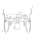
処理ケ−ス20内部のフィルタユニットFとカップ3との間には、前記処理位置にあるウエハWと対向するように、例えばカップ3と対向する面がカップ3の開口部よりも大きい風量制御部をなす整流部材6が設けられている。この整流部材6は、例えば図5(a)に示すように、側部の一方に開口部60が形成された、断面が四角形状の偏平な中空体であって、3枚の側板61(61a,61b,61c)と第1の整流板をなす天板62と第2の整流板をなす底板63とにより形成され、底板63が支持部材64により、対向する2枚の側板61a,61bの内部に形成された図示しないレ−ルに沿って、天板62に対向する第1の位置と、この第1の位置から前記開口部60側に向けて水平な方向(面方向)に移動可能に構成されている。
【0028】
前記天板62と底板63との間は例えば5mm程度に形成され、これら天板62と底板63とには、図5(b)に示すように、フィルタユニットFからの清浄な空気を通気させるための第1の通気孔62aと第2の通気孔63aが夫々形成されている。これら通気孔62a,63bは、天板62及び底板63に同様のパタ−ンで形成されており、このパタ−ンは、例えば図6(a),(b)に天板62と底板63との一部を示すように、移動方向に隣接する通気孔62a(63a)同士の距離L1が、通気孔62a(63a)の移動方向側の最大径L2よりも大きくなるように設定されている。
【0029】
これにより底板63が前記第1の位置にあるときには、図6(a)に示すように、天板62と底板63の通気孔62a,63aが縦方向(面方向に直交する方向)に重なり合うので、この重なった通気孔62a(63a)を介してフィルタユニットFからの空気が下側に通気して行き、こうして清浄化された空気が通気孔62a(63a)の通気により流れの均一性が高められた状態でウエハ保持部2上のウエハWに向かって流れていくことになる。
【0030】
一方、底板63が前記第1の位置の位置から前記開口部60側に向けて僅かに、例えばL2より大きくL1よりも小さな距離分移動した第2の位置にあるときには、図6(b)に示すように、天板62と底板63の通気孔62a,63aが縦方向に重なり合わず、天板62の通気孔62aが下側の底板63で出口側を塞がれた状態になる。従ってこの場合にはフィルタユニットFからの空気は底板63を通過できず、結局整流部材6により気流が遮られた状態になり、整流部材6の側方を下側に向けて通気して行くことになる。
【0031】
続いて上述の装置を用いて行われる本発明方法の一実施の形態を、図7及び図8を用いて説明する。先ず図7(a)に示すように、整流部材6の底板63を前記第1の位置に位置させて、開閉バルブ36を開き、処理ケ−ス20内にフィルタユニットF及び整流部材の通気孔62a,63aを介して、不純物が除去され、所定の温度及び湿度に調整された清浄な空気のダウンフロ−を形成し、風量は0.3m/s程度に調整する。この場合には開閉バルブ36が開いているので、処理ケ−ス20内の雰囲気は排出路35及び排気路23から流出し、これにより処理ケ−ス20内では、カップ3の内側及び外側において風が下方側に流れることになる。
【0032】
この状態で、ウエハ保持部2を前記受け渡し位置まで上昇させ、レジスト膜が形成され露光されたウエハWを、図示しない搬送ア−ムによりウエハ保持部2上に受け渡し、当該ウエハ保持部2に真空吸着させる。ここで処理ケ−ス20内には、既述のようにダウンフロ−が形成されているので、ウエハ保持部2に保持されているウエハWの表面には、上方側から風が流れてくることになる。なおウエハWをウエハ保持部2に押し付ける手法は、例えばウエハWの周縁を機械的に押し付けるメカチャックを用いてもよい。
【0033】
次いで処理ケ−ス20内に風量0.3m/s程度のダウンフロ−を形成したまま、図8(a)に示すように、待機位置にあるノズル4をウエハ保持部2の上方位置を介して供給位置まで移動させて、ノズル4から現像液Dを吐出させ、ウエハWの中心線近傍に現像液Dを供給すると共に、ウエハ保持部2を例えば30rpm程度の回転数で180度回転させて現像液Dの液盛りを行う。つまり処理位置ではノズル4の供給孔42の先端がノズル4からウエハ表面に供給した現像液Dに接触するようになっており、この状態でウエハWを180度回転させながら、供給孔42からウエハ表面に現像液Dを供給すると、回転の遠心力による現像液Dの拡散と、ノズル4の供給孔42による現像液Dの伸展によって、ウエハWの表面全体に現像液Dが塗布され、液盛りが行われる。
【0034】
続いて図7(b)に示すように、ノズル4を待機位置まで移動させ、整流部材6の底板63を前記第2の位置に位置させると共に、開閉バルブ36を閉じ、例えば60秒間ウエハWの回転を停止させて現像を行う。この状態では、開閉バルブ36が閉じられているので、処理ケ−ス20内の雰囲気は排気路23のみから流出する。また整流部材6の底板63が前記第2の位置に位置しているので、既述のようにフィルタユニットFからの空気は整流部材6を通過できずに、整流部材6の側方を下側に向けて通流して行く。これらにより処理ケ−ス20内では、カップ3の外側において風が下方側に流れることになる。
【0035】
このようにして現像を行うが、図9に示すように、現像が終了する直前例えば1秒前に、整流部材6の底板63を前記第1の位置に位置させると共に、開閉バルブ36を開き、処理ケ−ス20内に風量0.3m/s程度のダウンフロ−を形成する。そして図8(c)に示すように、待機位置にあるリンス用ノズル45をウエハ保持部2の上方位置を介して供給位置まで移動させ、ウエハ保持部2を回転させながらリンス用ノズル45からリンス液Rを吐出させて洗浄を行う。次いで処理ケ−ス20内に風量0.3m/s程度のダウンフロ−を形成した状態で、図8(d)に示すように、ウエハWを高速で回転させることによりウエハ表面を乾燥させ、この後ウエハ保持部2をウエハWの受け渡し位置まで上昇させてウエハWを図示しない搬送ア−ムに受け渡す。
【0036】
ここでウエハ保持部2へのウエハWの受け渡しや、ノズル4やリンス用ノズル45のウエハ上方部への移動の際には、外カップ31の上端を前記ウエハWの受け渡し位置よりも下方側に位置させ、ウエハWへの現像液Dやリンス液Rの供給時や現像時、乾燥時には、外カップ31の上端を前記ウエハWの受け渡し位置よりも上方側に位置させて所定の処理を行う。
【0037】
このような現像方法では、現像時には、処理ケ−ス20内のダウンフロ−の気流を整流部材6によりウエハ上方側にて遮り、ウエハ表面へ風が流れないようにしているので、ウエハ表面に現像液Dの温度分布が発生しにくく、均一性の高い現像処理を行うことができる。
【0038】
つまり現像時には処理ケ−ス20内においては、上方からウエハWに当たる風がほとんど無いか、極めて少ない状態になっているので、ウエハ面に沿って外方側へ流れる風量も極めて少ない。このためウエハWの中央近傍領域に比べて周縁領域の方が風量が多くなるといったことが発生しにくいので、ウエハWの周縁領域における気化熱が大きくなるということが生じにくい。これによりウエハWの面内において現像液Dの放熱量がほぼ同じ状態となるので、結果としてウエハ上の現像液Dの温度低下の程度が面内おいてほぼ揃えられる。
【0039】
このため現像液Dの温度がウエハ面内に亘ってほぼ均一な状態で現像が行われるので、温度差が原因となる現像ムラの発生が抑制され、これにより現像線幅の寸法の変化が抑えられて、現像処理の均一性が高められる。実際にI線レジストが塗布され、所定のパタ−ン形状に露光されたウエハWに対して上述の現像装置にて現像処理を行ったところ、ウエハWの中央近傍領域と周縁領域ろの間で現像線幅の狂いはほとんどなく、均一な現像処理を行うことができることが認められた。
【0040】
また上述の例では、現像時においても、カップ3の外側ではダウンフロ−が形成されているので、処理ケ−ス20内の陽圧化が図れると共に、駆動系からのパ−ティクルの浮遊を抑えることができる。さらに上述の例では、現像が終了する直前に処理ケ−ス20内にダウンフロ−を形成しているが、これはリンス処理によりカップ外へミストが飛散するのを防止するためである。
【0041】
以上において本発明では、現像時にウエハWへの風が当たる領域を調整することにより現像処理の均一性を高めるようにしてもよい。つまり例えば現像時にはウエハWの中央近傍領域の風量を周縁領域よりも多くしてもよいし、例えば現像時にはウエハWの中央近傍領域のみに風が当たり、周縁領域には風が当たらないようにしてもよい。
【0042】
この際ウエハWへの風量は、他の条件が同じ場合には、整流部材の通気孔62a(63a)の大きさにより調整でき、通気孔62a(63a)が大きければ風量が多くなる。従って底板63を第2の位置にスライドさせたときに、天板62のウエハWの中央近傍領域に対応する位置の通気孔62aが、ウエハWの周縁領域に対応する位置の通気孔62aよりも大きくなるように、天板62の通気孔62aを底板63の通気孔63aが形成されていない部分で縦方向に塞ぐようにすれば、ウエハWの中央近傍領域の風量が周縁領域よりも多くなる。
【0043】
また底板63を第2の位置にスライドさせたときに、天板62のウエハWの中央近傍領域に対応する位置の通気孔62aは開いた状態とし、ウエハWの周縁領域に対応する位置の通気孔62aは閉じた状態になるように、天板62の通気孔62aを底板63の通気孔63aが形成されていない部分で縦方向に塞ぐようにすれば、ウエハWの中央近傍領域のみに風が当たるようになる。
【0044】
このように現像時にはウエハWの中央近傍領域の風量を外周部よりも多くしたり、現像時にはウエハWの中央近傍領域のみに風が当たるようにしても、ウエハWに上から当たった風はウエハ面を外方側に流れていき、これによりウエハWの周縁領域の風量が多くなるので、ウエハWの面内において風量がほぼ揃えられた状態となり、ウエハ面内における現像液の温度分布の発生を抑えて、均一性の高い現像処理を行うことができる。
【0045】
上述実施の形態において、乱流が形成されることを防止する観点から、静止現像時以外(図7(a)参照)は、フィルタユニットFから下方に向けて噴出される空気の量が、排出路35及び排気路23から排気される空気の風量と一致するようにフィルタユニットFの風量を調整し、静止現像時(図7(b)参照)は、フィルタユニットFから下方に向けて噴出される空気の量が、排気路23から排気される空気の風量と一致するようにフィルタユニットFの風量を調整することが好ましい。但し、静止現像に入る直前、即ち排出路35を閉じる直前にはフィルタユニットFの風量を通常よりも増量するように調整することが好ましい。
【0046】
また上述実施の形態では、図7(b)に示すように、静止現像時には開閉バルブ36を閉じ、処理ケース20内の雰囲気は排気路23のみから流出するようにしていたが、図10に示すように、処理ケース20の側部であってカップ3よりも上方側に排気路123を別に設け、静止現像時には開閉バルブ36,排気路23を閉じて排気路123のみから雰囲気が流出するように構成してもよい。このように構成すると、静止現像時にダウンフローの空気が直接ウエハWに当たることをより確実に防止することができる。
【0047】
また図1に示すように、処理ケース20の側部の、整流部材6の天板62より上部には、整流部材6で側方に流れ込む空気を処理ケース20の外側に逃がすための排気孔120を設けることが好ましい。これにより、整流部材6で側方に流れ込んだ空気により処理ケース20内に乱流が発生することを抑えることができる。また排気孔120を送出路52に接続するようにすれば、清浄空気の有効利用を図ることができる。
【0048】
次に本発明に係る現像方法の実施に使用される現像装置をユニットに組み込んだ塗布・現像装置の一例の概略について図11及び図12を参照しながら説明する。図11及び図12中、7はウエハカセットを搬入出するための搬入出ステ−ジであり、例えば25枚収納されたカセットCが例えば自動搬送ロボットにより載置される。搬入出ステ−ジ7に臨む領域にはウエハWの受け渡しア−ム70が,X,Y方向及びθ回転(円鉛直軸回りの回転)自在に設けられている。更にこの受け渡しア−ム70の奥側には、例えば搬入出ステ−ジ7から奥を見て例えば右側には塗布・現像系のユニットU1が、左側、手前側、奥側には加熱・冷却系のユニットU2,U3,U4が夫々配置されていると共に、塗布・現像系ユニットと加熱・冷却系ユニットとの間でウエハWの受け渡しを行うための、例えば昇降自在、左右、前後に移動自在かつ鉛直軸まわりに回転自在に構成されたウエハ搬送ア−ムMAが設けられている。但し図11では便宜上ユニットU2及びウエハ搬送ア−ムMAは描いていない。
【0049】
塗布・現像系のユニットにおいては、例えば上段に2個の現像ユニット71が、下段に2個の塗布ユニット72が設けられている。加熱・冷却系のユニットにおいては、加熱ユニットや冷却ユニットや疎水化処理ユニット等が上下にある。前記塗布・現像系ユニットや加熱・冷却系ユニットを含む上述の部分をクリ−ントラックと呼ぶことにすると、このクリ−ントラックの奥側にはインタ−フェイスユニット72を介して露光装置73が接続されている。インタ−フェイスユニット72は、例えば昇降自在、左右、前後に移動自在かつ鉛直軸まわりに回転自在に構成されたウエハ搬送ア−ム74によりクリ−ントラックと露光装置73との間でウエハWの受け渡しを行うものである。
【0050】
この装置のウエハの流れについて説明すると、先ず外部からウエハWが収納されたウエハカセットCが前記搬入出ステ−ジ7に搬入され、ウエハ搬送ア−ム70によりカセットC内からウエハWが取り出され、既述の加熱・冷却ユニットU3の棚の一つである受け渡し台を介してウエハ搬送ア−ムMAに受け渡される。次いでユニットU3内の一の棚の処理部内にて疎水化処理が行われた後、塗布ユニット72にてレジスト液が塗布され、レジスト膜が形成される。レジスト膜が塗布されたウエハWは加熱ユニットで加熱された後インタ−フェイスユニット72を介して露光装置73に送られ、ここでパタ−ンに対応するマスクを介して露光が行われる。
【0051】
その後ウエハWは加熱ユニットで加熱された後、冷却ユニットで冷却され、続いて現像ユニット71に送られて現像処理され、レジストマスクが形成される。しかる後ウエハWは搬入出ステ−ジ7上のカセットC内に戻される。
【0052】
以上において本発明では、基板としてはウエハに限らず、液晶ディスプレイ用のガラス基板であってもよい。また整流部材6の天板62と底板63とは相対的に横方向にスライドさせるように構成すればよく、どちらを移動させるようにしてもよい。
【0053】
さらに整流部材6は、現像時にウエハ表面への気流を遮るものであれば、形状や取り付け位置等は上述の構成に限るものではない。例えば図13に示すように、整流部材136の天板162と底板163とは相対的に回転させるように構成してもよい。
【0054】
また図14に示すように、整流部材146として、長尺の板状部材147を、長さ方向に略直交する方向に多数並べて、例えばウエハWを覆う大きさの矩形を形成し、各板状部材147を夫々別個の回転駆動部をなす回転駆動機構148により、板状部材147の長手方向の一辺に設けられた図示しない回転軸を介して水平軸回りに回転させ、これによりウエハWに対して空気を通気させるための開口を形成することで気流の遮蔽量を調整するようにしてもよい。このような構成では、各板状部材147は夫々別個の回転駆動機構148で駆動されるので、整流部材146上の各領域に応じて気流の遮蔽量を変えることができる。また板状部材147の回転角度を調整し、開口の程度を変えることで気流の遮蔽量を調整するようにしてもよい。
【0055】
また図15に示すように、各板状部材147を回転駆動部をなす回転駆動機構152に接続された連結部材151で連結し、例えばこの連結部材の151の内部において各板状部材147の回転軸を歯車等を介して連結しておき、回転駆動機構152により各板状部材147を同時に一括して回転駆動するようにしてもよい。この例では1つの回転駆動機構152により各板状部材147を回転駆動しているので、駆動機構152の部品点数を減らすことができる。この際駆動機構152を図中矢印で示すように連結部材151に沿って各板状部材147に対応する位置まで移動させて、この位置の板状部材147の図示しない回転軸を介して、当該板状部材147を駆動機構152により個別に水平軸回りに回転させるように構成してもよい。
【0056】
さらに図16に示すように、例えば整流部材166の天板172に設けられた第1の通気孔162a及び底板173に設けられた第2の通気孔163aの密度を整流部材166上の領域に応じて変えることで、各領域毎に気流の遮蔽量を調整することができる。図に示す例は整流部材166の中央側において、周縁側よりも第1の通気孔162a,第2の通気孔163aの密度を高めた例であり、このようにすると、ウエハWの周縁領域よりも中央近傍領域側の通気用の開口が大きくなるので、ウエハW表面の中央近傍領域に当たる風の風量を周縁領域よりも多くすることができる。
【0057】
さらにまた図17に示すように、整流部材176の底板173をその中央から折り曲げ可能とし、このように中央から両側が下側を向くように折り曲げるようにしてもよい。このような構成では、天板62と底板173とにほぼ同じ間隔でほぼ同じ大きさの通気孔62a,63aが形成されており、中央部の通気孔62a,63a同士が重なるようにして、底板173の両側を下側に折り曲げた場合には、天板62と底板173とが離れるに連れて、通気孔62a,63aの重なりも少なくなるので、結果としてウエハWの周縁領域よりも中央近傍領域側の通気用の開口が大きくなり、これによりウエハW表面の中央近傍領域に当たる風の風量を周縁領域よりも多くすることができる。
【0058】
さらにまた本発明は、ウエハWを例えば10rpm程度の回転数で低速で回転させながら現像を行っても良いし、ウエハWに現像液を供給するためのノズルは上述の例に限るものではなく、ウエハWの中央近傍に現像液を供給した後、ウエハWを回転させて、回転の遠心力により現像液をウエハ表面全体に伸展させるタイプのものであってもよい。
【0059】
【発明の効果】
本発明によれば、現像液の基板の面内の温度変化の程度が揃えられ、基板面内の現像液の温度の均一性が高まるので、現像液の温度差が原因となる処理ムラの発生が抑えられ、均一性の高い処理を行うことができる。
【図面の簡単な説明】
【図1】本発明の実施の形態に係る現像装置の一例の全体構成を示す断面図である。
【図2】前記現像装置で用いられるウエハ保持部を示す断面図である。
【図3】前記現像装置で用いられるノズルを示す斜視図と底面図である。
【図4】前記現像装置を示す平面図である。
【図5】前記現像装置で用いられる整流部材を示す斜視図と平面図である。
【図6】前記現像装置で用いられる整流部材を示す平面図と断面図である。
【図7】前記現像装置の作用を示す断面図である。
【図8】前記現像装置の作用を示す断面図である。
【図9】ウエハ表面への風量と時間との関係を示す特性図である。
【図10】本発明の他の実施の形態に係る現像装置を示す断面図である。
【図11】前記現像装置を組み込んだ塗布・現像装置の一例を示す斜視図である。
【図12】前記現像装置を組み込んだ塗布・現像装置の一例を示す平面図である。
【図13】整流部材の他の例を示す斜視図である。
【図14】整流部材のさらに他の例を示す斜視図である。
【図15】整流部材のさらに他の例を示す斜視図である。
【図16】整流部材のさらに他の例を示す斜視図である。
【図17】整流部材のさらに他の例を示す斜視図である。
【図18】従来の現像方法を説明するための断面図である。
【図19】従来の現像装置を示す断面図である。
【図20】従来の現像装置におけるウエハ面の風の流れを説明するための断面図である。
【符号の説明】
2 ウエハ保持部
3 カップ
31 外カップ
32 内カップ
4 ノズル
6 整流部材
W 半導体ウエハ
D 現像液
F フィルタユニット[0001]
BACKGROUND OF THE INVENTION
The present invention relates to a developing apparatus and a method for performing substrate processing such as development processing on a substrate.
[0002]
[Prior art]
A mask for forming a predetermined pattern on the surface of a semiconductor wafer (hereinafter referred to as “wafer”) or a glass substrate (LCD substrate) of a liquid crystal display is obtained by applying a resist to the surface of a substrate such as a wafer, It is obtained by irradiating the resist surface with a line or ion beam and developing it. Here, the development processing is performed by dissolving a portion irradiated with light or the like in the exposure step or a portion not irradiated with an alkaline aqueous solution or the like, and is conventionally performed by the method shown in FIG.
[0003]
That is, in this conventional method, a substrate, for example, a wafer W is sucked and held on a
[0004]
As a result, the
[0005]
Here, a conventional developing apparatus in which such development processing is performed will be briefly described with reference to FIG. 19. The periphery of the
[0006]
An
[0007]
[Problems to be solved by the invention]
However, for example, when an I-line resist is used, development unevenness occurs in the development method described above, and the development line width changes depending on the part. For example, the line width is about 4 nm between the wafer central region and the peripheral region. There is a problem that it ends up. Examining this cause, the degree of progress of development depends on the temperature of the
[0008]
That is, the
[0009]
For this reason, at the start of rinsing, a temperature difference of the developing
[0010]
The present invention has been made under such circumstances. The object of the present invention is to suppress the development unevenness due to the temperature difference of the developer by making the temperature of the developer substantially uniform in the plane of the substrate during development. Thus, it is an object of the present invention to provide a developing apparatus and method for improving processing uniformity.
[0011]
[Means for Solving the Problems]
For this reason, the developing device of the present invention is a substrate for holding the substrate in a developing device that performs development by depositing a developer on the surface of the substrate in an atmosphere in which an airflow directed toward the surface of the substrate is formed. A holding portion, a supply portion for supplying a developing solution to the substrate, and a first ventilation hole provided on the surface side of the substrate held by the substrate holding portion so as to face the substrate and having a first vent hole formed therein The second rectifying plate is provided so as to face the first rectifying plate so that the rectifying plate can be moved relative to the first rectifying plate relative to the first rectifying plate. A baffle plate, While a developer is supplied to the held substrate and development of the substrate is performed, The first rectifying plate and the second rectifying plate are relatively moved in the surface direction so that the first vent hole and the region where the second vent hole of the second rectifying plate is not formed are faced. Adjust the size of the first vent by overlapping in the direction orthogonal to the direction, The size of the first ventilation hole is made larger in the vicinity of the center area than the peripheral area of the substrate, and the amount of wind hitting the vicinity of the center area of the substrate surface is made larger than that in the peripheral area. It is characterized by that.
[0012]
In such a developing device, since the amount of wind striking the substrate surface can be controlled, the heat of vaporization of the developer on the substrate, which changes according to the amount of air blown to the substrate surface, can be adjusted, resulting in development on the substrate. The temperature of the liquid can be controlled.
[0013]
Specifically, when developing the surface of the substrate with the first vent hole kept in a state where the developer is accumulated on the substrate, it is more than when the developer is accumulated on the substrate surface. The amount of wind that strikes the substrate surface is reduced during the development than when the developer is deposited, and in this case, it is also included that the substrate surface is not exposed to wind during development. It is. In other words, in this developing device, in the atmosphere in which an airflow directed toward the surface of the substrate is formed, the step of depositing the developer on the surface of the substrate, and then the state in which the developer is accumulated on the substrate, And developing the substrate surface while preventing the surface from being exposed to wind.
[0014]
Thus, if the wind is not applied to the substrate surface during development, the change in the heat of vaporization of the developer on the substrate due to the influence of the wind is suppressed, and the heat radiation amount of the developer becomes substantially uniform in the plane of the substrate. For this reason, the temperature changes of the developer on the substrate are substantially uniform in the plane of the substrate, and the occurrence of uneven development due to the temperature difference of the developer is suppressed, and the processing uniformity can be improved.
[0015]
Further, in the present invention, the substrate surface may be developed while adjusting the area where the wind is applied to the substrate surface. For example, when developing the substrate surface, the size of the first vent is set to You may make it the center vicinity area | region side larger than a periphery area | region, and may make it the air volume of the wind which hits the center vicinity area | region of a board | substrate surface more than a periphery area | region. Here, the case where the wind hits only the region near the center of the substrate and the wind does not hit the peripheral region is included.
[0016]
Even in this case, the wind that hits the substrate flows toward the peripheral area along the surface of the substrate, and when the air uniformly hits the entire surface of the substrate, the air volume is larger in the peripheral area. By making the air volume hitting the area near the center of the substrate surface larger than that in the peripheral area, as a result, the air volume hitting the board becomes almost uniform in the plane of the substrate. For this reason, since the temperature change of the developing solution on the substrate is almost uniform in the plane of the substrate, the uniformity of the developing process can be improved.
[0017]
DETAILED DESCRIPTION OF THE INVENTION
FIG. 1 is a longitudinal sectional view showing an overall configuration of an embodiment of a developing device when the present invention is applied to the developing device, in which 20 is a processing chamber for housing the developing device. (Development processing room) In the
[0018]
The wafer holding unit 2 will be described with reference to FIG. 2. The wafer holding unit 2 has, for example, a vacuum suction function, and is driven around a vertical axis via a rotating
[0019]
The periphery of the wafer holding unit 2 surrounds the periphery of the wafer W at the processing position, and when the developer supplied on the wafer is shaken off, the liquid is prevented from splashing around. A circular
[0020]
The inner cup 32 is provided on the inner side of the
[0021]
Above the wafer W at the processing position vacuum-sucked by the wafer holding unit 2, a processing liquid, for example, a developer is supplied to the surface of the wafer W. Developer A
[0022]
For example, as shown in FIG. 4, the
[0023]
Such a
[0024]
Further, on the upper side of the
[0025]
On the other hand, a gas-liquid separation means 5 to which the other end of the
[0026]
The
[0027]
Between the filter unit F in the
[0028]
The space between the
[0029]
As a result, when the
[0030]
On the other hand, when the
[0031]
Subsequently, an embodiment of the method of the present invention performed using the above-described apparatus will be described with reference to FIGS. First, as shown in FIG. 7A, the
[0032]
In this state, the wafer holder 2 is raised to the delivery position, and the wafer W formed with the resist film and exposed is delivered onto the wafer holder 2 by a transfer arm (not shown), and the wafer holder 2 is vacuumed. Adsorb. Here, since the down flow is formed in the
[0033]
Next, with the down flow having a flow rate of about 0.3 m / s formed in the
[0034]
Subsequently, as shown in FIG. 7B, the
[0035]
In this way, as shown in FIG. 9, as shown in FIG. 9, the
[0036]
Here, when the wafer W is transferred to the wafer holding unit 2 or when the
[0037]
In such a development method, during development, the downflow airflow in the
[0038]
In other words, since there is almost no wind hitting the wafer W from above or very little in the
[0039]
For this reason, the development is performed in a state where the temperature of the developer D is substantially uniform over the wafer surface, so that the development unevenness caused by the temperature difference is suppressed, thereby suppressing the change in the dimension of the development line width. As a result, the uniformity of the development process is improved. When the developing process is performed on the wafer W that is actually coated with an I-line resist and exposed to a predetermined pattern shape, the wafer W is located between the central region and the peripheral region of the wafer W. It was recognized that there was almost no deviation in the development line width and that uniform development processing could be performed.
[0040]
In the above-described example, even during development, a downflow is formed outside the
[0041]
As described above, in the present invention, the uniformity of the development process may be improved by adjusting the area where the wind is applied to the wafer W during development. That is, for example, the air volume in the vicinity of the center of the wafer W may be larger than that in the peripheral area at the time of development. For example, the wind may be applied only to the area near the center of the wafer W during development. Also good.
[0042]
At this time, the air volume to the wafer W can be adjusted by the size of the
[0043]
When the
[0044]
As described above, even when the air volume in the vicinity of the center of the wafer W is larger than that of the outer periphery during development, or the wind is applied only to the vicinity of the center of the wafer W during development, Since the airflow in the peripheral area of the wafer W increases as the surface flows outward, the airflow is almost uniform in the surface of the wafer W, and the temperature distribution of the developer in the wafer surface is generated. And development processing with high uniformity can be performed.
[0045]
In the above-described embodiment, from the viewpoint of preventing the formation of turbulent flow, the amount of air ejected downward from the filter unit F is discharged except during static development (see FIG. 7A). The air volume of the filter unit F is adjusted so that it matches the air volume of the air exhausted from the
[0046]
In the above-described embodiment, as shown in FIG. 7B, the open /
[0047]
Further, as shown in FIG. 1, on the side of the
[0048]
Next, an outline of an example of a coating / developing apparatus in which a developing apparatus used for carrying out the developing method according to the present invention is incorporated in a unit will be described with reference to FIGS. In FIGS. 11 and 12,
[0049]
In the coating / developing unit, for example, two developing
[0050]
The flow of wafers in this apparatus will be described. First, the wafer cassette C in which the wafers W are stored from the outside is loaded into the loading /
[0051]
Thereafter, the wafer W is heated by the heating unit, then cooled by the cooling unit, and subsequently sent to the developing
[0052]
In the present invention, the substrate is not limited to a wafer, but may be a glass substrate for a liquid crystal display. Further, the
[0053]
Furthermore, as long as the rectifying
[0054]
As shown in FIG. 14, as the rectifying
[0055]
Further, as shown in FIG. 15, each plate-
[0056]
Further, as shown in FIG. 16, for example, the density of the first ventilation holes 162 a provided on the
[0057]
Furthermore, as shown in FIG. 17, the
[0058]
Furthermore, the present invention may perform development while rotating the wafer W at a low speed of, for example, about 10 rpm, and the nozzle for supplying the developer to the wafer W is not limited to the above example. After the developer is supplied to the vicinity of the center of the wafer W, the wafer W may be rotated, and the developer may be extended over the entire wafer surface by the centrifugal force of rotation.
[0059]
【The invention's effect】
According to the present invention, the degree of temperature change in the surface of the substrate of the developing solution is made uniform, and the uniformity of the temperature of the developing solution in the substrate surface is increased, so that processing unevenness caused by the temperature difference of the developing solution occurs. Can be suppressed, and highly uniform processing can be performed.
[Brief description of the drawings]
FIG. 1 is a cross-sectional view showing an overall configuration of an example of a developing device according to an embodiment of the present invention.
FIG. 2 is a cross-sectional view showing a wafer holder used in the developing device.
FIG. 3 is a perspective view and a bottom view showing a nozzle used in the developing device.
FIG. 4 is a plan view showing the developing device.
FIGS. 5A and 5B are a perspective view and a plan view showing a rectifying member used in the developing device. FIGS.
6A and 6B are a plan view and a cross-sectional view showing a rectifying member used in the developing device.
FIG. 7 is a cross-sectional view showing the operation of the developing device.
FIG. 8 is a cross-sectional view showing the operation of the developing device.
FIG. 9 is a characteristic diagram showing the relationship between the air volume to the wafer surface and time.
FIG. 10 is a cross-sectional view showing a developing device according to another embodiment of the present invention.
FIG. 11 is a perspective view showing an example of a coating / developing apparatus incorporating the developing device.
FIG. 12 is a plan view showing an example of a coating / developing apparatus incorporating the developing device.
FIG. 13 is a perspective view showing another example of the rectifying member.
FIG. 14 is a perspective view showing still another example of the rectifying member.
FIG. 15 is a perspective view showing still another example of the rectifying member.
FIG. 16 is a perspective view showing still another example of the rectifying member.
FIG. 17 is a perspective view showing still another example of the rectifying member.
FIG. 18 is a cross-sectional view for explaining a conventional developing method.
FIG. 19 is a cross-sectional view showing a conventional developing device.
FIG. 20 is a cross-sectional view for explaining the flow of air on the wafer surface in a conventional developing device.
[Explanation of symbols]
2 Wafer holder
3 cups
31 outer cup
32 inner cups
4 nozzles
6 Rectification member
W Semiconductor wafer
D Developer
F Filter unit
Claims (12)
前記基板を保持するための基板保持部と、
基板に現像液を供給するための供給部と、
前記基板保持部に保持された基板の表面側に、基板と対向するように設けられ、第1の通気孔が形成された第1の整流板と、
前記第1の整流板と相対的に面方向に移動できるように、この第1の整流板と対向するように設けられ、第2の通気孔が形成された第2の整流板と、を備え、 前記保持された基板に現像液が供給され、前記基板の現像が行われる間に、前記第1の整流板と第2の整流板とを相対的に面方向に移動させ、第1の通気孔と、第2の整流板の第2の通気孔が形成されていない領域とを面方向に直交する方向に重ねることにより第1の通気孔の大きさを調整し、前記第1の通気孔の大きさを基板の周縁領域よりも中央近傍領域側を大きくし、基板表面の中央近傍領域に当たる風の風量を周縁領域よりも多くすることを特徴とする現像装置。In a developing device that performs development by depositing a developer on the surface of the substrate in an atmosphere in which an airflow toward the surface of the substrate is formed,
A substrate holding part for holding the substrate;
A supply unit for supplying a developer to the substrate;
A first baffle plate provided on the front surface side of the substrate held by the substrate holding portion so as to face the substrate and having a first vent hole;
A second rectifying plate provided so as to face the first rectifying plate and formed with a second air hole so that the first rectifying plate can be moved in a plane direction relative to the first rectifying plate. While the developer is supplied to the held substrate and the development of the substrate is performed, the first rectifying plate and the second rectifying plate are moved relative to each other in the plane direction, and the first passage The size of the first air hole is adjusted by overlapping the air hole and a region where the second air hole of the second current plate is not formed in a direction perpendicular to the surface direction, and the first air hole The developing device is characterized in that the size of is larger in the region near the center than in the peripheral region of the substrate, and the amount of wind hitting the region near the center of the substrate surface is larger than that in the peripheral region .
前記基板保持部により保持された基板の被処理面に処理液を供給するための液供給部と、
前記基板保持部に保持された基板の被処理面側から、前記基板保持部及びその周囲に向けて気体を供給するための気体供給部と、
前記基板保持部と前記気体供給部との間に設けられ、前記気体供給部から供給される気体を遮蔽することにより、基板表面に当たる風の風量を制御する風量制御部と、を備え、
前記風量制御部は、前記基板と対向するように、長さ方向と略直交する方向に配列され、長さ方向の一辺に沿って略垂直方向に回転可能な複数の板状部材と、前記各板状部材を回転させる回転駆動部と、を含み、前記板状部材を回転させて開口部を形成し、この開口部の大きさを調整することにより、基板表面に当たる風の風量を制御することを特徴とする基板処理装置。 A substrate holder for holding the substrate;
A liquid supply unit for supplying a processing liquid to the surface to be processed of the substrate held by the substrate holding unit;
A gas supply unit for supplying gas toward the substrate holding unit and the periphery thereof from the surface to be processed of the substrate held by the substrate holding unit;
An air volume control unit that is provided between the substrate holding unit and the gas supply unit and controls the air volume of the wind that hits the substrate surface by shielding the gas supplied from the gas supply unit ;
The air volume control unit is arranged in a direction substantially orthogonal to the length direction so as to face the substrate, and a plurality of plate-like members that are rotatable in a substantially vertical direction along one side in the length direction; A rotation drive unit that rotates the plate-shaped member, and the plate-shaped member is rotated to form an opening, and the size of the opening is adjusted to control the amount of air hitting the substrate surface. A substrate processing apparatus.
前記処理室内に設けられ、上部に開口を有するカップと、
前記カップ内に設けられ、基板を保持するための基板保持部と、
前記基板保持部により保持された基板の被処理面に処理液を供給するための液供給部と、
前記処理室の上部側に設けられ、前記処理室の下方側に向けて気体を供給するための気体供給部と、
前記基板保持部と前記気体供給部との間に設けられ、前記気体供給部から供給される気体を遮蔽することにより、基板表面に当たる風の風量を制御する風量制御部と、
前記処理室の下部側に設けられ、この処理室から気体を排気する第1の気体排気部と、
前記カップの下部側に設けられ、このカップから気体を排気する第2の気体排気部と、を備え、
前記風量制御部は、前記基板と対向するように、長さ方向と略直交する方向に配列され、長さ方向の一辺に沿って略垂直方向に回転可能な複数の板状部材と、前記各板状部材を回転させる回転駆動部と、を含み、前記板状部材を回転させて開口部を形成し、この開口部の大きさを調整することにより、基板表面に当たる風の風量を制御することを特徴とする基板処理装置。 A processing chamber;
A cup provided in the processing chamber and having an opening at the top;
A substrate holding part provided in the cup for holding the substrate;
A liquid supply unit for supplying a processing liquid to the surface to be processed of the substrate held by the substrate holding unit;
A gas supply section provided on the upper side of the processing chamber, for supplying gas toward the lower side of the processing chamber;
An air volume control unit that is provided between the substrate holding unit and the gas supply unit, and controls the air volume of the wind that hits the substrate surface by shielding the gas supplied from the gas supply unit;
A first gas exhaust unit provided on the lower side of the processing chamber and exhausting gas from the processing chamber;
A second gas exhaust part provided on the lower side of the cup and exhausting gas from the cup ;
The air volume control unit is arranged in a direction substantially orthogonal to the length direction so as to face the substrate, and a plurality of plate-like members that are rotatable in a substantially vertical direction along one side in the length direction; A rotation drive unit that rotates the plate-shaped member, and the plate-shaped member is rotated to form an opening, and the size of the opening is adjusted to control the amount of air hitting the substrate surface. A substrate processing apparatus.
前記連結部材を介して前記各板状部材を一括して回転させる回転駆動機構と、を備えることを特徴とする請求項4又は5記載の基板処理装置。The rotation driving unit includes a connecting member that connects the plate-like members in a direction substantially orthogonal to the length direction;
The substrate processing apparatus according to claim 4 , further comprising: a rotation drive mechanism that rotates the plate-like members collectively through the connecting member.
前記現像処理室内に設けられ、上部に開口を有するカップと、A cup provided in the development processing chamber and having an opening at the top;
前記カップ内に設けられ、基板を保持するための基板保持部と、A substrate holding part provided in the cup for holding the substrate;
前記基板保持部により保持された基板の被処理面に現像液を供給するための現像液供給部と、A developer supply unit for supplying a developer to the processing surface of the substrate held by the substrate holding unit;
前記現像処理室の上部側に設けられ、前記現像処理室の下方側に向けて気体を供給するための気体供給部と、A gas supply unit provided on the upper side of the development processing chamber, for supplying gas toward the lower side of the development processing chamber;
前記基板保持部と前記気体供給部との間に設けられ、前記気体供給部から供給される気体を遮蔽することにより、基板表面に当たる風の風量を制御する風量制御部と、An air volume control unit that is provided between the substrate holding unit and the gas supply unit, and controls the air volume of the wind hitting the substrate surface by shielding the gas supplied from the gas supply unit;
前記現像処理室の下部側に設けられ、この現像処理室から気体を排気する第1の気体排気部と、A first gas exhaust unit provided on the lower side of the development processing chamber for exhausting gas from the development processing chamber;
前記カップの下部側に設けられ、このカップから気体を排気する第2の気体排気部と、を備え、A second gas exhaust part provided on the lower side of the cup and exhausting gas from the cup;
前記風量調整部は、前記基板と対向するように設けられ、第1の通気孔が形成された第1の整流板と、The air volume adjusting unit is provided so as to face the substrate, and a first rectifying plate in which a first air hole is formed;
前記第1の整流板と相対的に面方向に移動でき、かつ前記第1の整流板と対向するように構成されて第2の通気孔が形成された第2の整流板と、を含み、A second rectifying plate that is movable in a plane direction relative to the first rectifying plate and is configured to face the first rectifying plate and has a second air hole formed therein,
前記第1の整流板の第1の通気孔と第2の整流板の第2の通気孔が形成されていない領域を面方向に直交する方向に重ねることにより、第1の通気孔を塞ぐか又は第1の通気孔の大きさを調整して基板表面に当たる風の風量を制御し、Whether the first vent hole is blocked by overlapping the first vent hole of the first rectifying plate and the region where the second vent hole of the second rectifying plate is not formed in a direction orthogonal to the surface direction. Alternatively, by adjusting the size of the first vent hole to control the air volume hitting the substrate surface,
前記基板に前記現像液が供給される前に、前記第1の気体排気部と前記第2の気体排気部とから気体を排気し、Before the developer is supplied to the substrate, the gas is exhausted from the first gas exhaust unit and the second gas exhaust unit,
前記基板の現像中は、第2の気体排気部からの排気を停止すると共に、前記第1の通気孔を第2の整流板の第2の通気孔が形成されていない領域で塞ぐことにより、前記現像液処理室内に供給される気体が前記カップの外側を通るように調整することを特徴とする現像装置。During the development of the substrate, the exhaust from the second gas exhaust unit is stopped, and the first vent hole is closed in a region where the second vent hole of the second rectifying plate is not formed. A developing device, wherein the gas supplied into the developer processing chamber is adjusted so as to pass outside the cup.
その後基板上に現像液を液盛りした状態のままにして、基板表面への風が当たる領域を調整しながら基板表面を現像する工程と、 Then, the step of developing the substrate surface while adjusting the region where the wind hits the substrate surface while leaving the developer on the substrate,
基板表面を現像する工程は、前記基板保持部と前記気体供給部との間に設けられた風量制御部により、前記気体供給部から供給される気体を遮蔽することにより、基板表面に当たる風の風量を、周縁領域よりも中央近傍領域側を多くしながら行うことを特徴とする現像方法。 The step of developing the substrate surface includes: A developing method characterized in that the step is performed while increasing the area near the center rather than the peripheral area.
Priority Applications (1)
| Application Number | Priority Date | Filing Date | Title |
|---|---|---|---|
| JP2000242808A JP3679695B2 (en) | 1999-08-12 | 2000-08-10 | Developing apparatus, substrate processing apparatus, and developing method |
Applications Claiming Priority (3)
| Application Number | Priority Date | Filing Date | Title |
|---|---|---|---|
| JP11-228671 | 1999-08-12 | ||
| JP22867199 | 1999-08-12 | ||
| JP2000242808A JP3679695B2 (en) | 1999-08-12 | 2000-08-10 | Developing apparatus, substrate processing apparatus, and developing method |
Publications (2)
| Publication Number | Publication Date |
|---|---|
| JP2001118790A JP2001118790A (en) | 2001-04-27 |
| JP3679695B2 true JP3679695B2 (en) | 2005-08-03 |
Family
ID=26528390
Family Applications (1)
| Application Number | Title | Priority Date | Filing Date |
|---|---|---|---|
| JP2000242808A Expired - Fee Related JP3679695B2 (en) | 1999-08-12 | 2000-08-10 | Developing apparatus, substrate processing apparatus, and developing method |
Country Status (1)
| Country | Link |
|---|---|
| JP (1) | JP3679695B2 (en) |
Cited By (1)
| Publication number | Priority date | Publication date | Assignee | Title |
|---|---|---|---|---|
| KR101388593B1 (en) * | 2006-09-27 | 2014-04-23 | 엘아이지에이디피 주식회사 | Apparatus for vapor deposition of organic and method for deposition using the same |
Families Citing this family (9)
| Publication number | Priority date | Publication date | Assignee | Title |
|---|---|---|---|---|
| JP4789352B2 (en) * | 2001-06-19 | 2011-10-12 | キヤノン株式会社 | Exposure apparatus and device manufacturing method |
| US7077585B2 (en) | 2002-07-22 | 2006-07-18 | Yoshitake Ito | Developing method and apparatus for performing development processing properly and a solution processing method enabling enhanced uniformity in the processing |
| FR2869159B1 (en) | 2004-04-16 | 2006-06-16 | Rhodia Chimie Sa | ELECTROLUMINESCENT DIODE EMITTING A WHITE LIGHT |
| JP2008060294A (en) * | 2006-08-31 | 2008-03-13 | Hitachi High-Technologies Corp | Device and method for treating substrate, and manufacturing method for substrate |
| JP6554414B2 (en) * | 2015-12-25 | 2019-07-31 | 株式会社Screenホールディングス | Substrate processing equipment |
| KR102387542B1 (en) * | 2017-05-11 | 2022-04-19 | 주식회사 케이씨텍 | Air supply system and apparatus for treating substrate |
| CN114144733A (en) * | 2019-07-31 | 2022-03-04 | 东京毅力科创株式会社 | Developing device and developing method |
| CN112748639A (en) * | 2019-10-31 | 2021-05-04 | 沈阳芯源微电子设备股份有限公司 | FFU rectifying plate with airflow partition regulation and control function and glue coating process for adjusting glue shape |
| CN114815527A (en) * | 2021-12-16 | 2022-07-29 | 清华大学 | Developing method, device and system of photoresist mask and storage medium |
Family Cites Families (7)
| Publication number | Priority date | Publication date | Assignee | Title |
|---|---|---|---|---|
| JPS59217329A (en) * | 1983-05-25 | 1984-12-07 | Hitachi Ltd | Spinner apparatus |
| JPH0810398Y2 (en) * | 1990-03-14 | 1996-03-29 | 凸版印刷株式会社 | Spin coating device |
| JPH0474413A (en) * | 1990-07-17 | 1992-03-09 | Fujitsu Ltd | Development treatment apparatus |
| JP3398532B2 (en) * | 1995-09-28 | 2003-04-21 | 大日本スクリーン製造株式会社 | Substrate rotary developing device |
| JPH09106934A (en) * | 1995-10-12 | 1997-04-22 | Dainippon Screen Mfg Co Ltd | Wafer developing device |
| JP3380663B2 (en) * | 1995-11-27 | 2003-02-24 | 大日本スクリーン製造株式会社 | Substrate processing equipment |
| JPH1022199A (en) * | 1996-07-04 | 1998-01-23 | Matsushita Electron Corp | Rotary type development processing device |
-
2000
- 2000-08-10 JP JP2000242808A patent/JP3679695B2/en not_active Expired - Fee Related
Cited By (1)
| Publication number | Priority date | Publication date | Assignee | Title |
|---|---|---|---|---|
| KR101388593B1 (en) * | 2006-09-27 | 2014-04-23 | 엘아이지에이디피 주식회사 | Apparatus for vapor deposition of organic and method for deposition using the same |
Also Published As
| Publication number | Publication date |
|---|---|
| JP2001118790A (en) | 2001-04-27 |
Similar Documents
| Publication | Publication Date | Title |
|---|---|---|
| JP3587723B2 (en) | Substrate processing apparatus and substrate processing method | |
| TWI498171B (en) | Coating treatment method, computer recording medium and coating treatment device | |
| JP4318913B2 (en) | Application processing equipment | |
| JP3259091B2 (en) | Developing device and developing treatment method | |
| US6770424B2 (en) | Wafer track apparatus and methods for dispensing fluids with rotatable dispense arms | |
| JP4734063B2 (en) | Substrate cleaning apparatus and substrate cleaning method. | |
| KR100676038B1 (en) | Solution processing apparatus and method | |
| KR100597286B1 (en) | Developing apparatus and method thereof | |
| US6332723B1 (en) | Substrate processing apparatus and method | |
| JP2001307991A (en) | Film formation method | |
| JP3679695B2 (en) | Developing apparatus, substrate processing apparatus, and developing method | |
| JP4040270B2 (en) | Substrate processing equipment | |
| JP4924467B2 (en) | Processing apparatus, cleaning method, and storage medium | |
| JP3625752B2 (en) | Liquid processing equipment | |
| JP3180209B2 (en) | Developing device and developing method | |
| JP3483376B2 (en) | Substrate processing equipment | |
| JP2003045788A (en) | Wafer processing method and apparatus | |
| JP2000288458A (en) | Formation of coating film and coating device | |
| JPH09205062A (en) | Resist coater | |
| JP2001196300A (en) | Liquid treatment apparatus | |
| JP3673704B2 (en) | Substrate processing apparatus and method | |
| JP3727052B2 (en) | Coating processing method and coating processing apparatus | |
| JPH0747324A (en) | Method for coating and device therefor | |
| JPH0766116A (en) | Coater | |
| JP3266229B2 (en) | Processing method |
Legal Events
| Date | Code | Title | Description |
|---|---|---|---|
| A977 | Report on retrieval |
Free format text: JAPANESE INTERMEDIATE CODE: A971007 Effective date: 20040915 |
|
| A131 | Notification of reasons for refusal |
Free format text: JAPANESE INTERMEDIATE CODE: A131 Effective date: 20041019 |
|
| A521 | Written amendment |
Free format text: JAPANESE INTERMEDIATE CODE: A523 Effective date: 20041220 |
|
| TRDD | Decision of grant or rejection written | ||
| A01 | Written decision to grant a patent or to grant a registration (utility model) |
Free format text: JAPANESE INTERMEDIATE CODE: A01 Effective date: 20050426 |
|
| A61 | First payment of annual fees (during grant procedure) |
Free format text: JAPANESE INTERMEDIATE CODE: A61 Effective date: 20050513 |
|
| R150 | Certificate of patent or registration of utility model |
Free format text: JAPANESE INTERMEDIATE CODE: R150 |
|
| FPAY | Renewal fee payment (event date is renewal date of database) |
Free format text: PAYMENT UNTIL: 20110520 Year of fee payment: 6 |
|
| FPAY | Renewal fee payment (event date is renewal date of database) |
Free format text: PAYMENT UNTIL: 20110520 Year of fee payment: 6 |
|
| FPAY | Renewal fee payment (event date is renewal date of database) |
Free format text: PAYMENT UNTIL: 20140520 Year of fee payment: 9 |
|
| R250 | Receipt of annual fees |
Free format text: JAPANESE INTERMEDIATE CODE: R250 |
|
| LAPS | Cancellation because of no payment of annual fees |