JP3676527B2 - Radio receiver - Google Patents
Radio receiver Download PDFInfo
- Publication number
- JP3676527B2 JP3676527B2 JP33024996A JP33024996A JP3676527B2 JP 3676527 B2 JP3676527 B2 JP 3676527B2 JP 33024996 A JP33024996 A JP 33024996A JP 33024996 A JP33024996 A JP 33024996A JP 3676527 B2 JP3676527 B2 JP 3676527B2
- Authority
- JP
- Japan
- Prior art keywords
- circuit
- frequency
- signal
- tuning
- receiving
- Prior art date
- Legal status (The legal status is an assumption and is not a legal conclusion. Google has not performed a legal analysis and makes no representation as to the accuracy of the status listed.)
- Expired - Fee Related
Links
Images


Description
【0001】
【発明の属する技術分野】
本発明は、基準クロックと同一周波数成分のみを抽出するサンプリング同調回路を含んで構成したラジオ受信機に関する。
【0002】
【従来の技術】
ラジオ受信機の内部には、所望の周波数電波のみを選局できるように同調回路が設けられている。ただし、同調回路を1つ設けただけでは、周波数の選択性がよくなく雑音を完全に除去できないため、受信機内部に複数の同調回路を設けることも多い。例えば、スーパーヘテロダイン方式のAM受信機では、アンテナ入力回路、高周波増幅回路および中間周波増幅回路の内部にそれぞれ同調回路を設けている。
【0003】
【発明が解決しようとする課題】
ところで、カーラジオのようにAMラジオ受信機のアンテナをロッドアンテナで構成すると、このアンテナは容量性であることから、アンテナの長短によって容量が変化し、アンテナ入力回路に同調回路を設けても、うまく同調を取ることができない。このため、ラジオ受信機の初段に同調回路を設けずに、アンテナからの高周波信号を非同調のままFETで受けて増幅し、FETの後段側で同調を取るようにした回路も提案されている。しかしながら、ラジオ受信機の初段で同調を取らない場合には、後段側に設けた同調回路に種々の周波数電波が入力されるため、所望の周波数成分が妨害されて精度よく抽出できなくなる。
【0004】
また、従来のAM/FM兼用ラジオ受信機は、AM受信用とFM受信用にそれぞれ別々に同調回路を設けるのが一般的であり、部品点数が多くなって受信機の小型化を妨げる要因になっていた。
【0005】
さらに、従来の同調回路は、LC共振回路を含んで構成するのが一般的であり、同調周波数が変化してもQを常に一定にしている。このため、同調周波数が高くなるほど帯域幅が広くなり、同調周波数に応じて帯域幅が変化するという問題があった。
【0006】
本発明は、このような点に鑑みて創作されたものであり、その目的は広帯域にわたって高精度の同調が可能で、かつAM受信用としてもFM受信用としても利用できる同調回路を備えたラジオ受信機を提供することにある。
【0007】
【課題を解決するための手段】
上述した課題を解決するために、請求項1のラジオ受信機は、受信機内部にサンプリング同調回路を設け、アンテナで受信した受信信号をサンプリング同調回路に入力し、受信信号の中から基準クロックと同一の周波数成分のみを抽出する。これにより、従来のようなLC共振回路を用いずに同調回路を構成でき、アンテナの容量による影響を受けることがなくなる。したがって、アンテナをサンプリング同調回路に直接接続できる。
【0008】
請求項2のラジオ受信機は、パルス発生回路から出力される各パルス信号に対応して複数のキャパシタを設け、これらキャパシタに、各パルス信号に同期して受信信号の信号レベルに応じた電荷を蓄積する。これらキャパシタの一端を相互に接続して出力端子に導くことにより、パルス信号と同一周波数成分のみが抽出される。
【0009】
請求項3のラジオ受信機は、AM放送を受信可能な受信機であり、サンプリング同調回路を例えばアンテナに直接接続し、アンテナで受信した受信信号の中から選局を希望する周波数成分のみを抽出する。
【0010】
請求項4のラジオ受信機は、FM放送を受信可能なスーパーヘテロダイン方式の受信機であり、FMフロントエンド部の出力をサンプリング同調回路に入力して中間周波数(例えば10.7MHz)成分のみを抽出し、サンプリング同調回路の出力をFM検波部に入力する。
【0011】
請求項5のラジオ受信機は、AM放送とFM放送を受信可能な受信機であり、どちらを受信するかによってサンプリング同調回路の入力を切り換える。具体的には、FM放送の受信時には、FMフロントエンド部で周波数変換を行った結果であるFM中間周波信号をサンプリング同調回路に入力し、サンプリング同調回路を中間周波フィルタとして利用する。一方、AM放送の受信時には、アンテナで受信した受信信号をそのままサンプリング同調回路に入力して選局を希望する周波数に同調させる。また、FM放送受信時には、基準クロックの周波数を固定にし、AM放送受信時には、基準クロックの周波数を選局を希望する周波数に合わせて変化させる。
【0012】
請求項6のラジオ受信機は、AM放送を受信可能なスーパーヘテロダイン方式の受信機であり、サンプリング同調回路に入力される基準クロックの周波数と、中間周波数に変換する際に用いる局部発振信号の周波数とを連動して変化させるため、従来問題とされたトラッキングエラーが起きなくなる。
【0013】
【発明の実施の形態】
以下、本発明を適用したラジオ受信機について、図面を参照しながら具体的に説明する。
【0014】
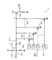
図1はラジオ受信機の一実施形態のブロック図である。同図に示すように、本実施形態のラジオ受信機は、FM放送を受信するFM受信部1と、AM放送を受信するAM受信部2とを備えている。FM受信部1は、高周波増幅回路101、混合回路102、局部発振回路103、選局回路104、中間周波増幅回路105、FM検波回路106、ステレオ復調回路107、ディエンファシス回路108L、108R、低周波増幅回路109L、109R、およびスピーカ110L、110Rを含んで構成されている。一方、AM受信部2は、高周波増幅回路201、混合回路202、局部発振回路203、選局回路204、中間周波増幅回路205、AM検波回路206、低周波増幅回路207、およびスピーカ208を含んで構成されている。
【0015】
また、図1に示すラジオ受信機は、アンテナ3、クロック発生回路4、サンプリング同調回路5、および同調発振回路6を備えており、これらはFM受信部1とAM受信部2の双方で利用される。
【0016】
次に、FM受信部1とAM受信部2の構成および動作について詳細に説明する。
【0017】
(1)FM受信部の構成および動作について
FM受信部1の高周波増幅回路101は、アンテナ3で受信した放送波のうち特定の帯域の放送波を選択的に増幅する。混合回路102、局部発振回路103および選局回路104は周波数変換器を構成しており、高周波増幅回路101から出力される周波数fc の搬送波信号と局部発振回路103から出力される周波数fL の局部発振信号とを混合し、変調内容を変えずに周波数変換を行ってfL −fc の中間周波信号を出力する。FM放送を受信する場合には、中間周波信号の周波数は例えば10.7MHzに設定される。この周波数は、FM放送の受信時は常に固定である。
【0018】
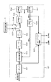
図2は、局部発振回路103と選局回路104の詳細構成を示すブロック図であり、PLL周波数シンセサイザー方式の電子選局を行う例を示している。基準発振器301から出力された基準発振信号はプリスケーラ302で例えば4分周されて局部発振回路103内の位相比較器303に入力される。また、局部発振回路103内の電圧制御発振回路(VCO)304から出力された局部発振信号は、プリスケーラ305に入力されて例えば4分周された後、プログラマブルカウンタ306で選局周波数に応じた分周比で分周されて位相比較器303に入力される。位相比較器303は、プリスケーラ302の出力の位相とプログラマブルカウンタ306の出力の位相とを比較し、位相差に応じた電圧をローパスフィルタ307を介して電圧制御発振回路304に入力する。
【0019】
以上により、電圧制御発振回路304から出力される局部発振信号は基準発振信号に同期するように制御される。また、制御回路308は、プログラマブルカウンタ306に分周比を設定するとともに、表示部309に選局周波数などの各種情報を表示させる。
【0020】
図1に示す混合回路102の出力はスイッチSW1に入力される。スイッチSW1は、FM放送の受信時には接点p側に設定され、AM放送の受信時には接点q側に設定される。したがって、FM放送の受信時には、混合回路102の出力はサンプリング同調回路5に入力される。サンプリング同調回路5は、混合回路102の出力の中から中間周波数成分のみを抽出する。
【0021】
図3は、サンプリング同調回路5の詳細構成を示す回路図である。同図に示すように、サンプリング同調回路5は、16出力を有するリングカウンタ401と、リングカウンタ401の各出力に接続されるMOSトランジスタ402と、各MOSトランジスタ402のドレイン端子に接続されるコンデンサ403と、並列接続された抵抗404およびコンデンサ405とを含んで構成されている。
【0022】
図4は、リングカウンタ401の出力変化を示す波形図である。同図に示すように、リングカウンタ401は、図1のクロック発生回路4から出力される基準クロックの16周期に1回の割合でパルスを出力する。より詳細には、リングカウンタ401は各出力端子から基準クロックの16倍の周期を有するパルスを出力する。また、各出力端子から出力されるパルスの位相を基準クロックの1クロック分ずつずらしている。
【0023】
リングカウンタ401の各出力は、図3に示すように、対応するMOSトランジスタ402のゲート端子に入力される。リングカウンタ401の各出力端子から出力されるパルスの位相は互いにずれているため、MOSトランジスタ402がオンする時期もそれぞれ異なっており、MOSトランジスタ402に接続されたコンデンサ403は、MOSトランジスタ402のオン・オフに応じて充放電を繰り返す。
【0024】
例えば、サンプリング同調回路5に基準クロックを16分周した信号と周波数が等しい信号Vinが入力された場合には、図3のa点の電圧は図4のように階段状に変化する。一方、基準クロックを16分周した信号と異なる周波数の信号がサンプリング同調回路5に入力された場合には、各周期ごとに図3のa点の電圧が変化するため、やがてa点の電位はゼロ電位に収束する。このように、図3のようなサンプリング同調回路を構成することにより、リングカウンタ401の出力周波数、すなわち基準クロックの1/16の周波数と等しい周波数成分のみを抽出することができる。
【0025】
なお、図3のa点のラインはインピーダンスが高いため、入力インピーダンスが低い後段の回路に直接接続すると出力波形をそのままの形で取り出すことができない。このため、a点のラインを図3のようにFET406でいったん受けて、このFET406のソース端子を後段の回路に接続するのが望ましい。なお、図3のキャパシタ407は、混合回路102の出力Vinに含まれる直流分をカットするためのものであり、抵抗408および409はFET406に適当なバイアスを与えるためのものである。
【0026】
このように、サンプリング同調回路5は、リングカウンタ401やMOSトランジスタ402などの半導体化しやすい部品のみで構成されているため、回路全体を容易にチップ化することができる。また、図3の回路では、リングカウンタ401の出力数を増やして1周期内のサンプリング数を増やすことにより、同調精度を容易に上げることができる。逆に、高精度の同調が不要の場合には、1周期内のサンプリング数を減らせばよく、サンプリング数を減らすことで回路規模を削減できる。
【0027】
また、図3に示すサンプリング同調回路5は、デジタル的に同調を行うため、構成部品の温度特性等の影響を受けることがなく、常に安定した精度で同調を行える。さらに、増幅回路を持たないため、発振するおそれもない。
【0028】
サンプリング同調回路5に入力される基準クロックは図1に示すクロック発生回路4で生成される。クロック発生回路4は、電圧制御発振回路(VCO)451と、プログラマブルカウンタ(PC)452と、基準発振器453と、位相比較器454と、ローパスフィルタ(LPF)455とを含んで構成されている。電圧制御発振回路451は基準クロックを出力し、プログラマブルカウンタ452は予め設定された分周比で基準クロックを分周する。位相比較器454は、プログラマブルカウンタ452の出力と、基準発振器453からの基準発振信号とを位相比較し、位相差に応じた電圧をローパスフィルタ455を介して電圧制御発振回路451に入力する。電圧制御発振回路451は、ローパスフィルタ455の出力電圧に応じて基準クロックの周波数を変更し、基準クロックが基準発振信号に同期するように制御する。
【0029】
このように、プログラマブルカウンタ452の分周比が任意に設定可能なクロック発生回路4とサンプリング同調回路5とを組み合わせることにより、同調周波数の変更を容易に行うことができ、かつ所望の同調周波数を正確に設定することができる。また、図3に示すサンプリング同調回路5のQは、Q=πfCRN(Cはキャパシタ403の静電容量、Rは抵抗404の抵抗値、Nはサンプリング数)で表され、基準クロックの周波数が高くなるほどQが大きくなるため、同調周波数を変更しても帯域幅Δf=f/Qを常に一定にでき、広範囲の周波数に対して同精度で同調を行える。
【0030】
サンプリング同調回路5を通過した10.7MHzの中間周波信号は、図1に示すように、中間周波増幅回路105で増幅された後にFM検波回路106に入力される。FM検波回路106は、中間周波信号を変調前のステレオ複合信号に変換する。このステレオ複合信号は、L信号成分と、R信号成分と、19kHzのパイロット信号とを合成したものである。このステレオ複合信号はステレオ復調回路107に入力されてL信号とR信号とに分離再生される。
【0031】
図5はステレオ復調回路107の詳細構成を示すブロック図である。同図に示すように、ステレオ復調回路107は、プリアンプ501と、位相比較器502と、ローパスフィルタ503と、DCアンプ504と、分周器505〜508と、スイッチング回路509とを含んで構成され、DCアンプ504の出力は同調発振回路6に入力される。同調発振回路6は、後述するように所定周波数、例えば456kHzで発振動作を行い、その発振出力は分周器505に入力される。分周器505〜507は同調発振回路6の出力を分周して38kHzの正弦波信号を生成し、分周器508はさらに2分周して19kHzの正弦波信号を生成する。位相比較器502は、ステレオ複合信号に含まれるパイロット信号と分周器508の出力とを位相比較し、位相差に応じた電圧を出力する。この出力はローパスフィルタ503を介してDCアンプ504に入力される。
【0032】
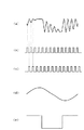
図6はステレオ復調回路107内の各部の信号波形図の一例であり、図6(a)はプリアンプ501に入力されるステレオ複合信号の波形、図6(b)は分周器507の出力の波形、図6(c)は分周器507の出力の位相を半周期ずらした信号の波形、図6(d)はスイッチング回路509から出力されるL信号の波形、図6(e)はスイッチング回路509から出力されるR信号の波形を示している。
【0033】
図6(a)に示すように、ステレオ復調回路107に入力されるステレオ複合信号は、L信号とR信号を38kHzの副搬送波で変調したものである。このため、ステレオ復調回路107内部の分周器505〜507で38kHzのスイッチング信号を生成し、生成したスイッチング信号に同期してステレオ複合信号を取り込むことで、図6(d)および(e)のように、L信号とR信号を取り出すことができる。なお、図6(d)、(e)では、説明を簡略化するために、L信号を正弦波で、R信号を矩形波で表している。
【0034】
図7は図1に示す同調発振回路6の中に含まれるGIC(Generalized Inpedance Converter )の動作原理を説明する原理図である。同図に示すように、GIC600は、2個のオペアンプ601および602と、5個のインピーダンスZ1 〜Z5 とで構成され、図示の1−1′間のインピーダンスZは(1)式で表される。
【0035】
Z=(Z1 ・Z3 ・Z5 )/(Z2 ・Z4 ) …(1)
インピーダンスZ2 、Z4 のいずれかにキャパシタを、それ以外のインピーダンスに抵抗を割り当てることにより、図7の回路は等価的にインダクタンスと同じ性質を示す。
【0036】
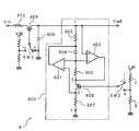
図8は図1の同調発振回路6の詳細構成を示す回路図、図9は図8の等価回路図である。図8に示すように、抵抗605と607の間にはFET606が接続され、このFET606のゲート電圧を制御することにより、FET606のドレイン−ソース間の抵抗値が可変制御される。このFET606のゲート端子には、図1に示すスイッチSW2が接続されている。このスイッチSW2は、FM放送を受信する場合には接点r側に設定され、AM放送を受信する場合には接点s側に設定される。接点r側のラインは、図5に示すようにステレオ復調回路107内部のDCアンプ504に接続されており、同調発振回路6はFM放送の受信時にはDCアンプ504の出力に応じて発振周波数を可変制御する。
【0037】
また、GIC600と並列にキャパシタ608が接続されて等価的な並列共振回路が構成されており、さらに、GIC600とキャパシタ608の一端には、FET609を介して入力抵抗610が接続されている。FET609のゲート端子にはスイッチSW3が接続され、このスイッチSW3は、FM放送を受信する場合には接点t側に設定され、AM放送を受信する場合には接点u側に設定される。
【0038】
FET609として、例えばnチャネル−エンハンスメント型のMOSFETを用いた場合には、ゲート端子をローレベルにするとFET609はカットオフ状態となり、図8に示す同調発振回路6の入力抵抗610の抵抗値はみかけ上無限大になる。
【0039】
ところで、図8に示す同調発振回路6のQは(2)式で表される。
【0040】
Q=R/(ωL) …(2)
ただし、Rは入力抵抗610の抵抗値、LはGIC600のインダクタンスを示している。同調発振回路6を発振動作させたい場合には、(2)式に示すQを所定値以上に設定する必要がある。したがって、図8に示すスイッチSW3を接点t側に設定して入力抵抗610の抵抗値を無限大にすると、Qも無限大になり、同調発振回路6は安定に発振動作を行う。したがって、この状態でFET606のゲート電圧を制御することにより、同調発振回路6は、FM放送の受信時には電圧制御発振回路として機能する。
【0041】
なお、図8に示す同調発振回路5では、FET609をオン・オフさせることにより入力抵抗610の抵抗値をみかけ上変化させているが、FET609を設ける代わりに、入力抵抗610として可変抵抗を用いてその抵抗値を調整してもよい。
【0042】
また、同調発振回路6の出力Vout には、図1に示すようにスイッチSW4が接続され、このスイッチSW4はFM放送の受信時には接点v側に設定される。したがって、同調発振回路6の出力はスイッチSW4の接点vを通って図5に示したステレオ復調回路107内部の分周回路505に入力される。
【0043】
ステレオ復調回路107で分離再生されたL信号およびR信号は、図1に示すようにそれぞれ別々にディエンファシス回路108L、108Rに入力され、高域部を減衰させてSN比の改善を図った後、低周波増幅回路109L、109Rを経てスピーカ110L、110Rから音声出力される。
【0044】
(2)AM受信部の構成および動作について
AM放送を受信する場合には、図1に示すスイッチSW1は接点q側に設定される。したがって、アンテナ3で受信した受信信号はスイッチSW1を介してサンプリング同調回路5に入力される。上述したように、サンプリング同調回路5は、受信信号の中から基準クロックと同一周波数成分のみを抽出する。なお、FM放送を受信する場合は、クロック発生回路4から出力される基準クロックの周波数は常に固定に設定されるが、AM放送を受信する場合は、選局する周波数に応じて基準クロックの周波数を変化させる必要がある。より具体的には、AM受信時には、基準クロックの周波数は選局を希望する周波数の16倍(サンプリング数Nが「16」の場合)の周波数に設定される。
【0045】
サンプリング同調回路5の出力は、混合回路202、局部発振回路203および選局回路204からなる周波数変換器に入力され、例えば450kHzの中間周波信号に変換される。局部発振回路203は、FM受信部1の局部発振回路103と同じように構成され、不図示の電圧制御発振回路(VCO)から出力される局部発振信号を不図示の基準発振器から出力される基準発振信号に同期させる処理を行う。選局回路204は、AM放送の周波数範囲(例えば530〜1700kHz)の中で選局を行う。
【0046】
なお、サンプリング同調回路5の同調周波数と、局部発振信号の発振周波数とは連動して変化し、例えば周波数fの放送波を受信する場合は、サンプリング同調回路5の同調周波数はfに設定され、局部発振信号の発振周波数は例えばf+450kHzに設定される。
【0047】
混合回路202から出力された中間周波信号は、図8に詳細を示す同調発振回路6に入力される。AM放送の受信時には、図8に示すスイッチSW3が接点u側に設定されてFET609がオンし、混合回路202からの中間周波信号は入力抵抗610を介して抵抗603の一端に印加される。また、スイッチSW2は接点s側に設定され、FET606のゲート端子には、抵抗7および8の分圧比で定まる電圧が印加される。したがって、抵抗7および8の分圧比を予め調整しておくことで、図8に示した同調発振回路6は、FET609を介して入力された信号の中から450kHzの中間周波信号のみを抽出する同調動作を行う。
【0048】
また、AM放送の受信時には、図1に示すスイッチSW4は接点w側に設定され、同調発振回路6を通過した信号はスイッチSW4の接点wを介して中間周波増幅回路205に入力されてゲイン調整が行われた後にAM検波回路206に入力される。AM検波回路206は、ダイオード等を用いて中間周波信号を低周波信号に変換し、変換した低周波信号は低周波増幅回路207で増幅されてスピーカ208から音声出力される。
【0049】
このように、本実施形態では、AM放送波の選択同調をサンプリング同調回路5を用いて行っており、従来のようなLC共振回路を利用した同調を行っていないため、アンテナの容量による影響を受けることがない。したがって、カーラジオ等のようにロッドアンテナをサンプリング同調回路5に直接接続することも可能であり、周波数変換器や中間周波増幅回路205などの後段側の回路に不要な妨害電波が混入するおそれもなくなる。また、AM放送を受信する際には、PLL制御によって、サンプリング同調回路5の同調周波数すなわち基準クロックの周波数と局部発振回路203から出力される局部発振信号の周波数とを連動して変化させるため、混合回路202から出力される中間周波信号の周波数を常に一定にすることができる。したがって、従来問題とされたトラッキングエラーが起きなくなる。
【0050】
また、本実施形態では、サンプリング同調回路5をFM放送の受信時には中間周波フィルタとして利用し、AM放送の受信時には初段の選択同調回路として利用するため、中間周波フィルタや選択同調回路を別個に設ける必要がなくなる。同様に、同調発振回路6をFM放送の受信時にはステレオ復調用の電圧制御発振回路として利用し、AM放送の受信時には中間周波フィルタとして利用するため、電圧制御発振回路や中間周波フィルタを別個に設ける必要がなくなり、構成部品を削減できるとともに、受信機の小型化が可能となる。
【0051】
上述した実施形態では、AM/FM兼用ラジオ受信機の構成を示したが、AM専用ラジオ受信機、あるいはFM専用ラジオ受信機の場合にも本発明は適用可能である。例えば、AM専用ラジオ受信機の場合、図1に示すFM受信部1を省略し、図1の並列接続された抵抗10とキャパシタ11の一端をサンプリング同調回路5に直接接続すればよい。一方、FM専用ラジオ受信機の場合、図1に示すAM受信部2を省略し、図1の混合回路102の出力をサンプリング同調回路5に直接入力すればよい。また、FM受信時には、クロック発生回路4から出力される基準クロックの周波数は常に一定であるため、プログラマブルカウンタ452の代わりに、分周比が固定の分周器を用いてもよい。
【0052】
また、上述した実施形態では、スーパーヘテロダイン方式のラジオ受信機の一例について説明したが、本発明は、スーパーヘテロダイン方式以外のラジオ受信機にも適用可能である。例えば、アンテナ3で受信したFM放送波を、中間周波信号に変換することなくサンプリング同調回路5に入力して選択同調処理を行い、サンプリング同調回路5の出力に基づいて検波処理を行った後、検波して得られたステレオ復調信号をL信号とR信号に分離再生する際に、図1に示した同調発振回路6を用いてもよい。あるいは、アンテナ3で受信したAM放送波をサンプリング同調回路5で選択同調した後、中間周波信号に変換することなく図1に示す同調発振回路6に入力してもよい。
【0053】
なお、図3に示したサンプリング同調回路5において、MOSトランジスタ402の代わりに、図10に示すようにCMOS構成のトランジスタ402′を用いてもよい。CMOS構成のトランジスタ402′を用いた場合には、寄生容量の影響を受けにくくなる。また、サンプリング同調回路5を構成する全素子をCMOSプロセスで形成できるため、チップ化する場合のプロセスを簡易化できる。
【0054】
【発明の効果】
以上詳細に説明したように、本発明によれば、アンテナで受信した受信信号を基準クロックでサンプリングし、受信信号の中から基準クロックと同一周波数成分のみを抽出するため、従来のようにLC共振回路を用いずに同調回路を構成できる。したがって、アンテナの容量による影響を受けることなく、アンテナを直接同調回路に接続して所望の周波数に同調させることができる。また、デジタル的な同調処理を行うため、構成部品の温度特性等の影響を受けることがない。さらに、基準クロックの周波数を変えるだけで同調周波数を変更でき、かつ同調周波数に応じてQが変化するため、広帯域にわたって同一精度で同調を行うことができる。
【図面の簡単な説明】
【図1】ラジオ受信機の一実施形態のブロック図である。
【図2】局部発振回路と選局回路の詳細構成を示すブロック図である。
【図3】中間周波フィルタの詳細構成を示す回路図である。
【図4】リングカウンタの出力変化を示す波形図である。
【図5】ステレオ復調回路の詳細構成を示すブロック図である。
【図6】(a)〜(e)はステレオ復調回路内の各部の信号波形図である。
【図7】同調発振回路の中に含まれるGICの動作原理を説明する原理図である。
【図8】同調発振回路の詳細構成を示す回路図である。
【図9】図8の等価回路図である。
【図10】サンプリング同調回路の内部で使用されるCMOS構成のトランジスタの一例を示す図である。
【符号の説明】
1 FM受信部
2 AM受信部
3 アンテナ
4 クロック発生回路
5 サンプリング同調回路
6 同調発振回路
101 高周波増幅回路
102 混合回路
103 局部発振回路
104 選局回路
105 中間周波増幅回路
106 FM検波回路
107 ステレオ復調回路
108L、108R ディエンファシス回路
109L、109R 低周波増幅回路
110L、110R スピーカ
201 同調回路
202 混合回路
203 局部発振回路
204 選局回路
205 中間周波増幅回路
206 AM検波回路
207 低周波増幅回路
208 スピーカ[0001]
BACKGROUND OF THE INVENTION
The present invention relates to a radio receiver including a sampling tuning circuit that extracts only the same frequency component as a reference clock.
[0002]
[Prior art]
A tuning circuit is provided inside the radio receiver so that only a desired frequency radio wave can be selected. However, since only one tuning circuit is provided and the frequency selectivity is not good and noise cannot be completely removed, a plurality of tuning circuits are often provided inside the receiver. For example, in a superheterodyne AM receiver, a tuning circuit is provided in each of an antenna input circuit, a high frequency amplifier circuit, and an intermediate frequency amplifier circuit.
[0003]
[Problems to be solved by the invention]
By the way, when the antenna of the AM radio receiver is configured with a rod antenna like a car radio, the capacity of the antenna changes depending on the length of the antenna, and even if a tuning circuit is provided in the antenna input circuit, I can't get along well. For this reason, there is also proposed a circuit in which a high frequency signal from an antenna is received by an FET without being tuned and amplified by an FET without providing a tuning circuit at the first stage of the radio receiver, and is tuned on the subsequent stage side of the FET. . However, when tuning is not performed at the first stage of the radio receiver, various frequency radio waves are input to the tuning circuit provided on the rear stage side, so that desired frequency components are disturbed and cannot be extracted with high accuracy.
[0004]
Also, conventional AM / FM combined radio receivers are generally provided with separate tuning circuits for AM reception and FM reception, respectively, which increases the number of parts and hinders downsizing of the receiver. It was.
[0005]
Further, the conventional tuning circuit is generally configured to include an LC resonance circuit, and Q is always kept constant even when the tuning frequency changes. For this reason, the higher the tuning frequency, the wider the bandwidth, and there is a problem that the bandwidth changes according to the tuning frequency.
[0006]
The present invention has been created in view of the above points, and an object of the present invention is to provide a radio equipped with a tuning circuit that can be tuned with high accuracy over a wide band and can be used for both AM reception and FM reception. To provide a receiver.
[0007]
[Means for Solving the Problems]
In order to solve the above-described problem, a radio receiver according to
[0008]
The radio receiver according to
[0009]
The radio receiver according to claim 3 is a receiver capable of receiving AM broadcasting, and a sampling tuning circuit is directly connected to an antenna, for example, and only frequency components desired to be selected are extracted from received signals received by the antenna. To do.
[0010]
The radio receiver according to
[0011]
The radio receiver of claim 5 is a receiver capable of receiving AM broadcast and FM broadcast, and switches the input of the sampling tuning circuit depending on which one is received. Specifically, when receiving FM broadcasting, an FM intermediate frequency signal, which is a result of frequency conversion performed by the FM front end unit, is input to the sampling tuning circuit, and the sampling tuning circuit is used as an intermediate frequency filter. On the other hand, when receiving an AM broadcast, the received signal received by the antenna is input to the sampling tuning circuit as it is to tune the tuning to the desired frequency. Further, the frequency of the reference clock is fixed at the time of FM broadcast reception, and the frequency of the reference clock is changed in accordance with the frequency desired for channel selection at the time of AM broadcast reception.
[0012]
The radio receiver according to
[0013]
DETAILED DESCRIPTION OF THE INVENTION
Hereinafter, a radio receiver to which the present invention is applied will be specifically described with reference to the drawings.
[0014]
FIG. 1 is a block diagram of an embodiment of a radio receiver. As shown in the figure, the radio receiver of the present embodiment includes an
[0015]
The radio receiver shown in FIG. 1 includes an antenna 3, a
[0016]
Next, the configuration and operation of the
[0017]
(1) Configuration and operation of FM receiver
The high
[0018]
FIG. 2 is a block diagram showing the detailed configuration of the
[0019]
As described above, the local oscillation signal output from the voltage controlled oscillation circuit 304 is controlled to synchronize with the reference oscillation signal. The control circuit 308 sets a frequency division ratio in the programmable counter 306 and causes the display unit 309 to display various information such as a channel selection frequency.
[0020]
The output of the
[0021]
FIG. 3 is a circuit diagram showing a detailed configuration of the sampling tuning circuit 5. As shown in the figure, the sampling tuning circuit 5 includes a
[0022]
FIG. 4 is a waveform diagram showing changes in the output of the
[0023]
Each output of the
[0024]
For example, when a signal Vin having the same frequency as the signal obtained by dividing the reference clock by 16 is input to the sampling tuning circuit 5, the voltage at point a in FIG. 3 changes stepwise as shown in FIG. On the other hand, when a signal having a frequency different from the signal obtained by dividing the reference clock by 16 is input to the sampling tuning circuit 5, the voltage at the point a in FIG. It converges to zero potential. Thus, by configuring the sampling tuning circuit as shown in FIG. 3, only the frequency component equal to the output frequency of the
[0025]
Since the line at point a in FIG. 3 has a high impedance, the output waveform cannot be extracted as it is when directly connected to a subsequent circuit having a low input impedance. For this reason, it is desirable that the point a line is once received by the
[0026]
As described above, the sampling tuning circuit 5 is composed of only components that are easily semiconductorized, such as the
[0027]
Further, since the sampling tuning circuit 5 shown in FIG. 3 is digitally tuned, it is not affected by the temperature characteristics of the component parts and can always be tuned with stable accuracy. Further, since there is no amplifier circuit, there is no possibility of oscillation.
[0028]
The reference clock input to the sampling tuning circuit 5 is generated by the
[0029]
As described above, by combining the
[0030]
The 10.7 MHz intermediate frequency signal that has passed through the sampling tuning circuit 5 is amplified by the intermediate
[0031]
FIG. 5 is a block diagram showing a detailed configuration of the
[0032]
6 is an example of a signal waveform diagram of each part in the
[0033]
As shown in FIG. 6A, the stereo composite signal input to the
[0034]
FIG. 7 is a principle diagram for explaining the operating principle of a GIC (Generalized Impedance Converter) included in the
[0035]
Z = (Z1, Z3, Z5) / (Z2, Z4) (1)
By assigning a capacitor to one of the impedances Z2 and Z4 and a resistance to the other impedances, the circuit of FIG. 7 equivalently exhibits the same property as the inductance.
[0036]
8 is a circuit diagram showing a detailed configuration of the
[0037]
In addition, an equivalent parallel resonant circuit is configured by connecting a
[0038]
For example, when an n-channel-enhancement type MOSFET is used as the
[0039]
Incidentally, Q of the
[0040]
Q = R / (ωL) (2)
Here, R represents the resistance value of the
[0041]
In the tuning oscillation circuit 5 shown in FIG. 8, the resistance value of the
[0042]
Further, as shown in FIG. 1, a switch SW4 is connected to the output Vout of the
[0043]
The L signal and the R signal separated and reproduced by the
[0044]
(2) Configuration and operation of AM receiver
When receiving the AM broadcast, the switch SW1 shown in FIG. 1 is set to the contact q side. Therefore, the received signal received by the antenna 3 is input to the sampling tuning circuit 5 via the switch SW1. As described above, the sampling tuning circuit 5 extracts only the same frequency component as the reference clock from the received signal. When receiving an FM broadcast, the frequency of the reference clock output from the
[0045]
The output of the sampling tuning circuit 5 is input to a frequency converter including a
[0046]
Note that the tuning frequency of the sampling tuning circuit 5 and the oscillation frequency of the local oscillation signal change in conjunction with each other. For example, when receiving a broadcast wave of the frequency f, the tuning frequency of the sampling tuning circuit 5 is set to f, The oscillation frequency of the local oscillation signal is set to, for example, f + 450 kHz.
[0047]
The intermediate frequency signal output from the mixing
[0048]
When receiving the AM broadcast, the switch SW4 shown in FIG. 1 is set to the contact w side, and the signal passing through the
[0049]
As described above, in this embodiment, the AM broadcast wave is selectively tuned using the sampling tuning circuit 5 and is not tuned using the conventional LC resonance circuit. I do not receive it. Therefore, it is possible to connect the rod antenna directly to the sampling tuning circuit 5 as in a car radio or the like, and there is a possibility that unnecessary jamming radio waves may be mixed in the downstream circuit such as the frequency converter and the intermediate
[0050]
In this embodiment, the sampling tuning circuit 5 is used as an intermediate frequency filter when receiving FM broadcasts, and is used as a first stage selective tuning circuit when receiving AM broadcasts. Therefore, an intermediate frequency filter and a selective tuning circuit are separately provided. There is no need. Similarly, the
[0051]
In the embodiment described above, the configuration of the AM / FM combined radio receiver is shown. However, the present invention can also be applied to an AM dedicated radio receiver or an FM dedicated radio receiver. For example, in the case of an AM dedicated radio receiver, the
[0052]
In the above-described embodiment, an example of a superheterodyne radio receiver has been described. However, the present invention can also be applied to radio receivers other than the superheterodyne radio receiver. For example, after the FM broadcast wave received by the antenna 3 is input to the sampling tuning circuit 5 without being converted into an intermediate frequency signal, selective tuning processing is performed, and after detection processing is performed based on the output of the sampling tuning circuit 5, When the stereo demodulated signal obtained by detection is separated and reproduced into an L signal and an R signal, the
[0053]
In the sampling tuning circuit 5 shown in FIG. 3, a
[0054]
【The invention's effect】
As described above in detail, according to the present invention, the received signal received by the antenna is sampled by the reference clock, and only the same frequency component as the reference clock is extracted from the received signal. A tuning circuit can be configured without using a circuit. Therefore, the antenna can be directly connected to the tuning circuit and tuned to a desired frequency without being affected by the capacity of the antenna. Further, since digital tuning processing is performed, there is no influence of the temperature characteristics of the component parts. Furthermore, since the tuning frequency can be changed only by changing the frequency of the reference clock, and Q changes according to the tuning frequency, tuning can be performed with the same accuracy over a wide band.
[Brief description of the drawings]
FIG. 1 is a block diagram of one embodiment of a radio receiver.
FIG. 2 is a block diagram showing a detailed configuration of a local oscillation circuit and a channel selection circuit.
FIG. 3 is a circuit diagram showing a detailed configuration of an intermediate frequency filter.
FIG. 4 is a waveform diagram showing a change in output of a ring counter.
FIG. 5 is a block diagram showing a detailed configuration of a stereo demodulation circuit.
FIGS. 6A to 6E are signal waveform diagrams of respective parts in the stereo demodulation circuit.
FIG. 7 is a principle diagram for explaining an operation principle of a GIC included in a tuning oscillation circuit.
FIG. 8 is a circuit diagram showing a detailed configuration of a tuning oscillation circuit.
FIG. 9 is an equivalent circuit diagram of FIG.
FIG. 10 is a diagram showing an example of a transistor having a CMOS configuration used in the sampling tuning circuit.
[Explanation of symbols]
1 FM receiver
2 AM receiver
3 Antenna
4 Clock generation circuit
5 Sampling tuning circuit
6 Tuning oscillation circuit
101 High frequency amplifier circuit
102 Mixing circuit
103 Local oscillator circuit
104 Channel selection circuit
105 Intermediate frequency amplifier
106 FM detection circuit
107 Stereo demodulation circuit
108L, 108R De-emphasis circuit
109L, 109R Low frequency amplifier circuit
110L, 110R Speaker
201 Tuning circuit
202 Mixing circuit
203 Local oscillator circuit
204 Tuning circuit
205 Intermediate frequency amplifier
206 AM detection circuit
207 Low frequency amplifier circuit
208 Speaker
Claims (4)
基準クロックの周期の整数倍の周期を有し互いに位相のずれた複数のパルス信号を出力するパルス発生回路と、
このパルス発生回路から出力された前記パルス信号で前記受信信号をサンプリングした結果に基づいて、前記受信信号の中から前記パルス信号と同一周波数成分のみを抽出するサンプリング同調回路とを備え、
前記サンプリング同調回路は、AM放送の受信時には、選択同調あるいは周波数変換することなく入力された前記受信信号の中から選局を希望する周波数成分のみを抽出し、
前記サンプリング同調回路の出力に基づいて検波処理を行うことを特徴とするラジオ受信機。 In a radio receiver that performs detection processing by extracting only the frequency components desired to be selected from the received signal received by the rod antenna,
A pulse generation circuit that outputs a plurality of pulse signals that have a period that is an integral multiple of the period of the reference clock and that are out of phase with each other;
A sampling tuning circuit that extracts only the same frequency component as the pulse signal from the reception signal based on the result of sampling the reception signal with the pulse signal output from the pulse generation circuit;
The sampling tuning circuit extracts only a frequency component desired to be selected from the received signal input without selective tuning or frequency conversion when receiving an AM broadcast,
A radio receiver characterized in that a detection process is performed based on an output of the sampling tuning circuit.
前記受信信号を低周波のFM中間周波信号に変換するFMフロントエンド部と、
前記FM中間周波信号に対して検波処理を行うFM検波部と、
FM放送の受信時には前記FMフロントエンド部の出力を前記サンプリング同調回路に導いて前記FMフロントエンド部の出力の中から予め定めた中間周波数成分のみを抽出して前記FM検波部に供給し、AM放送の受信時には前記受信信号を選択同調あるいは周波数変換することなく前記サンプリング同調回路に導く受信切換手段と、
FM放送の受信時には予め定めた一定周波数の前記基準クロックを出力し、AM放送の受信時には選局を希望する周波数に対応した周波数の前記基準クロックを出力する基準クロック発生回路と、
をさらに備えることを特徴とするラジオ受信機。 In claim 1,
An FM front end for converting the received signal into a low frequency FM intermediate frequency signal;
An FM detector for performing a detection process on the FM intermediate frequency signal;
When receiving an FM broadcast, the output of the FM front end unit is guided to the sampling tuning circuit, and only a predetermined intermediate frequency component is extracted from the output of the FM front end unit and supplied to the FM detection unit. A reception switching means for guiding the received signal to the sampling tuning circuit without selective tuning or frequency conversion at the time of receiving a broadcast;
A reference clock generating circuit for outputting the reference clock having a predetermined frequency when receiving FM broadcast, and outputting the reference clock having a frequency corresponding to a frequency desired to be selected when receiving AM broadcast;
A radio receiver further comprising:
AM放送の受信時に、選局を希望する周波数に応じた周波数の局部発振信号を出力する局部発振回路と、
AM放送の受信時に、前記サンプリング同調回路の出力を前記局部発振信号に基づいて低周波のAM中間周波数に変換する周波数変換器とを備え、
AM放送の受信時には、前記基準クロックの周波数と前記局部発振信号の周波数とを連動して変化させることを特徴とするラジオ受信機。 In claim 1 or 2,
A local oscillation circuit that outputs a local oscillation signal having a frequency corresponding to a frequency desired to be selected when receiving an AM broadcast;
A frequency converter for converting an output of the sampling tuning circuit into a low AM intermediate frequency based on the local oscillation signal when receiving an AM broadcast;
A radio receiver characterized in that when receiving an AM broadcast, the frequency of the reference clock and the frequency of the local oscillation signal are changed in conjunction with each other.
前記サンプリング同調回路は、前記パルス発生回路から出力される各パルス信号に対応して設けられた各パルス信号に同期して前記受信信号の信号レベルに応じた電荷を蓄積する複数のキャパシタを備えることを特徴とするラジオ受信機。 In any one of Claims 1-3,
The sampling tuning circuit includes a plurality of capacitors for accumulating charges corresponding to the signal level of the received signal in synchronization with each pulse signal provided corresponding to each pulse signal output from the pulse generation circuit. A radio receiver featuring.
Priority Applications (1)
| Application Number | Priority Date | Filing Date | Title |
|---|---|---|---|
| JP33024996A JP3676527B2 (en) | 1996-11-25 | 1996-11-25 | Radio receiver |
Applications Claiming Priority (1)
| Application Number | Priority Date | Filing Date | Title |
|---|---|---|---|
| JP33024996A JP3676527B2 (en) | 1996-11-25 | 1996-11-25 | Radio receiver |
Publications (2)
| Publication Number | Publication Date |
|---|---|
| JPH10163898A JPH10163898A (en) | 1998-06-19 |
| JP3676527B2 true JP3676527B2 (en) | 2005-07-27 |
Family
ID=18230532
Family Applications (1)
| Application Number | Title | Priority Date | Filing Date |
|---|---|---|---|
| JP33024996A Expired - Fee Related JP3676527B2 (en) | 1996-11-25 | 1996-11-25 | Radio receiver |
Country Status (1)
| Country | Link |
|---|---|
| JP (1) | JP3676527B2 (en) |
Families Citing this family (2)
| Publication number | Priority date | Publication date | Assignee | Title |
|---|---|---|---|---|
| JP3646598B2 (en) | 1999-12-21 | 2005-05-11 | 三菱電機株式会社 | Digital FM stereo demodulator |
| JP2024017985A (en) * | 2022-07-28 | 2024-02-08 | カヤバ株式会社 | Fluid property detection device |
-
1996
- 1996-11-25 JP JP33024996A patent/JP3676527B2/en not_active Expired - Fee Related
Also Published As
| Publication number | Publication date |
|---|---|
| JPH10163898A (en) | 1998-06-19 |
Similar Documents
| Publication | Publication Date | Title |
|---|---|---|
| US7505746B2 (en) | IC receiver to minimize tracking error | |
| EP0196697B1 (en) | Am receiver | |
| US20090128240A1 (en) | Oscillator, pll circuit, receiver and transmitter | |
| KR910003230B1 (en) | Mujlti-band fm receiver for receiving fm broadcasting signals and tv broadcasting sound signals | |
| US5387913A (en) | Receiver with digital tuning and method therefor | |
| EP1172933A2 (en) | Automatic filter tuning control system | |
| US20010038317A1 (en) | PLL-tuning system | |
| JPS61251313A (en) | Electronic tuning type fm receiver | |
| JP3676527B2 (en) | Radio receiver | |
| JP3592469B2 (en) | Radio receiver | |
| JPH0389720A (en) | Radio receiver | |
| JP4076558B2 (en) | AM / FM radio receiver and local oscillation circuit used therefor | |
| KR20010022059A (en) | Radio receiver | |
| JP3676528B2 (en) | Radio receiver | |
| JP3859767B2 (en) | FM stereo transmitter | |
| JP3223062B2 (en) | FM multiplex signal receiving circuit | |
| KR970008805B1 (en) | Pll frequency synthesizer | |
| JP2005500732A (en) | Stereo decoder | |
| JP2000082779A (en) | Receiver | |
| JP2000299646A (en) | Double conversion tuner | |
| JPH0336139Y2 (en) | ||
| JPH0328624Y2 (en) | ||
| JPS61251314A (en) | Electronic tuning type receiver | |
| JPH05206734A (en) | Multi-band radio receiver ic | |
| JPH08195918A (en) | Digital/analog compatible receiver |
Legal Events
| Date | Code | Title | Description |
|---|---|---|---|
| A977 | Report on retrieval |
Free format text: JAPANESE INTERMEDIATE CODE: A971007 Effective date: 20040906 |
|
| A131 | Notification of reasons for refusal |
Free format text: JAPANESE INTERMEDIATE CODE: A131 Effective date: 20040921 |
|
| A521 | Written amendment |
Free format text: JAPANESE INTERMEDIATE CODE: A523 Effective date: 20041122 |
|
| TRDD | Decision of grant or rejection written | ||
| A01 | Written decision to grant a patent or to grant a registration (utility model) |
Free format text: JAPANESE INTERMEDIATE CODE: A01 Effective date: 20050426 |
|
| A61 | First payment of annual fees (during grant procedure) |
Free format text: JAPANESE INTERMEDIATE CODE: A61 Effective date: 20050428 |
|
| R150 | Certificate of patent or registration of utility model |
Free format text: JAPANESE INTERMEDIATE CODE: R150 |
|
| FPAY | Renewal fee payment (event date is renewal date of database) |
Free format text: PAYMENT UNTIL: 20090513 Year of fee payment: 4 |
|
| LAPS | Cancellation because of no payment of annual fees |