JP3673657B2 - Plasma display phosphor inspection apparatus and inspection method - Google Patents
Plasma display phosphor inspection apparatus and inspection method Download PDFInfo
- Publication number
- JP3673657B2 JP3673657B2 JP31552898A JP31552898A JP3673657B2 JP 3673657 B2 JP3673657 B2 JP 3673657B2 JP 31552898 A JP31552898 A JP 31552898A JP 31552898 A JP31552898 A JP 31552898A JP 3673657 B2 JP3673657 B2 JP 3673657B2
- Authority
- JP
- Japan
- Prior art keywords
- phosphor
- light
- plasma display
- wavelength
- filter
- Prior art date
- Legal status (The legal status is an assumption and is not a legal conclusion. Google has not performed a legal analysis and makes no representation as to the accuracy of the status listed.)
- Expired - Fee Related
Links
Images


Classifications
-
- G—PHYSICS
- G01—MEASURING; TESTING
- G01N—INVESTIGATING OR ANALYSING MATERIALS BY DETERMINING THEIR CHEMICAL OR PHYSICAL PROPERTIES
- G01N21/00—Investigating or analysing materials by the use of optical means, i.e. using sub-millimetre waves, infrared, visible or ultraviolet light
- G01N21/84—Systems specially adapted for particular applications
- G01N21/8422—Investigating thin films, e.g. matrix isolation method
-
- G—PHYSICS
- G01—MEASURING; TESTING
- G01N—INVESTIGATING OR ANALYSING MATERIALS BY DETERMINING THEIR CHEMICAL OR PHYSICAL PROPERTIES
- G01N21/00—Investigating or analysing materials by the use of optical means, i.e. using sub-millimetre waves, infrared, visible or ultraviolet light
- G01N21/84—Systems specially adapted for particular applications
- G01N21/88—Investigating the presence of flaws or contamination
-
- G—PHYSICS
- G06—COMPUTING; CALCULATING OR COUNTING
- G06T—IMAGE DATA PROCESSING OR GENERATION, IN GENERAL
- G06T7/00—Image analysis
- G06T7/0002—Inspection of images, e.g. flaw detection
- G06T7/0004—Industrial image inspection
-
- G—PHYSICS
- G01—MEASURING; TESTING
- G01N—INVESTIGATING OR ANALYSING MATERIALS BY DETERMINING THEIR CHEMICAL OR PHYSICAL PROPERTIES
- G01N21/00—Investigating or analysing materials by the use of optical means, i.e. using sub-millimetre waves, infrared, visible or ultraviolet light
- G01N21/84—Systems specially adapted for particular applications
- G01N21/8422—Investigating thin films, e.g. matrix isolation method
- G01N2021/8427—Coatings
-
- G—PHYSICS
- G01—MEASURING; TESTING
- G01N—INVESTIGATING OR ANALYSING MATERIALS BY DETERMINING THEIR CHEMICAL OR PHYSICAL PROPERTIES
- G01N21/00—Investigating or analysing materials by the use of optical means, i.e. using sub-millimetre waves, infrared, visible or ultraviolet light
- G01N21/84—Systems specially adapted for particular applications
- G01N21/88—Investigating the presence of flaws or contamination
- G01N21/8806—Specially adapted optical and illumination features
Landscapes
- Physics & Mathematics (AREA)
- General Physics & Mathematics (AREA)
- Engineering & Computer Science (AREA)
- Immunology (AREA)
- Health & Medical Sciences (AREA)
- Biochemistry (AREA)
- General Health & Medical Sciences (AREA)
- Chemical & Material Sciences (AREA)
- Life Sciences & Earth Sciences (AREA)
- Pathology (AREA)
- Analytical Chemistry (AREA)
- Quality & Reliability (AREA)
- Computer Vision & Pattern Recognition (AREA)
- Theoretical Computer Science (AREA)
- Mathematical Physics (AREA)
- Manufacture Of Electron Tubes, Discharge Lamp Vessels, Lead-In Wires, And The Like (AREA)
- Investigating Materials By The Use Of Optical Means Adapted For Particular Applications (AREA)
- Gas-Filled Discharge Tubes (AREA)
- Investigating, Analyzing Materials By Fluorescence Or Luminescence (AREA)
Description
【0001】
【発明の属する技術分野】
本発明はプラズマディスプレイの蛍光体塗布工程における塗布状態の検査を画像処理により行うプラズマディスプレイ蛍光体の検査装置および検査方法に関するものである。
【0002】
【従来の技術】
今後のマルチメディア時代の大型、高精度ディスプレイとして、プラズマディスプレイに対する期待が高まってきている。その生産工程においては各工程でのブロック保証が、ロスコスト削減、ひいては製品コストの低減に大変重要になってきている。その中でも、RGB発光用の蛍光体塗布後の混色の定量的な検査は重要であり、また量産化に向けてインラインでの高信頼性、高速検査実現の開発が望まれている。
【0003】
以下図7、図8を参照しながら、上述した従来のプラズマディスプレイ蛍光体検査の一例について説明する。
【0004】
プラズマディスプレイパネル(PDP)の蛍光体を検査するために、位置決めテーブル31の上に検査すべき蛍光体塗布後のパネル32が置かれ、位置決めテーブル31の上に置かれた検査すべきパネル32の蛍光体塗布部33を発光させるために紫外光照明装置34が設置され、可動テレビカメラ支持部35にカラーテレビカメラ36とレンズ37がセットで設置されている。ここで、カラーテレビカメラ36はカラーテレビカメラ制御手段38により制御されている。
【0005】
カラーテレビカメラ36により入力された映像信号は、アナログディジタル変換手段39に入り、RGB画像の濃度により0〜255(256階調)等の画像データに数値化され、CPU、ROM、RAM及び入出力等から構成される画像処理部55に入力される。
【0006】
画像処理部55としては、主コントローラあるいは操作盤より指令が与えられる判定制御手段(CPU)40と、処理するエリアを指定する処理エリア設定手段41と、処理エリア内の特定の色空間を抽出する色抽出手段42と、該強度によりしきい値処理を行い領域を抽出するしきい値処理手段43と、所定の面積の蛍光体が塗布されているかどうか判断を行う判定手段44と、該検出された結果をOK/NGまたはパソコンディスプレイ上にイメージを表示し、欠陥の位置を表示させる表示指令手段45とから構成されている。
【0007】
以上のように構成されたプラズマディスプレイ蛍光体検査装置において、以下その動作について説明する。
【0008】
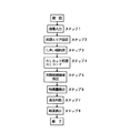
まず、図8のフローチャートに示すように位置決めテーブル31の上に置かれた検査すべきパネル32の蛍光体塗布部33を検査するために照明装置34により照射発光させ、蛍光体の発光をレンズ37を通してカラーテレビカメラ36で撮像しA/D変換後、画像処理部55に入力する(ステップ1)。ここで入力された画像に対して処理する範囲を処理エリアとして設定し(ステップ2)、該処理エリア内の画像データから特定色を抽出し2値化を行い(ステップ3)、面積測定等を行い、該面積等の特徴量を抽出し(ステップ4)、その特徴量の大小により欠陥かどうかの良否判断を行い(ステップ5)、該検出した個々の欠陥をパソコン等のディスプレイにイメージ表示し、その中の欠陥検出位置に欠陥内容を表示する(ステップ6)。
【0009】
【発明が解決しようとする課題】
しかしながら、前記のような検査手段では、通常のカラーカメラを使用しており蛍光体の発光波長を忠実にRGBデータに変換できず、微妙な混色を信頼性高く識別することが困難であった。また、インライン検査に向けた高速検査の実現が困難であった。
【0010】
本発明は上記従来の問題点を解決するもので、PDPの蛍光体の混色検査を信頼性高く、高速に行うプラズマディスプレイ蛍光体の検査装置および検査方法を提供するものである。
【0011】
【課題を解決するための手段】
この目的を達成するために本発明は、蛍光体にこれを発光させる紫外光を照射する照明手段と、蛍光体の発光状態を撮像する撮像手段と、前記撮像手段と前記蛍光体との間に配置され蛍光体の発光特性に合わせた特定の波長の光のみを撮像手段に向け通す複数種類のフィルタとを備え、前記複数種類のフィルタは、580から660nmの波長の光のみを通す第1のフィルタと、500から580nmの波長の光のみを通す第2のフィルタと、400から500nmの波長の光のみを通す第3のフィルタとであり、前記撮像手段は、前記複数種類のフィルタのそれぞれを通過した光を受光することを特徴とする。
【0012】
本発明によれば、蛍光体の発光特性に合わせた所定の波長の光のみを撮像手段に向け通すフィルタを備えているので、蛍光体発光特性に合わせた高感度な光学系を実現することができ、微妙な混色も信頼性高く検出することができる。
【0013】
本発明において、照明手段からの可視光が直接撮像手段に入射しないように可視光カットフィルタを備えるようにすれば、蛍光体の発光色を頼りに検査を行う場合に邪魔になる可視光を低減させることができる。
【0014】
本発明において、照明手段が、光源ランプから放射状に照射されている紫外光を反射により特定距離位置に集光させる反射ミラーを備えるようにすれば、PDPの蛍光体を一定距離からの照明で強く発光させることができる。
【0015】
本発明において、照明手段からの紫外光を蛍光体に照射する箇所の雰囲気の酸素濃度を大気中の濃度より低下させる手段を備えるようにすれば、酸素による紫外光吸収に伴う減衰防止を図り、蛍光体の発光を効率よく行うことができる。
【0018】
【発明の実施の形態】
以下本発明の実施の形態について図1から図6を用いて説明する。
【0019】
図1はプラズマディスプレイ蛍光体検査装置の構成図、図2は同検査装置の検査フロー図である。ここで、検査対象となるプラズマディスプレイパネル(PDP)2の蛍光体塗布部について説明しておく。図3はPDP2の背面の構成図であり、2aは隔壁、2bはガラス基板部、2cはデータ電極部、2dは誘電体層であって、誘電体層2dを備えないものもある。通常は隔壁2aを構成したあと、R(レッド)、G(グリーン)、B(ブルー)の各色の蛍光体3r、3g、3bを隔壁2a内に塗布する。蛍光体3(3r、3g、3bを総称する。)の検査としてはR、G、Bの各蛍光体3が所定の隔壁2a間に欠落やむらがなく、また混色なく塗布されたかどうかを検査する。このような蛍光体3は通常紫外線領域の波長の光を照射すると、一定の色(波長)で発光する。そこで、本検査装置の光学系は、R、G、Bの各蛍光体3の発光励起特性に合わせた波長、たとえば波長220nm〜240nmの紫外光を含む光を照射する照明装置と、該照明により発光された光を撮像するライン状のセンサと、該センサへの受光前に、R、G、B用に特定波長のみを通す3種類のバンドパスフィルタを設けて、各入力信号から画像処理を行い検査を実現する。
【0020】
以下、本実施形態の検査装置の構成について説明する。
【0021】
位置決めテーブル1の上に置かれた検査すべき対象物(PDP)2の蛍光体3の塗布部に紫外光を含む光を照射するために照明装置(照明手段)4が設置される。照明装置4としてはレーザー光から所望の波長のみを取り出したものも考えられる。この照明装置4により発光した光を撮像するために可動テレビカメラ支持部50にレンズ6がセットされライン状のセンサを内蔵するテレビカメラ(撮像手段)5r、5g、5bが3台設置されている。また、該蛍光体3からの発光をテレビカメラ5(5r、5g、5bを総称する。)で撮像する場合に、その光路の途中にR、G、B用の特定波長の光のみを通す3種類のバンドパスフィルタ7r、7g、7b(これらを単に7と称する場合がある。)を各テレビカメラ5の前に設置する。たとえばR用のバンドパスフィルタ7rは580〜660nm、G用のそれ7gは500〜580nm、B用のそれ7bは400〜500nmの範囲の波長の光のみを通す。また図4に示すように、蛍光体発光用の照射光から直接テレビカメラ5に可視光が入射しないように可視光カットフィルタ8を設置すると好適である。また照明照射強度を上げるために蛍光ランプ等の光源ランプ4aと対象物表面までの距離に合わせて、光源ランプ4aから一定距離位置に照明光を集光させる反射ミラー9を照明装置4は備えている。さらに図1に示すように、蛍光体発光用の紫外光の減衰を防ぐために窒素ガス(他の不活性ガスでもよい。)を吹付けて低酸素雰囲気(酸素濃度を大気中の濃度より低下させた雰囲気)とする窒素吹付けノズル10を備えている。テレビカメラ5はテレビカメラ制御手段11により制御れている。テレビカメラ5により入力された映像信号は、アナログディジタル変換(A/D変換)手段12に入り、画像の濃度により0〜255(256階調)等の画像データに数値化され、CPU、ROM、RAM及び入出力等から構成される画像処理部51に入力される。
【0022】
画像処理部51としては、主コントローラあるいは操作盤より指令が与えられる判定制御手段(CPU)13と、処理するエリアを指定する処理エリア設定手段14と、しきい値を決定し欠陥候補領域を抽出する欠陥候補領域抽出手段15と、しきい値を更新する手段16と、該しきい値処理において抽出された1ライン内の線領域の長さ(ランレングス)から欠陥候補領域とノイズを識別するランレングスカット手段17と、候補として残ったランレングスデータや各ランの平均濃度データ(濃度総和データを記憶しても結果的には平均濃度データを記憶することになる。)を記憶する手段18と、ランレングスデータから8近傍処理などにより各領域を認識するラベリング手段19と、個々の欠陥候補領域から面積の大きさ等複数の特徴量を検出する特徴量検出手段20と、該欠陥候補領域特徴量の大小などから候補領域の良否の判断を行う良否判断手段21と、該検出した欠陥をパソコン等のディスプレイ22上に表示する欠陥表示指令手段24とから構成されている。
【0023】
また、上記画像処理部51により検出された欠陥を高倍率のレビューカメラ23により、観察、もしくは自動再検査を行い、その画像を前記ディスプレイ22上に一括表示する指令手段を備えることもある。
【0024】
以上のように構成されたプラズマディスプレイ検査装置について、以下図1、図2、図6を主として参照し、その動作について説明する。
【0025】
位置決めテーブル1の上に置かれたPDP2の蛍光体3の塗布部を連続的に検査するために、テレビカメラ5r、5g、5bを図1のX方向に移動させる。照明装置4からの紫外光の照射によりPDP2のR、G、Bの蛍光体3を発光させ、そのR、G、B光をバンドパスフィルタ5、レンズ6を通して各テレビカメラ5で撮像しA/D変換後、画像処理部51に入力する(図2のステップ1)。ここでRGB用のバンドパスフィルタ7について説明すると、もともと蛍光体の発光特性は図5のR、G、Bに示すようになっており、各蛍光体の発光波長にはオーバーラップする領域が存在する。オーバーラップ領域の波長が各RGB用のセンサで撮像してしまうと微妙な混色が識別できないため、オーバーラップ領域を除外して、検査に有効な波長帯(波線領域)の光のみを通すフィルタにより所望の波長光を得ることが好ましい。例えば、R用のバンドパスフィルタ7rを通して得られた信号7らはRの蛍光体がR以外の蛍光体塗布部へ塗られてしまうものと、R部の蛍光体の欠落、異物付着等を検査する。以下、画像処理について説明する。
【0026】
図6(a)のようにRの蛍光体3rがリブ2aおよびG、B蛍光体3g、3bの塗布部に塗布されてしまった欠陥(R混色)とRの蛍光体3rの塗布部に欠落、異物が存在している様子を示す。このような欠陥を検出するための動作を説明する。
【0027】
テレビカメラ5r、5g、5bをX方向に移動させ、R用のバンドパスフィルタ7rを設けたテレビカメラ5rのライン状のセンサで走査されて入力された画像を、図6(b)に示す。Rの蛍光体3rの塗布部は最高レベル濃度(白)Hとして表われ、G、Bの蛍光体3g、3bの塗布部は最低レベル濃度(黒)Lとして表われる。またレベルは違うが、異物や欠落は低レベル濃度(黒)L1として表われ、Rの蛍光体3rがリブ2aやG、Bの蛍光体3g、3bの塗布部に塗布されてしまった場合は中間レベル濃度(白)Mとして表われる。これらは濃度レベルを示す数値(0〜255)によってデータ処理される。
【0028】
この画像に対して処理する範囲を処理エリアとして設定し(ステップ2)、該処理エリア内のセンサ方向の各素子ごとにしきい値を設定し、しきい値処理を行い各ラインごとランを抽出する(図6(c)、ステップ3)。例えば図6(b)のLで示す各帯状部が含まれる範囲を各処理エリアとして、このエリアにおいて適切なしきい値を設定し、Mに相当する部分をランとして抽出し、又Hで示す各帯状部が含まれる範囲を各処理エリアとして、このエリアにおいて適切なしきい値を設定し、L1に相当する部分をランとし抽出する。ランのデータとしては、各ラインにおいてその始点位置x1 、終点位置x2 のデータすなわちランレングスデータを得る。
【0029】
次に上記のように抽出されたデータをランレングスコードに圧縮する。ランレングスコードに圧縮する場合そのランの長さ(ランレングスデータ)で、ノイズや本来のRの蛍光体塗布部との識別を行い、欠陥候補の絞り込みを行い、不要なデータをカットして高速処理を可能にする。その際、ランレングスデータと共にそのランの平均濃度データを記憶させる(ステップ4)。次にランレングスコードから8近傍等でラベリングを行い欠陥候補領域を抽出する(ステップ5)。個々の欠陥候補領域から複数の特徴量を検出し(ステップ6)、特徴量の大小から良否の判断を行い(ステップ7)、検出した個々の欠陥領域の位置をディスプレイ22に表示する(ステップ8)。好ましくは、その後レビューカメラ23により欠陥画像を高倍率に撮像しディスプレイ22に一括表示して目視確認する。
【0030】
G、Bの蛍光体3g、3bがリブ2aや自身以外の蛍光体塗布領域への塗布混色欠陥についても各々G、B用のバンドパスフィルタ7g、7bを設けたそれぞれの入力系からの画像処理により同様の処理を並列に行い検査する。
【0031】
X方向の走査が終わると、テレビカメラ5r、5g、5bをY方向に所定幅移動させ、次いで再びX方向に移動させることにより、X方向の走査による蛍光体検査を行い、これを繰返してPDP2上の全領域における蛍光体塗布状態の検査を行う。
【0032】
なお、ライン状の受光素子に対し、図6の(b)にHで示す帯状域が直交しておらず、Hで示す帯状域の一部が処理エリアの左右辺のいずれかに交差しているような場合には、この交差している部分のランレングスデータを、不要データとして早めに除去するようにすれば、高速処理を行う上で好適である。また、ライン状の受光素子により撮像した画像データを、一定間隔(例えば10ライン)を隔てた2ライン間の差分画像データに変換して、画像処理を行うようにすれば、PDPの全体的な色調変動の影響を受けずに、局所的な変化を確実にとらえて検査を行うことができる。
【0033】
【発明の効果】
以上のように本発明によれば、蛍光体発光色を感度よく画像化することによって微妙な混色も確実に検査を行うことができる。
【0034】
また本発明によれば、高速処理を実現するプラズマディスプレイ蛍光体検査装置を提供することができる。
【図面の簡単な説明】
【図1】本発明の一実施形態のプラズマディスプレイ蛍光体検査装置の構成図である。
【図2】その動作のフローチャートである。
【図3】PDPの背面の説明図である。
【図4】照明装置の説明図である。
【図5】蛍光体発光特性の説明図である。
【図6】(a)は蛍光体の欠陥の説明図、(b)は入力画像の説明図、(c)は蛍光体欠陥候補領域の圧縮データの説明図である。
【図7】従来例のプラズマディスプレイ蛍光体検査装置の構成図である。
【図8】
従来例の動作のフローチャートである。
【符号の説明】
1 プラズマディスプレイパネル
3 蛍光体
4 照明手段
4a 光源ランプ
5 撮像手段
7 バンドパスフィルタ
8 可視光カットフィルタ
9 反射ミラー
10 窒素吹付けノズル
22 ディスプレイ[0001]
BACKGROUND OF THE INVENTION
The present invention relates to inspection apparatus and method of a plasma display phosphor carried out by checking the image processing of the application state in the phosphor coating process of a plasma display.
[0002]
[Prior art]
Expectations for plasma displays are increasing as large-scale, high-precision displays in the future multimedia era. In the production process, block guarantee in each process has become very important for reducing the loss cost and hence the product cost. Among them, quantitative inspection of mixed colors after applying phosphors for RGB emission is important, and development of high reliability and high-speed inspection in-line is desired for mass production.
[0003]
Hereinafter, an example of the conventional plasma display phosphor inspection described above will be described with reference to FIGS.
[0004]
In order to inspect the phosphor of the plasma display panel (PDP), the
[0005]
The video signal input by the
[0006]
As the
[0007]
The operation of the plasma display phosphor inspection apparatus configured as described above will be described below.
[0008]
First, as shown in the flowchart of FIG. 8, in order to inspect the
[0009]
[Problems to be solved by the invention]
However, in the inspection means as described above, a normal color camera is used, and the emission wavelength of the phosphor cannot be faithfully converted into RGB data, and it is difficult to reliably identify a subtle color mixture. In addition, it has been difficult to realize high-speed inspection for in-line inspection.
[0010]
The present invention is intended to solve the above problems, the color mixture inspection phosphor PDP reliable, there is provided a plasma display phosphor inspection apparatus and method of performing a high speed.
[0011]
[Means for Solving the Problems]
In order to achieve this object, the present invention provides an illumination unit that irradiates a phosphor with ultraviolet light that emits light, an imaging unit that captures an emission state of the phosphor, and a gap between the imaging unit and the phosphor. And a plurality of types of filters that pass only light of a specific wavelength that matches the light emission characteristics of the phosphor to the imaging means, and the plurality of types of filters pass through only light having a wavelength of 580 to 660 nm. a filter, a second filter which passes only light having a wavelength of 580nm to 500, and a third filter for passing only light having a wavelength of 500nm from 400, the imaging unit, each of the plurality of types of filters It is characterized by receiving the passed light .
[0012]
According to the present invention, since the filter for passing only light having a predetermined wavelength according to the light emission characteristic of the phosphor is directed to the imaging means, it is possible to realize a highly sensitive optical system that matches the light emission characteristic of the phosphor. It is possible to detect subtle color mixing with high reliability.
[0013]
In the present invention, if a visible light cut filter is provided so that visible light from the illuminating means does not directly enter the imaging means, visible light that becomes an obstacle when performing an inspection relying on the emission color of the phosphor is reduced. Can be made.
[0014]
In the present invention, if the illuminating means is provided with a reflection mirror for condensing ultraviolet light radiated from the light source lamp at a specific distance position by reflection, the PDP phosphor is strongly illuminated by illumination from a certain distance. Can emit light.
[0015]
In the present invention, if it is provided with means for lowering the oxygen concentration in the atmosphere of the place where the phosphor is irradiated with ultraviolet light from the illumination means than the concentration in the atmosphere, it is intended to prevent attenuation due to absorption of ultraviolet light by oxygen, The phosphor can emit light efficiently.
[0018]
DETAILED DESCRIPTION OF THE INVENTION
Hereinafter, embodiments of the present invention will be described with reference to FIGS.
[0019]
FIG. 1 is a configuration diagram of a plasma display phosphor inspection apparatus, and FIG. 2 is an inspection flow diagram of the inspection apparatus. Here, the phosphor application part of the plasma display panel (PDP) 2 to be inspected will be described. FIG. 3 is a configuration diagram of the back surface of the
[0020]
Hereinafter, the configuration of the inspection apparatus of the present embodiment will be described.
[0021]
An illuminating device (illuminating means) 4 is installed to irradiate the application part of the
[0022]
As the
[0023]
In addition, the defect detected by the
[0024]
The operation of the plasma display inspection apparatus configured as described above will be described with reference mainly to FIGS. 1, 2, and 6.
[0025]
In order to continuously inspect the application portion of the
[0026]
As shown in FIG. 6A, the
[0027]
FIG. 6B shows an image input by scanning the
[0028]
A range to be processed for this image is set as a processing area (step 2), a threshold is set for each element in the sensor direction in the processing area, and threshold processing is performed to extract a run for each line. (FIG. 6C, Step 3). For example, a range including each band-shaped portion indicated by L in FIG. 6B is set as each processing area, an appropriate threshold value is set in this area, a portion corresponding to M is extracted as a run, and each range indicated by H A range including the belt-like portion is set as each processing area, an appropriate threshold value is set in this area, and a portion corresponding to L1 is extracted as a run. As the run data, the data of the start point position x 1 and the end point position x 2 , that is, run length data is obtained for each line.
[0029]
Next, the data extracted as described above is compressed into a run-length code. When compressing to run-length code, the length of the run (run-length data) is used to identify noise and the original R phosphor coating part, narrow down defect candidates, and cut unnecessary data at high speed. Enable processing. At that time, the average density data of the run is stored together with the run length data (step 4). Next, labeling is performed from the run length code in the vicinity of 8 or the like to extract defect candidate areas (step 5). A plurality of feature amounts are detected from the individual defect candidate regions (step 6), the quality is determined based on the size of the feature amounts (step 7), and the positions of the detected individual defect regions are displayed on the display 22 (step 8). ). Preferably, after that, a
[0030]
Image processing from respective input systems in which G and
[0031]
When scanning in the X direction is completed, the
[0032]
Note that the band-shaped area indicated by H in FIG. 6B is not orthogonal to the line-shaped light receiving element, and a part of the band-shaped area indicated by H intersects either the left or right side of the processing area. In such a case, it is preferable to perform the high-speed processing by removing the run length data of the intersecting portion as unnecessary data at an early stage. Further, if image data captured by a line-shaped light receiving element is converted into differential image data between two lines separated by a certain interval (for example, 10 lines) and image processing is performed, the entire PDP is processed. The inspection can be performed by reliably capturing the local change without being affected by the color fluctuation.
[0033]
【The invention's effect】
According to the onset light as described above, it is possible to also reliably inspected subtle color mixing by high sensitivity imaging phosphor emission color.
[0034]
Further, according to the present invention, it is possible to provide a plasma display phosphor inspection apparatus that realizes high-speed processing.
[Brief description of the drawings]
FIG. 1 is a configuration diagram of a plasma display phosphor inspection apparatus according to an embodiment of the present invention.
FIG. 2 is a flowchart of the operation.
FIG. 3 is an explanatory view of the back surface of the PDP.
FIG. 4 is an explanatory diagram of a lighting device.
FIG. 5 is an explanatory diagram of phosphor emission characteristics.
6A is an explanatory diagram of phosphor defects, FIG. 6B is an explanatory diagram of an input image, and FIG. 6C is an explanatory diagram of compressed data of phosphor defect candidate regions;
FIG. 7 is a block diagram of a conventional plasma display phosphor inspection apparatus.
[Fig. 8]
It is a flowchart of operation | movement of a prior art example.
[Explanation of symbols]
DESCRIPTION OF SYMBOLS 1
Claims (8)
Priority Applications (3)
| Application Number | Priority Date | Filing Date | Title |
|---|---|---|---|
| JP31552898A JP3673657B2 (en) | 1998-11-06 | 1998-11-06 | Plasma display phosphor inspection apparatus and inspection method |
| TW089108592A TW451257B (en) | 1998-11-06 | 2000-05-05 | Plasma display phosphor inspecting device |
| US09/629,365 US6697514B1 (en) | 1998-11-06 | 2000-08-01 | Apparatus for inspecting a fluorescent substance on a plasma display |
Applications Claiming Priority (2)
| Application Number | Priority Date | Filing Date | Title |
|---|---|---|---|
| JP31552898A JP3673657B2 (en) | 1998-11-06 | 1998-11-06 | Plasma display phosphor inspection apparatus and inspection method |
| US09/629,365 US6697514B1 (en) | 1998-11-06 | 2000-08-01 | Apparatus for inspecting a fluorescent substance on a plasma display |
Publications (3)
| Publication Number | Publication Date |
|---|---|
| JP2000149781A JP2000149781A (en) | 2000-05-30 |
| JP2000149781A5 JP2000149781A5 (en) | 2005-01-06 |
| JP3673657B2 true JP3673657B2 (en) | 2005-07-20 |
Family
ID=32396163
Family Applications (1)
| Application Number | Title | Priority Date | Filing Date |
|---|---|---|---|
| JP31552898A Expired - Fee Related JP3673657B2 (en) | 1998-11-06 | 1998-11-06 | Plasma display phosphor inspection apparatus and inspection method |
Country Status (3)
| Country | Link |
|---|---|
| US (1) | US6697514B1 (en) |
| JP (1) | JP3673657B2 (en) |
| TW (1) | TW451257B (en) |
Families Citing this family (20)
| Publication number | Priority date | Publication date | Assignee | Title |
|---|---|---|---|---|
| EP1096249B1 (en) * | 1999-10-26 | 2013-05-01 | Hitachi-GE Nuclear Energy, Ltd. | Nondestructive flaw inspection method and apparatus |
| JP4514913B2 (en) * | 2000-07-24 | 2010-07-28 | パナソニック株式会社 | Visual inspection apparatus, visual inspection method and manufacturing apparatus for color display member |
| JP3657930B2 (en) | 2002-07-05 | 2005-06-08 | パイオニアプラズマディスプレイ株式会社 | Plasma display panel manufacturing method, phosphor layer inspection method, and phosphor layer inspection apparatus |
| JP2004085348A (en) * | 2002-08-27 | 2004-03-18 | Dainippon Printing Co Ltd | Inspection apparatus and inspection method for three color patterns |
| KR100925275B1 (en) * | 2002-11-04 | 2009-11-05 | 엘지전자 주식회사 | A phosphor inspector of Plasma Display Panel and the same method |
| KR100541449B1 (en) * | 2003-07-23 | 2006-01-11 | 삼성전자주식회사 | Panel inspection apparatus |
| TW200700799A (en) * | 2005-06-24 | 2007-01-01 | Innolux Display Corp | Testing system of liquid crystal display |
| JP4673151B2 (en) * | 2005-06-30 | 2011-04-20 | 株式会社日立国際電気 | Printing deviation inspection method of phosphor |
| JP4672497B2 (en) * | 2005-09-21 | 2011-04-20 | 株式会社日立国際電気 | Inspection device for phosphor panel |
| US20070128445A1 (en) * | 2005-12-05 | 2007-06-07 | Lear Corporation | Method of making and inspecting an in mold coated article |
| EP1969355B1 (en) * | 2005-12-16 | 2012-04-11 | Automation W+R GmbH | Method and arrangement for detecting material defects in workpieces |
| JP2007265679A (en) * | 2006-03-27 | 2007-10-11 | Hitachi Kokusai Electric Inc | Phosphor inspection device |
| US8111919B2 (en) * | 2008-02-04 | 2012-02-07 | Eyep, Inc. | Feature encoding system and method for connected component labeling |
| JP2008216260A (en) * | 2008-03-18 | 2008-09-18 | Hitachi Kokusai Electric Inc | Phosphor inspection device |
| JP5424660B2 (en) * | 2009-01-23 | 2014-02-26 | 株式会社サキコーポレーション | Inspection device for inspection object |
| JP5424659B2 (en) * | 2009-01-23 | 2014-02-26 | 株式会社サキコーポレーション | Inspection device for inspection object |
| JP2011023638A (en) * | 2009-07-17 | 2011-02-03 | Toshiba Corp | Method of setting inspection area |
| JP2013205055A (en) * | 2012-03-27 | 2013-10-07 | Sinto S-Precision Ltd | Measuring machine |
| KR101472444B1 (en) * | 2012-06-18 | 2014-12-24 | 삼성테크윈 주식회사 | A apparatus for detecting position of phosphor of light emitting diode, a device mounter comprising the apparatus, a method for detecting position of phosphor of light emitting diode, and a lens installation method |
| CN105511122B (en) * | 2015-11-25 | 2019-06-07 | 武汉精测电子集团股份有限公司 | A kind of automatic positioning focusing detection device based on online Machine Vision Detection |
Family Cites Families (8)
| Publication number | Priority date | Publication date | Assignee | Title |
|---|---|---|---|---|
| US4758728A (en) * | 1985-12-24 | 1988-07-19 | Rca Licensing Corporation | Method of measuring mask misregistry in kinescope panel assemblies |
| US5828356A (en) * | 1992-08-21 | 1998-10-27 | Photonics Systems Corporation | Plasma display gray scale drive system and method |
| JPH06260091A (en) * | 1993-03-01 | 1994-09-16 | Mitsubishi Electric Corp | Inspecting method for cathode-ray tube constituting member and device used for its implementation |
| JP3297950B2 (en) * | 1993-07-13 | 2002-07-02 | シャープ株式会社 | Flat panel inspection system |
| US5663569A (en) * | 1993-10-14 | 1997-09-02 | Nikon Corporation | Defect inspection method and apparatus, and defect display method |
| US5928821A (en) * | 1995-12-22 | 1999-07-27 | Thomson Consumer Electronics, Inc. | Method of manufacturing a phosphor screen for a CRT |
| US5790913A (en) * | 1996-10-09 | 1998-08-04 | Thomson Consumer Electronics, Inc. | Method and apparatus for manufacturing a color CRT |
| US5876884A (en) * | 1997-10-02 | 1999-03-02 | Fujitsu Limited | Method of fabricating a flat-panel display device and an apparatus therefore |
-
1998
- 1998-11-06 JP JP31552898A patent/JP3673657B2/en not_active Expired - Fee Related
-
2000
- 2000-05-05 TW TW089108592A patent/TW451257B/en not_active IP Right Cessation
- 2000-08-01 US US09/629,365 patent/US6697514B1/en not_active Expired - Fee Related
Also Published As
| Publication number | Publication date |
|---|---|
| TW451257B (en) | 2001-08-21 |
| US6697514B1 (en) | 2004-02-24 |
| JP2000149781A (en) | 2000-05-30 |
Similar Documents
| Publication | Publication Date | Title |
|---|---|---|
| JP3673657B2 (en) | Plasma display phosphor inspection apparatus and inspection method | |
| EP1943502B1 (en) | Apparatus and methods for inspecting a composite structure for defects | |
| US11300508B2 (en) | Apparatus and method for extracting low intensity photonic signals | |
| JP2006162427A (en) | Method and device for inspecting led chip | |
| JPH08128959A (en) | Optical inspection method and optical inspection device | |
| JP2000149781A5 (en) | ||
| US20050195389A1 (en) | System and method for inspecting electrical circuits utilizing reflective and fluorescent imagery | |
| JP3657930B2 (en) | Plasma display panel manufacturing method, phosphor layer inspection method, and phosphor layer inspection apparatus | |
| JP2002214158A (en) | Defect detecting method and detecting device for transparent plate-like body | |
| KR100723763B1 (en) | Apparatus for inspecting fluorescent material in plasma display | |
| JP4184511B2 (en) | Method and apparatus for defect inspection of metal sample surface | |
| JP2008039444A (en) | Method and apparatus for inspecting foreign matter | |
| JP2008026147A (en) | Inspection device for color filter, and inspection method for the color filter | |
| JP2003240732A (en) | Gold-plated defect-inspecting apparatus | |
| JP4432011B2 (en) | Apparatus and method for inspecting plasma display panel back plate | |
| JPH08304295A (en) | Method and apparatus for detecting surface defect | |
| JP2004117150A (en) | Pattern defect inspection device and pattern defect inspection method | |
| JP2009075044A (en) | Film thickness defective inspection device for conductive polymer layer of organic el panel substrate, and method for inspecting film thickness defective using the same | |
| JP2004146108A (en) | Phosphor inspection method and device | |
| JPH0536795A (en) | Defect inspection apparatus | |
| KR102673099B1 (en) | Inspection Apparatus For Diffuser Panel For Deposition Process | |
| JPH11281588A (en) | Surface inspecting apparatus | |
| JP2007285995A (en) | Defect detecting method, defect detecting apparatus and defect detecting program | |
| JP2007271410A (en) | Flaw detection method, flaw detector, and flaw detection program | |
| JP2007205820A (en) | Inspecting device for color filter, and inspecting method for color filter |
Legal Events
| Date | Code | Title | Description |
|---|---|---|---|
| A521 | Written amendment |
Free format text: JAPANESE INTERMEDIATE CODE: A523 Effective date: 20040213 |
|
| A621 | Written request for application examination |
Free format text: JAPANESE INTERMEDIATE CODE: A621 Effective date: 20040213 |
|
| A977 | Report on retrieval |
Free format text: JAPANESE INTERMEDIATE CODE: A971007 Effective date: 20040928 |
|
| A131 | Notification of reasons for refusal |
Free format text: JAPANESE INTERMEDIATE CODE: A131 Effective date: 20041005 |
|
| A521 | Written amendment |
Free format text: JAPANESE INTERMEDIATE CODE: A523 Effective date: 20041202 |
|
| A131 | Notification of reasons for refusal |
Free format text: JAPANESE INTERMEDIATE CODE: A131 Effective date: 20050118 |
|
| A521 | Written amendment |
Free format text: JAPANESE INTERMEDIATE CODE: A523 Effective date: 20050307 |
|
| TRDD | Decision of grant or rejection written | ||
| A01 | Written decision to grant a patent or to grant a registration (utility model) |
Free format text: JAPANESE INTERMEDIATE CODE: A01 Effective date: 20050412 |
|
| A61 | First payment of annual fees (during grant procedure) |
Free format text: JAPANESE INTERMEDIATE CODE: A61 Effective date: 20050425 |
|
| R150 | Certificate of patent or registration of utility model |
Free format text: JAPANESE INTERMEDIATE CODE: R150 |
|
| FPAY | Renewal fee payment (event date is renewal date of database) |
Free format text: PAYMENT UNTIL: 20080428 Year of fee payment: 3 |
|
| FPAY | Renewal fee payment (event date is renewal date of database) |
Free format text: PAYMENT UNTIL: 20090428 Year of fee payment: 4 |
|
| FPAY | Renewal fee payment (event date is renewal date of database) |
Free format text: PAYMENT UNTIL: 20100428 Year of fee payment: 5 |
|
| FPAY | Renewal fee payment (event date is renewal date of database) |
Free format text: PAYMENT UNTIL: 20110428 Year of fee payment: 6 |
|
| FPAY | Renewal fee payment (event date is renewal date of database) |
Free format text: PAYMENT UNTIL: 20120428 Year of fee payment: 7 |
|
| LAPS | Cancellation because of no payment of annual fees |