JP3671237B2 - Display device - Google Patents
Display device Download PDFInfo
- Publication number
- JP3671237B2 JP3671237B2 JP36856197A JP36856197A JP3671237B2 JP 3671237 B2 JP3671237 B2 JP 3671237B2 JP 36856197 A JP36856197 A JP 36856197A JP 36856197 A JP36856197 A JP 36856197A JP 3671237 B2 JP3671237 B2 JP 3671237B2
- Authority
- JP
- Japan
- Prior art keywords
- wiring
- signal
- drive circuit
- driver
- circuit
- Prior art date
- Legal status (The legal status is an assumption and is not a legal conclusion. Google has not performed a legal analysis and makes no representation as to the accuracy of the status listed.)
- Expired - Fee Related
Links
Images

Landscapes
- Liquid Crystal (AREA)
- Liquid Crystal Display Device Control (AREA)
- Devices For Indicating Variable Information By Combining Individual Elements (AREA)
Description
【0001】
【発明の属する技術分野】
本発明は、映像等を表示する表示装置に関する。
【0002】
【従来の技術】
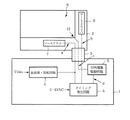
従来の表示装置として、図3〜5に示す液晶表示装置が知られている。この液晶表示装置は、図3に示すように、コントロール基板1とガラス基板2、及びこの両基板1、2に両端部を接続されたFPC(flexible printed circuit)3とを有している。コントロール基板1には、色処理・反転回路4、タイミング発生回路5、及びこのタイミング発生回路5に接続された対向電極駆動回路6が配置されている。
【0003】
ガラス基板2には、ソースドライバ7とゲートドライバ8とがCOG(chip on glass)実装されているとともに、これら両ドライバ7、8により駆動されるTFTパネル9が配置されている。そして、ソースドライバ7は、FPC3を介して色処理・反転回路4とタイミング発生回路5とに接続され、ゲートドライバ8は、FPC3を介してタイミング発生回路5に接続されている。
【0004】
前記TFTパネル9は、図4に示すように、下部のトランジスタ生成基板10とこのトランジスタ生成基板10に対向する対向ガラス基板11とを有している。対向ガラス基板11側に配置されたVCOM(対向電極駆動信号)配線16と、トランジスタ生成基板10側に配置されたCS(コンデンサ駆動信号)配線17とは、接続クロスポイント12にて結合されFPC3を介して対向電極駆駆動回路6に接続されている。
【0005】
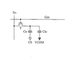
すなわち、TFTパネル9における1画素には、前記両ドライバ7、8からの配線の他に、図5に示すように蓄積コンデンサへの配線CSと対向電極への配線VCOMとが必要であり、一方の配線CSはトランジスタ生成基板10の上面に設けられ、他方の配線VCOMは対向ガラス基板11の下面に設けられる。また、通常VCOMとCSは同一の信号が用いられており、したがって図4をもって前述したように、CS配線17とVCOM配線16とは、接続クロスポイイント12にて結合されている。
【0006】
かかる構成において、色処理・反転回路4は入力されるビデオ信号をRGBの映像データに変換するとともに、反転処理して交流化し、タイミング発生回路5は、同期信号C−SYNCの同期をとって動作し制御信号を生成出力する。これにより、ソースドライバ7には色処理・反転回路4からのRGB信号とタイミング発生回路5からの制御信号とからなるソースドライバ制御信号aが供給され、ゲートドライバ8にはタイミング発生回路からゲートドライバ制御信号bが供給される。また、対向電極駆動回路6には、タイミング発生回路5からVCOM作成用信号dが供給され、これに応答して対向電極駆動回路6は対向電極駆動信号cを生成出力する。この対向電極駆動信号cは、接続クロスポイント12を介してCS配線17とVCOM配線16とに供給されて、コンデンサ駆動信号CS及び対向電極駆動信号VCOMとして機能する。
【0007】
【発明が解決しようとする課題】
しかしながら、かかる従来の液晶表示装置にあっては、図3に示したように、両ドライバ7、8とタイミング発生回路5とが別のLSIで構成されているとともに、タイミング発生回路5がコントロール基板1に配置され、両ドライバ7、8がガラス基板2に配置されている。したがって、コントロール基板1には、タイミング発生回路5を構成するタイミング発生LSI等の実装面積が必要となり、その結果基板が大型化してしまう。
【0008】
また、コントロール基板1とガラス基板2との間に、FPC3を介して多数の制御信号線を接続する必要がある。すなわち、コントロール基板1からFPC3を介してガラス基板2上に入力される信号は、前記ソースドライバ制御信号aとして、少なくともクロック信号MCLK、スタート信号SRT、クリア信号CLR、出力イネーブルOE、及び各映像信号R,G,Bの7種であり、まずは7本の信号線が必要となる。また、ゲートドライバ制御信号bとして、ゲートクロックGPCK、ゲートスタート信号GSRT、ゲート出力イネーブルGRESの3種であり、3本の信号線が必要となる。さらに、対向電極駆動信号(VCOM)d用の信号線も必要となることから、少なくとも計11本の信号線が必要となる。したがって、かかる多数の信号線の配線が不可欠となることにより、製造工程の長大化及びコスト増を招いてしまう。
【0009】
さらに、これらコントロール基板1側から多数の制御信号が、該コントロール基板1、FPC3及びガラス基板2上の配線で引き回されることから、遅延量が信号間でばらついてしまい、その結果、液晶表示装置の表示性能が劣化し、場合によっては誤作動が生じてしまう。
【0010】
本発明は、このような従来の課題に鑑みてなされたものであり、制御基板を小型化し得るととも製造工程の短縮化とコストの低減を図ることができ、さらには表示性能の向上を図ることのできる表示装置を提供することを目的とするものである。
【0011】
【課題を解決するための手段】
前記課題を解決するために請求項1記載の発明にあっては、所定のタイミングで動作するドライブ回路と、このドライブ回路により駆動されて表示動作する表示パネルとを備えた表示装置において、前記ドライブ回路の動作タイミングを制御する制御手段を当該ドライブ回路に設け、前記ドライブ回路は、前記表示パネルの走査線を駆動するゲートドライバと信号線を駆動するソースドライバとで構成され、いずれか一方のドライバに前記制御手段を設けるとともに、他方のドライバに該制御手段からの制御信号を供給するようにしたものである。したがって、他の回路からドライブ回路にその動作タイミングを制御するための制御信号を供給する必要がなく、該制御信号を供給するための配線が不要となるとともに、他の回路の規模を縮小し得る。
【0012】
また、請求項2記載の発明にあっては、所定のタイミングで動作するドライブ回路と、このドライブ回路により駆動されて表示動作する表示パネルとを備え、前記ドライブ回路が前記表示パネルの構成部材に配置された表示装置において、前記表示パネルの構成部材に、前記ドライブ回路の動作タイミングを制御する制御手段を設け、前記ドライブ回路は、前記表示パネルの走査線を駆動するゲートドライバと信号線を駆動するソースドライバとで構成され、いずれか一方のドライバに前記制御手段を設けるとともに、他方のドライバに該制御手段からの制御信号を供給するようにしたものである。したがって、他の回路から表示パネルの構成部材にドライブ回路の動作タイミングを制御するための制御信号を供給する必要がなく、該制御信号を供給するための配線が不要となるとともに、他の回路の規模を縮小し得る。
【0016】
【発明の実施の形態】
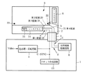
以下、本発明の実施の形態を図に従って説明する。すなわち、本実施の形態にかかる液晶表示装置は、図1に示すように、コントロール基板1とガラス基板2、及びこの両基板1、2に両端部を接続されたFPC3とを有している。コントロール基板1には、ビデオ信号を映像データに変換し反転処理する色処理・反転回路4、所定周波数のクロック信号を生成出力するクロック作成回路13、及び対向電極駆動回路6が配置されている。
【0017】
ガラス基板2には、ソースドライバ14とゲートドライバ8とがCOG実装されているとともに、これら両ドライバ8、14により駆動されるTFTパネル9が配置されている。また、ソースドライバ14には、タイミング発生回路(TG)15が内蔵されている。そして、ソースドライバ14は、第1配線18にて、FPC3を介して、色処理・反転回路4とクロック作成回路13とに接続されているとともに、第2配線19にて対向電極駆動回路6に接続されている。
【0018】
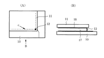
前記TFTパネル9は、図2に示すように、下部のトランジスタ生成基板10とこのトランジスタ生成基板10に対向する上部の対向ガラス基板11とを有している。この対向ガラス基板11の下面には、VCOM(対向電極駆動信号)配線16が配設され、トランジスタ生成基板10の上面には、CS(コンデンサ駆動信号)配線17と第3配線20、及び第4配線21が配設されている。
【0019】
VCOM配線16の一端部16aは、トランジスタ生成基板10の上面から立ち上がる第1接続クロスポイント22にて、前記第4配線21及びFPC3を介して対向電極駆動回路6に接続されている。また、VCOM配線16の他端部16bは、対向ガラス基板11の下面から立ち下がる第2接続クロスポイント21にて、CS配線17の対応する他端部17bに接続されている。さらに、前記第3配線22は、その一端部がソースドライバ14に他端部がゲートドライバ8に各々接続されている。
【0020】
かかる構成において、色処理・反転回路4は入力されるビデオ信号をRGBの映像データに変換するとともに、反転処理して交流化する。この交流化された映像データRGBと同期信号C−SYNC、及びクロック作成回路13から生成されたクロック信号とは、第1配線18よりソースドライバ制御信号aとしソースドライバ14に供給される。
【0021】
すると、ソースドライバ7がこのソースドライバ制御信号aに基づき動作するとともに、内蔵されているタイミング発生回路15が動作し、ソースドライバ14からは、第2配線19を介して対向電極駆動回路6にVCOM作成用信号dが供給され、かつ第3配線20を介してゲートドライバ8にゲートドライバ制御信号bが供給される。
【0022】
前記VCOM作成用信号dが供給されると、対向電極駆動回路6はこれに応答して、対向電極駆動信号cを生成出力する。この対向電極駆動信号cは、第1接続クロスポイント22を介してCS配線17に供給された後、第2接続クロスポイント23介してVCOM配線16とに供給されて、コンデンサ駆動信号CS及び対向電極駆動信号VCOMとして機能する。
【0023】
ここで、タイミング発生回路15は、ガラス基板2側のソースドライバ14に内蔵されていることから、従来のようにコントロール基板1にタイミング発生LSIを配置する必要はない。よって、コントロール基板1にこれらの実装面積を確保する必要がなく、その結果基板を小型化して撮像装置の小型化を促進することができる。
【0024】
また、タイミング発生回路15がガラス基板2側に配置されることから、コントロール基板1とガラス基板2との間に必要な制御信号線が減少する。すなわち、コントロール基板1からFPC3を介してガラス基板2上に入力される信号としては、色処理・反転回路4からの各映像信号R,G,B、クロック作成回路13からのクロック入力CK,同期信号C−SYNC,VCOM作成用信号FRP(信号d),及び対向電極駆動信号VCOM(信号c)の7種であり計7本の信号線があればよい。よって、コントロール基板1とガラス基板2との間に必要な制御信号線が減少し、これに伴って、製造工程の短縮化及びコストの低減を図ることができる。
【0025】
しかも、図2(B)に明示したように、対向電極駆動回路6に接続される第4配線21を、第1接続クロスポイント22にてVCOM配線16の一端部16aに接続し、VCOM配線16の他端部16bを、第2接続クロスポイント23にてCS配線17の対応する他端部17bに接続させるようにした。よって、ソースドライバ14とゲートドライバ8とを接続する第3配線20を設けても、この第3配線20が同一平面上でCS配線17と交差することはない。
【0026】
つまり、図4(B)に示した従来構造において、ソースドライバ14とゲートドライバ8とを接続する第3配線20を設けたとすると、この第3配線20がトランジスタ生成基板10上でCS配線17と平面交差することとなる。したがって、両者を一層で配線することができず、多層にする必要が生ずるとともに、多層にした場合には信号間のクロストークにより、表示性能が劣化し、場合によっては誤作動が生ずる。
【0027】
しかし、前述のように本実施の形態によれば、ソースドライバ14とゲートドライバ8とを接続する第3配線20を設けても、この第3配線20が同一平面上でCS配線17と交差することはないことから、多層にする必要はなく、よって、クロストークによる表示性能の劣化や誤作動が生ずることもない。したがって、トランジスタ生成基板10上にソースドライバ14とゲートドライバ8とを接続する第3配線20を設けつつ、クロストークによる表示性能の劣化や誤作動を未然に防止することが可能となる。
【0028】
【発明の効果】
以上説明したように本発明は、表示パネルを駆動するドライブ回路の動作タイミングを制御する制御手段を当該ドライブ回路に設け、あるいはドライブ回路が配置された表示パネルの構成部材に、該ドライブ回路の動作タイミングを制御する制御手段を設けるようにした。よって、表示パネルを制御するコントロール基板への実装部品及び実装面積を減少させてその小型化を図ることができるとともに、コントロール基板と表示パネル間に配線される信号線の数を減少させることができる。よって、製造工程の短縮化及びコストの低減を図ることができるのみならず、ドライブ回路の制御信号が遅延したり、遅延量が信号間でばらついてしまうこともなく、表示装置の表示性能を向上させることができる。
【0029】
また、ゲートドライバとソースドライバのいずれか一方に制御手段を設けるとともに、他方のドライバに該制御手段からの制御信号を供給するようにした。よって、コントロール基板から両ドライバの動作タイミングを制御するたの制御信号を供給せずとも、両ドライバを精度よく所定の動作タイミングで動作させることができ、製造工程の短縮化及びコストの低減を図りつつ、表示装置の表示性能を向上させることができる。
【0032】
【図面の簡単な説明】
【図1】本発明の一実施の形態を示すブロック回路図である。
【図2】(A)はTFTパネルの平面図、(B)は(A)のB矢示図である。
【図3】従来の表示装置を示すブロック図である。
【図4】(A)は同表示装置におけるTFTパネルの平面図、(B)は(A)のB矢示図である。
【図5】同表示装置における1画素の回路図である。
【符号の説明】
8 ゲートドライバ
9 TFTパネル
14 ソースドライバ
15 タイミング発生器[0001]
BACKGROUND OF THE INVENTION
The present invention relates to a display device that displays video and the like.
[0002]
[Prior art]
A liquid crystal display device shown in FIGS. 3 to 5 is known as a conventional display device. As shown in FIG. 3, the liquid crystal display device includes a control substrate 1, a
[0003]
A source driver 7 and a
[0004]
As shown in FIG. 4, the
[0005]
That is, one pixel in the
[0006]
In such a configuration, the color processing / inversion circuit 4 converts the input video signal into RGB video data and inverts it into an alternating current, and the
[0007]
[Problems to be solved by the invention]
However, in such a conventional liquid crystal display device, as shown in FIG. 3, both the
[0008]
Further, it is necessary to connect a large number of control signal lines between the control substrate 1 and the
[0009]
Further, since a large number of control signals are routed from the control board 1 side by wiring on the control board 1, the
[0010]
The present invention has been made in view of such a conventional problem. The control board can be miniaturized, the manufacturing process can be shortened, the cost can be reduced, and the display performance can be improved. It is an object of the present invention to provide a display device that can be used.
[0011]
[Means for Solving the Problems]
In order to solve the above-mentioned problem, in the first aspect of the present invention, in the display device including a drive circuit that operates at a predetermined timing and a display panel that is driven by the drive circuit and performs a display operation, the drive Control means for controlling the operation timing of the circuit is provided in the drive circuit, and the drive circuit includes a gate driver that drives the scanning lines of the display panel and a source driver that drives the signal lines. Is provided with the control means, and the control signal from the control means is supplied to the other driver. Therefore, it is not necessary to supply a control signal for controlling the operation timing from another circuit to the drive circuit, wiring for supplying the control signal becomes unnecessary, and the scale of the other circuit can be reduced. .
[0012]
According to a second aspect of the present invention, a drive circuit that operates at a predetermined timing and a display panel that is driven by the drive circuit and performs a display operation are provided, and the drive circuit is a constituent member of the display panel. In the arranged display device, a control means for controlling an operation timing of the drive circuit is provided in a component of the display panel, and the drive circuit drives a gate driver and a signal line for driving a scanning line of the display panel. The control means is provided in one of the drivers, and the control signal from the control means is supplied to the other driver. Therefore, it is not necessary to supply a control signal for controlling the operation timing of the drive circuit from other circuits to the constituent members of the display panel, and wiring for supplying the control signals is not necessary. The scale can be reduced.
[0016]
DETAILED DESCRIPTION OF THE INVENTION
Hereinafter, embodiments of the present invention will be described with reference to the drawings. That is, the liquid crystal display device according to the present embodiment includes a control substrate 1, a
[0017]
On the
[0018]
As shown in FIG. 2, the
[0019]
One
[0020]
In such a configuration, the color processing / inversion circuit 4 converts an input video signal into RGB video data, and inverts it to convert it into an alternating current. The AC video data RGB, the synchronization signal C-SYNC, and the clock signal generated from the
[0021]
Then, the source driver 7 operates based on the source driver control signal a, and the built-in
[0022]
When the VCOM creation signal d is supplied, the counter
[0023]
Here, since the
[0024]
Further, since the
[0025]
In addition, as clearly shown in FIG. 2B, the fourth wiring 21 connected to the counter
[0026]
That is, in the conventional structure shown in FIG. 4B, if the third wiring 20 for connecting the
[0027]
However, according to the present embodiment as described above, even if the third wiring 20 that connects the
[0028]
【The invention's effect】
As described above, according to the present invention, the control means for controlling the operation timing of the drive circuit for driving the display panel is provided in the drive circuit, or the operation of the drive circuit is provided in the constituent member of the display panel in which the drive circuit is arranged. A control means for controlling the timing is provided. Therefore, it is possible to reduce the size by reducing the mounting parts and the mounting area on the control board for controlling the display panel, and it is possible to reduce the number of signal lines wired between the control board and the display panel. . Therefore, not only can the manufacturing process be shortened and the cost can be reduced, but also the display performance of the display device can be improved without delaying the control signal of the drive circuit or the delay amount varying between the signals. Can be made.
[0029]
Further, the control means is provided in one of the gate driver and the source driver, and the control signal from the control means is supplied to the other driver. Therefore, both drivers can be accurately operated at a predetermined operation timing without supplying a control signal for controlling the operation timing of both drivers from the control board, thereby shortening the manufacturing process and reducing the cost. However, the display performance of the display device can be improved.
[0032]
[Brief description of the drawings]
FIG. 1 is a block circuit diagram showing an embodiment of the present invention.
2A is a plan view of a TFT panel, and FIG. 2B is a view as indicated by an arrow B in FIG.
FIG. 3 is a block diagram illustrating a conventional display device.
4A is a plan view of a TFT panel in the display device, and FIG. 4B is a view as indicated by an arrow B in FIG.
FIG. 5 is a circuit diagram of one pixel in the display device.
[Explanation of symbols]
8
Claims (2)
前記ドライブ回路の動作タイミングを制御する制御手段を、当該ドライブ回路に設け、
前記ドライブ回路は、前記表示パネルの走査線を駆動するゲートドライバと信号線を駆動するソースドライバとで構成され、いずれか一方のドライバに前記制御手段を設けるとともに、他方のドライバに該制御手段からの制御信号を供給するようにしたことを特徴とする表示装置。In a display device including a drive circuit that operates at a predetermined timing and a display panel that is driven by the drive circuit and performs a display operation,
Control means for controlling the operation timing of the drive circuit is provided in the drive circuit ,
The drive circuit includes a gate driver that drives a scanning line of the display panel and a source driver that drives a signal line, and the driver is provided with the control means, and the other driver is provided with the control means. A display device characterized in that a control signal is supplied .
前記表示パネルの構成部材に、前記ドライブ回路の動作タイミングを制御する制御手段を設け、
前記ドライブ回路は、前記表示パネルの走査線を駆動するゲートドライバと信号線を駆動するソースドライバとで構成され、いずれか一方のドライバに前記制御手段を設けるとともに、他方のドライバに該制御手段からの制御信号を供給するようにしたことを特徴とする表示装置。In a display device comprising: a drive circuit that operates at a predetermined timing; and a display panel that is driven by the drive circuit to perform a display operation, and the drive circuit is disposed in a component of the display panel.
A control means for controlling the operation timing of the drive circuit is provided on a component of the display panel ,
The drive circuit includes a gate driver that drives a scanning line of the display panel and a source driver that drives a signal line, and the driver is provided with the control means, and the other driver is provided with the control means. A display device characterized in that a control signal is supplied .
Priority Applications (1)
| Application Number | Priority Date | Filing Date | Title |
|---|---|---|---|
| JP36856197A JP3671237B2 (en) | 1997-12-26 | 1997-12-26 | Display device |
Applications Claiming Priority (1)
| Application Number | Priority Date | Filing Date | Title |
|---|---|---|---|
| JP36856197A JP3671237B2 (en) | 1997-12-26 | 1997-12-26 | Display device |
Related Child Applications (1)
| Application Number | Title | Priority Date | Filing Date |
|---|---|---|---|
| JP2005042132A Division JP4111197B2 (en) | 2005-02-18 | 2005-02-18 | Display device |
Publications (2)
| Publication Number | Publication Date |
|---|---|
| JPH11194713A JPH11194713A (en) | 1999-07-21 |
| JP3671237B2 true JP3671237B2 (en) | 2005-07-13 |
Family
ID=18492148
Family Applications (1)
| Application Number | Title | Priority Date | Filing Date |
|---|---|---|---|
| JP36856197A Expired - Fee Related JP3671237B2 (en) | 1997-12-26 | 1997-12-26 | Display device |
Country Status (1)
| Country | Link |
|---|---|
| JP (1) | JP3671237B2 (en) |
Families Citing this family (10)
| Publication number | Priority date | Publication date | Assignee | Title |
|---|---|---|---|---|
| JP3618086B2 (en) | 2000-07-24 | 2005-02-09 | シャープ株式会社 | Multiple column electrode drive circuit and display device |
| US7098901B2 (en) | 2000-07-24 | 2006-08-29 | Sharp Kabushiki Kaisha | Display device and driver |
| KR100511349B1 (en) * | 2001-12-29 | 2005-08-31 | 엘지.필립스 엘시디 주식회사 | Liquid crystal display device |
| KR100787916B1 (en) * | 2002-03-11 | 2007-12-24 | 삼성전자주식회사 | Liquid crystal display |
| TWI331743B (en) * | 2005-03-11 | 2010-10-11 | Chimei Innolux Corp | Driving system in a liquid crystal display |
| TWI304563B (en) * | 2005-03-11 | 2008-12-21 | Himax Tech Inc | Apparatus and method for generating gate control signals of lcd |
| TWI292569B (en) | 2005-03-11 | 2008-01-11 | Himax Tech Ltd | Chip-on-glass liquid crystal display and transmission method thereof |
| CN100416349C (en) * | 2005-03-31 | 2008-09-03 | 奇景光电股份有限公司 | Liquid crystal display adopting chip on glass package and data transmission method thereof |
| CN100388350C (en) * | 2005-03-31 | 2008-05-14 | 奇景光电股份有限公司 | Apparatus and method for generating gate control signal of liquid crystal display |
| KR101117736B1 (en) | 2010-02-05 | 2012-02-27 | 삼성모바일디스플레이주식회사 | Display apparatus |
-
1997
- 1997-12-26 JP JP36856197A patent/JP3671237B2/en not_active Expired - Fee Related
Also Published As
| Publication number | Publication date |
|---|---|
| JPH11194713A (en) | 1999-07-21 |
Similar Documents
| Publication | Publication Date | Title |
|---|---|---|
| US8373636B2 (en) | Driving method for display device | |
| US8174662B2 (en) | Display circuits | |
| US20030043100A1 (en) | Liquid crystal display and driving method thereof | |
| JP2004062201A (en) | Liquid crystal display device without gate PCB and FPC | |
| JP4550334B2 (en) | Liquid crystal display device and method of manufacturing liquid crystal display device | |
| JP3638123B2 (en) | Display module | |
| US20030030604A1 (en) | Liquid crystal display | |
| CN103366666A (en) | Display driving framework and signal transmission method thereof, display device and manufacturing method thereof | |
| JP3671237B2 (en) | Display device | |
| CN1940658B (en) | Liquid crystal display and manufacturing method thereof | |
| TW505804B (en) | Liquid crystal display device | |
| JP2004109969A (en) | Liquid crystal display | |
| JP3811398B2 (en) | Liquid crystal display device and flexible substrate | |
| JP3593392B2 (en) | Liquid crystal display | |
| JP3875806B2 (en) | Liquid crystal display | |
| JP4111197B2 (en) | Display device | |
| JP2012042567A (en) | Liquid crystal display and liquid crystal module | |
| JPH04333095A (en) | Semiconductor device | |
| JP2001022287A (en) | Flat panel display | |
| KR20010073679A (en) | Liquid Crystal Display Module with Separate Control Printed Circuit Boards | |
| KR101174779B1 (en) | Liquid crystal displayl device of line on glass type | |
| KR101001421B1 (en) | LCD Display | |
| KR20060000113A (en) | LCD and its driving method | |
| JPH043025A (en) | Display panel connection structure | |
| JPH0854638A (en) | Liquid crystal display device |
Legal Events
| Date | Code | Title | Description |
|---|---|---|---|
| A977 | Report on retrieval |
Free format text: JAPANESE INTERMEDIATE CODE: A971007 Effective date: 20041203 |
|
| A131 | Notification of reasons for refusal |
Free format text: JAPANESE INTERMEDIATE CODE: A131 Effective date: 20041221 |
|
| A521 | Written amendment |
Free format text: JAPANESE INTERMEDIATE CODE: A523 Effective date: 20050218 |
|
| TRDD | Decision of grant or rejection written | ||
| A01 | Written decision to grant a patent or to grant a registration (utility model) |
Free format text: JAPANESE INTERMEDIATE CODE: A01 Effective date: 20050315 |
|
| A61 | First payment of annual fees (during grant procedure) |
Free format text: JAPANESE INTERMEDIATE CODE: A61 Effective date: 20050328 |
|
| R150 | Certificate of patent or registration of utility model |
Free format text: JAPANESE INTERMEDIATE CODE: R150 |
|
| FPAY | Renewal fee payment (event date is renewal date of database) |
Free format text: PAYMENT UNTIL: 20090428 Year of fee payment: 4 |
|
| FPAY | Renewal fee payment (event date is renewal date of database) |
Free format text: PAYMENT UNTIL: 20090428 Year of fee payment: 4 |
|
| FPAY | Renewal fee payment (event date is renewal date of database) |
Free format text: PAYMENT UNTIL: 20100428 Year of fee payment: 5 |
|
| FPAY | Renewal fee payment (event date is renewal date of database) |
Free format text: PAYMENT UNTIL: 20110428 Year of fee payment: 6 |
|
| FPAY | Renewal fee payment (event date is renewal date of database) |
Free format text: PAYMENT UNTIL: 20120428 Year of fee payment: 7 |
|
| FPAY | Renewal fee payment (event date is renewal date of database) |
Free format text: PAYMENT UNTIL: 20120428 Year of fee payment: 7 |
|
| FPAY | Renewal fee payment (event date is renewal date of database) |
Free format text: PAYMENT UNTIL: 20130428 Year of fee payment: 8 |
|
| FPAY | Renewal fee payment (event date is renewal date of database) |
Free format text: PAYMENT UNTIL: 20130428 Year of fee payment: 8 |
|
| FPAY | Renewal fee payment (event date is renewal date of database) |
Free format text: PAYMENT UNTIL: 20140428 Year of fee payment: 9 |
|
| LAPS | Cancellation because of no payment of annual fees |