JP3661925B2 - Video signal processing circuit and method for display device - Google Patents
Video signal processing circuit and method for display device Download PDFInfo
- Publication number
- JP3661925B2 JP3661925B2 JP29497099A JP29497099A JP3661925B2 JP 3661925 B2 JP3661925 B2 JP 3661925B2 JP 29497099 A JP29497099 A JP 29497099A JP 29497099 A JP29497099 A JP 29497099A JP 3661925 B2 JP3661925 B2 JP 3661925B2
- Authority
- JP
- Japan
- Prior art keywords
- saturation
- gradation
- video signal
- level
- region
- Prior art date
- Legal status (The legal status is an assumption and is not a legal conclusion. Google has not performed a legal analysis and makes no representation as to the accuracy of the status listed.)
- Expired - Fee Related
Links
- 238000012545 processing Methods 0.000 title claims description 44
- 238000000034 method Methods 0.000 title claims description 20
- 230000009467 reduction Effects 0.000 claims description 143
- 238000003672 processing method Methods 0.000 claims description 9
- 230000008569 process Effects 0.000 claims description 5
- 230000007423 decrease Effects 0.000 claims description 3
- 238000012937 correction Methods 0.000 description 21
- 238000010586 diagram Methods 0.000 description 20
- 239000011159 matrix material Substances 0.000 description 14
- 230000003044 adaptive effect Effects 0.000 description 12
- 230000007274 generation of a signal involved in cell-cell signaling Effects 0.000 description 12
- 238000009792 diffusion process Methods 0.000 description 7
- 230000008859 change Effects 0.000 description 2
- 238000006243 chemical reaction Methods 0.000 description 2
- 230000006872 improvement Effects 0.000 description 2
- 230000004048 modification Effects 0.000 description 2
- 238000012986 modification Methods 0.000 description 2
- 230000000737 periodic effect Effects 0.000 description 2
- 238000013459 approach Methods 0.000 description 1
- 230000001934 delay Effects 0.000 description 1
- 230000003111 delayed effect Effects 0.000 description 1
- 238000001514 detection method Methods 0.000 description 1
- 230000000694 effects Effects 0.000 description 1
- 238000005401 electroluminescence Methods 0.000 description 1
- 238000009499 grossing Methods 0.000 description 1
- 230000001771 impaired effect Effects 0.000 description 1
- 230000000007 visual effect Effects 0.000 description 1
Images
Landscapes
- Transforming Electric Information Into Light Information (AREA)
- Video Image Reproduction Devices For Color Tv Systems (AREA)
- Processing Of Color Television Signals (AREA)
- Control Of Indicators Other Than Cathode Ray Tubes (AREA)
Description
【0001】
【発明の属する技術分野】
本発明は、表示装置に用いる映像信号処理回路及び方法に係り、特に、プラズマディスプレイパネル表示装置(PDP),フィールドエミッションディスプレイ装置(FED),デジタルマイクロミラーデバイス(DMD),エレクトロルミネッセンスディスプレイ(EL)等のように、デジタル的に限られた中間階調しか表現することができない表示装置において、特定の階調領域、例えば低階調領域である暗部の画像における画質を向上させるのに好適な表示装置の映像信号処理回路及び方法に関する。
【0002】
【従来の技術】
映像信号を表示する表示装置の内、例えば、1フィールドを複数のサブフィールドに分割して階調表示するPDPや、パルス幅変調(PWM)によって階調表示するFED、さらにはDMD等のマトリクス型表示装置においては、駆動方法によってはデジタル的に制限された階調数でしか映像を表現することができない。
【0003】
通常、受像機を陰極線管(CRT)と想定しているテレビジョン放送等では、予め、送信機側でガンマ特性を施しており、受像機側のCRTが有する逆ガンマ特性と合わせてリニアな階調特性となるようにしている。しかしながら、デジタル的に制限された階調数で画像表示する上記のようなマトリクス型表示装置においては、CRTとは異なり、表示装置自体はリニアな階調特性である。従って、普段見慣れているCRTによる表示装置と同様な階調特性で画像表示するには、表示装置の入力映像信号に2.2乗の逆ガンマ補正処理を施し、リニアな階調特性に戻して画像表示することが必要である。
【0004】
【発明が解決しようとする課題】
ところで、例えばデジタル変換したR(赤),G(緑),B(青)の各映像信号に逆ガンマ補正を施して、上記のようなマトリクス型表示装置に画像表示すると、特に、低輝度領域における階調数が損なわれ、階調の連続性がなくなる。特に、表示装置がPDPの場合では、1フィールドを発光量の重み付けの異なる複数のサブフィールドによって構成し、そのサブフィールドを複数選択することによって階調を表現する。従って、低輝度領域では、階調ステップ毎の輝度差が大きいため、映像信号が単色の場合でも混合色の場合でも、隣接階調に対する視覚的な彩度の変化が大きくなってしまう。その結果、色の疑似輪郭状の画質妨害が発生したり、デジタルのビット落ちのような彩度の画像となってしまうという問題点があった。
【0005】
この種の現象は、特に、暗く平坦な彩度の画像が続く場合等において顕著に現れてしまう。この現象に対して、ディザや誤差拡散法等の多階調化処理を施して、黒付近の低階調領域の彩度変化を滑らかにするという改善方法があるが、静止画像を表示したとき、逆に、黒付近の暗部画像において周期的な色のパターンノイズとして認識される画質妨害を招いてしまうという問題点があった。
【0006】
また、上述した問題点の他の改善方法として、例えば特開平9−198000号公報に記載のように、低輝度領域における彩度を低減する方法がある。しかしながら、上記公報に記載の方法では、低輝度領域における彩度を一律に低減してしまうので、低輝度領域において彩度が大きい画像に対しても彩度が落ちた画像となってしまい、違和感のある画像となってしまうという問題点があった。
【0007】
なお、上述した問題点は、黒付近の低階調領域のみならず、サブフィールドの選択状況によっては、部分的に中間階調領域や高階調領域においても発生することがあり、効果的な改善策が望まれていた。
【0008】
本発明はこれらの問題点に鑑みなされたものであり、低階調領域等の特定の階調領域において色の疑似輪郭状の画質妨害が発生したり、ビット落ちのような彩度の画像となってしまったり、色のパターンノイズが発生することを抑制することができ、良好な色再現表示を行うことができる表示装置の映像信号処理回路及び方法を提供することを目的とする。
【0009】
【課題を解決するための手段】
本発明は、上述した従来の技術の課題を解決するため、
(1)表示装置に入力する映像信号を処理する表示装置の映像信号処理回路において、前記映像信号の彩度レベルを低減させる彩度低減量を可変するための制御信号である彩度低減制御信号を発生する彩度低減制御信号発生手段と、前記彩度低減制御信号に基づいて、前記彩度低減量を示す三角形状の波形信号を発生する彩度低減量発生手段と、前記映像信号の予め設定した所定の彩度レベルの領域内における彩度レベルから前記三角形状の波形信号を減算して前記映像信号の彩度レベルを低減させる彩度レベル低減手段とを備えて構成したことを特徴とする表示装置の映像信号処理回路を提供し、
(2)表示装置に入力する映像信号を処理する表示装置の映像信号処理方法において、前記映像信号の彩度レベルを低減させる彩度低減量を可変するための制御信号である彩度低減制御信号を発生し、前記彩度低減制御信号に基づいて、前記彩度低減量を示す三角形状の波形信号を発生し、前記映像信号の予め設定した所定の彩度レベルの領域内における彩度レベルから前記三角形状の波形信号を減算して前記映像信号の彩度レベルを低減させることを特徴とする表示装置の映像信号処理方法を提供するものである。
【0010】
【発明の実施の形態】
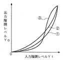
以下、本発明の表示装置の映像信号処理回路及び方法について、添付図面を参照して説明する。図1は本発明の映像信号処理回路及び方法を用いる表示装置の一構成例を示すブロック図、図2は本発明の映像信号処理回路及び方法の一実施例である図1中の映像信号処理回路1の具体的構成例を示すブロック図、図3は図2中の適応型彩度低減回路12の具体的構成例を示すブロック図、図4は図3中の彩度低減制御信号発生回路122が発生する彩度低減制御信号の一例を示す特性図、図5は図3中の彩度低減量発生回路123,124が発生する彩度低減量の一例を示す特性図、図6及び図7は本発明の一実施例による彩度低減動作を示す特性図、図8は本発明の一実施例による彩度低減動作の変形例を示す特性図、図9は図1中の逆ガンマ補正回路2に設定する逆ガンマ補正特性の例を示す特性図、図10は図3中の彩度低減制御信号発生回路122が発生する彩度低減制御信号の他の一例を示す特性図、図11は本発明の他の実施例による彩度低減動作を示す特性図である。
【0011】
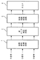
図1に示す本実施例では、デジタル的に制限された階調数でしか映像を表現することができないマトリクス型表示装置として、PDPを用いた場合について示している。勿論、本発明の表示装置としては、PDPに限定されるものではない。図1において、R,G,B信号よりなる3系統の映像信号は、映像信号処理回路1に入力される。映像信号処理回路1は、これらの映像信号に対して、本発明の映像信号処理方法を含む各種の映像信号処理を施し、逆ガンマ補正回路2に入力する。R,G,B信号は一例として8ビットのデジタル信号、即ち、256階調の信号である。本発明となる映像信号処理回路1の具体的構成及び動作は後に詳述する。
【0012】
逆ガンマ補正処理回路2は、入力されたR,G,B信号に対し、それぞれ同じ特性の逆ガンマ補正処理を施し、一例として12ビットのデジタル信号、即ち、4096階調の信号として出力する。8ビットのデジタル信号を12ビットのデジタル信号として出力するのは、逆ガンマ補正処理によって階調数が損なわれるのを防ぐためである。逆ガンマ補正回路2より出力されたR,G,B信号は、誤差拡散処理回路3に入力される。
【0013】
誤差拡散処理回路3は、入力されたR,G,B信号に対し、それぞれ同じ特性の誤差拡散処理を施して出力する。即ち、12ビットのデジタル信号の内の例えば下位4ビットを誤差ビットとして隣接画素に対して所定の比率で拡散し、結果として上位8ビットのデジタル信号として出力する。誤差拡散処理回路3によって誤差拡散処理されたR,G,B信号はPDP4に入力される。PDP4は、サブフィールド処理等の駆動回路処理を施した上で、画面上にR,G,B信号を画像表示する。
【0014】
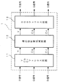
ここで、図2及び図3を用いて図1中の映像信号処理回路1の具体的構成及び動作について説明する。図2に示すように、映像信号処理回路1は、YCbCrマトリクス回路11,適応型彩度低減回路12,RGBマトリクス回路13を備えている。入力されたR,G,B信号は、YCbCrマトリクス回路11に入力される。YCbCrマトリクス回路11は、入力されたR,G,B信号に対して、YCbCrマトリクス変換処理を施すことにより、輝度(Y)信号と2つの色差(Cb,Cr)信号を出力する。Y,Cb,Cr信号は適応型彩度低減回路12に入力される。なお、色差信号の形式は入力された映像信号の方式によって異なり、ハイビジョン信号であればPb,Pr信号である。よって、YPbPrマトリクス回路の場合もある。
【0015】
適応型彩度低減回路12は、Y信号の値、即ち、輝度に応じて、Cb,Cr信号の値、即ち、彩度を適応的に低減して出力する。適応型彩度低減回路12の具体的構成及び動作は後に詳述する。RGBマトリクス回路13は、適応型彩度低減回路12より出力されたY,Cb,Cr信号に対して、RGBマトリクス変換処理を施すことにより、再びR,G,B信号に戻して出力する。
【0016】
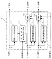
次に、図3を用いて適応型彩度低減回路12の具体的構成及び動作について説明する。図3において、Y信号は階調レベル判定回路121に入力され、Cb,Cr信号はそれぞれ彩度低減量発生回路123,124に入力される。なお、ここでは簡略化のためY信号がそのまま適応型彩度低減回路12より出力されるように図示しているが、実際には、後述するCb,Cr信号に対する信号処理による遅延分と合わせるため、遅延回路によってY信号を遅延させ、Y信号とCb,Cr信号とのタイミングを合わせる。
【0017】
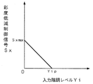
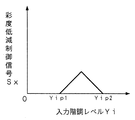
階調レベル判定回路121は、入力されたY信号の階調レベルを判定(検出)し、その判定出力を彩度低減制御信号発生回路122に入力する。彩度低減制御信号発生回路122は、図4に示すように、入力階調レベルYiにおける予め設定した所定の階調Yip以下において、彩度低減制御信号Sxを発生する。彩度低減制御信号Sxは、階調Yipから階調0に向かうに従って順次大きくなっており、この例では、階調レベルYiと彩度低減制御信号Sxとは直線の関係となっている。階調0で彩度低減制御信号Sxは最大値Sxmaxである。階調Yip以下における階調レベルYiと彩度低減制御信号Sxとの関係は直線に限定されることはなく、曲線であってもよい。入力階調レベルYiが小さくなるに従って、彩度低減制御信号Sxが大きくなればよい。なお、彩度低減制御信号発生回路122には、どのような彩度低減制御信号Sxを発生させるかを制御する制御信号が入力される。これについては後述する。
【0018】
彩度低減制御信号発生回路122より出力された彩度低減制御信号Sxは彩度低減量発生回路123,124に入力される。彩度低減量発生回路123,124の回路構成は同一であり、同じ動作をする。彩度低減量発生回路123,124は、入力された彩度低減制御信号Sxに基づいて、Cb,Cr信号の彩度レベルを適応的に低減するための彩度低減量Xを発生する。なお、彩度低減量発生回路123,124にCb,Cr信号を入力しているのは、彩度低減量Xを決定する際、入力されたCb,Cr信号に基づいて(例えば、入力されたCb,Cr信号に所定の係数を乗じることによって)彩度低減量Xを得るためである。勿論、彩度低減量発生回路123,124にCb,Cr信号を入力せず、彩度低減量Xを発生するよう構成することも可能である。
【0019】
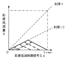
彩度低減量発生回路123,124は、入力された彩度低減制御信号Sxに基づいて、次のようにして実際にCb,Cr信号より低減する彩度レベル(彩度低減量X)を決定する。図5において、横軸を彩度低減制御信号Sx、縦軸を彩度低減量発生回路123,124が発生する彩度低減量Xとする。図5に示すように、彩度低減量発生回路123,124は、彩度低減制御信号Sxに応じて三角形状の彩度低減量Xを発生する。この例では、入力されたCb,Cr信号に対する利得を1/2とし、横軸と利得1/2の線とで挟まれる範囲において、三角形状の彩度低減量Xを決定するようにしている。彩度低減量Xは、斜線で示すように、三角形の面積で表され、彩度低減制御信号Sxが大きくなれば、その三角形の面積が矢印で示すように順次大きくなっていく。入力されたCb,Cr信号に対する利得は1/2に限定されることはなく、利得1であってもよく、利得1/2未満であってもよく、適宜設定すればよい。
【0020】
減算器125,126には、それぞれ、Cb,Cr信号と彩度低減量発生回路123,124より出力された彩度低減量Xが入力される。減算器125,126は、Cb,Cr信号より彩度低減量Xを減算して出力する。なお、ここでも簡略化のためCb,Cr信号がそのまま減算器125,126に入力されるように図示しているが、実際には、彩度低減量発生回路123,124におけるCb,Cr信号に対する信号処理による遅延分と合わせるため、遅延回路によってCb,Cr信号を遅延させ、彩度低減量発生回路123,124を経ていないCb,Cr信号と彩度低減量発生回路123,124より出力される彩度低減量Xとのタイミングを合わせる。減算器125,126には、Cb,Cr信号よりどのようにして彩度低減量Xを減算するかを制御する制御信号が入力される。これについては後述する。
【0021】
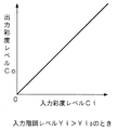
以上の動作をまとめると次のようになる。まず、入力階調レベルYiが所定の階調Yipを超える場合には、Cb,Cr信号における入力彩度レベルCiはそのまま出力彩度レベルCoとして適応型彩度低減回路12より出力される。即ち、適応型彩度低減回路12における彩度低減量Xは0であるので、入力彩度レベルCiと出力彩度レベルCoとの関係は図6に示す如くとなる。なお、所定の階調Yipとは一例として256階調の場合で64階調程度である。
【0022】
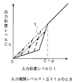
一方、入力階調レベルYiが所定の階調Yip以下の場合には、彩度低減制御信号発生回路122が階調レベルYiに基づいて図4で説明したような彩度低減制御信号Sxを発生し、彩度低減量発生回路123,124が彩度低減制御信号Sxに基づいて適応的に彩度低減量Xを発生する。そして、減算器125,126が入力されたCb,Cr信号よりその彩度低減量Xを減算するので、入力彩度レベルCiと出力彩度レベルCoとの関係は図7に示す如くとなる。図5に示すように彩度低減量Xが増加すれば、図7に矢印で示すように、入力彩度レベルCiと出力彩度レベルCoとの関係も変化していく。
【0023】
即ち、図7において、破線で示す直線tは彩度低減量Xが0である場合の特性に相当し、図5に示す彩度低減量Xの面積が減算されるので、入力彩度レベルCiと出力彩度レベルCoとの特性は、図7に示すように直線tの下方に落ち込むような特性となる。なお、図5に斜線で示す三角形の面積と図7に斜線で示す直線tからの削除部分の三角形の面積とは同一である。図5に示すように彩度低減量Xが斜線で示す状態から矢印で示すように増加すれば、図7に示す入力彩度レベルCiと出力彩度レベルCoとの特性においても、矢印で示すように削除部分の面積が順次大きくなっていく。
【0024】
以上のように、図4〜図7に示す実施例では、入力階調レベルYiが予め設定した階調Yip以下である低階調領域において、入力彩度レベルCiが予め設定した入力彩度レベルCip以下の場合に対して、入力彩度レベルCiを入力彩度レベルCiが0である無彩色側から低減し、入力階調レベルYiが0に近づくにつれて、入力彩度レベルCiの低減量を増大するように適応的に制御している。従って、特に、黒付近の暗部画像において発生する色の疑似輪郭状の画質妨害が抑制され、ビット落ちのような彩度の画像となることも抑制される。また、多階調化処理による周期的な色のパターンノイズの発生が抑制されると共に、低輝度部において彩度が大きい画像に対しては彩度が落ちないので、暗部でも良好な色再現表示を行うことができる。
【0025】
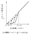
図7に示す実施例では、入力彩度レベルCiが予め設定した彩度レベルCip以下の場合に対して、出力彩度レベルCoが0とならない程度に低減するようにしたが、無彩色側の彩度低減を重点的に行う場合には、減算する彩度低減量Xの開始位置を図7よりも入力彩度レベルCiに対して低彩度方向にシフトすることにより、図8に示すように、入力彩度レベルCi0以下の入力彩度レベルCiでは出力彩度レベルCoを0にするようにしてもよい。なお、この場合、入力彩度レベルCiを低減する最大の入力彩度レベルCiは、図7に示す入力彩度レベルCipよりも低彩度方向にシフトしたCip′となる。
【0026】
以上の実施例においては、彩度低減を行う階調レベル領域を階調Yip以下である低階調領域としたが、これに限定されるものではない。彩度低減を行う階調レベル領域を、必要に応じて、中間階調領域や高階調領域としても効果的である。例えば、PDPの場合では、サブフィールドの選択状況により隣接階調間で発光輝度が大きく異なる階調領域に対して彩度低減を行う階調レベル領域を設定しても効果的に作用する。また、実際に彩度低減を行う彩度レベル領域についても同様に、無彩色付近から重点的に彩度低減しても効果的であるし、場合によっては中間彩度領域や高彩度領域を中心に彩度低減を行っても効果的である。
【0027】
図1における逆ガンマ補正回路2に設定する逆ガンマ補正特性は、図9の特性▲1▼〜▲3▼に示すように、種々異なる場合がある。また、逆ガンマ補正特性を入力信号等に応じて種々切り換える場合がある。なお、図9の横軸である入力階調レベルYiは、逆ガンマ補正回路2の入力階調レベルであり、縦軸である出力階調レベルYoは、逆ガンマ補正回路2の出力階調レベルである。逆ガンマ補正特性を切り換える場合には、中間階調領域もしくは高階調領域における低彩度領域や中間彩度領域もしくは高彩度領域において、色の疑似輪郭状の画質妨害が発生したり、ビット落ちのような彩度の画像となる場合がある。このような場合には、彩度低減を行う階調レベル領域を中間階調領域もしくは高階調領域とし、彩度低減を行う彩度レベル領域を低彩度領域や中間彩度領域もしくは高彩度領域とすると効果的である。
【0028】
図10は、彩度低減を行う階調レベル領域を中間階調領域に設定した場合の例を示している。図3中の彩度低減制御信号発生回路122は、図10に示すように、入力階調レベルYiが階調Yip1〜Yip2の範囲である中間階調領域において、三角形状に彩度低減制御信号Sxを発生する。彩度低減量発生回路123,124は、この彩度低減制御信号Sxを基にして彩度低減量Xを発生する。そして、減算器125,126は、入力されたCb,Cr信号の低彩度領域と中間彩度領域と高彩度領域のいずれかの彩度レベル領域において彩度低減量Xを減算して彩度を低減する。
【0029】
彩度低減制御信号発生回路122が図4に示すように階調Yip以下である低階調領域において彩度低減制御信号Sxを発生するのか、図10に示すように階調Yip1〜Yip2の範囲である中間階調領域において彩度低減制御信号Sxを発生するのか、さらには、特に図示しないが、高階調領域において彩度低減制御信号Sxを発生するのかを切換制御するのが、上述した彩度低減制御信号発生回路122に入力する制御信号の働きである。また、この制御信号によっていかなる特性の彩度低減制御信号Sxを発生するのかを切り換えることも可能である。
【0030】
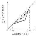
図11は、彩度低減を行う彩度レベル領域を中間彩度領域に設定した場合の例を示している。図4に示すように階調Yip以下である低階調領域において彩度低減制御信号Sxを発生させたり、図10に示すように階調Yip1〜Yip2の範囲である中間階調領域において彩度低減制御信号Sxを発生させたり、高階調領域において彩度低減制御信号Sxを発生させ、彩度低減量発生回路123,124が彩度低減量Xを発生する。そして、減算器125,126は、入力されたCb,Cr信号の入力彩度レベルCiがCip1〜Cip2の範囲である中間彩度領域において彩度低減量Xを減算して彩度を低減する。
【0031】
減算器125,126が図7に示すように低彩度領域において彩度低減量Xを減算して彩度を低減するのか、図11に示すように中間彩度領域において彩度低減量Xを減算して彩度を低減するのか、さらには、特に図示しないが、高彩度領域において彩度低減量Xを減算して彩度を低減するのかを切換制御するのが、上述した減算器125,126に入力する制御信号の働きである。また、この制御信号によって低彩度領域,中間彩度領域,高彩度領域においてどのように彩度を低減するかを切り換えることも可能である。厳密には、中間彩度領域や高彩度領域において彩度を低減する場合には、彩度低減量Xの値を変更する必要がある。彩度低減量発生回路123,124や減算器125,126において彩度低減量Xの値を変更すればよい。
【0032】
さらに、図11に破線の矢印で示すように、入力彩度レベルCiを中間彩度領域における高彩度側の入力彩度レベルCip2側から低減するようにしてもよい。なお、減算器125,126に入力する制御信号は、Cb,Cr信号のビット数と同じビット数(図3の例では8ビット)とする。
【0033】
以上のように、彩度低減する際の階調レベル領域と、実際に彩度を低減する彩度レベル領域とは、表示装置が有する表示特性等によってもたらされる画質妨害が発生する領域や画像内容、または、逆ガンマ補正特性等によって、適宜設定すればよい。具体的には、次の組み合わせが考えられる。図4〜図8に示す実施例のように、低階調領域において低彩度領域の彩度を低減する。低階調領域において中間彩度領域の彩度を低減する。低階調領域において高彩度領域の彩度を低減する。中間階調領域において低彩度領域の彩度を低減する。中間階調領域において中間彩度領域の彩度を低減する。中間調領域において高彩度領域の彩度を低減する。高階調領域において低彩度領域の彩度を低減する。高階調領域において中間彩度領域の彩度を低減する。高階調領域において高彩度領域の彩度を低減する。
【0034】
なお、低階調領域とは、階調0から任意の中間階調レベルまでの領域を意味する。そして、通常、この中間階調レベルは、最大階調よりも階調0に近い階調レベルである。中間階調領域とは、階調0より離れた任意の第1の中間階調レベルから任意の第2の中間階調レベルまでの領域を意味する。中間階調領域とは、中央階調領域に限定されるものではない。高階調領域とは、階調0より離れた任意の中間階調レベルから最大階調までの領域を意味する。そして、通常、この中間階調レベルは、階調0よりも最大階調に近い階調レベルである。
【0035】
同様に、低彩度領域とは、彩度0から任意の中間彩度レベルまでの領域を意味する。そして、通常、この中間彩度レベルは、最大彩度よりも彩度0に近い彩度レベルである。中間彩度領域とは、彩度0より離れた任意の第1の中間彩度レベルから任意の第2の中間彩度レベルまでの領域を意味する。中間彩度領域とは、中央彩度領域に限定されるものではない。高彩度領域とは、彩度0より離れた任意の中間彩度レベルから最大彩度までの領域を意味する。そして、通常、この中間彩度レベルは、彩度0よりも最大彩度に近い彩度レベルである。
【0036】
さらに、彩度を適応的に低減する場合、図7及び図11に実線の矢印で示すように、入力彩度レベルCiが低い側、即ち、図7の例では無彩色(彩度0)側から、図11の例では入力彩度レベルCip1側から低減することが好ましいが、表示装置が有する表示特性等によってもたらされる画質妨害が発生する領域や画像内容、または、逆ガンマ補正特性等によって、どの方向から彩度を低減するかは適宜設定すればよい。
【0037】
以上説明した本発明の表示装置の映像信号処理回路及び方法は、入力された映像信号に逆ガンマ補正処理を施してリニアな階調特性に戻して画像表示を行うような、デジタル的に限られた中間階調しか表現することができない表示装置の暗部や特定の中間もしくは高階調領域における画質を向上させるのに極めて好適であるが、他の表示装置に対して用いてもよい。ビデオ画像表示やパソコン表示モニタ用のCRT表示装置、または、投写型の表示装置に用いても効果的に作用する。
【0038】
【発明の効果】
以上詳細に説明したように、本発明の表示装置の映像信号処理回路及び方法によれば、低階調領域等の特定の階調領域において色の疑似輪郭状の画質妨害が発生したり、ビット落ちのような彩度の画像となってしまったり、色のパターンノイズが発生することを極めて効果的に抑制することができ、良好な色再現表示を行うことが可能となる。
【図面の簡単な説明】
【図1】本発明を用いる表示装置の一構成例を示すブロック図である。
【図2】本発明の一実施例である図1中の映像信号処理回路1の具体的構成例を示すブロック図である。
【図3】図2中の適応型彩度低減回路12の具体的構成例を示すブロック図である。
【図4】図3中の彩度低減制御信号発生回路122が発生する彩度低減制御信号の一例を示す特性図である。
【図5】図3中の彩度低減量発生回路123,124が発生する彩度低減量の一例を示す特性図である。
【図6】本発明の一実施例による彩度低減動作を示す特性図である。
【図7】本発明の一実施例による彩度低減動作を示す特性図である。
【図8】本発明の一実施例による彩度低減動作の変形例を示す特性図である。
【図9】図1中の逆ガンマ補正回路2に設定する逆ガンマ補正特性の例を示す特性図である。
【図10】図3中の彩度低減制御信号発生回路122が発生する彩度低減制御信号の他の一例を示す特性図である。
【図11】本発明の他の実施例による彩度低減動作を示す特性図である。
【符号の説明】
1 映像信号処理回路
2 逆ガンマ補正回路
3 誤差拡散処理回路
4 プラズマディスプレイパネル表示装置(PDP)
11 YCbCrマトリクス回路
12 適応型彩度低減回路
13 RGBマトリクス回路
121 階調レベル判定回路(階調レベル検出手段)
122 彩度低減制御信号発生回路
123,124 彩度低減量発生回路
125,126 減算器(彩度レベル低減手段)[0001]
BACKGROUND OF THE INVENTION
The present invention relates to a video signal processing circuit and method used for a display device, and more particularly, to a plasma display panel display device (PDP), a field emission display device (FED), a digital micromirror device (DMD), and an electroluminescence display (EL). In a display device that can express only a limited intermediate gradation in a digital manner, a display suitable for improving the image quality in an image of a specific gradation area, for example, a dark area that is a low gradation area. The present invention relates to a video signal processing circuit and method of an apparatus.
[0002]
[Prior art]
Among display devices that display video signals, for example, a PDP that displays gradation by dividing one field into a plurality of subfields, an FED that displays gradation by pulse width modulation (PWM), and a matrix type such as DMD In a display device, an image can be expressed only with a digitally limited number of gradations depending on the driving method.
[0003]
Normally, in television broadcasting and the like where the receiver is assumed to be a cathode ray tube (CRT), a gamma characteristic is given in advance on the transmitter side, and a linear scale is combined with the inverse gamma characteristic of the CRT on the receiver side. It is designed to have a tonal characteristic. However, in the above-described matrix display device that displays an image with a digitally limited number of gradations, unlike the CRT, the display device itself has linear gradation characteristics. Therefore, in order to display an image with the same gradation characteristics as a display device using CRT that is usually used, the input image signal of the display device is subjected to a 2.2 power inverse gamma correction process to return to the linear gradation characteristics. It is necessary to display an image.
[0004]
[Problems to be solved by the invention]
By the way, for example, when inverse gamma correction is performed on digitally converted R (red), G (green), and B (blue) video signals and an image is displayed on the matrix display device as described above, the low-luminance region in particular is displayed. In this case, the number of gradations is impaired, and gradation continuity is lost. In particular, when the display device is a PDP, one field is composed of a plurality of subfields with different light emission weights, and gradation is expressed by selecting a plurality of subfields. Therefore, in the low luminance region, since the luminance difference for each gradation step is large, the change in the visual saturation with respect to the adjacent gradation becomes large regardless of whether the video signal is a single color or a mixed color. As a result, there has been a problem that the image quality disturbance in the form of a pseudo contour of color occurs or the image has a saturation like a digital bit drop.
[0005]
This type of phenomenon is particularly noticeable when a dark and flat chroma image continues. For this phenomenon, there is an improvement method of smoothing the saturation change in the low gradation area near black by applying multi-gradation processing such as dithering and error diffusion method, but when displaying a still image On the contrary, there is a problem in that the image quality interference is recognized as the periodic color pattern noise in the dark part image near black.
[0006]
As another method for improving the above-described problems, there is a method for reducing the saturation in the low luminance region as described in JP-A-9-198000, for example. However, in the method described in the above publication, the saturation in the low luminance region is uniformly reduced, so that an image with a low saturation is obtained even for an image having a high saturation in the low luminance region. There was a problem that it became an image with.
[0007]
Note that the above-described problem may occur not only in the low gradation region near black but also in the intermediate gradation region and the high gradation region depending on the selection condition of the subfield, which is an effective improvement. A plan was desired.
[0008]
The present invention has been made in view of these problems, and an image quality disturbance such as a pseudo-contour color of a color occurs in a specific gradation region such as a low gradation region or an image having a saturation such as a bit drop. It is an object of the present invention to provide a video signal processing circuit and a method for a display device that can suppress the occurrence of color noise and the generation of color pattern noise and can perform good color reproduction display.
[0009]
[Means for Solving the Problems]
The present invention solves the above-mentioned problems of the prior art,
(1) In a video signal processing circuit of a display device that processes a video signal input to the display device, Based on the saturation reduction control signal, a saturation reduction control signal generating means for generating a saturation reduction control signal that is a control signal for varying a saturation reduction amount for reducing the saturation level of the video signal, Saturation reduction amount generating means for generating a triangular waveform signal indicating the saturation reduction amount, and the triangular waveform signal from a saturation level in a predetermined saturation level region of the video signal. Subtract the saturation level of the video signal Providing a video signal processing circuit of a display device characterized by comprising a saturation level reduction means for reducing,
(2) In a video signal processing method of a display device for processing a video signal input to the display device, A saturation reduction control signal, which is a control signal for changing the saturation reduction amount for reducing the saturation level of the video signal, is generated, and the saturation reduction amount is indicated based on the saturation reduction control signal. Generating a waveform signal having a shape, and subtracting the triangular waveform signal from a saturation level in a predetermined saturation level region of the video signal to obtain a saturation level of the video signal. It is an object of the present invention to provide a video signal processing method for a display device, which is characterized by being reduced.
[0010]
DETAILED DESCRIPTION OF THE INVENTION
Hereinafter, a video signal processing circuit and method of a display device according to the present invention will be described with reference to the accompanying drawings. FIG. 1 is a block diagram showing a configuration example of a display device using the video signal processing circuit and method of the present invention, and FIG. 2 is a video signal processing in FIG. 1 which is an embodiment of the video signal processing circuit and method of the present invention. 3 is a block diagram showing a specific configuration example of the
[0011]
In this embodiment shown in FIG. 1, a case is shown in which a PDP is used as a matrix type display device that can express an image only with a digitally limited number of gradations. Of course, the display device of the present invention is not limited to the PDP. In FIG. 1, three systems of video signals composed of R, G, and B signals are input to the video
[0012]
The inverse gamma
[0013]
The error
[0014]
Here, the specific configuration and operation of the video
[0015]
The adaptive saturation reduction circuit 12 adaptively reduces and outputs the value of the Cb and Cr signals, that is, the saturation, according to the value of the Y signal, that is, the luminance. The specific configuration and operation of the adaptive saturation reduction circuit 12 will be described in detail later. The RGB matrix circuit 13 performs an RGB matrix conversion process on the Y, Cb, and Cr signals output from the adaptive saturation reduction circuit 12, thereby returning the signals to the R, G, and B signals again.
[0016]
Next, a specific configuration and operation of the adaptive saturation reduction circuit 12 will be described with reference to FIG. In FIG. 3, the Y signal is input to the gradation
[0017]
The gradation
[0018]
The saturation reduction control signal Sx output from the saturation reduction control
[0019]
Based on the input saturation reduction control signal Sx, the saturation reduction
[0020]
The
[0021]
The above operation is summarized as follows. First, when the input gradation level Yi exceeds the predetermined gradation Yip, the input saturation level Ci in the Cb and Cr signals is output as it is from the adaptive saturation reduction circuit 12 as the output saturation level Co. That is, since the saturation reduction amount X in the adaptive saturation reduction circuit 12 is 0, the input saturation level C The relationship between i and the output saturation level Co is as shown in FIG. The predetermined gradation Yip is, for example, about 256 gradations in the case of 256 gradations.
[0022]
On the other hand, when the input gradation level Yi is equal to or lower than the predetermined gradation Yip, the saturation reduction control
[0023]
That is, in FIG. 7, a straight line t indicated by a broken line corresponds to a characteristic when the saturation reduction amount X is 0, and the area of the saturation reduction amount X shown in FIG. And the output saturation level Co are characteristics that fall below the straight line t as shown in FIG. Note that the area of the triangle indicated by the oblique lines in FIG. 5 is the same as the area of the triangle in the deleted portion from the straight line t indicated by the oblique lines in FIG. As shown in FIG. 5, if the saturation reduction amount X increases from the state shown by the oblique lines as shown by the arrows, the characteristics of the input saturation level Ci and the output saturation level Co shown in FIG. As can be seen, the area of the deleted portion increases gradually.
[0024]
As described above, in the embodiments shown in FIGS. 4 to 7, the input saturation level Ci is set in advance in the low gradation region where the input gradation level Yi is equal to or lower than the preset gradation Yip. In the case of Cip or less, the input saturation level Ci is reduced from the achromatic color side where the input saturation level Ci is 0, and as the input gradation level Yi approaches 0, the reduction amount of the input saturation level Ci is reduced. It is adaptively controlled to increase. Therefore, in particular, the pseudo-contour image quality disturbance of the color that occurs in the dark part image near black is suppressed, and the saturation of the image such as bit dropping is also suppressed. In addition, generation of periodic color pattern noise due to multi-gradation processing is suppressed, and saturation does not drop for images with high saturation in low-brightness areas. It can be performed.
[0025]
In the embodiment shown in FIG. 7, the output saturation level Co is reduced to a level that does not become 0 when the input saturation level Ci is equal to or lower than the preset saturation level Cip. In the case where saturation reduction is to be focused on, the start position of the saturation reduction amount X to be subtracted is shifted in the lower saturation direction with respect to the input saturation level Ci than in FIG. In addition, the output saturation level Co may be set to 0 at the input saturation level Ci that is equal to or lower than the input saturation level Ci0. In this case, the maximum input saturation level Ci for reducing the input saturation level Ci is Cip ′ shifted in the lower saturation direction than the input saturation level Cip shown in FIG.
[0026]
In the above embodiment, the gradation level region for reducing the saturation is the low gradation region having the gradation Yip or less, but is not limited to this. The gradation level region for reducing the saturation is also effective as an intermediate gradation region or a high gradation region as necessary. For example, in the case of the PDP, even if a gradation level region for reducing the saturation is set for a gradation region in which the light emission luminance is greatly different between adjacent gradations depending on the selection condition of the subfield, it effectively works. Similarly, in the saturation level area where the saturation is actually reduced, it is also effective to reduce the saturation mainly from the vicinity of the achromatic color, and depending on the case, the intermediate saturation area and the high saturation area may be the center. It is also effective to reduce the saturation.
[0027]
The inverse gamma correction characteristics set in the inverse
[0028]
FIG. 10 shows an example in which the gradation level region for reducing the saturation is set to the intermediate gradation region. As shown in FIG. 10, the saturation reduction control
[0029]
Whether the saturation reduction control
[0030]
FIG. 11 shows an example in which the saturation level region for performing saturation reduction is set to the intermediate saturation region. As shown in FIG. 4, the saturation reduction control signal Sx is generated in the low gradation region below the gradation Yip, or the saturation is generated in the intermediate gradation region that is in the range of the gradations Yip1 to Yip2 as shown in FIG. The reduction control signal Sx is generated or the saturation reduction control signal Sx is generated in the high gradation region, and the saturation reduction
[0031]
Whether the
[0032]
Furthermore, as indicated by the dashed arrows in FIG. 11, the input saturation level Ci may be reduced from the input saturation level Cip2 side on the high saturation side in the intermediate saturation region. Note that the control signal input to the
[0033]
As described above, the gradation level region for reducing the saturation and the saturation level region for actually reducing the saturation are the regions and image contents in which the image quality interference caused by the display characteristics of the display device occurs. Alternatively, it may be set as appropriate according to the inverse gamma correction characteristic or the like. Specifically, the following combinations are possible. As in the embodiment shown in FIGS. 4 to 8, the saturation of the low saturation region is reduced in the low gradation region. The saturation of the intermediate saturation area is reduced in the low gradation area. The saturation of the high saturation area is reduced in the low gradation area. The saturation of the low saturation region is reduced in the intermediate gradation region. The saturation of the intermediate saturation area is reduced in the intermediate gradation area. In the halftone area, the saturation of the high saturation area is reduced. The saturation of the low saturation region is reduced in the high gradation region. The saturation of the intermediate saturation area is reduced in the high gradation area. The saturation of the high saturation area is reduced in the high gradation area.
[0034]
Note that the low gradation region means a region from
[0035]
Similarly, the low saturation region means a region from
[0036]
Further, when the saturation is adaptively reduced, as shown by solid line arrows in FIGS. 7 and 11, the input saturation level Ci is low, that is, the achromatic color (saturation 0) side in the example of FIG. Therefore, in the example of FIG. 11, it is preferable to reduce from the input saturation level Cip1 side. However, depending on the region where the image quality interference is caused by the display characteristics of the display device, the image content, or the inverse gamma correction characteristics, The direction from which saturation is reduced may be set as appropriate.
[0037]
The video signal processing circuit and method of the display device according to the present invention described above are digitally limited such that an input video signal is subjected to inverse gamma correction processing to return to linear gradation characteristics and image display is performed. The present invention is extremely suitable for improving the image quality in a dark part of a display device that can express only intermediate gradations or in a specific intermediate or high gradation region, but may be used for other display devices. Even when used in a CRT display device for video image display or personal computer display monitor, or a projection display device, it works effectively.
[0038]
【The invention's effect】
As described in detail above, the video signal processing circuit and method of the display device of the present invention According to In a specific gradation area such as a low gradation area, a color pseudo-contour image quality disturbance, a saturation image such as a bit drop, or color pattern noise may occur. It can be suppressed extremely effectively, and good color reproduction display can be performed.
[Brief description of the drawings]
FIG. 1 is a block diagram illustrating a configuration example of a display device using the present invention.
FIG. 2 is a block diagram showing a specific configuration example of the video
FIG. 3 is a block diagram illustrating a specific configuration example of an adaptive saturation reduction circuit 12 in FIG. 2;
4 is a characteristic diagram illustrating an example of a saturation reduction control signal generated by a saturation reduction control
FIG. 5 is a characteristic diagram illustrating an example of a saturation reduction amount generated by the saturation reduction
FIG. 6 is a characteristic diagram illustrating a saturation reduction operation according to an embodiment of the present invention.
FIG. 7 is a characteristic diagram illustrating a saturation reduction operation according to an embodiment of the present invention.
FIG. 8 is a characteristic diagram showing a modification of the saturation reduction operation according to the embodiment of the present invention.
FIG. 9 is a characteristic diagram showing an example of reverse gamma correction characteristics set in the reverse
10 is a characteristic diagram showing another example of the saturation reduction control signal generated by the saturation reduction control
FIG. 11 is a characteristic diagram illustrating a saturation reduction operation according to another embodiment of the present invention.
[Explanation of symbols]
1 Video signal processing circuit
2 Inverse gamma correction circuit
3 Error diffusion processing circuit
4 Plasma display panel display (PDP)
11 YCbCr matrix circuit
12 Adaptive saturation reduction circuit
13 RGB matrix circuit
121 gradation level determination circuit (gradation level detection means)
122 Saturation Reduction Control Signal Generation Circuit
123, 124 Saturation reduction amount generation circuit
125, 126 subtractor (saturation level reduction means)
Claims (8)
前記映像信号の彩度レベルを低減させる彩度低減量を可変するための制御信号である彩度低減制御信号を発生する彩度低減制御信号発生手段と、
前記彩度低減制御信号に基づいて、前記彩度低減量を示す三角形状の波形信号を発生する彩度低減量発生手段と、
前記映像信号の予め設定した所定の彩度レベルの領域内における彩度レベルから前記三角形状の波形信号を減算して前記映像信号の彩度レベルを低減させる彩度レベル低減手段とを備えて構成したことを特徴とする表示装置の映像信号処理回路。In a video signal processing circuit of a display device that processes a video signal input to the display device,
A saturation reduction control signal generating means for generating a saturation reduction control signal that is a control signal for varying a saturation reduction amount for reducing the saturation level of the video signal;
A saturation reduction amount generating means for generating a triangular waveform signal indicating the saturation reduction amount based on the saturation reduction control signal;
Saturation level reduction means for reducing the saturation level of the video signal by subtracting the triangular waveform signal from the saturation level within a predetermined saturation level region of the video signal A video signal processing circuit for a display device.
前記彩度低減制御信号発生手段は、予め設定した所定の階調レベルの領域内でのみ前記彩度低減制御信号を発生することを特徴とする請求項1記載の表示装置の映像信号処理回路。 A gradation level detecting means for detecting a gradation level of the video signal;
2. The video signal processing circuit of a display device according to claim 1, wherein the saturation reduction control signal generating means generates the saturation reduction control signal only within a predetermined gradation level region set in advance .
前記映像信号の彩度レベルを低減させる彩度低減量を可変するための制御信号である彩度低減制御信号を発生し、
前記彩度低減制御信号に基づいて、前記彩度低減量を示す三角形状の波形信号を発生し、
前記映像信号の予め設定した所定の彩度レベルの領域内における彩度レベルから前記三角形状の波形信号を減算して前記映像信号の彩度レベルを低減させることを特徴とする表示装置の映像信号処理方法。In a video signal processing method of a display device for processing a video signal input to the display device,
Generating a saturation reduction control signal that is a control signal for varying a saturation reduction amount for reducing the saturation level of the video signal;
Based on the saturation reduction control signal, a triangular waveform signal indicating the saturation reduction amount is generated,
A video signal of a display device, wherein the saturation level of the video signal is reduced by subtracting the triangular waveform signal from a saturation level in a predetermined saturation level region of the video signal Processing method.
予め設定した所定の階調レベルの領域内でのみ前記彩度低減制御信号を発生することを特徴とする請求項5記載の表示装置の映像信号処理方法。 Detecting the gradation level of the video signal;
6. The video signal processing method for a display device according to claim 5, wherein the saturation reduction control signal is generated only within a predetermined gradation level region set in advance .
Priority Applications (3)
| Application Number | Priority Date | Filing Date | Title |
|---|---|---|---|
| JP29497099A JP3661925B2 (en) | 1999-10-18 | 1999-10-18 | Video signal processing circuit and method for display device |
| US09/655,682 US6965389B1 (en) | 1999-09-08 | 2000-09-06 | Image displaying with multi-gradation processing |
| EP00307699A EP1083539A3 (en) | 1999-09-08 | 2000-09-07 | Image displaying with multi-gradation processing |
Applications Claiming Priority (1)
| Application Number | Priority Date | Filing Date | Title |
|---|---|---|---|
| JP29497099A JP3661925B2 (en) | 1999-10-18 | 1999-10-18 | Video signal processing circuit and method for display device |
Publications (2)
| Publication Number | Publication Date |
|---|---|
| JP2001119715A JP2001119715A (en) | 2001-04-27 |
| JP3661925B2 true JP3661925B2 (en) | 2005-06-22 |
Family
ID=17814670
Family Applications (1)
| Application Number | Title | Priority Date | Filing Date |
|---|---|---|---|
| JP29497099A Expired - Fee Related JP3661925B2 (en) | 1999-09-08 | 1999-10-18 | Video signal processing circuit and method for display device |
Country Status (1)
| Country | Link |
|---|---|
| JP (1) | JP3661925B2 (en) |
Families Citing this family (8)
| Publication number | Priority date | Publication date | Assignee | Title |
|---|---|---|---|---|
| US7956823B2 (en) | 2001-05-30 | 2011-06-07 | Sharp Kabushiki Kaisha | Color display device, color compensation method, color compensation program, and storage medium readable by computer |
| WO2006025120A1 (en) * | 2004-09-01 | 2006-03-09 | Mitsubishi Denki Kabushiki Kaisha | Image display apparatus and image display method |
| JP4648071B2 (en) * | 2005-04-28 | 2011-03-09 | 株式会社日立製作所 | Video display device and video signal color saturation control method |
| JP2006332732A (en) * | 2005-05-23 | 2006-12-07 | Acutelogic Corp | Apparatus for suppressing color shift noise |
| JP4457137B2 (en) | 2007-09-27 | 2010-04-28 | シャープ株式会社 | Transmission type liquid crystal display device |
| JP4509159B2 (en) | 2007-09-27 | 2010-07-21 | シャープ株式会社 | Transmission type liquid crystal display device |
| JP5977565B2 (en) * | 2012-04-16 | 2016-08-24 | オリンパス株式会社 | Image processing device |
| KR102464534B1 (en) * | 2015-11-04 | 2022-11-08 | 엘지디스플레이 주식회사 | Color gamut ratio controller, display device and method for driving the same |
-
1999
- 1999-10-18 JP JP29497099A patent/JP3661925B2/en not_active Expired - Fee Related
Also Published As
| Publication number | Publication date |
|---|---|
| JP2001119715A (en) | 2001-04-27 |
Similar Documents
| Publication | Publication Date | Title |
|---|---|---|
| US6965389B1 (en) | Image displaying with multi-gradation processing | |
| US7432897B2 (en) | Liquid crystal display device for displaying video data | |
| CN100423542C (en) | Contrast Correction Circuit | |
| US20080012883A1 (en) | Display apparatus and display driving method for effectively eliminating the occurrence of a moving image false contour | |
| US7034896B2 (en) | Gradation correction apparatus | |
| JP3661925B2 (en) | Video signal processing circuit and method for display device | |
| US20050248508A1 (en) | Display apparatus | |
| JP3562707B2 (en) | Image display device | |
| US7499062B2 (en) | Image display method and image display apparatus for displaying a gradation by a subfield method | |
| JP3785922B2 (en) | Error diffusion processing method for display device | |
| JP4186579B2 (en) | Image display method and image display apparatus | |
| JP2003177697A (en) | Video display device | |
| JP3912079B2 (en) | Error diffusion processing circuit and method for display device | |
| JP2003345288A (en) | Video display device and video signal processing method used in the same | |
| JP2001117528A (en) | Picture display device | |
| KR100508306B1 (en) | An Error Diffusion Method based on Temporal and Spatial Dispersion of Minor Pixels on Plasma Display Panel | |
| JP2000197071A (en) | White balance adjustment circuit for matrix type display device and its method | |
| JP2006065329A (en) | Dithering method and apparatus | |
| JPH08146907A (en) | Error diffusion circuit | |
| JP3541700B2 (en) | Video signal adjusting circuit and method for matrix display device | |
| JPH10105116A (en) | Pseudo halftone image display device | |
| KR100648601B1 (en) | Dithering system and method for smooth gradation reproduction in plasma display | |
| JPH10153983A (en) | Image display device | |
| JP3593799B2 (en) | Error diffusion circuit of multiple screen display device | |
| JP2005055687A (en) | Image display method and image display apparatus |
Legal Events
| Date | Code | Title | Description |
|---|---|---|---|
| A977 | Report on retrieval |
Free format text: JAPANESE INTERMEDIATE CODE: A971007 Effective date: 20040519 |
|
| A131 | Notification of reasons for refusal |
Free format text: JAPANESE INTERMEDIATE CODE: A131 Effective date: 20040611 |
|
| A521 | Written amendment |
Free format text: JAPANESE INTERMEDIATE CODE: A523 Effective date: 20040726 |
|
| TRDD | Decision of grant or rejection written | ||
| A01 | Written decision to grant a patent or to grant a registration (utility model) |
Free format text: JAPANESE INTERMEDIATE CODE: A01 Effective date: 20050304 |
|
| A61 | First payment of annual fees (during grant procedure) |
Free format text: JAPANESE INTERMEDIATE CODE: A61 Effective date: 20050317 |
|
| FPAY | Renewal fee payment (event date is renewal date of database) |
Free format text: PAYMENT UNTIL: 20090401 Year of fee payment: 4 |
|
| FPAY | Renewal fee payment (event date is renewal date of database) |
Free format text: PAYMENT UNTIL: 20090401 Year of fee payment: 4 |
|
| FPAY | Renewal fee payment (event date is renewal date of database) |
Free format text: PAYMENT UNTIL: 20100401 Year of fee payment: 5 |
|
| FPAY | Renewal fee payment (event date is renewal date of database) |
Free format text: PAYMENT UNTIL: 20110401 Year of fee payment: 6 |
|
| FPAY | Renewal fee payment (event date is renewal date of database) |
Free format text: PAYMENT UNTIL: 20120401 Year of fee payment: 7 |
|
| LAPS | Cancellation because of no payment of annual fees |