JP3655397B2 - Circuit inspection jig for printed wiring boards - Google Patents
Circuit inspection jig for printed wiring boards Download PDFInfo
- Publication number
- JP3655397B2 JP3655397B2 JP18835196A JP18835196A JP3655397B2 JP 3655397 B2 JP3655397 B2 JP 3655397B2 JP 18835196 A JP18835196 A JP 18835196A JP 18835196 A JP18835196 A JP 18835196A JP 3655397 B2 JP3655397 B2 JP 3655397B2
- Authority
- JP
- Japan
- Prior art keywords
- head
- printed wiring
- conductive
- wiring board
- circuit
- Prior art date
- Legal status (The legal status is an assumption and is not a legal conclusion. Google has not performed a legal analysis and makes no representation as to the accuracy of the status listed.)
- Expired - Fee Related
Links
- 238000007689 inspection Methods 0.000 title claims description 19
- 239000004615 ingredient Substances 0.000 claims 1
- 230000001681 protective effect Effects 0.000 description 3
- 239000000523 sample Substances 0.000 description 3
- 239000011248 coating agent Substances 0.000 description 2
- 238000000576 coating method Methods 0.000 description 2
- 239000011888 foil Substances 0.000 description 2
- 238000009413 insulation Methods 0.000 description 2
- 239000002184 metal Substances 0.000 description 2
- 230000008602 contraction Effects 0.000 description 1
- 230000000694 effects Effects 0.000 description 1
- 230000005489 elastic deformation Effects 0.000 description 1
Images

Landscapes
- Measuring Leads Or Probes (AREA)
- Testing Of Short-Circuits, Discontinuities, Leakage, Or Incorrect Line Connections (AREA)
- Tests Of Electronic Circuits (AREA)
Description
【0001】
【発明が属する技術分野】
この発明は、プリント配線板の絶縁被膜欠落部に露出する凹(凹面)形の回路パターンに導電接触する導電ヘッドを備えたプリント配線版の回路検査治具、特に該回路検査治具における導電ヘッドの導電接触構造の改良に関するものである。
【0002】
【従来の技術】
図2に示すように、従来のプリント配線板の回路検査治具における導電ヘッド21は、例えば上治具の中間枠15に取り付けたエアシリンダ23の自在継ぎ手(図示せず)付きロッド24に付設のヘッドベース22の先端面に付着した扁平な薄板状の導電ゴムや金属箔などで形成されており、プリント配線板26を上治具と下治具のプリント配線板26挟持用のヘッド板(板状治具ヘッド)16、20間に挟持した状態で、エアシリンダ23のロッド24をヘッド板16を通して伸長させることにより、プリント配線板26の凹形の回路パターン27に対して加圧接触させる一方、逆にロッド24の収縮によって、導電ヘッド21の回路パターン27に対する加圧接触を解除するようになっている。
【0003】
【発明が解決しようとする課題】
しかしこのような扁平な導電ヘッド21をエアシリンダ23のロッド24の先端部に付設し、ロッド24の伸縮を介してプリント配線板26の凹形の回路パターン27に対して接触離隔する従来の回路検査治具には、中間枠15とヘッド板16との間のエアシリンダ23の設置部のスペースの制約から、大型のエアシリンダを使用することができず、従って導電ヘッド21の加圧力の不足のために、特に回路の高密度化により凹形の回路パターン27、従って絶縁被膜欠落部が小さくなっている場合には、回路パターン27に対する接触が不完全になるという問題がある。またエアシリンダ23及びこれに接続するエア導管に占拠されるスペースが大きいとともにエアシリンダ23のロッド24の揺動性により導電ヘッド21をプリント配線板26の回路パターン27、従って絶縁被膜欠落部よりも大き目に形成するなどの関係で、余裕スペースが少ないこと等から、導電ヘッド21の近傍のヘッド板部も含めて、他のプリント配線板の導通等の検査手段であるコンタクトプローブ類を併設することが難しいなどの問題もある。
【0004】
この発明は上記のような従来の導電ヘッド付きの回路検査治具に認められる問題に鑑み、導電ヘッドをエアシリンダを用いずかつ小さな加圧力でプリント配線板の凹形の回路パターンに確実に接触させることができるとともに導電ヘッドの近傍部も含めてコンタクトプローブ類を併設可能なコンパクトな構造を有するプリント配線板の回路検査治具を提供することを課題としている。
【0005】
この発明に係る回路検査治具は、導電ヘッドを、上治具または下治具のプリント配線板挟持用のヘッド板に取り付けるとともに、導電ヘッドに、プリント配線板の回路パターンに絶縁被膜を通して接触可能に突出する凸形の導電接触部を設けた構成からなる。
【0006】
導電ヘッドは、弾性変形による高い形態(形状)順応性の点から、一般には、導電ゴムで形成することができる。
【0007】
この発明に係る回路検査治具においては、プリント配線板を上治具と下治具のヘッド板間に挟持すれば、外方に突出する導電ヘッドの凸形の導電接触部が、プリント配線板の絶縁被膜欠落部を通して凹形の回路パターンに導電接触する一方、ヘッド板間による挟持を解除すれば、導電ヘッドの後退により回路パターンに対する導電接触が解除される。
【0008】
【発明の実施の形態】
次に図1に基づいて、この発明に係る回路検査治具の実施態様を説明する。
【0009】
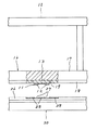
図1に示す回路検査治具は、上治具のヘッド板16を構成する保護板18付きベース17の保護板切り欠き部19に、プリント配線板26の凹形の回路パターン27に対向する導電接触部12を絶縁被膜28の厚み(回路パターン27の凹みの深さ)よりも大きく突出させた凹凸形状の導電ゴムからなる導電ヘッド11を接着したヘッドベース13を、導電接触部12が保護板切り欠き部19外に、すなわちヘッド板16の下方に絶縁被膜28の厚み以上に突出するように、ベース17の下面に対する接着を介して取り付けた構造からなっている。
【0010】
この回路検査治具では、プリント配線板26を上治具と下治具のヘッド板16、20間に挟んで保持することにより、上治具のヘッド板16の下方に突出する導電ヘッド11の導電接触部12を、プリント配線板26の回路パターン27の凹部に突入させて、回路パターン27に導電接触させることができる。
【0011】
この発明はこのほか、導電ヘッドを凹凸形状に成形した金属箔類で形成したり、上治具のヘッド板部に代えて、下治具のヘッド板部に上記の形態で導電ヘッドを取り付けるなど、種々の態様で実施することができるもので、図示の態様に限定されるものではない。
【0012】
【発明の効果】
以上説明したところから明らかなように、この発明に係る回路検査治具(導電ヘッドの導電接触構造)によれば、導電ヘッドを、プリント配線板挟持用のヘッド板に取り付けるとともに、導電ヘッドに絶縁被膜欠落部を通して回路パターンに接触可能な凸形の導電接触部を設けるので、ヘッド板によるプリント配線板の挟持力に対応する低圧力で、回路パターンに確実に接触させることができる。
【0013】
またこの回路検査治具によれば、エアシリンダやエア導管及びこれらの作動操作手段が不要なきわめてコンパクトな構造であるので、導電ヘッドの近傍部も含めて、コンタクトプローブ類を併設することができる。
【図面の簡単な説明】
【図1】この発明に係るプリント配線板の回路検査治具の実施態様の要部の一部を切り欠いた正面図である。
【図2】従来の回路検査治具の要部の一部を切り欠いた正面図である。
【符号の説明】
11 導電ヘッド
12 導電接触部
13 ヘッドベース
16 ヘッド板
17 ベース
18 保護板
19 保護板切り欠き部
20 ヘッド板
26 プリント配線板
27 回路パターン
28 絶縁被膜[0001]
[Technical field to which the invention belongs]
The present invention relates to a circuit inspection jig for a printed wiring board provided with a conductive head that is in conductive contact with a concave (concave surface) circuit pattern exposed at an insulating film missing portion of a printed wiring board, and in particular, a conductive head in the circuit inspection jig. The present invention relates to improvement of the conductive contact structure.
[0002]
[Prior art]
As shown in FIG. 2, a conductive head 21 in a conventional printed wiring board circuit inspection jig is attached to a
[0003]
[Problems to be solved by the invention]
However, a conventional circuit in which such a flat conductive head 21 is attached to the tip of the
[0004]
In view of the problems observed in the conventional circuit inspection jig with a conductive head as described above, the present invention ensures that the conductive head contacts the concave circuit pattern of the printed wiring board without using an air cylinder and with a small pressure. It is an object of the present invention to provide a printed circuit board inspection jig having a compact structure that can be provided with contact probes including the vicinity of the conductive head.
[0005]
In the circuit inspection jig according to the present invention, the conductive head is attached to the head board for sandwiching the printed wiring board of the upper jig or the lower jig, and the conductive head can be contacted with the circuit pattern of the printed wiring board through the insulating film. It has the structure which provided the convex-shaped electroconductive contact part which protrudes in the .
[0006]
In general, the conductive head can be formed of conductive rubber from the viewpoint of high form (shape) adaptability due to elastic deformation.
[0007]
In the circuit inspection jig according to the present invention, if the printed wiring board is sandwiched between the head plate of the upper jig and the lower jig , the convex conductive contact portion of the conductive head protruding outward is the printed wiring board. while the insulation film missing portion conductively contacts the concave circuit pattern through, if release the holding by the head plates, conductive contact is released to the circuit pattern by retraction of the conductive head.
[0008]
DETAILED DESCRIPTION OF THE INVENTION
Next, an embodiment of the circuit inspection jig according to the present invention will be described with reference to FIG.
[0009]
The circuit inspection jig shown in FIG. 1 has a conductive plate facing the
[0010]
In this circuit inspection jig, the printed
[0011]
In addition to this, the conductive head is formed of a metal foil formed into an uneven shape, or the conductive head is attached to the head plate portion of the lower jig instead of the head plate portion of the upper jig, etc. The present invention can be implemented in various modes, and is not limited to the illustrated modes.
[0012]
【The invention's effect】
As is apparent from the above description, according to the circuit inspection jig (conductive contact structure of the conductive head) according to the present invention, the conductive head is attached to the head plate for holding the printed wiring board and insulated from the conductive head. Since the convex conductive contact portion that can contact the circuit pattern through the missing film portion is provided , the circuit pattern can be reliably brought into contact with a low pressure corresponding to the holding force of the printed wiring board by the head plate.
[0013]
Further, according to this circuit inspection jig, since it has an extremely compact structure that does not require an air cylinder, an air conduit, and their operation operation means, contact probes including the vicinity of the conductive head can be additionally provided. .
[Brief description of the drawings]
FIG. 1 is a front view in which a part of an essential part of an embodiment of a circuit inspection jig for a printed wiring board according to the present invention is cut away.
FIG. 2 is a front view in which a part of a main part of a conventional circuit inspection jig is cut away.
[Explanation of symbols]
DESCRIPTION OF
Claims (1)
Priority Applications (1)
| Application Number | Priority Date | Filing Date | Title |
|---|---|---|---|
| JP18835196A JP3655397B2 (en) | 1996-06-28 | 1996-06-28 | Circuit inspection jig for printed wiring boards |
Applications Claiming Priority (1)
| Application Number | Priority Date | Filing Date | Title |
|---|---|---|---|
| JP18835196A JP3655397B2 (en) | 1996-06-28 | 1996-06-28 | Circuit inspection jig for printed wiring boards |
Publications (2)
| Publication Number | Publication Date |
|---|---|
| JPH1019935A JPH1019935A (en) | 1998-01-23 |
| JP3655397B2 true JP3655397B2 (en) | 2005-06-02 |
Family
ID=16222112
Family Applications (1)
| Application Number | Title | Priority Date | Filing Date |
|---|---|---|---|
| JP18835196A Expired - Fee Related JP3655397B2 (en) | 1996-06-28 | 1996-06-28 | Circuit inspection jig for printed wiring boards |
Country Status (1)
| Country | Link |
|---|---|
| JP (1) | JP3655397B2 (en) |
-
1996
- 1996-06-28 JP JP18835196A patent/JP3655397B2/en not_active Expired - Fee Related
Also Published As
| Publication number | Publication date |
|---|---|
| JPH1019935A (en) | 1998-01-23 |
Similar Documents
| Publication | Publication Date | Title |
|---|---|---|
| EP1005086A3 (en) | Metal foil having bumps, circuit substrate having the metal foil, and semiconductor device having the circuit substrate | |
| JP3279589B2 (en) | Printed wiring board | |
| JPH0275178A (en) | Cathode edge connector for solderless surface mounting | |
| US4197586A (en) | Electronic calculator assembly | |
| JP2017182880A (en) | Terminal block and electronic apparatus | |
| JP3655397B2 (en) | Circuit inspection jig for printed wiring boards | |
| JP2509855B2 (en) | Connection member for circuit board and connection structure using the connection member | |
| JPH09307208A (en) | Flexible printed circuit board connection end structure | |
| JP2870021B2 (en) | Circuit board for mounting components | |
| JP2002151806A (en) | Flexible wiring board | |
| JPS6011557Y2 (en) | Connection device for thermal recording head | |
| JPH11339903A (en) | Substrate mount connector | |
| JPH021917Y2 (en) | ||
| JPH10289641A (en) | Electromagnetic relay | |
| JP2002110273A (en) | FPC connector | |
| JPS5812474Y2 (en) | electrical equipment case | |
| JPS5846537Y2 (en) | connection device | |
| JPH0644124Y2 (en) | Microwave circuit connection structure | |
| JPH0783165B2 (en) | Circuit board | |
| JPS5939418Y2 (en) | circuit board equipment | |
| JPH08138485A (en) | Pressure-sensitive switch element | |
| JPS6214718Y2 (en) | ||
| JPH0217504Y2 (en) | ||
| JPS60239096A (en) | Connection structure of conductor pattern | |
| JP2001251087A (en) | Electromagnetic wave shield structure |
Legal Events
| Date | Code | Title | Description |
|---|---|---|---|
| A977 | Report on retrieval |
Free format text: JAPANESE INTERMEDIATE CODE: A971007 Effective date: 20041129 |
|
| A131 | Notification of reasons for refusal |
Free format text: JAPANESE INTERMEDIATE CODE: A131 Effective date: 20041216 |
|
| A521 | Request for written amendment filed |
Free format text: JAPANESE INTERMEDIATE CODE: A523 Effective date: 20050117 |
|
| TRDD | Decision of grant or rejection written | ||
| A01 | Written decision to grant a patent or to grant a registration (utility model) |
Free format text: JAPANESE INTERMEDIATE CODE: A01 Effective date: 20050207 |
|
| A61 | First payment of annual fees (during grant procedure) |
Free format text: JAPANESE INTERMEDIATE CODE: A61 Effective date: 20050303 |
|
| R150 | Certificate of patent or registration of utility model |
Free format text: JAPANESE INTERMEDIATE CODE: R150 |
|
| FPAY | Renewal fee payment (event date is renewal date of database) |
Free format text: PAYMENT UNTIL: 20090311 Year of fee payment: 4 |
|
| FPAY | Renewal fee payment (event date is renewal date of database) |
Free format text: PAYMENT UNTIL: 20090311 Year of fee payment: 4 |
|
| FPAY | Renewal fee payment (event date is renewal date of database) |
Free format text: PAYMENT UNTIL: 20100311 Year of fee payment: 5 |
|
| FPAY | Renewal fee payment (event date is renewal date of database) |
Free format text: PAYMENT UNTIL: 20110311 Year of fee payment: 6 |
|
| FPAY | Renewal fee payment (event date is renewal date of database) |
Free format text: PAYMENT UNTIL: 20110311 Year of fee payment: 6 |
|
| LAPS | Cancellation because of no payment of annual fees |