JP3649877B2 - Hybrid time slot and sub time slot operation in time division multiplexing systems - Google Patents
Hybrid time slot and sub time slot operation in time division multiplexing systems Download PDFInfo
- Publication number
- JP3649877B2 JP3649877B2 JP27633397A JP27633397A JP3649877B2 JP 3649877 B2 JP3649877 B2 JP 3649877B2 JP 27633397 A JP27633397 A JP 27633397A JP 27633397 A JP27633397 A JP 27633397A JP 3649877 B2 JP3649877 B2 JP 3649877B2
- Authority
- JP
- Japan
- Prior art keywords
- time slot
- sub
- port circuit
- port
- bus
- Prior art date
- Legal status (The legal status is an assumption and is not a legal conclusion. Google has not performed a legal analysis and makes no representation as to the accuracy of the status listed.)
- Expired - Fee Related
Links
- 238000012546 transfer Methods 0.000 claims description 32
- 239000000872 buffer Substances 0.000 description 23
- 238000004891 communication Methods 0.000 description 14
- 235000008429 bread Nutrition 0.000 description 12
- WIUGDTDEQHIWAS-UHFFFAOYSA-N sodium;[3-[[3-[(2-bromoacetyl)amino]phenoxy]-hydroxyphosphoryl]oxy-5-(5-methyl-2,4-dioxopyrimidin-1-yl)oxolan-2-yl]methyl [3-[(2-bromoacetyl)amino]phenyl] hydrogen phosphate Chemical compound [Na+].O=C1NC(=O)C(C)=CN1C1OC(COP(O)(=O)OC=2C=C(NC(=O)CBr)C=CC=2)C(OP(O)(=O)OC=2C=C(NC(=O)CBr)C=CC=2)C1 WIUGDTDEQHIWAS-UHFFFAOYSA-N 0.000 description 12
- 230000006870 function Effects 0.000 description 10
- 238000010586 diagram Methods 0.000 description 7
- DOIRQSBPFJWKBE-UHFFFAOYSA-N dibutyl phthalate Chemical compound CCCCOC(=O)C1=CC=CC=C1C(=O)OCCCC DOIRQSBPFJWKBE-UHFFFAOYSA-N 0.000 description 6
- 238000005516 engineering process Methods 0.000 description 5
- 238000000034 method Methods 0.000 description 5
- 238000012986 modification Methods 0.000 description 5
- 230000004048 modification Effects 0.000 description 5
- QYSGYZVSCZSLHT-UHFFFAOYSA-N octafluoropropane Chemical compound FC(F)(F)C(F)(F)C(F)(F)F QYSGYZVSCZSLHT-UHFFFAOYSA-N 0.000 description 4
- 238000013461 design Methods 0.000 description 2
- 238000012545 processing Methods 0.000 description 2
- 230000005540 biological transmission Effects 0.000 description 1
- 238000011161 development Methods 0.000 description 1
- 230000003467 diminishing effect Effects 0.000 description 1
- 230000009977 dual effect Effects 0.000 description 1
- 230000002452 interceptive effect Effects 0.000 description 1
- 230000007246 mechanism Effects 0.000 description 1
- 230000003252 repetitive effect Effects 0.000 description 1
- 230000004044 response Effects 0.000 description 1
- 230000001360 synchronised effect Effects 0.000 description 1
Images
Classifications
-
- H—ELECTRICITY
- H04—ELECTRIC COMMUNICATION TECHNIQUE
- H04Q—SELECTING
- H04Q11/00—Selecting arrangements for multiplex systems
- H04Q11/04—Selecting arrangements for multiplex systems for time-division multiplexing
Landscapes
- Engineering & Computer Science (AREA)
- Computer Networks & Wireless Communication (AREA)
- Time-Division Multiplex Systems (AREA)
- Use Of Switch Circuits For Exchanges And Methods Of Control Of Multiplex Exchanges (AREA)
Description
【0001】
【発明の属する技術分野】
本発明は、一般に時分割多重(TDM)システムに関し、特にTDM通信交換システムに関する。
【0002】
【従来の技術及び発明が解決しようとする課題】
時分割多重化は、一般に、最新の通信交換システムの交換機に使用されている。その一例は、ルーセント テクノロジーズ インクのDefinityR構内交換機(PBX)のTDMバスである。最新のアプリケーションやテクノロジーは、このような既存のTDMシステムのバス容量を急速に使い尽くしてしまう。例えば、マルチメディア通信は、ラインポートまたは中継線ポート当たり多数のタイムスロットを使用するが、最新のハードウェア テクノロジーは、ポートが各ポート回路パックを介して実行されるのを絶えず可能にする。したがって、TDMシステムのバス容量を増加させることが必要である。
【0003】
TDMバス容量を増加させる方法の1つは、バスをより早く、すなわちより高いクロック速度で、走らせることである。この方法は、TDMバスに接続してそれを使用する全ての回路パックの最新設計を必要とする。これは大規模な開発とコスト増加になる。したがって、この方法は、既存のシステムによる互換性が必要とされない新しいシステム設計においてのみ、使用に適している。
【0004】
TDMバス容量を増加させる第2の方法は、より高速のマルチフェーズ クロック分配を既存のTDMバスに追加することである。この方法は、既存の回路パックが従来の動作のために既存のクロックを使用するのを可能にすると共に、新しい回路パックが、多数のサブタイムスロット転送が1タイムスロットにおいて生じるサブタイムスロット動作のために新しい多相クロックを使用するのを可能にする。このような方法の一例は、米国特許第4,656,627号に開示されている。この方法は、新しいバス バックプレーン及びクロック発生回路を必要とし、既存システムのグレードアップを難しくかつ高価にさせる。したがって、技術があまりない者には、既存のシステムに容易に再適合すると共に、既存のポート回路パック及びバス バックプレーンの動作と干渉せずかつそれらの変更を要しない、TDMシステムのバス容量を増加させる方法である。
【0005】
【課題を解決するための手段】
本発明は、従来技術の欠点を解決してその要求を満足させることに向けられている。本発明によれば、ポート回路は、従来のタイムスロット動作を遂行するばかりでなく、外部の支援なしにサブタイムスロット動作を遂行するように設計される。例えば、周波数乗算されたフェーズロックループ(PLL)等のクロック周波数乗算器と、PLL駆動式有限状態装置等の乗算器駆動式サブタイムスロット動作回路が、新しいポート回路パックに組み込まれる。クロック周波数乗算機及びサブタイムスロット動作回路は、1タイムスロットにおける多数のTDMバス転送を遂行するのに必要な追加の制御信号の全てを発生する。サブタイムスロット動作は、過タイムスロットを基礎として機能付与され、それにより、サブタイムスロット動作は同一TDMバス上の標準動作と共存することができる。また、それは、新しいポート回路パックが従来のポート回路パックと共に標準的なタイムスロット動作に従事するのを可能にする。新しいポート回路パックは、既存のポート回路パック及びTDMバス バックプレーンと干渉することなくまたはそれらのいかなる変更も必要とすることなく動作する。したがって、既存のTDMシステムへの再適合とそのアップグレードは、簡単であり、遂行が比較的安価である。
【0006】
一般に本発明の一態様によれば、交換システムは、各々が予め決められた持続時間を有する複数のタイムスロットを定義するTDM交換機と、前記交換機に接続され、各々がいずれかの1タイムスロットの間前記交換機を介して1つだけの情報転送を遂行する複数の第1の(従来の)ポート回路と、前記交換機に接続され、各々が、(a)いずれかの1タイムスロットの間前記交換機を介して1つだけの情報転送か、または(b)1タイムスロットの間前記交換機を介して複数回の情報転送を遂行するように、いずれかの1サブタイムスロットの間前記交換構造を介して1つの情報転送かのどちらかを選択的に遂行するために、各々の前記タイムスロットの間複数のサブタイムスロットを定義する複数の第2のポート回路とからなる。したがって、サブタイムスロット機能付与されたポート回路は、好適に、TDM交換システムにおけるハイブリッド タイムスロット及びサブタイムスロット動作が可能である。サブタイムスロット機能付与されたポート回路は、第1のポート回路と共に1タイムスロットの間交換機を介して1つの転送を遂行し、それにより、第1のポート回路と互換性があり、また、他のサブタイムスロット機能付与されたポート回路と共に1サブタイムスロットの間交換機を介して1つの転送を遂行し、それにより、TDM交換機の転送処理量を増加させる。
【0007】
好適には、交換システムは、全ポート回路へのタイムスロットを定義する第1のクロック信号を運び、サブタイムスロット機能付与されたポート回路は、受信した第1のクロック信号を乗算して、それからサブタイムスロットを定義する第2のクロック信号を発生する。したがって、サブタイムスロット機能付与されたポート回路は、交換システムが従来のポート回路に従来提供している支援以外の交換システムからのどんな支援もなしに、サブタイムスロット動作を遂行する。また、好適には、サブタイムスロット機能付与されたポート回路は、あるタイムスロットの複数のサブタイムスロットをそのタイムスロットと同期させ、それにより、タイムスロットの時間境界がサブタイムスロット転送により邪魔されないことを確実にする装置を含む。さらに、好適には、サブタイムスロット機能付与されたポート回路は、有限状態装置を使用して、サブタイムスロット同作用の制御信号を発生させる。有限状態装置は、制御メカニズムのリソース効率的な比較的安価な実行となる。好適には、有限状態装置は、その状態の一部として同期化装置を実行し、それにより、この機能を実行するための別個の回路の必要性をなくしている。
【0008】
本発明のこれら及び他の利点及び特徴は、図面と共に行われる本発明の実施例の以下の説明からより明らかになるだろう。
【0009】
【発明の実施の形態】
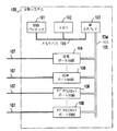
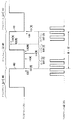
図1は、本発明の一実施例108を組み込んだ例示的なTDM通信交換システム100を示す。交換システム100は、例えば、ルーセント テクノロジーズインクのDefinity(登録商標)PBXである。交換システム100は制御プロセッサ101、メモリ102及び網インターフェース103からなり、これらはメモリバスで相互接続されている。網インターフェース103は、プロセッサ101に時分割多重化(TDM)バス105へのアクセスを提供する。TDMバス105は交換システム100の通信交換媒体−−交換機−−として役立つ。Definity PBXでは、TDMバス105は、並列に動作すると共に、各々がTDMバス105の半分の容量(タイムスロット)を有する2つのTDMバス(A+B)からなる。制御プロセッサ101は、交換システム100の動作を制御すると共に通信機能を実行する。通信機能には、呼処理や、TDMバス105に接続された個々のポート回路106及び108で使用されるTDMバス105のタイムスロットの割り当てが含まれる。その機能を実行するために、プロセッサ101は、TDMバス105を介して、ポート回路106及び108と、それに接続された通信線及び中継線107と通信する。ポート回路106及び108は、従来のポート回路106及びサブタイムスロット ポート回路108を含む。サブタイムスロット ポート回路108は本発明の原理に従って構成される。
【0010】
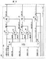
Definity PBXの従来のポート回路106は、サニティ アンド コントロール インターフェース(SAKI)と、TDMバス用スイッチ カンファレンサー及び集中ハイウェイ(SCOTCH)と、一対の集中ハイウェイとによってTDMバス105に接続され、インターフェースされている。SAKIは、TDMバス105を介して制御プロセッサ101と制御メッセージをやり取りする。SAKIは、標準システム100制御メッセージをTDMバス105の通信プロトコルに変換したり、TDMバス105の通信プロトコルから標準システム100制御メッセージを変換したりする。SAKIは、TDMバス105からのメッセージの受信に基づいて中断を生じ、中断の受信に応答してTDMバス105への出力用のメッセージを受け入れる。SCOTCHは、集中ハイウェイとTDMバス105の間で多数の音声及び/またはデータ通信チャンネルを接続する集中/集中解除装置である。SCOTCHは、第1の集中ハイウェイを介して集中のための多数のチャンネルを受信し、集中解除されたチャンネルを第2の集中ハイウェイ上に出力する。各集中ハイウェイは、各々の反復フレームにおいて64チャンネルまで適応する従来の受動シリアルTDMバスである。
【0011】
サブタイムスロット ポート回路108では、従来のポート回路106のSCOTCHと集中ハイウェイは図2に示される回路で置換される。ポート回路108は、TDMAバッファ200及びTDMBバッファ201でTDMバスのデータ線209に接続される。バッファ200及び201は、TDMバス105のタイムスロットへ/からデータ及び制御情報のバイトを送信/受信する。Definity PBXでは、TDMAバッファ200は、TDMバス105を構成する2つのバスのうちの一方のデータ線に接続し、TDMBバッファ201は、TDMバス105を構成する2つのバスのうちの他方のデータ線に接続する。回路108の内部で、バッファ200及び201は、それぞれ一対のバスTDMA210及びTDMB211に接続し、これらを介して、TDMバス105から受信したバイトを送信すると共に、これらから、TDMバス105への送信のためのバイトを受信する。
【0012】
バス210及び211は、それぞれ、TDMA読み取り(AR)バッファ205及びTDMA書き込み(AW)ラッチ206と、TDMB読み取り(BR)バッファ207及びTDMB書き込み(BW)ラッチ208とによってMUX A+Bバス212にインターフェースされる。ARバッファ205は、TDMAバス210からの情報がMUX A+Bバス212で読み取られるのを可能にし、AWラッチ206は、MUX A+Bバス212からの情報がTDMAバス210上に書き込まれるのを可能にする。同様に、BRバッファ207は、TDMAバス211からの情報がMUX A+Bバス212で読み取られるのを可能にし、BWラッチ208は、MUX A+Bバス212からの情報がTDMAバス211上に書き込まれるのを可能にする。同時に、構成要素205〜208は、バス212とバス210〜211間のマルチプレクサ/デマルチプレクサとして機能する。MUX A+Bバス212は、ポート回路108の他の(従来の)回路とデータ及び制御情報をやり取りする。
【0013】
また、TDMバス105のTDM CLK線213及びFRAME CLK線214も回路108に接続される。TDM CLK線213は、TDMバス105上の全タイムスロットに時間が合ったクロック信号を交換システム100中に分配する。これらは例えば2.048MHz信号である。FRAME CLK線214は、TDMバス105上のタイムスロットのフレームに時間が合ったクロック信号を分配する。これらは例えば8KHz信号である。TDM CLK線213は従来の周波数多重化PLL202に接続される。周波数多重化PLL202は、TDMタイムスロット クロック信号を32倍だけ周波数乗算し、乗算した信号をTDMタイムスロット クロック信号と同期させる。PLL202は、乗算したクロック信号をTDM CLKx32線215に出力する。
【0014】
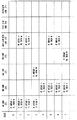
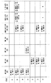
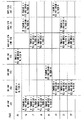
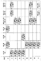
クロック信号線213及び215は、ポート回路108の他の回路ばかりでなく有限状態装置203にも接続される。状態装置203は、線213及び215より受信したクロック信号を使用して、ポート回路108の動作を制御するためのサブタイムスロット制御信号を発生する回路である。クロック信号のほかにも、状態装置203は、AREAD信号線218及びBREAD信号線219も入力として持っている。状態装置203は、AREAD信号線218及びBREAD信号線219より、それぞれ、TDMAバス210及びTDMBバス211を読み取るかまたは書き込むべきかどうかに関するポート回路108の他の回路からの命令を受け取る。状態装置203は、さらに、TDM SUBA信号線220及びTDM SUBB信号線221も入力として持っている。状態装置203は、TDM SUBA信号線220及びTDM SUBB信号線221より、TDMバス105のそれぞれ一部A及びBにおいて従来のタイムスロット動作またはサブタイムスロット動作に従事させるべきかどうかに関するポート回路108の他の回路からの命令を受け取る。状態装置203は、例えばプログラマブル ロジックアレイ(PLA)で実行される。状態装置203は、図3に示される32状態とそれらの対応する制御信号を実行する。
【0015】
図4に示されるように、TDMバス105上の各々の従来のタイムスロット400〜402は、TDM CLK線213上のクロック信号の1サイクル全体で定義され、そのクロック信号の立ち下がりエッジで終わる。状態装置203は、デジタルPLL204よりのタイムスロット クロック信号の立ち下がりエッジ403に同期される。デジタルPLL204は、好適には状態装置203の最後の2状態30及び31として実行される。状態装置203は図3の状態30でスタートし、ここで、タイムスロット クロック信号の立ち下がりエッジ403の間TDM CLK信号線213を監視する。図4の時間t(31)で起こるタイムスロット クロック信号立ち下がりエッジ403はタイムスロットの終わりを合図し、状態装置203は図3の状態31に進み、ここで、図2のBUFA R/W及びBUFB R/W制御線222及び223上に“読み取り”信号を発し、TDMAバッファ200及びTDMBバッファ201にTDMバス105から1バイトの情報(データまたは制御)を読み取らせる。(これは、従来のポート回路106がTDMバス105の1タイムスロットを読み取る時間である。)
【0016】
TDM CLKx32線215上の乗算された信号の次の瞬間は次のタイムスロット400〜402の始まりを合図し、状態装置203は図3の状態0に進む。状態0では、状態装置203へのAREAD入力信号線218が、TDMAバス210が読み取られるべきであることを示す“読み取り”状態にある場合は、状態装置203は、AR制御線222上に“読み取り”信号を発し、ARバッファ205にMUX A+Bバス212上にその内容を出力させる。次いで、状態装置203は、次の3状態の間AR制御線222の“読み取り”信号を維持し、MUX A+Bバス212に取り付けられた装置にバス212を読み取るのに十分な時間を与える。乗算されたクロック信号の次の瞬間に、状態装置203は状態1に進む。状態1では、AREAD線218が“書き込み”状態にある場合は、状態装置203は、MUX A+B R/W制御線226に“書き込み”信号を発し、MUX A+Bバス212に接続されたポート回路108の装置(例えばDSP、図示しない)にバス212を書き込ませる。TDM CLKx32線215上の乗算された制御信号の次の瞬間に、状態装置203は状態2に進む。状態2では、AREAD線218が“読み取り”状態にある場合は、状態装置203は、MUX A+B R/W線226上に“読み取り”信号を発し、MUXA+Bバス212に接続されたポート回路108の装置にバス212を読み取らせる。乗算されたクロック信号の次の瞬間に、状態装置203は状態3に進む。状態3では、AREAD線218が“書き込み”状態にある場合は、状態装置203は、AW線223上に“書き込み”信号を発し、AWラッチ206にMUX A+Bバス212からのデータをラッチさせる。乗算されたクロック信号の次の瞬間に、状態装置203は状態4に進む。状態4では、状態装置203へのBREAD入力信号線219が“読み取り”状態にある場合は、状態装置203は、BR制御線224上に“読み取り”信号を発し、BRバッファ207にMUX A+Bバス212上にその内容を出力させる。次いで、状態装置203は、次の3状態の間BR制御線224の“読み取り”信号を維持する。乗算されたクロック信号の次の瞬間に、状態装置203は状態5に進む。
【0017】
状態5では、BREAD線219が“書き込み”状態にある場合は、状態装置203は、MUX A+B R/W制御線226に“書き込み”信号を発し、MUX A+Bバス212に接続されたポート回路108の装置にバス212を読み取らせる。乗算された制御信号の次の瞬間に、状態装置203は状態6に進む。状態6では、BREAD線218が“読み取り”状態にある場合は、状態装置203は、MUX A+B R/W線226上に“読み取り”信号を発し、MUX A+Bバス212に接続されたポート回路108の装置にバス212を読み取らせる。乗算されたクロック信号の次の瞬間に、状態装置203は状態7に進む。状態7では、BREAD線218が“書き込み”状態にある場合は、状態装置203は、BW制御線225上に“書き込み”信号を発し、BWラッチ208にMUX A+Bバス212からのデータをラッチさせる。乗算されたクロック信号の次の瞬間に、状態装置203は状態8に進む。
【0018】
状態8では、AREAD線218が“読み取り”状態にある場合は、状態装置203は、AR線222上に“読み取り”信号を発し、ARバッファ205にMUX A+Bバス212上にその内容を出力させる。次いで、状態装置203は、次の3状態の間AR制御線223の“読み取り”信号を維持する。また状態8で、AREAD線218またはBREAD線219が“書き込み”状態にある場合は、状態装置203は、BUFA R/W線216及びBUFB R/W線217に“書き込み”信号を発し、バッファ200及び201にそれらの内容をTDMバス105上に書き込ませる。(これは、ほぼ、従来のポート回路106がTDMバス105の1タイムスロットを書き込む時間である。)乗算された制御信号の次の瞬間に、状態装置203は状態9〜14に進み、ここでは、それぞれ状態1〜6の作業を繰り返す。さらに状態14では、状態装置203は同様にBUFA R/W線216及びBUFB R/W線217に“読み取り”信号を発し、TDMA及びTDMBバッファ200及び201にTDMバス105からのデータを読み取らせる。図4に示されるように、TDMバス105の1タイムスロットの第1のサブタイムスロットはこの時点で終わり、第2のサブタイムスロットが始まる。
【0019】
図3に示される状態15〜30の動作は、TDM SUBA及びTDM SUBB入力信号線220及び221が、ポート回路108がサブタイムスロット動作に従事すべきであることを示している場合のみ実行され、さもなければ、これらの状態は状態装置203により“不動作”になる。乗算されたクロック信号の次の瞬間に、状態装置203は状態15に進む。状態15では、状態装置203へのTDM SUBB入力信号線221が、サブタイムスロット動作がTDMバス105の一部Bで遂行されるべきであることを示す“イエス”状態にあり、かつ、BREAD線219が、TDMBバス211が書き込まれるべきであることを示す“書き込み”状態にある場合は、状態装置203はBW線225に“書き込み”信号を発し、BWラッチ208にMUX A+Bバス212からのデータをラッチさせる。乗算されたクロック信号の次の瞬間に、状態装置203は状態16に進む。
【0020】
状態16では、状態装置203へのTDM SUBA入力信号線220が、サブタイムスロット動作がTDMバス105の一部Aで遂行されるべきであることを示す“イエス”状態にあり、かつ、AREAD線219が、TDMBバス211が読み取られるべきであることを示す“読み取り”状態にある場合は、状態装置203はAR線222に“読み取り”信号を発し、ARバッファ205にその内容をMUX A+Bバス212に出力させる。次いで、状態装置203は次の3状態の間AR線222の“読み取り”信号を維持する。また状態16において、TDM SUBA線220またはTDM SUBB線221−−あるいはその両方−−が“イエス”状態にあり、かつ、対応するAREAD線218またはBREAD線219−−あるいはその両方−−が“書き込み”状態にある場合は、状態装置203は、BUFA R/W線216またはBUFB R/W線217−−あるいはその両方−−にそれぞれ“書き込み”を発し、それぞれTDMAバッファ200またはTDMBバッファ201−−あるいはその両方−−にそれらの内容をTDMバス105に書き込ませる。乗算されたクロック信号の次の3回の瞬間に、状態装置203は状態17〜19に進み、ここで、TDM SUBA線220が“イエス”状態にある場合に、それぞれ状態1〜3の作業を繰り返す。乗算されたクロック信号の次の2回の瞬間に、状態装置203は状態20〜21に進み、ここで、TDM SUBBが“イエス”状態にある場合に、それぞれ状態4〜5の作業を繰り返す。
【0021】
乗算されたクロック信号の次の瞬間に、状態装置203は状態22に進む。状態22では、TDM SUBB線221が“イエス”状態にあり、BREAD線219が“読み取り”状態にある場合は、状態装置203は、MUX A+B R/W線226に“読み取り”信号を発し、MUX A+Bバス212に接続されたポート回路108の装置にバス212を読み取らせる。また状態22では、TDM SUBA線220またはTDM SUBB線221−−あるいはその両方−−が“イエス”状態にあり、同様に、対応するAREAD線218またはBREAD線219−−あるいはその両方−−が“読み取り”状態にある場合は、状態装置203は、BUFA R/W線216またはBUFB R/W線217−−あるいはその両方−−にそれぞれ“読み取り”信号を発し、それぞれのTDMAバッファ200またはTDMBバッファ201−−あるいはその両方−−にTDMバス105からのデータを読み取らせる。この時点で、図3に示されるように、TDMバス105の1タイムスロットの第2のサブタイムスロットは終わりになり、次いで、第3のサブタイムスロットが始まる。
【0022】
乗算されたクロック信号の次の7回の瞬間では、状態装置203は状態23〜29に進み、ここでは、それぞれ状態15〜21の作業を繰り返す。乗算されたクロック信号の次の瞬間に、状態装置203は状態30に進む。状態30では、TDM SUBB線221が“イエス”状態にあり、BREAD線219が“読み取り”状態にある場合は、状態装置203は、MUX A+B R/W線226に“読み取り”信号を発し、MUX A+Bバス212に接続されたポート回路108の装置にバス212を読み取らせる。状態装置203は、タイムスロット クロック信号の立ち下がりエッジ403が生じたことを示すローレベルを検出するまで、状態30に留まる。その時点−−通常、乗算されたクロック信号の次の瞬間に実質的に起こる−−で、状態装置203は状態31に進む。状態31では、状態措置203は、BUFA R/W線216及びBUFB R/W線217に“読み取り”コマンドを発し、バッファ200及び201にTDMバス105からのデータを読み取らせて記憶させる。図3に示されるように、この時点で、TDMバス105の1タイムスロットと第3のサブタイムスロットは共に終わりになり、次いで、新しいTDMバス105の1タイムスロットとその第1のサブタイムスロットが始まる。
【0023】
図示され上記に説明されたように、ポート回路108は、TDMバスの1タイムスロット中にTDMバス105を介して従来の1つの転送か、またはTDMバス105の1タイムスロットの時間の間に、3回の転送すなわち3回のサブタイムスロット動作のどちらかを実行するように選択的に機能付与される。したがって、ポート回路108は、前の転送により従来のポート回路106との通信かまたは後の転送により他のサブタイムスロット ポート回路108との通信のどちらかに従事することができる。後の転送は、TDMバス105の標準転送容量の3倍になる。その結果、従来及びサブタイムスロット ポート回路106及び108は、同一交換システム100において“調子を合わせる”ことができ、既存の交換システムへの再適合が可能になると共に実行も容易になる。さらに、従来の交換システムを修正する必要もない。
【0024】
もちろん、上記に説明された実施例の種々の変更や修正は当業者に明らかだろう。例えば、TDMバス105は二重バスである必要はなく単一バスでも良く、またはかけがえとして、バス212は多重化する必要がない。また、小分割されたタイムスロットにおいて複数の“話者”及び/または“聴取者”がいても良く、例えば、異なる装置が1タイムスロットの異なるサブタイムスロットにおいて送信及び/または受信することができる。このような変更や修正は、本発明の精神及び範囲を逸脱することなくかつ付随の利点をなくすことなく実行することができる。したがって、このような変更や修正は付随の請求の範囲で保護されるべきものである。
【図面の簡単な説明】
【図1】TDM通信交換システムの一例のブロック図である。
【図2】本発明に従って構成された図1のシステムのサブタイムスロット ポート回路の一部の一実施例のブロック図である。
【図3A】図2のポート回路の有限状態装置の状態図である。
【図3B】図2のポート回路の有限状態装置の状態図である。
【図3C】図2のポート回路の有限状態装置の状態図である。
【図3D】図2のポート回路の有限状態装置の状態図である。
【図4】図2のポート回路の動作のタイミング図である。[0001]
BACKGROUND OF THE INVENTION
The present invention relates generally to time division multiplexing (TDM) systems, and more particularly to TDM communication switching systems.
[0002]
[Prior art and problems to be solved by the invention]
Time division multiplexing is generally used in the switches of modern communication switching systems. One example is the TDM bus of Lucent Technologies, Inc.'s Definit® Private Branch Exchange (PBX). Modern applications and technologies quickly exhaust the bus capacity of such existing TDM systems. For example, multimedia communication uses a large number of time slots per line port or trunk port, but modern hardware technology constantly allows ports to be implemented through each port circuit pack. Therefore, it is necessary to increase the bus capacity of the TDM system.
[0003]
One way to increase the TDM bus capacity is to run the bus faster, i.e. at a higher clock speed. This method requires an updated design of all circuit packs that connect to and use the TDM bus. This will result in massive development and increased costs. Therefore, this method is only suitable for use in new system designs that do not require compatibility with existing systems.
[0004]
A second way to increase TDM bus capacity is to add a faster multi-phase clock distribution to the existing TDM bus. This method allows existing circuit packs to use existing clocks for conventional operation, and new circuit packs allow for sub-time slot operations where multiple sub-time slot transfers occur in one time slot. In order to be able to use a new multiphase clock. An example of such a method is disclosed in US Pat. No. 4,656,627. This method requires a new bus backplane and clock generation circuit and makes upgrading existing systems difficult and expensive. Therefore, for those with less technology, the bus capacity of the TDM system can be easily re-adapted to existing systems and does not interfere with the operation of existing port circuit packs and bus backplanes and requires no modification. It is a way to increase.
[0005]
[Means for Solving the Problems]
The present invention is directed to solving the shortcomings of the prior art and satisfying its needs. In accordance with the present invention, the port circuit is designed not only to perform a conventional time slot operation, but also to perform a sub time slot operation without external assistance. For example, a frequency-multiplied clock frequency multiplier, such as a phase-locked loop (PLL), and a multiplier-driven sub-time slot operation circuit, such as a PLL-driven finite state machine, are incorporated into the new port circuit pack. The clock frequency multiplier and sub time slot operation circuit generates all of the additional control signals necessary to perform multiple TDM bus transfers in one time slot. The sub time slot operation is functionalized on the basis of the over time slot, so that the sub time slot operation can coexist with the standard operation on the same TDM bus. It also allows new port circuit packs to engage in standard time slot operations with conventional port circuit packs. The new port circuit pack operates without interfering with or requiring any modification of existing port circuit packs and TDM bus backplanes. Thus, re-adaptation to an existing TDM system and its upgrade is simple and relatively inexpensive to perform.
[0006]
In general, according to one aspect of the present invention, a switching system includes a TDM switch that defines a plurality of time slots each having a predetermined duration, and is connected to the switch, each of which is one of the time slots. A plurality of first (conventional) port circuits that perform only one transfer of information through the switch, and are connected to the switch, each of which is (a) the switch for any one time slot Or only one information transfer via the exchange, or (b) via the exchange structure during any one sub-time slot, so as to perform multiple information transfers via the exchange during one time slot. A plurality of second port circuits defining a plurality of sub-time slots between each of the time slots in order to selectively perform one information transfer. Therefore, the port circuit provided with the sub time slot function is preferably capable of hybrid time slot and sub time slot operations in the TDM switching system. The port circuit provided with the sub time slot function performs one transfer through the exchange for one time slot together with the first port circuit, thereby being compatible with the first port circuit and the other. With the port circuit provided with the sub time slot function, one transfer is performed through the switch for one sub time slot, thereby increasing the transfer processing amount of the TDM switch.
[0007]
Preferably, the switching system carries a first clock signal defining a time slot to all port circuits, and the port circuit with sub-timeslot functionality is then multiplied by the received first clock signal and then A second clock signal defining a sub time slot is generated. Thus, a port circuit with sub-timeslot functionality will perform sub-timeslot operations without any assistance from the switching system other than the assistance that the switching system conventionally provides for conventional port circuits. Also preferably, the port circuit provided with the sub time slot function synchronizes a plurality of sub time slots of a certain time slot with the time slot so that the time boundary of the time slot is not disturbed by the sub time slot transfer. Including devices to ensure that. Furthermore, preferably, the port circuit provided with the sub time slot function uses a finite state machine to generate a control signal for the operation of the sub time slot. A finite state machine results in a resource efficient and inexpensive implementation of the control mechanism. Preferably, the finite state machine implements a synchronizer as part of its state, thereby eliminating the need for a separate circuit to perform this function.
[0008]
These and other advantages and features of the invention will become more apparent from the following description of embodiments of the invention taken together with the drawings.
[0009]
DETAILED DESCRIPTION OF THE INVENTION
FIG. 1 illustrates an exemplary TDM communications switching system 100 that incorporates one
[0010]
The
[0011]
In the sub time
[0012]
[0013]
In addition, the
[0014]
[0015]
As shown in FIG. 4, each conventional time slot 400-402 on the
[0016]
The next instant of the multiplied signal on the
[0017]
In state 5, if the
[0018]
In
[0019]
The operations of states 15-30 shown in FIG. 3 are performed only if the TDM SUBA and TDM SUBB
[0020]
In
[0021]
At the next moment of the multiplied clock signal,
[0022]
At the next seven moments of the multiplied clock signal,
[0023]
As shown and described above, the
[0024]
Of course, various changes and modifications to the embodiments described above will be apparent to those skilled in the art. For example, the
[Brief description of the drawings]
FIG. 1 is a block diagram of an example of a TDM communication switching system.
2 is a block diagram of one embodiment of a portion of the sub-timeslot port circuit of the system of FIG. 1 configured in accordance with the present invention.
3A is a state diagram of the finite state device of the port circuit of FIG. 2. FIG.
3B is a state diagram of the finite state device of the port circuit of FIG.
3C is a state diagram of the finite state device of the port circuit of FIG. 2;
3D is a state diagram of the finite state device of the port circuit of FIG.
4 is a timing diagram of the operation of the port circuit of FIG. 2;
Claims (10)
各タイムスロットの間に複数のサブタイムスロットを定義する装置と、
前記サブタイムスロット定義装置に接続され、(a)第1のポート回路を使用した、いずれかのタイムスロットの間に前記交換機を介する1つだけの情報転送と、(b)別の第2のポート回路を使用して1タイムスロットの間に前記交換機を介して複数の情報転送を遂行するために、いずれかの1サブタイムスロットの間に前記交換機を介する1つの情報転送とのうちのいずれか一方の情報転送を、または両方を選択的に遂行する装置と、からなるポート回路。A time division multiplex switch, each defining a plurality of time slots having a predetermined duration, and connected to the switch, each transferring only one information through the switch during any time slot. A port circuit for a switching system with a plurality of first port circuits only for performing,
A device for defining a plurality of sub-time slots during each time slot,
Said sub-time-slot is connected to a defined system, (a) using a first port circuit, and only the information transfer one that via the switch during either time slot, the second by (b) to perform a plurality of information transfer through the switch during the port circuits one time slot using, among the one information transfer via the switch during either one sub-time slot And a device for selectively performing either one of the information transfer or both .
前記交換機に接続され、各々がいずれかのタイムスロットの間に交換機を介して1つだけの情報転送を遂行するためだけの複数の第1のポート回路と、
前記交換機に接続される複数の第2のポート回路とからなり、各々の複数の第2のポート回路は前記の各タイムスロットの間に複数のサブタイムスロットを定義し、(a)第1のポート回路を使用した、いずれかのタイムスロットの間に前記交換機を介する1つだけの情報転送と、(b)別の第2のポート回路を使用して1タイムスロットの間に前記交換機を介して複数の情報転送を遂行するために、いずれかの1サブタイムスロットの間に前記交換機を介する1つの情報転送とのうちのいずれか一方の情報転送を、または両方を選択的に遂行する交換システム。A time division multiplex switch defining a plurality of time slots, each having a predetermined duration;
A plurality of first port circuits connected to the switch, each for performing only one information transfer through the switch during any time slot;
And a plurality of second port circuits that will be connected to the exchange, each plurality of second port circuits defining a plurality of sub-time slots during said each time slot, (a) a first with port circuit, and only the information transfer one that via the switch during either time slot, the exchange between one time slot using a second port circuit alternative (b) In order to perform a plurality of information transfers via one or more sub-slots, one or both of the information transfers via the exchange are selectively performed during one sub-time slot. Exchange system.
各々の第2のポート回路は、前記信号リンクに接続され、受信した前記第1のクロック信号を乗算して、前記第1のクロック信号からサブタイムスロットを定義する第2のクロック信号を発生する装置を含む交換システム。The switching system of claim 7, wherein the switch includes a signal link that carries a first clock signal defining a time slot to the port circuit;
Each second port circuit is connected to the signal link and multiplies the received first clock signal to generate a second clock signal defining a sub time slot from the first clock signal. Exchange system including equipment.
Applications Claiming Priority (2)
| Application Number | Priority Date | Filing Date | Title |
|---|---|---|---|
| US08/728,814 US5862131A (en) | 1996-10-10 | 1996-10-10 | Hybrid time-slot and sub-time-slot operation in a time-division multiplexed system |
| US08/728814 | 1996-10-10 |
Publications (2)
| Publication Number | Publication Date |
|---|---|
| JPH10136477A JPH10136477A (en) | 1998-05-22 |
| JP3649877B2 true JP3649877B2 (en) | 2005-05-18 |
Family
ID=24928372
Family Applications (1)
| Application Number | Title | Priority Date | Filing Date |
|---|---|---|---|
| JP27633397A Expired - Fee Related JP3649877B2 (en) | 1996-10-10 | 1997-10-09 | Hybrid time slot and sub time slot operation in time division multiplexing systems |
Country Status (5)
| Country | Link |
|---|---|
| US (1) | US5862131A (en) |
| EP (1) | EP0836358B1 (en) |
| JP (1) | JP3649877B2 (en) |
| CA (1) | CA2210841C (en) |
| DE (1) | DE69734864T2 (en) |
Families Citing this family (9)
| Publication number | Priority date | Publication date | Assignee | Title |
|---|---|---|---|---|
| JPH0887462A (en) | 1994-09-20 | 1996-04-02 | Fujitsu Ltd | State machine and communication control method |
| US20040213188A1 (en) * | 2001-01-19 | 2004-10-28 | Raze Technologies, Inc. | Backplane architecture for use in wireless and wireline access systems |
| US6738582B1 (en) * | 2002-03-26 | 2004-05-18 | Martisse Networks | Synchronization system for all optical slotted ring dynamic networks |
| US20050147411A1 (en) * | 2002-03-28 | 2005-07-07 | Matisse Networks | Optical reservation-based network switch fabrics |
| US20030227913A1 (en) * | 2002-06-05 | 2003-12-11 | Litchfield Communications, Inc. | Adaptive timing recovery of synchronous transport signals |
| US20040047367A1 (en) * | 2002-09-05 | 2004-03-11 | Litchfield Communications, Inc. | Method and system for optimizing the size of a variable buffer |
| AU2002364497A1 (en) * | 2002-12-27 | 2004-07-22 | Telefonaktiebolaget Lm Ericsson (Publ) | Method for reducing the bus load in a synchronous data bus system |
| US7912075B1 (en) * | 2006-05-26 | 2011-03-22 | Avaya Inc. | Mechanisms and algorithms for arbitrating between and synchronizing state of duplicated media processing components |
| US9081653B2 (en) | 2011-11-16 | 2015-07-14 | Flextronics Ap, Llc | Duplicated processing in vehicles |
Family Cites Families (13)
| Publication number | Priority date | Publication date | Assignee | Title |
|---|---|---|---|---|
| US4187399A (en) * | 1978-06-05 | 1980-02-05 | Bell Telephone Laboratories, Incorporated | Call state processor for a time division switching system |
| GB2128446B (en) * | 1982-10-02 | 1985-09-04 | Standard Telephones Cables Ltd | Telecommunication exchange |
| US4628446A (en) * | 1982-12-06 | 1986-12-09 | At&T Bell Laboratories | Multichannel interface |
| NL189591C (en) * | 1984-02-24 | 1993-05-17 | Nederland Ptt | DIGITAL SWITCHING NETWORK FOR THE FORWARDING OF TIME MULTIPLEX CHANNELS THAT MAY VARY BY CHANNEL OF CHANNEL SPEED. |
| US4656627A (en) * | 1984-11-21 | 1987-04-07 | At&T Company | Multiphase packet switching system |
| US4658152A (en) * | 1985-12-04 | 1987-04-14 | Bell Communications Research, Inc. | Adaptive rate multiplexer-demultiplexer |
| NL8600614A (en) * | 1986-03-10 | 1987-10-01 | At & T & Philips Telecomm | WIDE / NARROW BAND WIRING NETWORK OF TIME-SPACE-TIME TYPE AND TIME, SPACE SWITCHING STAGE FOR WIDE / NARROW CHANNELS. |
| US4791629A (en) * | 1986-06-02 | 1988-12-13 | Ibm Corporation | Communications switching system |
| US4965884A (en) * | 1989-11-22 | 1990-10-23 | Northern Telecom Limited | Data alignment method and apparatus |
| CA2068048A1 (en) * | 1991-05-06 | 1992-11-07 | Douglas D. Cheung | Fault tolerant processing section with dynamically reconfigurable voting |
| GB2286099B (en) * | 1991-05-31 | 1995-09-27 | Mitel Corp | Modular communication system with allocatable bandwidth |
| US5311576A (en) * | 1992-01-27 | 1994-05-10 | At&T Bell Laboratories | Adjunct processor embedded in a switching system |
| US5594727A (en) * | 1994-09-19 | 1997-01-14 | Summa Four, Inc. | Telephone switch providing dynamic allocation of time division multiplex resources |
-
1996
- 1996-10-10 US US08/728,814 patent/US5862131A/en not_active Expired - Lifetime
-
1997
- 1997-07-17 CA CA002210841A patent/CA2210841C/en not_active Expired - Fee Related
- 1997-09-30 DE DE69734864T patent/DE69734864T2/en not_active Expired - Fee Related
- 1997-09-30 EP EP97307694A patent/EP0836358B1/en not_active Expired - Lifetime
- 1997-10-09 JP JP27633397A patent/JP3649877B2/en not_active Expired - Fee Related
Also Published As
| Publication number | Publication date |
|---|---|
| US5862131A (en) | 1999-01-19 |
| CA2210841A1 (en) | 1999-01-17 |
| EP0836358A2 (en) | 1998-04-15 |
| EP0836358A3 (en) | 2000-07-26 |
| CA2210841C (en) | 2000-06-13 |
| EP0836358B1 (en) | 2005-12-14 |
| DE69734864T2 (en) | 2006-08-17 |
| JPH10136477A (en) | 1998-05-22 |
| DE69734864D1 (en) | 2006-01-19 |
Similar Documents
| Publication | Publication Date | Title |
|---|---|---|
| JPH0581105B2 (en) | ||
| JPH05505710A (en) | ring communication system | |
| JPH04211534A (en) | Data transmission method | |
| JP3649877B2 (en) | Hybrid time slot and sub time slot operation in time division multiplexing systems | |
| WO2008080339A1 (en) | Communication apparatus, method and exchange plate for uniform exchanges for various services | |
| KR860001259B1 (en) | Synchronization device for transmission information in single bus | |
| WO2002023942A2 (en) | Method and apparatus for generating massive interrupts in random access memory (ram) | |
| JP3412922B2 (en) | Overhead termination and pointer processing device based on synchronous digital hierarchy | |
| JP2001186099A (en) | Synchronous data transmission system and device | |
| JP2923363B2 (en) | Signal processing unit | |
| JP2626487B2 (en) | Transmission equipment | |
| JPH0834461B2 (en) | Frame aligner circuit | |
| JP2960250B2 (en) | Line interface circuit in communication control unit | |
| JPH07226743A (en) | Switching system for communication | |
| JP2588226B2 (en) | Time division multiplexing device | |
| JP3573549B2 (en) | Line controller | |
| JP2693759B2 (en) | Information communication system | |
| KR100237389B1 (en) | Interconnection network of independent synchronization system using source synchronous transmission technique | |
| KR20050051336A (en) | Apparatus and method for interface of time division multiplexing bus in exchange system | |
| CN101764662A (en) | Method, system and device for multi-loading demultiplexing and multiplexing | |
| JPH04199925A (en) | Serial information transfer method | |
| JPH0865321A (en) | Multiplexing system | |
| JP2001223725A (en) | Ring system constituting device | |
| JPH03155236A (en) | Synchronizing data transmission system | |
| JPH07264155A (en) | Speed converter |
Legal Events
| Date | Code | Title | Description |
|---|---|---|---|
| TRDD | Decision of grant or rejection written | ||
| A01 | Written decision to grant a patent or to grant a registration (utility model) |
Free format text: JAPANESE INTERMEDIATE CODE: A01 Effective date: 20050126 |
|
| A61 | First payment of annual fees (during grant procedure) |
Free format text: JAPANESE INTERMEDIATE CODE: A61 Effective date: 20050216 |
|
| R150 | Certificate of patent or registration of utility model |
Free format text: JAPANESE INTERMEDIATE CODE: R150 |
|
| FPAY | Renewal fee payment (event date is renewal date of database) |
Free format text: PAYMENT UNTIL: 20080225 Year of fee payment: 3 |
|
| FPAY | Renewal fee payment (event date is renewal date of database) |
Free format text: PAYMENT UNTIL: 20090225 Year of fee payment: 4 |
|
| FPAY | Renewal fee payment (event date is renewal date of database) |
Free format text: PAYMENT UNTIL: 20100225 Year of fee payment: 5 |
|
| LAPS | Cancellation because of no payment of annual fees |