JP3641069B2 - Phenanthrenebisenamine derivative and electrophotographic photoreceptor using the same - Google Patents
Phenanthrenebisenamine derivative and electrophotographic photoreceptor using the same Download PDFInfo
- Publication number
- JP3641069B2 JP3641069B2 JP13725396A JP13725396A JP3641069B2 JP 3641069 B2 JP3641069 B2 JP 3641069B2 JP 13725396 A JP13725396 A JP 13725396A JP 13725396 A JP13725396 A JP 13725396A JP 3641069 B2 JP3641069 B2 JP 3641069B2
- Authority
- JP
- Japan
- Prior art keywords
- group
- formula
- charge
- layer
- examples
- Prior art date
- Legal status (The legal status is an assumption and is not a legal conclusion. Google has not performed a legal analysis and makes no representation as to the accuracy of the status listed.)
- Expired - Lifetime
Links
- 108091008695 photoreceptors Proteins 0.000 title description 32
- 239000010410 layer Substances 0.000 claims description 111
- 239000003795 chemical substances by application Substances 0.000 claims description 96
- -1 biphenylyl group Chemical group 0.000 claims description 31
- 229920005989 resin Polymers 0.000 claims description 31
- 239000011347 resin Substances 0.000 claims description 31
- 239000002356 single layer Substances 0.000 claims description 27
- 239000011230 binding agent Substances 0.000 claims description 26
- 125000003118 aryl group Chemical group 0.000 claims description 21
- 239000000758 substrate Substances 0.000 claims description 18
- 125000000217 alkyl group Chemical group 0.000 claims description 17
- 125000003710 aryl alkyl group Chemical group 0.000 claims description 13
- 125000001424 substituent group Chemical group 0.000 claims description 12
- 125000003545 alkoxy group Chemical group 0.000 claims description 10
- 125000001997 phenyl group Chemical group [H]C1=C([H])C([H])=C(*)C([H])=C1[H] 0.000 claims description 6
- 125000005843 halogen group Chemical group 0.000 claims description 5
- 125000001624 naphthyl group Chemical group 0.000 claims description 5
- OIAQMFOKAXHPNH-UHFFFAOYSA-N 1,2-diphenylbenzene Chemical group C1=CC=CC=C1C1=CC=CC=C1C1=CC=CC=C1 OIAQMFOKAXHPNH-UHFFFAOYSA-N 0.000 claims description 4
- 125000005428 anthryl group Chemical group [H]C1=C([H])C([H])=C2C([H])=C3C(*)=C([H])C([H])=C([H])C3=C([H])C2=C1[H] 0.000 claims description 4
- 125000004435 hydrogen atom Chemical group [H]* 0.000 claims description 4
- 125000005561 phenanthryl group Chemical group 0.000 claims description 4
- 125000003944 tolyl group Chemical group 0.000 claims description 4
- 125000005023 xylyl group Chemical group 0.000 claims description 4
- 150000001875 compounds Chemical class 0.000 description 53
- 239000000049 pigment Substances 0.000 description 32
- 230000000052 comparative effect Effects 0.000 description 26
- 230000005525 hole transport Effects 0.000 description 23
- 239000011248 coating agent Substances 0.000 description 19
- 238000000576 coating method Methods 0.000 description 19
- 230000035945 sensitivity Effects 0.000 description 17
- YXFVVABEGXRONW-UHFFFAOYSA-N Toluene Chemical compound CC1=CC=CC=C1 YXFVVABEGXRONW-UHFFFAOYSA-N 0.000 description 15
- 238000012360 testing method Methods 0.000 description 14
- IEQIEDJGQAUEQZ-UHFFFAOYSA-N phthalocyanine Chemical compound N1C(N=C2C3=CC=CC=C3C(N=C3C4=CC=CC=C4C(=N4)N3)=N2)=C(C=CC=C2)C2=C1N=C1C2=CC=CC=C2C4=N1 IEQIEDJGQAUEQZ-UHFFFAOYSA-N 0.000 description 13
- 230000015572 biosynthetic process Effects 0.000 description 12
- 238000003786 synthesis reaction Methods 0.000 description 11
- 206010034972 Photosensitivity reaction Diseases 0.000 description 10
- 230000036211 photosensitivity Effects 0.000 description 10
- 125000000664 diazo group Chemical group [N-]=[N+]=[*] 0.000 description 9
- 239000002904 solvent Substances 0.000 description 9
- 239000000126 substance Substances 0.000 description 9
- WYURNTSHIVDZCO-UHFFFAOYSA-N Tetrahydrofuran Chemical compound C1CCOC1 WYURNTSHIVDZCO-UHFFFAOYSA-N 0.000 description 8
- 229910052757 nitrogen Inorganic materials 0.000 description 8
- 239000000463 material Substances 0.000 description 7
- YNPNZTXNASCQKK-UHFFFAOYSA-N phenanthrene Chemical group C1=CC=C2C3=CC=CC=C3C=CC2=C1 YNPNZTXNASCQKK-UHFFFAOYSA-N 0.000 description 7
- UHOVQNZJYSORNB-UHFFFAOYSA-N Benzene Chemical group C1=CC=CC=C1 UHOVQNZJYSORNB-UHFFFAOYSA-N 0.000 description 6
- 238000004770 highest occupied molecular orbital Methods 0.000 description 6
- CSCPPACGZOOCGX-UHFFFAOYSA-N Acetone Chemical compound CC(C)=O CSCPPACGZOOCGX-UHFFFAOYSA-N 0.000 description 5
- 125000002080 perylenyl group Chemical group C1(=CC=C2C=CC=C3C4=CC=CC5=CC=CC(C1=C23)=C45)* 0.000 description 5
- CSHWQDPOILHKBI-UHFFFAOYSA-N peryrene Natural products C1=CC(C2=CC=CC=3C2=C2C=CC=3)=C3C2=CC=CC3=C1 CSHWQDPOILHKBI-UHFFFAOYSA-N 0.000 description 5
- WZCQRUWWHSTZEM-UHFFFAOYSA-N 1,3-phenylenediamine Chemical compound NC1=CC=CC(N)=C1 WZCQRUWWHSTZEM-UHFFFAOYSA-N 0.000 description 4
- 238000006243 chemical reaction Methods 0.000 description 4
- ZUOUZKKEUPVFJK-UHFFFAOYSA-N diphenyl Chemical group C1=CC=CC=C1C1=CC=CC=C1 ZUOUZKKEUPVFJK-UHFFFAOYSA-N 0.000 description 4
- 238000001035 drying Methods 0.000 description 4
- 229910052736 halogen Inorganic materials 0.000 description 4
- 150000002367 halogens Chemical class 0.000 description 4
- 229940018564 m-phenylenediamine Drugs 0.000 description 4
- YLQBMQCUIZJEEH-UHFFFAOYSA-N tetrahydrofuran Natural products C=1C=COC=1 YLQBMQCUIZJEEH-UHFFFAOYSA-N 0.000 description 4
- MIOPJNTWMNEORI-GMSGAONNSA-N (S)-camphorsulfonic acid Chemical compound C1C[C@@]2(CS(O)(=O)=O)C(=O)C[C@@H]1C2(C)C MIOPJNTWMNEORI-GMSGAONNSA-N 0.000 description 3
- ZWEHNKRNPOVVGH-UHFFFAOYSA-N 2-Butanone Chemical compound CCC(C)=O ZWEHNKRNPOVVGH-UHFFFAOYSA-N 0.000 description 3
- IKHGUXGNUITLKF-UHFFFAOYSA-N Acetaldehyde Chemical class CC=O IKHGUXGNUITLKF-UHFFFAOYSA-N 0.000 description 3
- QTBSBXVTEAMEQO-UHFFFAOYSA-N Acetic acid Chemical compound CC(O)=O QTBSBXVTEAMEQO-UHFFFAOYSA-N 0.000 description 3
- YMWUJEATGCHHMB-UHFFFAOYSA-N Dichloromethane Chemical compound ClCCl YMWUJEATGCHHMB-UHFFFAOYSA-N 0.000 description 3
- RTZKZFJDLAIYFH-UHFFFAOYSA-N Diethyl ether Chemical compound CCOCC RTZKZFJDLAIYFH-UHFFFAOYSA-N 0.000 description 3
- LFQSCWFLJHTTHZ-UHFFFAOYSA-N Ethanol Chemical compound CCO LFQSCWFLJHTTHZ-UHFFFAOYSA-N 0.000 description 3
- XEKOWRVHYACXOJ-UHFFFAOYSA-N Ethyl acetate Chemical compound CCOC(C)=O XEKOWRVHYACXOJ-UHFFFAOYSA-N 0.000 description 3
- OKKJLVBELUTLKV-UHFFFAOYSA-N Methanol Chemical compound OC OKKJLVBELUTLKV-UHFFFAOYSA-N 0.000 description 3
- ZMXDDKWLCZADIW-UHFFFAOYSA-N N,N-Dimethylformamide Chemical compound CN(C)C=O ZMXDDKWLCZADIW-UHFFFAOYSA-N 0.000 description 3
- 229910052782 aluminium Inorganic materials 0.000 description 3
- XAGFODPZIPBFFR-UHFFFAOYSA-N aluminium Chemical compound [Al] XAGFODPZIPBFFR-UHFFFAOYSA-N 0.000 description 3
- 125000000484 butyl group Chemical group [H]C([*])([H])C([H])([H])C([H])([H])C([H])([H])[H] 0.000 description 3
- 238000003618 dip coating Methods 0.000 description 3
- 150000002081 enamines Chemical group 0.000 description 3
- 125000000623 heterocyclic group Chemical group 0.000 description 3
- 230000003993 interaction Effects 0.000 description 3
- 238000003475 lamination Methods 0.000 description 3
- ARFWEVQMYYLLPJ-UHFFFAOYSA-N phenanthrene-1,2-diamine Chemical class C1=CC=C2C3=CC=C(N)C(N)=C3C=CC2=C1 ARFWEVQMYYLLPJ-UHFFFAOYSA-N 0.000 description 3
- 239000004417 polycarbonate Substances 0.000 description 3
- 229920000515 polycarbonate Polymers 0.000 description 3
- 238000012546 transfer Methods 0.000 description 3
- 150000004057 1,4-benzoquinones Chemical class 0.000 description 2
- WQGWMEKAPOBYFV-UHFFFAOYSA-N 1,5,7-trinitrothioxanthen-9-one Chemical compound C1=CC([N+]([O-])=O)=C2C(=O)C3=CC([N+](=O)[O-])=CC([N+]([O-])=O)=C3SC2=C1 WQGWMEKAPOBYFV-UHFFFAOYSA-N 0.000 description 2
- 0 CC(*)=CN(c1ccccc1)c(c1ccccc1c1ccccc11)c1N(C=C(*)*)c1ccccc1 Chemical compound CC(*)=CN(c1ccccc1)c(c1ccccc1c1ccccc11)c1N(C=C(*)*)c1ccccc1 0.000 description 2
- XTHFKEDIFFGKHM-UHFFFAOYSA-N Dimethoxyethane Chemical compound COCCOC XTHFKEDIFFGKHM-UHFFFAOYSA-N 0.000 description 2
- LCGLNKUTAGEVQW-UHFFFAOYSA-N Dimethyl ether Chemical compound COC LCGLNKUTAGEVQW-UHFFFAOYSA-N 0.000 description 2
- IAZDPXIOMUYVGZ-UHFFFAOYSA-N Dimethylsulphoxide Chemical compound CS(C)=O IAZDPXIOMUYVGZ-UHFFFAOYSA-N 0.000 description 2
- XEEYBQQBJWHFJM-UHFFFAOYSA-N Iron Chemical compound [Fe] XEEYBQQBJWHFJM-UHFFFAOYSA-N 0.000 description 2
- KFZMGEQAYNKOFK-UHFFFAOYSA-N Isopropanol Chemical compound CC(C)O KFZMGEQAYNKOFK-UHFFFAOYSA-N 0.000 description 2
- LRHPLDYGYMQRHN-UHFFFAOYSA-N N-Butanol Chemical compound CCCCO LRHPLDYGYMQRHN-UHFFFAOYSA-N 0.000 description 2
- PXHVJJICTQNCMI-UHFFFAOYSA-N Nickel Chemical compound [Ni] PXHVJJICTQNCMI-UHFFFAOYSA-N 0.000 description 2
- CTQNGGLPUBDAKN-UHFFFAOYSA-N O-Xylene Chemical compound CC1=CC=CC=C1C CTQNGGLPUBDAKN-UHFFFAOYSA-N 0.000 description 2
- KDLHZDBZIXYQEI-UHFFFAOYSA-N Palladium Chemical compound [Pd] KDLHZDBZIXYQEI-UHFFFAOYSA-N 0.000 description 2
- BUGBHKTXTAQXES-UHFFFAOYSA-N Selenium Chemical compound [Se] BUGBHKTXTAQXES-UHFFFAOYSA-N 0.000 description 2
- PJANXHGTPQOBST-VAWYXSNFSA-N Stilbene Natural products C=1C=CC=CC=1/C=C/C1=CC=CC=C1 PJANXHGTPQOBST-VAWYXSNFSA-N 0.000 description 2
- PPBRXRYQALVLMV-UHFFFAOYSA-N Styrene Chemical compound C=CC1=CC=CC=C1 PPBRXRYQALVLMV-UHFFFAOYSA-N 0.000 description 2
- 230000009471 action Effects 0.000 description 2
- 239000004305 biphenyl Chemical group 0.000 description 2
- 235000010290 biphenyl Nutrition 0.000 description 2
- 125000004432 carbon atom Chemical group C* 0.000 description 2
- MVPPADPHJFYWMZ-UHFFFAOYSA-N chlorobenzene Chemical compound ClC1=CC=CC=C1 MVPPADPHJFYWMZ-UHFFFAOYSA-N 0.000 description 2
- 229920001577 copolymer Polymers 0.000 description 2
- JHIVVAPYMSGYDF-UHFFFAOYSA-N cyclohexanone Chemical compound O=C1CCCCC1 JHIVVAPYMSGYDF-UHFFFAOYSA-N 0.000 description 2
- 230000000694 effects Effects 0.000 description 2
- 230000005684 electric field Effects 0.000 description 2
- 239000012992 electron transfer agent Substances 0.000 description 2
- 238000000921 elemental analysis Methods 0.000 description 2
- 150000002576 ketones Chemical class 0.000 description 2
- 238000004519 manufacturing process Methods 0.000 description 2
- 238000002844 melting Methods 0.000 description 2
- 230000008018 melting Effects 0.000 description 2
- 229910052751 metal Inorganic materials 0.000 description 2
- 239000002184 metal Substances 0.000 description 2
- 150000002739 metals Chemical class 0.000 description 2
- 238000000034 method Methods 0.000 description 2
- VLKZOEOYAKHREP-UHFFFAOYSA-N n-Hexane Chemical compound CCCCCC VLKZOEOYAKHREP-UHFFFAOYSA-N 0.000 description 2
- BASFCYQUMIYNBI-UHFFFAOYSA-N platinum Chemical compound [Pt] BASFCYQUMIYNBI-UHFFFAOYSA-N 0.000 description 2
- 229920002037 poly(vinyl butyral) polymer Polymers 0.000 description 2
- 229910052711 selenium Inorganic materials 0.000 description 2
- 239000011669 selenium Substances 0.000 description 2
- 235000021286 stilbenes Nutrition 0.000 description 2
- VZGDMQKNWNREIO-UHFFFAOYSA-N tetrachloromethane Chemical compound ClC(Cl)(Cl)Cl VZGDMQKNWNREIO-UHFFFAOYSA-N 0.000 description 2
- 239000008096 xylene Substances 0.000 description 2
- QGKMIGUHVLGJBR-UHFFFAOYSA-M (4z)-1-(3-methylbutyl)-4-[[1-(3-methylbutyl)quinolin-1-ium-4-yl]methylidene]quinoline;iodide Chemical compound [I-].C12=CC=CC=C2N(CCC(C)C)C=CC1=CC1=CC=[N+](CCC(C)C)C2=CC=CC=C12 QGKMIGUHVLGJBR-UHFFFAOYSA-M 0.000 description 1
- VFOKYTYWXOYPOX-PTNGSMBKSA-N (e)-2,3-diphenylprop-2-enenitrile Chemical class C=1C=CC=CC=1C(/C#N)=C\C1=CC=CC=C1 VFOKYTYWXOYPOX-PTNGSMBKSA-N 0.000 description 1
- SCYULBFZEHDVBN-UHFFFAOYSA-N 1,1-Dichloroethane Chemical compound CC(Cl)Cl SCYULBFZEHDVBN-UHFFFAOYSA-N 0.000 description 1
- QIUGUNHEXAZYIY-UHFFFAOYSA-N 1,2-dinitroacridine Chemical compound C1=CC=CC2=CC3=C([N+]([O-])=O)C([N+](=O)[O-])=CC=C3N=C21 QIUGUNHEXAZYIY-UHFFFAOYSA-N 0.000 description 1
- NMNSBFYYVHREEE-UHFFFAOYSA-N 1,2-dinitroanthracene-9,10-dione Chemical compound C1=CC=C2C(=O)C3=C([N+]([O-])=O)C([N+](=O)[O-])=CC=C3C(=O)C2=C1 NMNSBFYYVHREEE-UHFFFAOYSA-N 0.000 description 1
- YJTKZCDBKVTVBY-UHFFFAOYSA-N 1,3-Diphenylbenzene Chemical group C1=CC=CC=C1C1=CC=CC(C=2C=CC=CC=2)=C1 YJTKZCDBKVTVBY-UHFFFAOYSA-N 0.000 description 1
- WDCYWAQPCXBPJA-UHFFFAOYSA-N 1,3-dinitrobenzene Chemical compound [O-][N+](=O)C1=CC=CC([N+]([O-])=O)=C1 WDCYWAQPCXBPJA-UHFFFAOYSA-N 0.000 description 1
- ZISCOWXWCHUSMH-UHFFFAOYSA-N 1-nitro-4-(2-phenylethenyl)benzene Chemical class C1=CC([N+](=O)[O-])=CC=C1C=CC1=CC=CC=C1 ZISCOWXWCHUSMH-UHFFFAOYSA-N 0.000 description 1
- YCANAXVBJKNANM-UHFFFAOYSA-N 1-nitroanthracene-9,10-dione Chemical compound O=C1C2=CC=CC=C2C(=O)C2=C1C=CC=C2[N+](=O)[O-] YCANAXVBJKNANM-UHFFFAOYSA-N 0.000 description 1
- HLLGFGBLKOIZOM-UHFFFAOYSA-N 2,2-diphenylacetaldehyde Chemical compound C=1C=CC=CC=1C(C=O)C1=CC=CC=C1 HLLGFGBLKOIZOM-UHFFFAOYSA-N 0.000 description 1
- FVNMKGQIOLSWHJ-UHFFFAOYSA-N 2,4,5,7-tetranitroxanthen-9-one Chemical compound C1=C([N+]([O-])=O)C=C2C(=O)C3=CC([N+](=O)[O-])=CC([N+]([O-])=O)=C3OC2=C1[N+]([O-])=O FVNMKGQIOLSWHJ-UHFFFAOYSA-N 0.000 description 1
- VHQGURIJMFPBKS-UHFFFAOYSA-N 2,4,7-trinitrofluoren-9-one Chemical compound [O-][N+](=O)C1=CC([N+]([O-])=O)=C2C3=CC=C([N+](=O)[O-])C=C3C(=O)C2=C1 VHQGURIJMFPBKS-UHFFFAOYSA-N 0.000 description 1
- WCQLACGUXBFKGM-UHFFFAOYSA-N 2-(2,4,7-trinitro-1-oxo-2h-fluoren-9-ylidene)propanedinitrile Chemical compound [O-][N+](=O)C1=CC=C2C(C(=CC(C3=O)[N+](=O)[O-])[N+]([O-])=O)=C3C(=C(C#N)C#N)C2=C1 WCQLACGUXBFKGM-UHFFFAOYSA-N 0.000 description 1
- FALRKNHUBBKYCC-UHFFFAOYSA-N 2-(chloromethyl)pyridine-3-carbonitrile Chemical compound ClCC1=NC=CC=C1C#N FALRKNHUBBKYCC-UHFFFAOYSA-N 0.000 description 1
- 125000000094 2-phenylethyl group Chemical group [H]C1=C([H])C([H])=C(C([H])=C1[H])C([H])([H])C([H])([H])* 0.000 description 1
- CIDYIYSNDAJNGX-UHFFFAOYSA-N 2-phenylnaphthalene-1,4-dione Chemical class O=C1C2=CC=CC=C2C(=O)C=C1C1=CC=CC=C1 CIDYIYSNDAJNGX-UHFFFAOYSA-N 0.000 description 1
- IQVAERDLDAZARL-UHFFFAOYSA-N 2-phenylpropanal Chemical compound O=CC(C)C1=CC=CC=C1 IQVAERDLDAZARL-UHFFFAOYSA-N 0.000 description 1
- LHTRFZCSALFWSH-UHFFFAOYSA-N 2H-phenanthren-1-imine Chemical class C1=CC2=CC=CC=C2C2=C1C(=N)CC=C2 LHTRFZCSALFWSH-UHFFFAOYSA-N 0.000 description 1
- GEKJEMDSKURVLI-UHFFFAOYSA-N 3,4-dibromofuran-2,5-dione Chemical compound BrC1=C(Br)C(=O)OC1=O GEKJEMDSKURVLI-UHFFFAOYSA-N 0.000 description 1
- WUPHOULIZUERAE-UHFFFAOYSA-N 3-(oxolan-2-yl)propanoic acid Chemical compound OC(=O)CCC1CCCO1 WUPHOULIZUERAE-UHFFFAOYSA-N 0.000 description 1
- IHXWECHPYNPJRR-UHFFFAOYSA-N 3-hydroxycyclobut-2-en-1-one Chemical compound OC1=CC(=O)C1 IHXWECHPYNPJRR-UHFFFAOYSA-N 0.000 description 1
- CLQYLLIGYDFCGY-UHFFFAOYSA-N 4-(2-anthracen-9-ylethenyl)-n,n-diethylaniline Chemical compound C1=CC(N(CC)CC)=CC=C1C=CC1=C(C=CC=C2)C2=CC2=CC=CC=C12 CLQYLLIGYDFCGY-UHFFFAOYSA-N 0.000 description 1
- DDTHMESPCBONDT-UHFFFAOYSA-N 4-(4-oxocyclohexa-2,5-dien-1-ylidene)cyclohexa-2,5-dien-1-one Chemical class C1=CC(=O)C=CC1=C1C=CC(=O)C=C1 DDTHMESPCBONDT-UHFFFAOYSA-N 0.000 description 1
- 125000004861 4-isopropyl phenyl group Chemical group [H]C1=C([H])C(=C([H])C([H])=C1*)C([H])(C([H])([H])[H])C([H])([H])[H] 0.000 description 1
- XYPMAZCBFKBIFK-UHFFFAOYSA-N 9,10-dinitroanthracene Chemical compound C1=CC=C2C([N+](=O)[O-])=C(C=CC=C3)C3=C([N+]([O-])=O)C2=C1 XYPMAZCBFKBIFK-UHFFFAOYSA-N 0.000 description 1
- YYVYAPXYZVYDHN-UHFFFAOYSA-N 9,10-phenanthroquinone Chemical class C1=CC=C2C(=O)C(=O)C3=CC=CC=C3C2=C1 YYVYAPXYZVYDHN-UHFFFAOYSA-N 0.000 description 1
- RFLZRMBHZVPMLY-UHFFFAOYSA-N 9-N,10-N-bis(4-propan-2-ylphenyl)phenanthrene-9,10-diamine Chemical compound C1=CC(C(C)C)=CC=C1NC(C1=CC=CC=C1C1=CC=CC=C11)=C1NC1=CC=C(C(C)C)C=C1 RFLZRMBHZVPMLY-UHFFFAOYSA-N 0.000 description 1
- FPRFNZPVOXTMHM-UHFFFAOYSA-N 9-n,10-n-bis(4-methylphenyl)phenanthrene-9,10-diamine Chemical compound C1=CC(C)=CC=C1NC(C1=CC=CC=C1C1=CC=CC=C11)=C1NC1=CC=C(C)C=C1 FPRFNZPVOXTMHM-UHFFFAOYSA-N 0.000 description 1
- HGINCPLSRVDWNT-UHFFFAOYSA-N Acrolein Chemical class C=CC=O HGINCPLSRVDWNT-UHFFFAOYSA-N 0.000 description 1
- 229910001369 Brass Inorganic materials 0.000 description 1
- WKBOTKDWSSQWDR-UHFFFAOYSA-N Bromine atom Chemical compound [Br] WKBOTKDWSSQWDR-UHFFFAOYSA-N 0.000 description 1
- KAKZBPTYRLMSJV-UHFFFAOYSA-N Butadiene Chemical class C=CC=C KAKZBPTYRLMSJV-UHFFFAOYSA-N 0.000 description 1
- UJOBWOGCFQCDNV-UHFFFAOYSA-N Carbazole Natural products C1=CC=C2C3=CC=CC=C3NC2=C1 UJOBWOGCFQCDNV-UHFFFAOYSA-N 0.000 description 1
- RGIBHCLOROJGNK-UHFFFAOYSA-N Cc(cc1)ccc1N(C=C(c1ccccc1)c1ccccc1)c(c1ccccc1c1c2cccc1)c2N(C=C(c1ccccc1)c1ccccc1)c1ccc(C)cc1 Chemical compound Cc(cc1)ccc1N(C=C(c1ccccc1)c1ccccc1)c(c1ccccc1c1c2cccc1)c2N(C=C(c1ccccc1)c1ccccc1)c1ccc(C)cc1 RGIBHCLOROJGNK-UHFFFAOYSA-N 0.000 description 1
- IBSQPLPBRSHTTG-UHFFFAOYSA-N Cc(cccc1)c1Cl Chemical compound Cc(cccc1)c1Cl IBSQPLPBRSHTTG-UHFFFAOYSA-N 0.000 description 1
- FDXVHZCFTCIKDD-UHFFFAOYSA-N Cc1cc(C)cc(N(C(c(cc2)c(c3ccc4-c(c5c67)ccc6C(N6c8cc(C)cc(C)c8)=O)c4c2-c5ccc7C6=O)=O)C3=O)c1 Chemical compound Cc1cc(C)cc(N(C(c(cc2)c(c3ccc4-c(c5c67)ccc6C(N6c8cc(C)cc(C)c8)=O)c4c2-c5ccc7C6=O)=O)C3=O)c1 FDXVHZCFTCIKDD-UHFFFAOYSA-N 0.000 description 1
- 239000004709 Chlorinated polyethylene Substances 0.000 description 1
- ZAMOUSCENKQFHK-UHFFFAOYSA-N Chlorine atom Chemical compound [Cl] ZAMOUSCENKQFHK-UHFFFAOYSA-N 0.000 description 1
- VYZAMTAEIAYCRO-UHFFFAOYSA-N Chromium Chemical compound [Cr] VYZAMTAEIAYCRO-UHFFFAOYSA-N 0.000 description 1
- RYGMFSIKBFXOCR-UHFFFAOYSA-N Copper Chemical compound [Cu] RYGMFSIKBFXOCR-UHFFFAOYSA-N 0.000 description 1
- XDTMQSROBMDMFD-UHFFFAOYSA-N Cyclohexane Chemical compound C1CCCCC1 XDTMQSROBMDMFD-UHFFFAOYSA-N 0.000 description 1
- 239000004641 Diallyl-phthalate Substances 0.000 description 1
- VGGSQFUCUMXWEO-UHFFFAOYSA-N Ethene Chemical compound C=C VGGSQFUCUMXWEO-UHFFFAOYSA-N 0.000 description 1
- 239000005977 Ethylene Substances 0.000 description 1
- 239000004606 Fillers/Extenders Substances 0.000 description 1
- PXGOKWXKJXAPGV-UHFFFAOYSA-N Fluorine Chemical compound FF PXGOKWXKJXAPGV-UHFFFAOYSA-N 0.000 description 1
- 235000000177 Indigofera tinctoria Nutrition 0.000 description 1
- 239000004640 Melamine resin Substances 0.000 description 1
- 229920000877 Melamine resin Polymers 0.000 description 1
- ZOKXTWBITQBERF-UHFFFAOYSA-N Molybdenum Chemical compound [Mo] ZOKXTWBITQBERF-UHFFFAOYSA-N 0.000 description 1
- 229930192627 Naphthoquinone Natural products 0.000 description 1
- 239000004952 Polyamide Substances 0.000 description 1
- 239000004698 Polyethylene Substances 0.000 description 1
- 239000004721 Polyphenylene oxide Substances 0.000 description 1
- 239000004743 Polypropylene Substances 0.000 description 1
- XBDQKXXYIPTUBI-UHFFFAOYSA-M Propionate Chemical compound CCC([O-])=O XBDQKXXYIPTUBI-UHFFFAOYSA-M 0.000 description 1
- NRCMAYZCPIVABH-UHFFFAOYSA-N Quinacridone Chemical compound N1C2=CC=CC=C2C(=O)C2=C1C=C1C(=O)C3=CC=CC=C3NC1=C2 NRCMAYZCPIVABH-UHFFFAOYSA-N 0.000 description 1
- BQCADISMDOOEFD-UHFFFAOYSA-N Silver Chemical compound [Ag] BQCADISMDOOEFD-UHFFFAOYSA-N 0.000 description 1
- PMZURENOXWZQFD-UHFFFAOYSA-L Sodium Sulfate Chemical compound [Na+].[Na+].[O-]S([O-])(=O)=O PMZURENOXWZQFD-UHFFFAOYSA-L 0.000 description 1
- ATJFFYVFTNAWJD-UHFFFAOYSA-N Tin Chemical compound [Sn] ATJFFYVFTNAWJD-UHFFFAOYSA-N 0.000 description 1
- RTAQQCXQSZGOHL-UHFFFAOYSA-N Titanium Chemical compound [Ti] RTAQQCXQSZGOHL-UHFFFAOYSA-N 0.000 description 1
- 229920001807 Urea-formaldehyde Polymers 0.000 description 1
- 229920002433 Vinyl chloride-vinyl acetate copolymer Polymers 0.000 description 1
- QLNFINLXAKOTJB-UHFFFAOYSA-N [As].[Se] Chemical compound [As].[Se] QLNFINLXAKOTJB-UHFFFAOYSA-N 0.000 description 1
- 239000000370 acceptor Substances 0.000 description 1
- 125000004054 acenaphthylenyl group Chemical group C1(=CC2=CC=CC3=CC=CC1=C23)* 0.000 description 1
- KXKVLQRXCPHEJC-UHFFFAOYSA-N acetic acid trimethyl ester Natural products COC(C)=O KXKVLQRXCPHEJC-UHFFFAOYSA-N 0.000 description 1
- HXGDTGSAIMULJN-UHFFFAOYSA-N acetnaphthylene Natural products C1=CC(C=C2)=C3C2=CC=CC3=C1 HXGDTGSAIMULJN-UHFFFAOYSA-N 0.000 description 1
- 230000021736 acetylation Effects 0.000 description 1
- 238000006640 acetylation reaction Methods 0.000 description 1
- 239000000654 additive Substances 0.000 description 1
- 230000002411 adverse Effects 0.000 description 1
- 150000001298 alcohols Chemical class 0.000 description 1
- 150000001338 aliphatic hydrocarbons Chemical class 0.000 description 1
- 229920000180 alkyd Polymers 0.000 description 1
- 125000002947 alkylene group Chemical group 0.000 description 1
- CECABOMBVQNBEC-UHFFFAOYSA-K aluminium iodide Chemical compound I[Al](I)I CECABOMBVQNBEC-UHFFFAOYSA-K 0.000 description 1
- 150000001448 anilines Chemical class 0.000 description 1
- 125000005577 anthracene group Chemical group 0.000 description 1
- 239000003963 antioxidant agent Substances 0.000 description 1
- 230000003078 antioxidant effect Effects 0.000 description 1
- 150000004945 aromatic hydrocarbons Chemical class 0.000 description 1
- 125000000732 arylene group Chemical group 0.000 description 1
- 230000004888 barrier function Effects 0.000 description 1
- 230000008901 benefit Effects 0.000 description 1
- HFACYLZERDEVSX-UHFFFAOYSA-N benzidine Chemical class C1=CC(N)=CC=C1C1=CC=C(N)C=C1 HFACYLZERDEVSX-UHFFFAOYSA-N 0.000 description 1
- 125000001797 benzyl group Chemical group [H]C1=C([H])C([H])=C(C([H])=C1[H])C([H])([H])* 0.000 description 1
- QUDWYFHPNIMBFC-UHFFFAOYSA-N bis(prop-2-enyl) benzene-1,2-dicarboxylate Chemical compound C=CCOC(=O)C1=CC=CC=C1C(=O)OCC=C QUDWYFHPNIMBFC-UHFFFAOYSA-N 0.000 description 1
- 239000010951 brass Substances 0.000 description 1
- GDTBXPJZTBHREO-UHFFFAOYSA-N bromine Substances BrBr GDTBXPJZTBHREO-UHFFFAOYSA-N 0.000 description 1
- 229910052794 bromium Inorganic materials 0.000 description 1
- 229910052793 cadmium Inorganic materials 0.000 description 1
- BDOSMKKIYDKNTQ-UHFFFAOYSA-N cadmium atom Chemical compound [Cd] BDOSMKKIYDKNTQ-UHFFFAOYSA-N 0.000 description 1
- 229910052980 cadmium sulfide Inorganic materials 0.000 description 1
- 150000001716 carbazoles Chemical class 0.000 description 1
- 150000001768 cations Chemical class 0.000 description 1
- 229910052801 chlorine Inorganic materials 0.000 description 1
- 239000000460 chlorine Substances 0.000 description 1
- OQNGCCWBHLEQFN-UHFFFAOYSA-N chloroform;hexane Chemical compound ClC(Cl)Cl.CCCCCC OQNGCCWBHLEQFN-UHFFFAOYSA-N 0.000 description 1
- 229910052804 chromium Inorganic materials 0.000 description 1
- 239000011651 chromium Substances 0.000 description 1
- 229910052802 copper Inorganic materials 0.000 description 1
- 239000010949 copper Substances 0.000 description 1
- 125000004093 cyano group Chemical group *C#N 0.000 description 1
- 238000000151 deposition Methods 0.000 description 1
- 230000006866 deterioration Effects 0.000 description 1
- SBZXBUIDTXKZTM-UHFFFAOYSA-N diglyme Chemical compound COCCOCCOC SBZXBUIDTXKZTM-UHFFFAOYSA-N 0.000 description 1
- ZZVUWRFHKOJYTH-UHFFFAOYSA-N diphenhydramine Chemical group C=1C=CC=CC=1C(OCCN(C)C)C1=CC=CC=C1 ZZVUWRFHKOJYTH-UHFFFAOYSA-N 0.000 description 1
- 239000006185 dispersion Substances 0.000 description 1
- 238000009826 distribution Methods 0.000 description 1
- 238000005401 electroluminescence Methods 0.000 description 1
- 239000003822 epoxy resin Substances 0.000 description 1
- 150000002148 esters Chemical class 0.000 description 1
- 150000002170 ethers Chemical class 0.000 description 1
- UHESRSKEBRADOO-UHFFFAOYSA-N ethyl carbamate;prop-2-enoic acid Chemical compound OC(=O)C=C.CCOC(N)=O UHESRSKEBRADOO-UHFFFAOYSA-N 0.000 description 1
- 125000001495 ethyl group Chemical group [H]C([H])([H])C([H])([H])* 0.000 description 1
- 230000005281 excited state Effects 0.000 description 1
- YLQWCDOCJODRMT-UHFFFAOYSA-N fluoren-9-one Chemical compound C1=CC=C2C(=O)C3=CC=CC=C3C2=C1 YLQWCDOCJODRMT-UHFFFAOYSA-N 0.000 description 1
- 229910052731 fluorine Inorganic materials 0.000 description 1
- 239000011737 fluorine Substances 0.000 description 1
- 239000011521 glass Substances 0.000 description 1
- 150000008282 halocarbons Chemical class 0.000 description 1
- 125000004051 hexyl group Chemical group [H]C([H])([H])C([H])([H])C([H])([H])C([H])([H])C([H])([H])C([H])([H])* 0.000 description 1
- 150000002466 imines Chemical class 0.000 description 1
- 230000001771 impaired effect Effects 0.000 description 1
- 230000006872 improvement Effects 0.000 description 1
- 229940097275 indigo Drugs 0.000 description 1
- COHYTHOBJLSHDF-UHFFFAOYSA-N indigo powder Natural products N1C2=CC=CC=C2C(=O)C1=C1C(=O)C2=CC=CC=C2N1 COHYTHOBJLSHDF-UHFFFAOYSA-N 0.000 description 1
- 229910052738 indium Inorganic materials 0.000 description 1
- APFVFJFRJDLVQX-UHFFFAOYSA-N indium atom Chemical compound [In] APFVFJFRJDLVQX-UHFFFAOYSA-N 0.000 description 1
- 229910003437 indium oxide Inorganic materials 0.000 description 1
- PJXISJQVUVHSOJ-UHFFFAOYSA-N indium(iii) oxide Chemical compound [O-2].[O-2].[O-2].[In+3].[In+3] PJXISJQVUVHSOJ-UHFFFAOYSA-N 0.000 description 1
- 150000002475 indoles Chemical class 0.000 description 1
- 238000011835 investigation Methods 0.000 description 1
- PNDPGZBMCMUPRI-UHFFFAOYSA-N iodine Chemical compound II PNDPGZBMCMUPRI-UHFFFAOYSA-N 0.000 description 1
- 229910052742 iron Inorganic materials 0.000 description 1
- 125000000959 isobutyl group Chemical group [H]C([H])([H])C([H])(C([H])([H])[H])C([H])([H])* 0.000 description 1
- 125000001449 isopropyl group Chemical group [H]C([H])([H])C([H])(*)C([H])([H])[H] 0.000 description 1
- 150000002545 isoxazoles Chemical class 0.000 description 1
- 238000010030 laminating Methods 0.000 description 1
- 239000007788 liquid Substances 0.000 description 1
- 150000004988 m-phenylenediamines Chemical class 0.000 description 1
- FPYJFEHAWHCUMM-UHFFFAOYSA-N maleic anhydride Chemical compound O=C1OC(=O)C=C1 FPYJFEHAWHCUMM-UHFFFAOYSA-N 0.000 description 1
- CUONGYYJJVDODC-UHFFFAOYSA-N malononitrile Chemical compound N#CCC#N CUONGYYJJVDODC-UHFFFAOYSA-N 0.000 description 1
- NYGZLYXAPMMJTE-UHFFFAOYSA-M metanil yellow Chemical group [Na+].[O-]S(=O)(=O)C1=CC=CC(N=NC=2C=CC(NC=3C=CC=CC=3)=CC=2)=C1 NYGZLYXAPMMJTE-UHFFFAOYSA-M 0.000 description 1
- 125000002496 methyl group Chemical group [H]C([H])([H])* 0.000 description 1
- 239000012046 mixed solvent Substances 0.000 description 1
- 238000002156 mixing Methods 0.000 description 1
- 239000003607 modifier Substances 0.000 description 1
- 229910052750 molybdenum Inorganic materials 0.000 description 1
- 239000011733 molybdenum Substances 0.000 description 1
- BYPNIFFYJHKCFO-UHFFFAOYSA-N n,n-dimethyl-4-(2-phenyl-1,3-dihydropyrazol-5-yl)aniline Chemical compound C1=CC(N(C)C)=CC=C1C1=CCN(C=2C=CC=CC=2)N1 BYPNIFFYJHKCFO-UHFFFAOYSA-N 0.000 description 1
- UDJWHGNSQWLKGR-UHFFFAOYSA-N n-methyl-4-[5-[4-(methylamino)phenyl]-1,3,4-oxadiazol-2-yl]aniline Chemical compound C1=CC(NC)=CC=C1C1=NN=C(C=2C=CC(NC)=CC=2)O1 UDJWHGNSQWLKGR-UHFFFAOYSA-N 0.000 description 1
- LKKPNUDVOYAOBB-UHFFFAOYSA-N naphthalocyanine Chemical compound N1C(N=C2C3=CC4=CC=CC=C4C=C3C(N=C3C4=CC5=CC=CC=C5C=C4C(=N4)N3)=N2)=C(C=C2C(C=CC=C2)=C2)C2=C1N=C1C2=CC3=CC=CC=C3C=C2C4=N1 LKKPNUDVOYAOBB-UHFFFAOYSA-N 0.000 description 1
- 229910052759 nickel Inorganic materials 0.000 description 1
- 125000000449 nitro group Chemical group [O-][N+](*)=O 0.000 description 1
- TVMXDCGIABBOFY-UHFFFAOYSA-N octane Chemical compound CCCCCCCC TVMXDCGIABBOFY-UHFFFAOYSA-N 0.000 description 1
- 230000003287 optical effect Effects 0.000 description 1
- 150000002894 organic compounds Chemical class 0.000 description 1
- 239000003960 organic solvent Substances 0.000 description 1
- 150000004866 oxadiazoles Chemical class 0.000 description 1
- 150000002916 oxazoles Chemical class 0.000 description 1
- 125000001037 p-tolyl group Chemical group [H]C1=C([H])C(=C([H])C([H])=C1*)C([H])([H])[H] 0.000 description 1
- 239000003973 paint Substances 0.000 description 1
- 229910052763 palladium Inorganic materials 0.000 description 1
- 125000001147 pentyl group Chemical group C(CCCC)* 0.000 description 1
- 239000005011 phenolic resin Substances 0.000 description 1
- 150000004986 phenylenediamines Chemical class 0.000 description 1
- 238000006552 photochemical reaction Methods 0.000 description 1
- 229920003023 plastic Polymers 0.000 description 1
- 239000004033 plastic Substances 0.000 description 1
- 239000004014 plasticizer Substances 0.000 description 1
- 229910052697 platinum Inorganic materials 0.000 description 1
- 229920003227 poly(N-vinyl carbazole) Polymers 0.000 description 1
- 229920000548 poly(silane) polymer Polymers 0.000 description 1
- 229920002285 poly(styrene-co-acrylonitrile) Polymers 0.000 description 1
- 229920002492 poly(sulfone) Polymers 0.000 description 1
- 229920000058 polyacrylate Polymers 0.000 description 1
- 229920002647 polyamide Polymers 0.000 description 1
- 229920001230 polyarylate Polymers 0.000 description 1
- 229920000647 polyepoxide Polymers 0.000 description 1
- 229920000728 polyester Polymers 0.000 description 1
- 229920000570 polyether Polymers 0.000 description 1
- 229920000573 polyethylene Polymers 0.000 description 1
- 229920000642 polymer Polymers 0.000 description 1
- 229920001155 polypropylene Polymers 0.000 description 1
- 229920002635 polyurethane Polymers 0.000 description 1
- 239000004814 polyurethane Substances 0.000 description 1
- 229920000915 polyvinyl chloride Polymers 0.000 description 1
- 239000004800 polyvinyl chloride Substances 0.000 description 1
- 239000000843 powder Substances 0.000 description 1
- KCTAWXVAICEBSD-UHFFFAOYSA-N prop-2-enoyloxy prop-2-eneperoxoate Chemical compound C=CC(=O)OOOC(=O)C=C KCTAWXVAICEBSD-UHFFFAOYSA-N 0.000 description 1
- 125000001436 propyl group Chemical group [H]C([*])([H])C([H])([H])C([H])([H])[H] 0.000 description 1
- 239000011241 protective layer Substances 0.000 description 1
- 150000003217 pyrazoles Chemical class 0.000 description 1
- DNXIASIHZYFFRO-UHFFFAOYSA-N pyrazoline Chemical compound C1CN=NC1 DNXIASIHZYFFRO-UHFFFAOYSA-N 0.000 description 1
- 125000005581 pyrene group Chemical group 0.000 description 1
- WVIICGIFSIBFOG-UHFFFAOYSA-N pyrylium Chemical class C1=CC=[O+]C=C1 WVIICGIFSIBFOG-UHFFFAOYSA-N 0.000 description 1
- 239000002516 radical scavenger Substances 0.000 description 1
- 230000009257 reactivity Effects 0.000 description 1
- 238000005215 recombination Methods 0.000 description 1
- 230000006798 recombination Effects 0.000 description 1
- 238000010992 reflux Methods 0.000 description 1
- 238000011160 research Methods 0.000 description 1
- 239000011342 resin composition Substances 0.000 description 1
- 150000003839 salts Chemical class 0.000 description 1
- 238000007789 sealing Methods 0.000 description 1
- 239000004065 semiconductor Substances 0.000 description 1
- 238000010898 silica gel chromatography Methods 0.000 description 1
- 229910052710 silicon Inorganic materials 0.000 description 1
- 239000010703 silicon Substances 0.000 description 1
- 229920002050 silicone resin Polymers 0.000 description 1
- 229910052709 silver Inorganic materials 0.000 description 1
- 239000004332 silver Substances 0.000 description 1
- 229910052938 sodium sulfate Inorganic materials 0.000 description 1
- 235000011152 sodium sulphate Nutrition 0.000 description 1
- 239000003381 stabilizer Substances 0.000 description 1
- 229910001220 stainless steel Inorganic materials 0.000 description 1
- 239000010935 stainless steel Substances 0.000 description 1
- PJANXHGTPQOBST-UHFFFAOYSA-N stilbene Chemical class C=1C=CC=CC=1C=CC1=CC=CC=C1 PJANXHGTPQOBST-UHFFFAOYSA-N 0.000 description 1
- 229920003048 styrene butadiene rubber Polymers 0.000 description 1
- 229920001909 styrene-acrylic polymer Polymers 0.000 description 1
- 125000005504 styryl group Chemical group 0.000 description 1
- 229940014800 succinic anhydride Drugs 0.000 description 1
- 239000004094 surface-active agent Substances 0.000 description 1
- 229910052714 tellurium Inorganic materials 0.000 description 1
- LZPBKINTWROMEA-UHFFFAOYSA-N tetracene-5,12-dione Chemical class C1=CC=C2C=C3C(=O)C4=CC=CC=C4C(=O)C3=CC2=C1 LZPBKINTWROMEA-UHFFFAOYSA-N 0.000 description 1
- UGNWTBMOAKPKBL-UHFFFAOYSA-N tetrachloro-1,4-benzoquinone Chemical compound ClC1=C(Cl)C(=O)C(Cl)=C(Cl)C1=O UGNWTBMOAKPKBL-UHFFFAOYSA-N 0.000 description 1
- NLDYACGHTUPAQU-UHFFFAOYSA-N tetracyanoethylene Chemical group N#CC(C#N)=C(C#N)C#N NLDYACGHTUPAQU-UHFFFAOYSA-N 0.000 description 1
- PCCVSPMFGIFTHU-UHFFFAOYSA-N tetracyanoquinodimethane Chemical compound N#CC(C#N)=C1C=CC(=C(C#N)C#N)C=C1 PCCVSPMFGIFTHU-UHFFFAOYSA-N 0.000 description 1
- 229920005992 thermoplastic resin Polymers 0.000 description 1
- 229920001187 thermosetting polymer Polymers 0.000 description 1
- 150000003557 thiazoles Chemical class 0.000 description 1
- 239000002562 thickening agent Substances 0.000 description 1
- 150000004882 thiopyrans Chemical class 0.000 description 1
- 229910052718 tin Inorganic materials 0.000 description 1
- 239000011135 tin Substances 0.000 description 1
- XOLBLPGZBRYERU-UHFFFAOYSA-N tin dioxide Chemical compound O=[Sn]=O XOLBLPGZBRYERU-UHFFFAOYSA-N 0.000 description 1
- 229910001887 tin oxide Inorganic materials 0.000 description 1
- 239000010936 titanium Substances 0.000 description 1
- 229910052719 titanium Inorganic materials 0.000 description 1
- 150000004992 toluidines Chemical class 0.000 description 1
- ODHXBMXNKOYIBV-UHFFFAOYSA-N triphenylamine Chemical class C1=CC=CC=C1N(C=1C=CC=CC=1)C1=CC=CC=C1 ODHXBMXNKOYIBV-UHFFFAOYSA-N 0.000 description 1
- AAAQKTZKLRYKHR-UHFFFAOYSA-N triphenylmethane Chemical compound C1=CC=CC=C1C(C=1C=CC=CC=1)C1=CC=CC=C1 AAAQKTZKLRYKHR-UHFFFAOYSA-N 0.000 description 1
- 125000002221 trityl group Chemical group [H]C1=C([H])C([H])=C([H])C([H])=C1C([*])(C1=C(C(=C(C(=C1[H])[H])[H])[H])[H])C1=C([H])C([H])=C([H])C([H])=C1[H] 0.000 description 1
- 239000006097 ultraviolet radiation absorber Substances 0.000 description 1
- 229910052720 vanadium Inorganic materials 0.000 description 1
- GPPXJZIENCGNKB-UHFFFAOYSA-N vanadium Chemical compound [V]#[V] GPPXJZIENCGNKB-UHFFFAOYSA-N 0.000 description 1
- 229920002554 vinyl polymer Polymers 0.000 description 1
- XLYOFNOQVPJJNP-UHFFFAOYSA-N water Substances O XLYOFNOQVPJJNP-UHFFFAOYSA-N 0.000 description 1
- 239000001993 wax Substances 0.000 description 1
Landscapes
- Light Receiving Elements (AREA)
- Photoreceptors In Electrophotography (AREA)
- Electroluminescent Light Sources (AREA)
- Luminescent Compositions (AREA)
- Organic Low-Molecular-Weight Compounds And Preparation Thereof (AREA)
Description
【0001】
【発明の属する技術分野】
本発明は、たとえば太陽電池、エレクトロルミネッセンス素子、電子写真感光体等において電荷輸送剤、とくに正孔輸送剤として好適に用いられる新規な化合物と、それを用いた、静電式複写機やレーザープリンタ、普通紙ファクシミリ装置等の画像形成装置に使用される電子写真感光体に関するものである。
【0002】
【従来の技術】
上記の電荷輸送剤を用いた電子写真感光体としては、たとえば電荷輸送剤を、光照射により電荷を発生する電荷発生剤とともに結着樹脂中に含有させた単層型の感光層を備えたものや、あるいは電荷輸送剤を含有する電荷輸送層と、電荷発生剤を含有する電荷発生層とを備えた積層型の感光層を有するもの等の、いわゆる有機感光体(OPC)がある。
【0003】
かかる有機感光体は、無機半導体材料を用いた無機感光体に比べて製造が容易であるとともに、電荷発生剤、電荷輸送剤、結着樹脂等の選択肢が多様であり、機能設計の自由度が大きいという利点がある。
上記電荷輸送剤としては従来、カルバゾール系化合物、オキサジアゾール系化合物、ピラゾリン系化合物、ヒドラゾン系化合物、スチルベン系化合物、フェニレンジアミン系化合物、ベンジジン系化合物等の種々の有機化合物が知られており、その中でも代表的なものとしては、たとえばm−フェニレンジアミンや、かかるm−フェニレンジアミン分子を構成する各6員環のいずれかに、ハロゲン原子、アルキル基、アルコキシ基、アリール基、シアノ基、ニトロ基等を置換した誘導体などがあげられる。
【0004】
【発明が解決しようとする課題】
上記m−フェニレンジアミンやその誘導体は、溶剤に対する溶解性や結着樹脂との相溶性がよく、しかも電荷輸送能力にすぐれたものであるが、安定性が不十分で、とくに光照射によって反応性の高い一重項励起状態となった際に、劣化したり分解したりしやすいという問題があった。
【0005】
これは、ホール輸送に係わるHOMO凖位(Highest Occupied Molecular Orbital、最高被占凖位)の電子が、分子の中心に位置する6員環の4位と6位の炭素原子に局在化して、この部分の化学的な反応性が高くなることが原因である。
このため、たとえば上記m−フェニレンジアミンやその誘導体を電荷輸送剤として使用した電子写真感光体は、画像形成装置内で帯電、露光、除電の工程を繰り返した際に、当該電荷輸送剤が光化学反応を起こして劣化物質を生じ、それが感光体の感度低下や帯電上昇を引き起こすという問題があった。
【0006】
そこで近時、新たな電荷輸送剤として、分子中にエナミン部分を有する、一般式(2) :
【0007】
【化3】
〔式中Arはアルキレン基、アリーレン基、2価の複素環基等を示し、Ra はアルキル基、アリール基または複素環基を示す。Rb およびRc は同一または異なって、アルキル基、アリール基、アラルキル基または複素環基を示し、Rd は水素原子または低級アルキル基を示す。また上記各基は置換基を有してもよい。〕で表されるビスエナミン化合物が提案された(特開平1−195455号公報、特開平6−348045号公報)。
【0009】
上記ビスエナミン化合物は、前述した従来の電荷輸送剤に比べて電荷の輸送能力にすぐれるとともに、安定性にすぐれており、光照射によって劣化したり分解したりしにくいため、感光体の感度低下や帯電上昇を抑制できるものと期待されている。
しかし発明者らが検討したところ、上記ビスエナミン化合物は、さらに改良の余地のあることが明らかとなった。
【0010】
本発明の目的は、従来のビスエナミン化合物に比べてさらに電荷輸送能力にすぐれた新規化合物と、それを電荷輸送剤として用いた、高感度でかつ耐久性にすぐれた電子写真感光体とを提供することにある。
【0011】
【課題を解決するための手段】
上記課題を解決するため、発明者らは鋭意研究を重ねた結果、前記一般式(2) 中のArとして、前記両公報には具体的な開示の一切ないフェナントレン環を用い、このフェナントレン環の9位と10位にそれぞれエナミン部分を置換すると、前記両公報に開示された従来のビスエナミン化合物に比べて、特異的に電荷輸送能力を向上できることを見出し、本発明を完成するに至った。
【0012】
すなわち本発明のフェナントレンビスエナミン誘導体は、一般式(1) :
【0013】
【化4】
〔式中、R1A、R1BおよびR4は同一または異なって水素原子、アルキル基、アルコキシ基、アリール基またはアラルキル基を示し、R2A、R2B、R3AおよびR3Bは同一または異なってアルキル基、アリール基またはアラルキル基を示す。また上記各基は置換基を有してもよい。a、bおよびcは同一または異なって1〜3の整数を示す。なおa、bまたはcが2または3のとき、各R1A、R1BおよびR4は異なっていてもよい。R 1A 、R 1B 、R 2A 、R 2B 、R 3A 、R 3B およびR 4 に相当する各基に置換してもよい置換基としては、ハロゲン原子、アルキル基、アルコキシ基、アリール基またはアラルキル基があげられる。また、R 1A 、R 1B 、R 2A 、R 2B 、R 3A 、R 3B およびR 4 に相当するアリール基、および置換基としてのアリール基としては、フェニル基、トリル基、キシリル基、ビフェニリル基、o−テルフェニル基、ナフチル基、アントリル基またはフェナントリル基が挙げられる。〕
で表されることを特徴とするものである。
【0015】
前記両公報に開示された従来のビスエナミン化合物の具体例のうち、一般式(2) 中のArがベンゼン環やビフェニル環であるものは、前述したm−フェニレンジアミン誘導体と同様にHOMO凖位の電子が局在化するおそれがある。
これに対し、上記一般式(1) で表される本発明のフェナントレンビスエナミン誘導体においては、分子中心のフェナントレン環におけるHOMO凖位の電子が上記のように局在化せず、環全体に拡がって非局在化する傾向にある。
【0016】
このため本発明のフェナントレンビスエナミン誘導体は、フェナントレン環が、ベンゼン環、ナフタレン環、ビフェニル環等に比べてより大きなπ電子共役系を有することと相まって、HOMO凖位の電子の存在範囲が大きくなることから、電荷の移動が良好で、より高い電荷輸送能力を有している。
また本発明のフェナントレンビスエナミン誘導体は、上記フェナントレン環の9位と10位に、それぞれエナミン部分を置換した構造を有しており、前記両公報に開示された従来のビスエナミン化合物の具体例のうち、一般式(2) 中のArがフェナントレン環と同等の大きさを有するアントラセン環やピレン環等であるものに比べて分子の非対称性がより強いために、溶剤への溶解性および結着樹脂との相溶性が良好であり、感光層中に均一に分散されるため、電荷のホッピング距離が短く、とくに低電界での電荷輸送性にすぐれている。
【0017】
また、前記のようにHOMO凖位の電子が非局在化した本発明のフェナントレンビスエナミン誘導体は、立体的な電子の分布が平面的になるため、これを電荷輸送剤として、電子写真感光体の感光層中に、電荷発生剤とともに含有させると、当該電荷発生剤との相互作用、すなわち電荷発生剤で発生した電荷(とくに正孔)を引き抜く作用が強まって、電荷発生剤の電荷発生効率を向上させるという機能も有している。
【0018】
それゆえ本発明のフェナントレンビスエナミン誘導体は、電子写真感光体の電荷輸送剤としての機能にすぐれている。また、本発明のフェナントレンビスエナミン誘導体は、その高い電荷輸送能を利用して、太陽電池、エレクトロルミネッセンス素子などの用途に使用することもできる。
また本発明の電子写真感光体は、導電性基体上に、前記一般式(1) で表されるフェナントレンビスエナミン誘導体を含む感光層を設けたことを特徴とするものであり、高感度である。
【0019】
すなわち上記フェナントレンビスエナミン誘導体を含む感光層は、低電界での電荷輸送性にすぐれるとともに、層中で電子と正孔が再結合する割合が減少し、見かけの電荷発生効率が実際の値に近づく結果、感光体の感度が向上する。また感光体の残留電位も低くなり、繰り返し露光を行った際の安定性、耐久性も向上する。
【0020】
またとくにフェナントレンビスエナミン誘導体は、前述したように電荷発生剤から正孔を引き抜く作用にすぐれるとともに、電子および正孔の輸送を阻害する、電子輸送剤との相互作用を生じないため、とくに同じ層中に電荷発生剤と電子輸送剤が含有される単層型の感光層に、正孔輸送剤として使用した際に、より高感度の感光体を構成できる。
【0021】
【発明の実施の形態】
以下に、本発明を説明する。
まず本発明のフェナントレンビスエナミン誘導体について説明する。
前記一般式(1) 中の基R1A、R1B、R2A、R2B、R3A、R3BおよびR4 に相当するアルキル基としては、たとえばメチル、エチル、ノルマルプロピル、イソプロピル、ノルマルブチル、イソブチル、第2級ブチル、第3級ブチル、ペンチル、ヘキシル等の、炭素数1〜6のアルキル基があげられ、アリール基としては、たとえばフェニル、トリル、キシリル、ビフェニリル、o−テルフェニル、ナフチル、アントリル、フェナントリル等があげられる。またアラルキル基としては、たとえばベンジル、ベンズヒドリル、トリチル、フェネチル等があげられる。さらに基R1A、R1BおよびR4 に相当するアルコキシ基としては、たとえばメトキシ、エトキシ、ノルマルプロポキシ、イソプロポキシ、第3級ブトキシ、ペンチルオキシ、ヘキシルオキシ等があげられる。
【0022】
また上記アルキル基、アルコキシ基、アリール基およびアラルキル基の各基は、それぞれ置換基を有してもよい。置換基としては、たとえばふっ素、塩素、臭素、よう素等のハロゲン原子や、前記アルキル基、アルコキシ基、アリール基およびアラルキル基等があげられる。
基R1A、R1BおよびR4 の置換数を示すa、bおよびcは同一または異なって1〜3の整数を示し、a、bまたはcのいずれかが2または3のとき、対応する基R1A、R1BおよびR4 は異なっていてもよい。つまりR1Aを例にとって説明すると、aが2または3であるとき、ベンゼン環に置換する2個または3個のR1Aは、それぞれ同じ基であっても、また違う基であってもよいのである。他の基R1BおよびR4 についても同様である。
【0023】
上記本発明のフェナントレンビスエナミン誘導体のうち、基R2AとR2Bが同じ基R2 であるとともに、基R3AとR3Bが同じ基R3 である、下記一般式(11)で表されるフェナントレンビスエナミン誘導体を合成するには、下記反応工程式に示すように、一般式(1a)で表されるフェナントレンジアミン誘導体と、一般式(1b)で表されるアセトアルデヒド誘導体とを、適当な溶媒中で、たとえばショウノウスルホン酸の存在下で反応させればよい。
【0024】
【化5】
〔式中、R1A、R1B、R4 、a、bおよびcは前記と同様であり、R2 およびR3 は、前記R2A、R2B、R3AおよびR3Bと同様である。〕
上記の反応に用いる溶媒としては、たとえばトルエン、キシレン、酢酸等があげられ、反応は100〜150℃で2〜6時間程度行われる。
また、基R2AとR2Bが互いに異なる基であるか、基R3AとR3Bが互いに異なる基であるか、あるいはその両方であるフェナントレンビスエナミン誘導体を合成するには、一般式(1a)で表されるフェナントレンジアミン誘導体の、一方の>N−H基をアセチル化等によって封印した状態で、一般式(1b)で表されるアセトアルデヒド誘導体と反応させた後、上記の封印を解除して、一般式(1b)で表される別種の、つまり基R2 および/またはR3 が先のものと違うアセトアルデヒド誘導体と反応させればよい。
【0026】
なお、前記一般式(1a)で表されるフェナントレンジアミン誘導体は、たとえば特開平6−211757号公報に所載の、アニリン誘導体と9,10−フェナントレンキノン誘導体との反応により生成したフェナントレンジイミン誘導体を還元する方法により合成すればよい。
上記本発明のフェナントレンビスエナミン誘導体の具体的化合物としては、これに限定されないがたとえば、前記一般式(11)に属する、式(11-1)〜(11-2)で表される化合物があげられる。
【0027】
【化6】
つぎに、本発明の電子写真感光体について説明する。
本発明の電子写真感光体は、導電性基体上に、前記一般式(1) で表される本発明のフェナントレンビスエナミン誘導体の1種または2種以上を電荷輸送剤として含有する感光層を設けたものである。感光層には、いわゆる単層型感光層と積層型感光層とがあるが、本発明はこのいずれにも適用可能である。
【0029】
単層型の感光層は、電荷輸送剤であるフェナントレンビスエナミン誘導体(1) を、電荷発生剤とともに結着樹脂中に含有させたものである。かかる単層型の感光層は、単独の構成で正負いずれの帯電にも対応できるとともに、層構成が簡単で生産性にすぐれている。
また上記フェナントレンビスエナミン誘導体(1) を正孔輸送剤として、電子輸送性にすぐれた電子輸送剤と併用した単層型の感光層は、前述したようにフェナントレンビスエナミン誘導体(1) が電子輸送剤との相互作用を生じないため、さらに高感度である。つまり両輸送剤は、正孔輸送および電子輸送が効率よく起こる高濃度で同一層中に含有させても、層中で電荷移動錯体が形成されないため、正孔輸送剤であるフェナントレンビスエナミン誘導体(1) は正孔を、電子輸送剤は電子を、それぞれ効率よく輸送でき、その結果、感光体の残留電位が大きく低下して、感度が向上する。
【0030】
一方、積層型の感光層は、導電性基体上に、電荷発生剤を含有する電荷発生層と、電荷輸送剤を含有する電荷輸送層とをこの順で、あるいは逆の順で積層、形成したものである。
ただし電荷発生層は、電荷輸送層に比べて膜厚がごく薄いため、その保護のためには、導電性基体上に電荷発生層を形成し、その上に電荷輸送層を形成するのが好ましい。
【0031】
積層型感光層は、上記電荷発生層、電荷輸送層の形成順序と、電荷輸送層に使用する電荷輸送剤の種類によって、正負いずれの帯電型となるかが選択される。
たとえば上記の、導電性基体上に電荷発生層を形成し、その上に電荷輸送層を形成した層構成において、電荷輸送層の電荷輸送剤として、本発明のフェナントレンビスエナミン誘導体(1) のような正孔輸送剤を使用した場合には、感光層は負帯電型となる。この場合、電荷発生層には電子輸送剤を含有させてもよい。
【0032】
一方、上記の層構成において、電荷輸送層の電荷輸送剤として電子輸送剤を使用した場合には、感光層は正帯電型となる。この場合には、電荷発生層に、本発明のフェナントレンビスエナミン誘導体(1) を、正孔輸送剤として含有させればよい。
本発明の電子写真感光体に用いられる電荷発生剤、電子輸送剤および結着樹脂は、次のとおりである。
《電荷発生剤》
電荷発生剤としては、たとえばセレン、セレン−テルル、セレン−ヒ素、硫化カドミウム、α−シリコン等の無機光導電材料の粉末や、あるいはフタロシアニン系顔料、ペリレン系顔料、ビスアゾ系顔料、ジチオケトピロロピロール系顔料、ナフタロシアニン系顔料、スクアライン系顔料、モノアゾ系顔料、トリスアゾ系顔料、アンサンスロン系顔料、インジゴ系顔料、アズレニウム系顔料、シアニン系顔料、トリフェニルメタン系顔料、スレン系顔料、トルイジン系顔料、ピラゾリン系顔料、キナクリドン系顔料、ピリリウム塩等があげられる。これら電荷発生剤は、目的とする感光体の感度領域にあわせて、それぞれ単独で使用される他、2種以上を併用することもできる。
【0033】
上記例示の電荷発生剤の中でもとくに好適なものとしては、X型無金属フタロシアニン、オキソチタニルフタロシアニン等のフタロシアニン系顔料や、ペリレン系顔料、ビスアゾ系顔料等があげられる。
このうちフタロシアニン系顔料は、フェナントレンビスエナミン誘導体(1) とのマッチングにすぐれているとともに、700nm以上の波長領域の光に対して高感度であり、したがって上記の波長領域の光源を使用するデジタル光学系の画像形成装置に好適に使用される。
【0034】
またペリレン系顔料、ビスアゾ系顔料はともに、やはりフェナントレンビスエナミン誘導体(1) とのマッチングにすぐれているとともに、可視領域の光に対して高感度であり、したがって上記の波長領域の光源を使用するアナログ光学系の画像形成装置に好適に使用される。
《電子輸送剤》
電子輸送剤としては、たとえばベンゾキノン系化合物、ジフェノキノン系化合物、ナフトキノン系化合物、マロノニトリル、チオピラン系化合物、テトラシアノエチレン、テトラシアノキノジメタン、クロルアニル、ブロモアニル、2,4,8−トリニトロチオキサントン、フルオレノン系化合物〔たとえば2,4,7−トリニトロ−9−フルオレノン、2,4,7−トリニトロ−9−ジシアノメチレンフルオレノン等〕、2,4,5,7−テトラニトロキサントン、2,4,8−トリニトロチオキサントン、ジニトロベンゼン、ジニトロアントラセン、ジニトロアクリジン、ニトロアントラキノン、ジニトロアントラキノン、無水こはく酸、無水マレイン酸、ジブロモ無水マレイン酸、2,4,7−トリニトロフルオレノンイミン系化合物、エチル化ニトロフルオレノンイミン系化合物、トリプトアントリン系化合物、トリプトアントリンイミン系化合物、アザフルオレノン系化合物、ジニトロピリドキナゾリン系化合物、チオキサンテン系化合物、2−フェニル−1,4−ベンゾキノン系化合物、2−フェニル−1,4−ナフトキノン系化合物、5,12−ナフタセンキノン系化合物、α−シアノスチルベン系化合物、4′−ニトロスチルベン系化合物、ならびに、ベンゾキノン系化合物の陰イオンラジカルとカチオンとの塩等の、種々の電子吸引性化合物が好適に使用される。これらはそれぞれ単独で使用される他、2種以上を併用することもできる。
《結着樹脂》
結着樹脂としては、たとえばスチレン系重合体、スチレン−ブタジエン共重合体、スチレン−アクリロニトリル共重合体、スチレン−マレイン酸共重合体、アクリル系重合体、スチレン−アクリル系共重合体、ポリエチレン、エチレン−酢酸ビニル共重合体、塩素化ポリエチレン、ポリ塩化ビニル、ポリプロピレン、塩化ビニル−酢酸ビニル共重合体、ポリエステル、アルキッド樹脂、ポリアミド、ポリウレタン、ポリカーボネート、ポリアリレート、ポリスルホン、ジアリルフタレート樹脂、ケトン樹脂、ポリビニルブチラール樹脂、ポリエーテル樹脂等の熱可塑性樹脂や、シリコーン樹脂、エポキシ樹脂、フェノール樹脂、尿素樹脂、メラミン樹脂その他架橋性の熱硬化性樹脂、さらにエポキシ−アクリレート、ウレタン−アクリレート等の光硬化性樹脂等があげられる。これら結着樹脂は単独で使用できるほか、2種以上を併用することもできる。
《正孔輸送剤》
本発明の電子写真感光体には、前記本発明のフェナントレンビスエナミン誘導体(1) とともに、他の正孔輸送剤を併用することもできる。
【0035】
かかる正孔輸送剤としては、たとえばベンジジン系化合物、フェニレンジアミン系化合物、ナフチレンジアミン系化合物、フェナントリレンジアミン系化合物、オキサジアゾール系化合物〔たとえば2,5−ジ(4−メチルアミノフェニル)−1,3,4−オキサジアゾール等〕、スチリル系化合物〔たとえば9−(4−ジエチルアミノスチリル)アントラセン等〕、カルバゾール系化合物〔たとえばポリ−N−ビニルカルバゾール等〕、有機ポリシラン化合物、ピラゾリン系化合物〔たとえば1−フェニル−3−(p−ジメチルアミノフェニル)ピラゾリン等〕、ヒドラゾン系化合物、トリフェニルアミン系化合物、インドール系化合物、オキサゾール系化合物、イソオキサゾール系化合物、チアゾール系化合物、チアジアゾール系化合物、イミダゾール系化合物、ピラゾール系化合物、トリアゾール系化合物、ブタジエン系化合物、ピレン−ヒドラゾン系化合物、アクロレイン系化合物、カルバゾール−ヒドラゾン系化合物、キノリン−ヒドラゾン系化合物、スチルベン系化合物、スチルベン−ヒドラゾン系化合物、およびジフェニレンジアミン系化合物等が好適に使用される。これらはそれぞれ単独で使用される他、2種以上を併用することもできる。
【0036】
次に、本発明の電子写真感光体の製造方法について説明する。
単層型の感光層を有する電子写真感光体を得るには、本発明のフェナントレンビスエナミン誘導体(1) を、電荷発生剤や結着樹脂、さらに必要に応じて電子輸送剤や他の正孔輸送剤等と共に適当な溶剤に溶解または分散した塗布液を、塗布等の手段によって導電性基体上に塗布し、乾燥させればよい。
【0037】
上記単層型の感光層においては、結着樹脂100重量部に対して電荷発生剤は0.1〜50重量部、好ましくは0.5〜30重量部の割合で配合され、本発明のフェナントレンビスエナミン誘導体(1) を含む正孔輸送剤は5〜500重量部、好ましくは25〜200重量部の割合で配合される。また電子輸送剤は5〜100重量部、好ましくは10〜80重量部の割合で配合される。さらに、正孔輸送剤と電子輸送剤との総量は、結着樹脂100重量部に対して20〜500重量部、好ましくは30〜200重量部とするのが適当である。
【0038】
また、単層型の感光層の厚さは5〜100μm、好ましくは10〜50μmである。
積層型の感光層のうち、前述したように電荷発生層が下側に配置された感光層を有する電子写真感光体を得るには、まず導電性基体上に電荷発生層を形成し、ついでこの電荷発生層上に、電荷輸送剤と結着樹脂とを含む塗布液を塗布等の手段によって塗布し、乾燥させて電荷輸送層を形成すればよい。
【0039】
上記積層型の感光層のうち電荷発生層としては、電荷発生剤のみからなるものと、結着樹脂中に電荷発生剤を含有させたものとがあり、前者の電荷発生層は、導電性基体上に電荷発生剤を蒸着したり、あるいは電荷発生剤を含む塗布液を、塗布等の手段によって塗布して乾燥させたりすることで形成される。また後者の電荷発生層は、電荷発生剤と結着樹脂とを含む塗布液を塗布等の手段によって塗布し、乾燥させることで形成される。
【0040】
上記のうち後者の、樹脂結着型の電荷発生層において、電荷発生剤と結着樹脂とは、種々の割合で使用することができるが、結着樹脂100重量部に対して電荷発生剤を5〜1000重量部、好ましくは30〜500重量部の割合で配合するのが適当である。
電荷発生層上に積層される電荷輸送層を構成する電荷輸送剤と結着樹脂とは、電荷の輸送を阻害しない範囲および結晶化しない範囲で種々の割合で使用することができるが、光照射により電荷発生層で生じた電荷を容易に輸送できるように、結着樹脂100重量部に対して電荷輸送剤を10〜500重量部、好ましくは25〜100樹脂の割合で配合するのが適当である。
【0041】
また、電荷発生層に、電荷輸送層に含有させるのと反対の輸送性の電荷輸送剤を含有させる場合は、当該電荷輸送剤を結着樹脂100重量部に対して0.5〜50重量部、好ましくは1〜40重量部で配合するのが適当である。
積層型の感光層の厚さは、電荷発生層が0.01〜5μm程度、好ましくは0.1〜3μm程度であり、電荷輸送層が2〜100μm、好ましくは5〜50μm程度である。
【0042】
単層型感光体にあっては導電性基体と感光層との間に、また積層型感光体にあっては導電性基体と電荷発生層との間、導電性基体と電荷輸送層との間または電荷発生層と電荷輸送層との間に、それぞれ感光体の特性を阻害しない範囲でバリア層を形成してもよい。また、感光体の表面には保護層を形成していてもよい。
単層型および積層型の各感光層には、電子写真特性に悪影響を与えない範囲で、それ自体公知の種々の添加剤、たとえば酸化防止剤、ラジカル捕捉剤、一重項クエンチャー、紫外線吸収剤等の劣化防止剤、軟化剤、可塑剤、表面改質剤、増量剤、増粘剤、分散安定剤、ワックス、アクセプター、ドナー等を配合することができる。
【0043】
また、感光層の感度を向上させるために、たとえばテルフェニル、ハロナフトキノン類、アセナフチレン等の公知の増感剤を電荷発生剤と併用してもよい。
本発明の感光体に使用される導電性基体としては、導電性を有する種々の材料を使用することができ、たとえばアルミニウム、鉄、銅、スズ、白金、銀、バナジウム、モリブデン、クロム、カドミウム、チタン、ニッケル、パラジウム、インジウム、ステンレス鋼、真鍮等の金属単体や、上記金属が蒸着またはラミネートされたプラスチック材料、ヨウ化アルミニウム、酸化スズ、酸化インジウム等で被覆されたガラス等があげられる。
【0044】
導電性基体はシート状、ドラム状等の何れであってもよく、基体自体が導電性を有するか、あるいは基体の表面が導電性を有していればよい。また、導電性基体は、使用に際して、充分な機械的強度を有するものが好ましい。
本発明における感光層は、前記した各成分を含む樹脂組成物を溶剤に溶解ないし分散した塗布液を導電性基体上に塗布、乾燥して製造される。
【0045】
すなわち、前記例示の電荷発生剤、電荷輸送剤、結着樹脂等を、適当な溶剤とともに、公知の方法、たとえば、ロールミル、ボールミル、アトライタ、ペイントシェーカーあるいは超音波分散器等を用いて分散混合して塗布液を調製し、これを公知の手段により塗布、乾燥すればよい。
塗布液をつくるための溶剤としては、種々の有機溶剤が使用可能であり、たとえばメタノール、エタノール、イソプロパノール、ブタノール等のアルコール類、n−ヘキサン、オクタン、シクロヘキサン等の脂肪族系炭化水素、ベンゼン、トルエン、キシレン等の芳香族炭化水素、ジクロロメタン、ジクロロエタン、四塩化炭素、クロロベンゼン等のハロゲン化炭化水素、ジメチルエーテル、ジエチルエーテル、テトラヒドロフラン、エチレングリコールジメチルエーテル、ジエチレングリコールジメチルエーテル等のエーテル類、アセトン、メチルエチルケトン、シクロヘキサノン等のケトン類、酢酸エチル、酢酸メチル等のエステル類、ジメチルホルムアルデヒド、ジメチルホルムアミド、ジメチルスルホキシド等があげられる。これらの溶剤は1種又は2種以上を混合して用いることができる。
【0046】
さらに、電荷輸送剤や電荷発生剤の分散性、感光層表面の平滑性をよくするために界面活性剤、レベリング剤等を使用してもよい。
以上のように、本発明のフェナントレンビスエナミン誘導体は電荷、とくに正孔輸送能にすぐれているので、これを電荷輸送剤(正孔輸送剤)として使用した電子写真感光体は高感度である。したがって本発明の感光体を使用すると、静電式複写機等の画像形成装置の高速化、高性能化をはかることができる。
【0047】
【実施例】
以下、実施例をあげて本発明を説明する。
《フェナントレンビスエナミン誘導体》
合成例1
〔N,N′−ビス(4−メチルフェニル)−N,N′−ビス(2,2−ジフェニルビニル)−9,10−ジアミノフェナントレンの合成〕
式(1a-1):
【0048】
【化7】
で表されるN,N′−ビス(4−メチルフェニル)−9,10−ジアミノフェナントレン3g(7.7ミリモル)と、式(1b-1):
【0050】
【化8】
で表される2,2−ジフェニルアセトアルデヒド3.2g(16.3ミリモル)と、ショウノウスルホン酸0.4g(1.7ミリモル)とを150mlのトルエンとともにフラスコ中に加え、フラスコにディーンスタークコレクタを取り付けて還流下で4時間反応させた。
つぎに、上記反応液のうちトルエン層を分取して水洗し、硫酸ナトリウムで乾燥させたのち、トルエンを留去した。
【0052】
つぎにえられた残渣を、クロロホルム−ヘキサン混合溶媒を用いたシリカゲルカラムクロマトグラフィーによって精製して、式(11-1):
【0053】
【化9】
で表される標記化合物3.7g(収率64%)をえた。
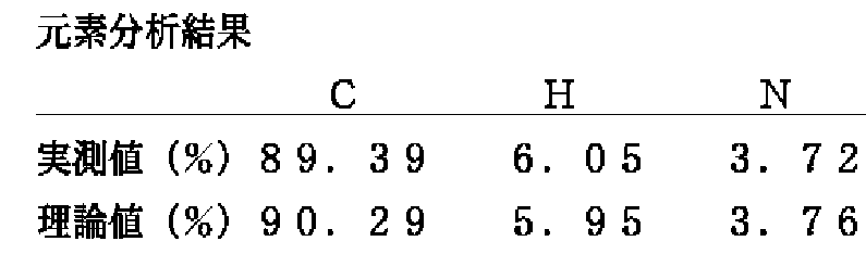
この化合物の融点は145〜148℃であり、元素分析結果は、下記のとおりである。
〔N,N′−ビス(4−イソプロピルフェニル)−N,N′−ビス(2−フェニル−1−プロペニル)−9,10−ジアミノフェナントレンの合成〕
式(1a-2):
【0055】
【化10】
で表されるN,N′−ビス(4−イソプロピルフェニル)−9,10−ジアミノフェナントレン3g(6.7ミリモル)と、式(1b-2):
【0057】
【化11】
で表される2−フェニルプロピオンアルデヒド1.9g(14.2ミリモル)と、ショウノウスルホン酸0.3g(1.3ミリモル)とを用いたこと以外は合成例1と同様にして、式(11-2):
【0059】
【化12】
で表される標記化合物2.6g(収率57%)をえた。
この化合物の融点は126〜129℃であり、元素分析結果は、下記のとおりである。
実施例1
電荷発生剤である、式(CG1) :
【0061】
【化13】
で表されるX型無金属フタロシアニン5重量部と、正孔輸送剤である、合成例1でえた、前記式(11-1)で表される化合物100重量部と、結着樹脂であるポリカーボネート100重量部とを、800重量部のテトラヒドロフランとともに、ボールミルにて50時間、混合し、分散させて単層型感光層用の塗布液を調整した。
【0063】
つぎにこの塗布液を、導電性基材であるアルミニウム素管上に、ディップコート法にて塗布し、110℃で30分間、熱風乾燥させて、膜厚25μmの単層型感光層を形成して、デジタル光源用の感光体を製造した。
実施例2
電荷発生剤として、X型無金属フタロシアニンに代えて、式(CG2) :
【0064】
【化14】
で表されるオキソチタニルフタロシアニン5重量部を使用したこと以外は実施例1と同様にして、単層型感光層を有するデジタル光源用の感光体を製造した。
実施例3、4
正孔輸送剤として、式(11-1)の化合物に代えて、合成例2でえた、前記式(11-2)で表される化合物100重量部を使用したこと以外は実施例1、2と同様にして、単層型感光層を有するデジタル光源用の感光体を製造した。
【0066】
比較例1、2
正孔輸送剤として、式(11-1)の化合物に代えて、前記一般式(2) で表される従来のビスエナミン化合物に属する、前述した特開平1−195455号公報に所載の、式(2-1) :
【0067】
【化15】
で表される化合物100重量部を使用したこと以外は実施例1、2と同様にして、単層型感光層を有するデジタル光源用の感光体を製造した。
比較例3、4
正孔輸送剤として、式(11-1)の化合物に代えて、前記一般式(2) で表される従来のビスエナミン化合物に属する、前述した特開平6−348045号公報に所載の、式(2-2) :
【0069】
【化16】
で表される化合物100重量部を使用したこと以外は実施例1、2と同様にして、単層型感光層を有するデジタル光源用の感光体を製造した。
比較例5、6
正孔輸送剤として、式(11-1)の化合物に代えて、前記一般式(2) で表される従来のビスエナミン化合物に属する、前述した特開平6−348045号公報に所載の、式(2-3) :
【0071】
【化17】
で表される化合物100重量部を使用したこと以外は実施例1、2と同様にして、単層型感光層を有するデジタル光源用の感光体を製造した。
上記各実施例、比較例の電子写真感光体について、下記の光感度試験Iを行い、その特性を評価した。
光感度試験I
ジェンテック(GENTEC)社製のドラム感度試験機を用いて、各実施例、比較例の電子写真感光体に印加電圧を加えて、その表面を+700±20Vに帯電させて、表面電位V0 (V)を測定した。
【0073】
つぎに、上記試験機の露光光源であるハロゲンランプの白色光から、バンドパスフィルターによって取り出した、波長780nm(半値幅20nm)、光強度10μJ/cm2 の単色光を、上記帯電状態の感光体の表面に照射(照射時間1.5秒)して、露光開始から0.5秒、経過した時点での表面電位を、残留電位Vr (V)として測定した。
【0074】
上記の残留電位Vr (V)が低いほど、感光体は高感度である。
結果を表1に示す。
【0075】
【表1】
《デジタル光源用感光体(単層型−電子輸送剤併用系)》
実施例5〜8、比較例7〜12
塗布液に、電子輸送剤である、式(ET1) :
【0077】
【化18】
で表される3,5−ジメチル−3′,5′−ジt−ブチル−4,4′−ジフェノキノン30重量部を添加したこと以外は実施例1〜4、比較例1〜6と同様にして、単層型感光層を有するデジタル光源用の感光体を製造した。
上記各実施例、比較例の電子写真感光体について、前記の光感度試験Iを行い、その特性を評価した。結果を表2に示す。
【0079】
【表2】
《アナログ光源用感光体(単層型)》
実施例9〜12
電荷発生剤として、X型無金属フタロシアニンに代えて、式(CG3) :
【0081】
【化19】
で表されるペリレン顔料5重量部、式(CG4) :
【0083】
【化20】
で表されるビスアゾ顔料5重量部、式(CG5) :
【0085】
【化21】
で表されるビスアゾ顔料5重量部、または式(CG6) :
【0087】
【化22】
で表されるビスアゾ顔料5重量部のいずれかを使用したこと以外は実施例1と同様にして、単層型感光層を有するアナログ光源用の感光体を製造した。
実施例13〜16
正孔輸送剤として、式(11-1)の化合物に代えて、合成例2でえた、前記式(11-2)で表される化合物100重量部を使用したこと以外は実施例9〜12と同様にして、単層型感光層を有するアナログ光源用の感光体を製造した。
【0089】
比較例13〜16
正孔輸送剤として、式(11-1)の化合物に代えて、前記式(2-1) で表される化合物100重量部を使用したこと以外は実施例9〜12と同様にして、単層型感光層を有するアナログ光源用の感光体を製造した。
比較例17〜20
正孔輸送剤として、式(11-1)の化合物に代えて、前記式(2-2) で表される化合物100重量部を使用したこと以外は実施例9〜12と同様にして、単層型感光層を有するアナログ光源用の感光体を製造した。
【0090】
比較例21〜24
正孔輸送剤として、式(11-1)の化合物に代えて、前記式(2-3) で表される化合物100重量部を使用したこと以外は実施例9〜12と同様にして、単層型感光層を有するアナログ光源用の感光体を製造した。
上記各実施例、比較例の電子写真感光体について、下記の光感度試験IIを行い、その特性を評価した。
【0091】
光感度試験II
ジェンテック(GENTEC)社製のドラム感度試験機を用いて、各実施例、比較例の電子写真感光体に印加電圧を加えて、その表面を+700±20Vに帯電させて、表面電位V0 (V)を測定した。
つぎに、上記試験機の露光光源であるハロゲンランプの白色光(光強度10ルックス)を、上記帯電状態の感光体の表面に照射(照射時間1.5秒)して、露光開始から0.5秒、経過した時点での表面電位を、残留電位Vr (V)として測定した。
【0092】
上記の残留電位Vr (V)が低いほど、感光体は高感度である。
結果を表3、4に示す。
【0093】
【表3】
【表4】
《アナログ光源用感光体(単層型−電子輸送剤併用系)》
実施例17〜24、比較例25〜36
塗布液に、電子輸送剤である、前記式(ET1) で表される3,5−ジメチル−3′,5′−ジt−ブチル−4,4′−ジフェノキノン30重量部を添加したこと以外は実施例9〜16、比較例13〜24と同様にして、単層型感光層を有するアナログ光源用の感光体を製造した。
【0096】
上記各実施例、比較例の電子写真感光体について、前記の光感度試験IIを行い、その特性を評価した。結果を表5、6に示す。
【0097】
【表5】
【表6】
《デジタル光源用感光体(積層型)》
実施例25
電荷発生剤である、前記式(CG1) で表されるX型無金属フタロシアニン2.5重量部と、結着樹脂であるポリビニルブチラール1重量部とを、15重量部のテトラヒドロフランとともに、ボールミルにて混合し、分散させて電荷発生層用の塗布液を調整した。
【0100】
つぎにこの塗布液を、導電性基材であるアルミニウム素管上に、ディップコート法にて塗布し、110℃で30分間、熱風乾燥させて、膜厚0.5μmの電荷発生層を形成した。
つぎに正孔輸送剤としての、合成例1でえた、前記式(11-1)で表される化合物1重量部と、結着樹脂であるポリカーボネート1重量部とを、10重量部のテトラヒドロフランとともに、ボールミルにて混合し、分散させて電荷輸送層用の塗布液を調整した。
【0101】
つぎにこの塗布液を、上記電荷発生層上に、ディップコート法にて塗布し、110℃で30分間、熱風乾燥させて、膜厚20μmの電荷輸送層を形成して、積層型感光層を有するデジタル光源用の感光体を製造した。
実施例26
電荷発生剤として、X型無金属フタロシアニンに代えて、前記式(CG2) で表されるオキソチタニルフタロシアニン2.5重量部を使用したこと以外は実施例25と同様にして、積層型感光層を有するデジタル光源用の感光体を製造した。
【0102】
実施例27、28
正孔輸送剤として、式(11-1)の化合物に代えて、合成例2でえた、前記式(11-2)で表される化合物1重量部を使用したこと以外は実施例25、26と同様にして、積層型感光層を有するデジタル光源用の感光体を製造した。
比較例37、38
正孔輸送剤として、式(11-1)の化合物に代えて、前記式(2-1) で表される化合物1重量部を使用したこと以外は実施例25、26と同様にして、積層型感光層を有するデジタル光源用の感光体を製造した。
【0103】
比較例39、40
正孔輸送剤として、式(11-1)の化合物に代えて、前記式(2-2) で表される化合物1重量部を使用したこと以外は実施例25、26と同様にして、積層型感光層を有するデジタル光源用の感光体を製造した。
比較例41、42
正孔輸送剤として、式(11-1)の化合物に代えて、前記式(2-3) で表される化合物1重量部を使用したこと以外は実施例25、26と同様にして、積層型感光層を有するデジタル光源用の感光体を製造した。
【0104】
上記各実施例、比較例の電子写真感光体について、下記の光感度試験III を行い、その特性を評価した。
光感度試験III
ジェンテック(GENTEC)社製のドラム感度試験機を用いて、各実施例、比較例の電子写真感光体に印加電圧を加えて、その表面を−700±20Vに帯電させて、表面電位V0 (V)を測定した。
【0105】
つぎに、上記試験機の露光光源であるハロゲンランプの白色光から、バンドパスフィルターによって取り出した、波長780nm(半値幅20nm)、光強度10μJ/cm2 の単色光を、上記帯電状態の感光体の表面に照射(照射時間1.5秒)して、露光開始から0.5秒、経過した時点での表面電位を、残留電位Vr (V)として測定した。
【0106】
上記の残留電位Vr (V)が低いほど、感光体は高感度である。
結果を表7に示す。
【0107】
【表7】
《アナログ光源用感光体(積層型)》
実施例29〜32
電荷発生剤として、X型無金属フタロシアニンに代えて、前記式(CG3) で表されるペリレン顔料2.5重量部、式(CG4) で表されるビスアゾ顔料2.5重量部、式(CG5) で表されるビスアゾ顔料2.5重量部、または式(CG6) で表されるビスアゾ顔料2.5重量部のいずれかを使用したこと以外は実施例25と同様にして、積層型感光層を有するアナログ光源用の感光体を製造した。
【0109】
実施例33〜36
正孔輸送剤として、式(11-1)の化合物に代えて、合成例2でえた、前記式(11-2)で表される化合物1重量部を使用したこと以外は実施例29〜32と同様にして、積層型感光層を有するアナログ光源用の感光体を製造した。
比較例43〜46
正孔輸送剤として、式(11-1)の化合物に代えて、前記式(2-1) で表される化合物1重量部を使用したこと以外は実施例29〜32と同様にして、積層型感光層を有するアナログ光源用の感光体を製造した。
【0110】
比較例47〜50
正孔輸送剤として、式(11-1)の化合物に代えて、前記式(2-2) で表される化合物1重量部を使用したこと以外は実施例29〜32と同様にして、積層型感光層を有するアナログ光源用の感光体を製造した。
比較例51〜54
正孔輸送剤として、式(11-1)の化合物に代えて、前記式(2-3) で表される化合物1重量部を使用したこと以外は実施例29〜32と同様にして、積層型感光層を有するアナログ光源用の感光体を製造した。
【0111】
上記各実施例、比較例の電子写真感光体について、下記の光感度試験IVを行い、その特性を評価した。
光感度試験IV
ジェンテック(GENTEC)社製のドラム感度試験機を用いて、各実施例、比較例の電子写真感光体に印加電圧を加えて、その表面を−700±20Vに帯電させて、表面電位V0 (V)を測定した。
【0112】
つぎに、上記試験機の露光光源であるハロゲンランプの白色光(光強度10ルックス)を、上記帯電状態の感光体の表面に照射(照射時間1.5秒)して、露光開始から0.5秒、経過した時点での表面電位を、残留電位Vr (V)として測定した。
上記の残留電位Vr (V)が低いほど、感光体は高感度である。
【0113】
結果を表8、9に示す。
【0114】
【表8】
【表9】
【発明の効果】
本発明のフェナントレンビスエナミン誘導体は、高い電荷輸送能、とくに正孔輸送能を有しているため、たとえば電子写真感光体や太陽電池、エレクトロルミネッセンス素子等における電荷輸送剤、とりわけ正孔輸送剤として好適に使用できる。
【0117】
また本発明の電子写真感光体は、上記のフェナントレンビスエナミン誘導体を含有する感光層を有するので高感度であり、静電式複写機やレーザープリンタ、普通紙ファクシミリ装置等の画像形成装置の高速化、高性能化に寄与するという特有の作用効果を奏する。[0001]
BACKGROUND OF THE INVENTION
The present invention relates to a novel compound suitably used as a charge transport agent, particularly a hole transport agent, for example in solar cells, electroluminescence elements, electrophotographic photoreceptors, and the like, and electrostatic copying machines and laser printers using the same The present invention relates to an electrophotographic photosensitive member used in an image forming apparatus such as a plain paper facsimile machine.
[0002]
[Prior art]
The electrophotographic photosensitive member using the above charge transporting agent includes, for example, a monolayer type photosensitive layer in which a charge transporting agent is contained in a binder resin together with a charge generating agent that generates a charge by light irradiation Alternatively, there are so-called organic photoreceptors (OPCs) such as those having a laminated type photosensitive layer including a charge transport layer containing a charge transport agent and a charge generation layer containing a charge generator.
[0003]
Such organic photoreceptors are easier to manufacture than inorganic photoreceptors using inorganic semiconductor materials, and have a wide range of options such as charge generators, charge transport agents, binder resins, etc. There is an advantage of being large.
Conventionally, various organic compounds such as a carbazole compound, an oxadiazole compound, a pyrazoline compound, a hydrazone compound, a stilbene compound, a phenylenediamine compound, and a benzidine compound are known as the charge transport agent. Among them, representative examples include m-phenylenediamine and any one of the 6-membered rings constituting the m-phenylenediamine molecule, such as a halogen atom, an alkyl group, an alkoxy group, an aryl group, a cyano group, and a nitro group. Examples thereof include derivatives substituted with groups and the like.
[0004]
[Problems to be solved by the invention]
The m-phenylenediamine and its derivatives have good solubility in solvents and compatibility with binder resins, and are excellent in charge transport capability, but are insufficiently stable, and are particularly reactive by light irradiation. When the singlet excited state is high, there is a problem that it easily deteriorates or decomposes.
[0005]
This is because electrons in the HOMO position related to hole transport (Highest Occupied Molecular Orbital) are localized at the 6th and 6th carbon atoms of the 6-membered ring located in the center of the molecule. This is because the chemical reactivity of this part is increased.
For this reason, for example, an electrophotographic photoreceptor using the above-described m-phenylenediamine or a derivative thereof as a charge transport agent is subjected to a photochemical reaction when the charge, exposure, and charge removal steps are repeated in the image forming apparatus. As a result, there is a problem that a deteriorated substance is generated, which causes a decrease in sensitivity of the photoreceptor and an increase in charge.
[0006]
Therefore, recently, as a new charge transporting agent, the general formula (2) having an enamine moiety in the molecule:
[0007]
[Chemical 3]
[In the formula, Ar represents an alkylene group, an arylene group, a divalent heterocyclic group, etc .;aRepresents an alkyl group, an aryl group or a heterocyclic group. RbAnd RcAre the same or different and each represents an alkyl group, an aryl group, an aralkyl group or a heterocyclic group, and RdRepresents a hydrogen atom or a lower alkyl group. Each of the above groups may have a substituent. The bis-enamine compound represented by these is proposed (Unexamined-Japanese-Patent No. 1-195455, Unexamined-Japanese-Patent No. 6-348045).
[0009]
The bis-enamine compound has an excellent charge transport capability as compared with the above-described conventional charge transport agent, and also has excellent stability, and is difficult to be degraded or decomposed by light irradiation. It is expected that the increase in charge can be suppressed.
However, as a result of investigations by the inventors, it has been clarified that the above bisenamine compound has room for further improvement.
[0010]
SUMMARY OF THE INVENTION An object of the present invention is to provide a novel compound that is further excellent in charge transport capability compared to conventional bisenamine compounds, and an electrophotographic photosensitive member that is highly sensitive and durable using the compound as a charge transport agent. There is.
[0011]
[Means for Solving the Problems]
In order to solve the above-mentioned problems, the inventors have conducted intensive research.As a result, Ar in the general formula (2) uses a phenanthrene ring that is not specifically disclosed in both publications. It has been found that when the enamine moiety is substituted at the 9-position and the 10-position, respectively, the charge transport ability can be specifically improved as compared with the conventional bis-enamine compounds disclosed in both publications, and the present invention has been completed.
[0012]
That is, the phenanthrenebisenamine derivative of the present invention has the general formula (1):
[0013]
[Formula 4]
[In the formula, R1A, R1BAnd RFourAre the same or different and each represents a hydrogen atom, an alkyl group, an alkoxy group, an aryl group or an aralkyl group, and R2A, R2B, R3AAnd R3BAre the same or different and each represents an alkyl group, an aryl group or an aralkyl group. Each of the above groups may have a substituent. a, b and c are the same or different and represent an integer of 1 to 3; When a, b or c is 2 or 3, each R1A, R1BAnd RFourMay be different.R 1A , R 1B , R 2A , R 2B , R 3A , R 3B And R Four Examples of the substituent which may be substituted for each group corresponding to are a halogen atom, an alkyl group, an alkoxy group, an aryl group or an aralkyl group. R 1A , R 1B , R 2A , R 2B , R 3A , R 3B And R Four Examples of the aryl group corresponding to and the aryl group as a substituent include a phenyl group, a tolyl group, a xylyl group, a biphenylyl group, an o-terphenyl group, a naphthyl group, an anthryl group, and a phenanthryl group.]
It is characterized by being represented by.
[0015]
Among the specific examples of the conventional bis-enamine compounds disclosed in both publications, those in which Ar in the general formula (2) is a benzene ring or a biphenyl ring are in the HOMO position as in the case of the m-phenylenediamine derivative described above. Electrons may be localized.
On the other hand, in the phenanthrenebisenamine derivative of the present invention represented by the general formula (1), the electrons at the HOMO position in the phenanthrene ring at the center of the molecule are not localized as described above and spread over the entire ring. Tend to delocalize.
[0016]
For this reason, the phenanthrenebisenamine derivative of the present invention has a larger range of existence of electrons at the HOMO position, coupled with the fact that the phenanthrene ring has a larger π-electron conjugated system than the benzene ring, naphthalene ring, biphenyl ring, etc. Therefore, the charge transfer is good and the charge transport ability is higher.
The phenanthrenebisenamine derivative of the present invention has a structure in which the enamine moiety is substituted at the 9-position and 10-position of the phenanthrene ring, respectively. Among the specific examples of the conventional bis-enamine compounds disclosed in both publications, In the general formula (2), since Ar has a stronger molecular asymmetry than those in which Ar is an anthracene ring or pyrene ring having the same size as the phenanthrene ring, the solubility in a solvent and the binder resin And is uniformly dispersed in the photosensitive layer, the charge hopping distance is short, and the charge transport property is excellent particularly in a low electric field.
[0017]
Further, as described above, the phenanthrenebisenamine derivative of the present invention in which electrons at the HOMO position are delocalized has a planar distribution of three-dimensional electrons. When the photosensitive layer is incorporated with a charge generating agent, the interaction with the charge generating agent, that is, the action of extracting charges (particularly holes) generated by the charge generating agent is strengthened, and the charge generating efficiency of the charge generating agent is increased. It also has a function of improving.
[0018]
Therefore, the phenanthrenebisenamine derivative of the present invention has an excellent function as a charge transport agent for an electrophotographic photoreceptor. In addition, the phenanthrenebisenamine derivative of the present invention can be used for applications such as solar cells and electroluminescent devices by utilizing its high charge transport ability.
The electrophotographic photoreceptor of the present invention is characterized in that a photosensitive layer containing a phenanthrenebisenamine derivative represented by the general formula (1) is provided on a conductive substrate, and has high sensitivity. .
[0019]
That is, the photosensitive layer containing the phenanthrenebisenamine derivative has excellent charge transport properties at a low electric field, and the ratio of recombination of electrons and holes in the layer is reduced, so that the apparent charge generation efficiency becomes an actual value. As a result, the sensitivity of the photoreceptor is improved. Further, the residual potential of the photosensitive member is lowered, and the stability and durability upon repeated exposure are improved.
[0020]
In particular, the phenanthrenebisenamine derivative is excellent in the action of extracting holes from the charge generating agent as described above, and does not cause interaction with the electron transporting agent that inhibits the transport of electrons and holes. When used as a hole transporting agent in a single-layer type photosensitive layer containing a charge generating agent and an electron transporting agent in the layer, a more sensitive photoreceptor can be constituted.
[0021]
DETAILED DESCRIPTION OF THE INVENTION
The present invention is described below.
First, the phenanthrenebisenamine derivative of the present invention will be described.
R in the general formula (1)1A, R1B, R2A, R2B, R3A, R3BAnd RFourExamples of the alkyl group corresponding to 1 include alkyl groups having 1 to 6 carbon atoms such as methyl, ethyl, normal propyl, isopropyl, normal butyl, isobutyl, secondary butyl, tertiary butyl, pentyl, hexyl and the like. Examples of the aryl group include phenyl, tolyl, xylyl, biphenylyl, o-terphenyl, naphthyl, anthryl, phenanthryl and the like. Examples of the aralkyl group include benzyl, benzhydryl, trityl, phenethyl and the like. In addition R1A, R1BAnd RFourExamples of the alkoxy group corresponding to are methoxy, ethoxy, normal propoxy, isopropoxy, tertiary butoxy, pentyloxy, hexyloxy and the like.
[0022]
Moreover, each group of the said alkyl group, an alkoxy group, an aryl group, and an aralkyl group may have a substituent, respectively. Examples of the substituent include halogen atoms such as fluorine, chlorine, bromine and iodine, the alkyl group, alkoxy group, aryl group and aralkyl group.
R1A, R1BAnd RFourA, b and c which are the same or different and represent an integer of 1 to 3, and when either a, b or c is 2 or 3, the corresponding group R1A, R1BAnd RFourMay be different. That is, R1AAs an example, when a is 2 or 3, 2 or 3 R substituted on the benzene ring1AMay be the same or different groups. Other groups R1BAnd RFourThe same applies to.
[0023]
Among the phenanthrenebisenamine derivatives of the present invention, the group R2AAnd R2BAre the same group R2And the group R3AAnd R3BAre the same group RThreeIn order to synthesize a phenanthrenebisenamine derivative represented by the following general formula (11), a phenanthrenediamine derivative represented by the general formula (1a) and a general formula (1b And an acetaldehyde derivative represented by the following formula in a suitable solvent, for example, in the presence of camphorsulfonic acid.
[0024]
[Chemical formula 5]
[In the formula, R1A, R1B, RFour, A, b and c are as defined above, and R2And RThreeR2A, R2B, R3AAnd R3BIt is the same. ]
Examples of the solvent used in the above reaction include toluene, xylene, acetic acid and the like, and the reaction is performed at 100 to 150 ° C. for about 2 to 6 hours.
In addition, the group R2AAnd R2BAre different from each other or the group R3AAnd R3BIn order to synthesize a phenanthrenebisenamine derivative in which is different from each other or both, one> NH group of the phenanthrenediamine derivative represented by the general formula (1a) is sealed by acetylation or the like In this state, after reacting with the acetaldehyde derivative represented by the general formula (1b), the above-mentioned sealing is released, and another kind of the group represented by the general formula (1b), that is, the group R2And / or RThreeMay be reacted with an acetaldehyde derivative different from the previous one.
[0026]
The phenanthrenediamine derivative represented by the general formula (1a) is, for example, a phenanthreneimine derivative produced by the reaction of an aniline derivative and a 9,10-phenanthrenequinone derivative described in JP-A-6-21757. May be synthesized by a method of reducing.
Specific examples of the phenanthrenebisenamine derivative of the present invention include, but are not limited to, for example, compounds represented by the formulas (11-1) to (11-2) belonging to the general formula (11). It is done.
[0027]
[Chemical 6]
Next, the electrophotographic photosensitive member of the present invention will be described.
The electrophotographic photoreceptor of the present invention is provided with a photosensitive layer containing one or more of the phenanthrenebisenamine derivatives of the present invention represented by the general formula (1) as a charge transport agent on a conductive substrate. It is a thing. The photosensitive layer includes a so-called single layer type photosensitive layer and a laminated type photosensitive layer, and the present invention can be applied to both of them.
[0029]
The single-layer type photosensitive layer is obtained by incorporating a phenanthrenebisenamine derivative (1), which is a charge transport agent, together with a charge generator in a binder resin. Such a single-layer type photosensitive layer can handle both positive and negative charges with a single structure, and has a simple layer structure and excellent productivity.
In addition, as described above, the monolayer type photosensitive layer using the above phenanthrenebisenamine derivative (1) as a hole transporting agent and an electron transporting agent excellent in electron transporting property allows the phenanthrenebisenamine derivative (1) to transport electrons. Since there is no interaction with the agent, the sensitivity is higher. In other words, even if both transport agents are contained in the same layer at a high concentration where hole transport and electron transport occur efficiently, a charge transfer complex is not formed in the layer, so the phenanthrenebisenamine derivative that is a hole transport agent ( 1) can transport holes efficiently, and the electron transport agent can transport electrons efficiently. As a result, the residual potential of the photoreceptor is greatly reduced and the sensitivity is improved.
[0030]
On the other hand, a multilayer photosensitive layer is formed by laminating a charge generation layer containing a charge generation agent and a charge transport layer containing a charge transfer agent in this order or in the reverse order on a conductive substrate. Is.
However, since the charge generation layer is much thinner than the charge transport layer, it is preferable to form a charge generation layer on a conductive substrate and to form a charge transport layer on the conductive base for protection. .
[0031]
Depending on the order of formation of the charge generation layer and the charge transport layer and the type of charge transport agent used in the charge transport layer, the laminate type photosensitive layer is selected as a positive or negative charge type.
For example, in the above-described layer structure in which a charge generation layer is formed on a conductive substrate and a charge transport layer is formed thereon, the charge transporting agent for the charge transport layer is the phenanthrenebisenamine derivative (1) of the present invention. When a positive hole transport agent is used, the photosensitive layer is a negatively charged type. In this case, the charge generation layer may contain an electron transport agent.
[0032]
On the other hand, in the above layer configuration, when an electron transport agent is used as the charge transport agent of the charge transport layer, the photosensitive layer is a positively charged type. In this case, the phenanthrenebisenamine derivative (1) of the present invention may be contained in the charge generation layer as a hole transport agent.
The charge generating agent, electron transporting agent and binder resin used in the electrophotographic photoreceptor of the present invention are as follows.
<Charge generator>
Examples of the charge generator include powders of inorganic photoconductive materials such as selenium, selenium-tellurium, selenium-arsenic, cadmium sulfide, α-silicon, or phthalocyanine pigments, perylene pigments, bisazo pigments, dithioketopyrrolopyrrole. Pigments, naphthalocyanine pigments, squaraine pigments, monoazo pigments, trisazo pigments, ansanthrone pigments, indigo pigments, azurenium pigments, cyanine pigments, triphenylmethane pigments, selenium pigments, toluidine pigments Examples thereof include pigments, pyrazoline pigments, quinacridone pigments, and pyrylium salts. These charge generating agents can be used alone or in combination of two or more according to the sensitivity region of the intended photoreceptor.
[0033]
Among the charge generators exemplified above, phthalocyanine pigments such as X-type metal-free phthalocyanine and oxotitanyl phthalocyanine, perylene pigments, bisazo pigments, and the like can be given.
Of these, phthalocyanine pigments are excellent in matching with the phenanthrenebisenamine derivative (1), and are highly sensitive to light in the wavelength region of 700 nm or more. Therefore, digital optics using a light source in the above wavelength region. It is suitably used for a system image forming apparatus.
[0034]
Both perylene pigments and bisazo pigments have excellent matching with the phenanthrenebisenamine derivative (1) and are highly sensitive to light in the visible region, and therefore use light sources in the above wavelength region. It is suitably used for an image forming apparatus of an analog optical system.
《Electron transport agent》
Examples of electron transporting agents include benzoquinone compounds, diphenoquinone compounds, naphthoquinone compounds, malononitrile, thiopyran compounds, tetracyanoethylene, tetracyanoquinodimethane, chloranil, bromoanil, 2,4,8-trinitrothioxanthone, and fluorenone. Compounds such as 2,4,7-trinitro-9-fluorenone, 2,4,7-trinitro-9-dicyanomethylenefluorenone, 2,4,5,7-tetranitroxanthone, 2,4,8- Trinitrothioxanthone, dinitrobenzene, dinitroanthracene, dinitroacridine, nitroanthraquinone, dinitroanthraquinone, succinic anhydride, maleic anhydride, dibromomaleic anhydride, 2,4,7-trinitrofluorenone imine compound Ethylated nitrofluorenone imine compound, tryptoanthrin compound, tryptoanthrin imine compound, azafluorenone compound, dinitropyridoquinazoline compound, thioxanthene compound, 2-phenyl-1,4-benzoquinone compound, 2-phenyl-1,4-naphthoquinone compounds, 5,12-naphthacenequinone compounds, α-cyanostilbene compounds, 4′-nitrostilbene compounds, salts of anion radicals and cations of benzoquinone compounds, etc. Of these, various electron-withdrawing compounds are preferably used. These may be used alone or in combination of two or more.
<Binder resin>
Examples of the binder resin include styrene-based polymers, styrene-butadiene copolymers, styrene-acrylonitrile copolymers, styrene-maleic acid copolymers, acrylic polymers, styrene-acrylic copolymers, polyethylene, and ethylene. -Vinyl acetate copolymer, chlorinated polyethylene, polyvinyl chloride, polypropylene, vinyl chloride-vinyl acetate copolymer, polyester, alkyd resin, polyamide, polyurethane, polycarbonate, polyarylate, polysulfone, diallyl phthalate resin, ketone resin, polyvinyl Thermoplastic resins such as butyral resin and polyether resin, silicone resin, epoxy resin, phenol resin, urea resin, melamine resin and other cross-linkable thermosetting resins, epoxy-acrylate, urethane-acrylate Etc. of the photocurable resin. These binder resins can be used alone or in combination of two or more.
《Hole transport agent》
In addition to the phenanthrenebisenamine derivative (1) of the present invention, other hole transport agents can be used in combination with the electrophotographic photoreceptor of the present invention.
[0035]
Examples of such hole transporting agents include benzidine compounds, phenylenediamine compounds, naphthylenediamine compounds, phenanthrylenediamine compounds, oxadiazole compounds [for example, 2,5-di (4-methylaminophenyl) -1,3,4-oxadiazole etc.], styryl compounds [eg 9- (4-diethylaminostyryl) anthracene etc.], carbazole compounds [eg poly-N-vinylcarbazole etc.], organic polysilane compounds, pyrazoline series Compounds [eg 1-phenyl-3- (p-dimethylaminophenyl) pyrazoline, etc.], hydrazone compounds, triphenylamine compounds, indole compounds, oxazole compounds, isoxazole compounds, thiazole compounds, thiadiazole compounds Imidazole compounds, pyrazole compounds, triazole compounds, butadiene compounds, pyrene-hydrazone compounds, acrolein compounds, carbazole-hydrazone compounds, quinoline-hydrazone compounds, stilbene compounds, stilbene hydrazone compounds, and di A phenylenediamine compound or the like is preferably used. These may be used alone or in combination of two or more.
[0036]
Next, a method for producing the electrophotographic photoreceptor of the present invention will be described.
In order to obtain an electrophotographic photosensitive member having a single-layer type photosensitive layer, the phenanthrenebisenamine derivative (1) of the present invention is used as a charge generator, a binder resin, and optionally an electron transport agent or other hole. A coating solution dissolved or dispersed in a suitable solvent together with a transport agent or the like may be applied on a conductive substrate by means of coating or the like and dried.
[0037]
In the single-layer type photosensitive layer, the charge generator is blended in an amount of 0.1 to 50 parts by weight, preferably 0.5 to 30 parts by weight with respect to 100 parts by weight of the binder resin, and the phenanthrene of the present invention. The hole transport agent containing the bisenamine derivative (1) is blended in an amount of 5 to 500 parts by weight, preferably 25 to 200 parts by weight. The electron transfer agent is blended in an amount of 5 to 100 parts by weight, preferably 10 to 80 parts by weight. Furthermore, the total amount of the hole transporting agent and the electron transporting agent is 20 to 500 parts by weight, preferably 30 to 200 parts by weight with respect to 100 parts by weight of the binder resin.
[0038]
The thickness of the single-layer type photosensitive layer is 5 to 100 μm, preferably 10 to 50 μm.
In order to obtain an electrophotographic photosensitive member having a photosensitive layer in which a charge generation layer is disposed on the lower side among the multilayer type photosensitive layers as described above, first, a charge generation layer is formed on a conductive substrate. A charge transport layer may be formed by applying a coating liquid containing a charge transport agent and a binder resin on the charge generation layer by means such as coating and drying.
[0039]
Among the laminated photosensitive layers, the charge generation layer includes a charge generation agent alone and a binder resin containing a charge generation agent. The former charge generation layer is a conductive substrate. It is formed by vapor-depositing a charge generating agent thereon or by applying and drying a coating solution containing the charge generating agent by means such as coating. The latter charge generation layer is formed by applying a coating solution containing a charge generating agent and a binder resin by means such as coating and drying.
[0040]
Among the above, in the resin binder type charge generation layer, the charge generator and the binder resin can be used in various ratios, but the charge generator is used with respect to 100 parts by weight of the binder resin. It is appropriate to add 5 to 1000 parts by weight, preferably 30 to 500 parts by weight.
The charge transport agent and the binder resin that constitute the charge transport layer laminated on the charge generation layer can be used in various proportions within a range that does not inhibit charge transport and a range that does not crystallize. So that the charge generated in the charge generation layer can be easily transported by 10 to 500 parts by weight, preferably 25 to 100 parts by weight, based on 100 parts by weight of the binder resin. is there.
[0041]
When the charge generating layer contains a charge transporting agent having the opposite transport property to that contained in the charge transporting layer, the charge transporting agent is added in an amount of 0.5 to 50 parts by weight with respect to 100 parts by weight of the binder resin. It is preferable to add 1 to 40 parts by weight.
The thickness of the laminated photosensitive layer is about 0.01 to 5 μm, preferably about 0.1 to 3 μm for the charge generation layer, and about 2 to 100 μm, preferably about 5 to 50 μm for the charge transport layer.
[0042]
In the case of a single layer type photoreceptor, between the conductive substrate and the photosensitive layer, and in the case of a multilayer type photoreceptor, between the conductive substrate and the charge generation layer, and between the conductive substrate and the charge transport layer. Alternatively, a barrier layer may be formed between the charge generation layer and the charge transport layer as long as the characteristics of the photoreceptor are not impaired. Further, a protective layer may be formed on the surface of the photoreceptor.
Each of the single layer type and multilayer type photosensitive layers has various additives known per se, such as an antioxidant, a radical scavenger, a singlet quencher, and an ultraviolet absorber, as long as the electrophotographic characteristics are not adversely affected. Deterioration preventing agents such as, softeners, plasticizers, surface modifiers, extenders, thickeners, dispersion stabilizers, waxes, acceptors, donors, and the like can be blended.
[0043]
In order to improve the sensitivity of the photosensitive layer, known sensitizers such as terphenyl, halonaphthoquinones, and acenaphthylene may be used in combination with the charge generator.
As the conductive substrate used in the photoreceptor of the present invention, various materials having conductivity can be used. For example, aluminum, iron, copper, tin, platinum, silver, vanadium, molybdenum, chromium, cadmium, Examples thereof include simple metals such as titanium, nickel, palladium, indium, stainless steel, and brass, plastic materials on which the above metals are vapor-deposited or laminated, glass coated with aluminum iodide, tin oxide, indium oxide, and the like.
[0044]
The conductive substrate may be any of a sheet shape, a drum shape, etc., and the substrate itself may be conductive or the surface of the substrate may be conductive. The conductive substrate is preferably one having sufficient mechanical strength when used.
The photosensitive layer in the present invention is produced by applying and drying a coating solution prepared by dissolving or dispersing the resin composition containing the above-described components in a solvent on a conductive substrate.
[0045]
That is, the charge generator, charge transport agent, binder resin and the like exemplified above are dispersed and mixed together with an appropriate solvent using a known method such as a roll mill, a ball mill, an attritor, a paint shaker, or an ultrasonic disperser. Then, a coating solution is prepared, and this may be applied and dried by a known means.
Various organic solvents can be used as a solvent for preparing the coating solution. For example, alcohols such as methanol, ethanol, isopropanol and butanol, aliphatic hydrocarbons such as n-hexane, octane and cyclohexane, benzene, Aromatic hydrocarbons such as toluene, xylene, halogenated hydrocarbons such as dichloromethane, dichloroethane, carbon tetrachloride, chlorobenzene, ethers such as dimethyl ether, diethyl ether, tetrahydrofuran, ethylene glycol dimethyl ether, diethylene glycol dimethyl ether, acetone, methyl ethyl ketone, cyclohexanone, etc. Ketones, esters such as ethyl acetate and methyl acetate, dimethylformaldehyde, dimethylformamide, dimethylsulfoxide and the like. These solvents can be used alone or in combination of two or more.
[0046]
Further, a surfactant, a leveling agent or the like may be used in order to improve the dispersibility of the charge transport agent or charge generator and the smoothness of the photosensitive layer surface.
As described above, since the phenanthrenebisenamine derivative of the present invention has excellent charge, particularly hole transport ability, an electrophotographic photoreceptor using this as a charge transport agent (hole transport agent) has high sensitivity. Therefore, when the photoreceptor of the present invention is used, it is possible to increase the speed and performance of an image forming apparatus such as an electrostatic copying machine.
[0047]
【Example】
Hereinafter, the present invention will be described with reference to examples.
《Phenanthrenebisenamine derivative》
Synthesis example 1
[Synthesis of N, N′-bis (4-methylphenyl) -N, N′-bis (2,2-diphenylvinyl) -9,10-diaminophenanthrene]
Formula (1a-1):
[0048]
[Chemical 7]
N, N′-bis (4-methylphenyl) -9,10-diaminophenanthrene 3 g (7.7 mmol) represented by the formula (1b-1):
[0050]
[Chemical 8]
2,2-diphenylacetaldehyde (3.2 g, 16.3 mmol) and camphorsulfonic acid (0.4 g, 1.7 mmol) were added to the flask together with 150 ml of toluene, and a Dean-Stark collector was added to the flask. Attach and react under reflux for 4 hours.
Next, the toluene layer was separated from the reaction solution, washed with water, dried over sodium sulfate, and then toluene was distilled off.
[0052]
The resulting residue is purified by silica gel column chromatography using a chloroform-hexane mixed solvent to obtain the formula (11-1):
[0053]
[Chemical 9]
3.7 g (yield 64%) of the title compound represented by
The melting point of this compound is 145 to 148 ° C., and the results of elemental analysis are as follows.
[Synthesis of N, N′-bis (4-isopropylphenyl) -N, N′-bis (2-phenyl-1-propenyl) -9,10-diaminophenanthrene]
Formula (1a-2):
[0055]
[Chemical Formula 10]
N, N′-bis (4-isopropylphenyl) -9,10-diaminophenanthrene represented by the formula (1b-2):
[0057]
Embedded image
In the same manner as in Synthesis Example 1, except that 1.9 g (14.2 mmol) of 2-phenylpropionaldehyde and 0.3 g (1.3 mmol) of camphorsulfonic acid were used, -2) :
[0059]
Embedded image
2.6 g (yield 57%) of the title compound represented by
The melting point of this compound is 126 to 129 ° C., and the results of elemental analysis are as follows.
Example 1
Charge generator, formula (CG1):
[0061]
Embedded image
5 parts by weight of an X-type metal-free phthalocyanine represented by the formula: 100 parts by weight of the compound represented by the formula (11-1) obtained in Synthesis Example 1 which is a hole transport agent, and a polycarbonate which is a binder resin 100 parts by weight was mixed with 800 parts by weight of tetrahydrofuran in a ball mill for 50 hours and dispersed to prepare a coating solution for a single-layer type photosensitive layer.
[0063]
Next, this coating solution is applied on an aluminum base tube, which is a conductive base material, by dip coating, and dried with hot air at 110 ° C. for 30 minutes to form a single-layer type photosensitive layer having a thickness of 25 μm. A photoconductor for a digital light source was manufactured.
Example 2
As a charge generating agent, instead of X-type metal-free phthalocyanine, the formula (CG2):
[0064]
Embedded image
A photoconductor for a digital light source having a single-layer type photosensitive layer was produced in the same manner as in Example 1 except that 5 parts by weight of oxotitanyl phthalocyanine represented by the following formula was used.
Examples 3 and 4
Examples 1 and 2 were used except that 100 parts by weight of the compound represented by Formula (11-2) obtained in Synthesis Example 2 was used instead of the compound of Formula (11-1) as the hole transport agent. In the same manner as above, a photoconductor for a digital light source having a single-layer type photosensitive layer was produced.
[0066]
Comparative Examples 1 and 2
As the hole transport agent, instead of the compound of the formula (11-1), the formula described in the above-mentioned JP-A-1-195455 belonging to the conventional bisenamine compound represented by the general formula (2) is used. (2-1):
[0067]
Embedded image
A photoconductor for a digital light source having a single-layer type photosensitive layer was produced in the same manner as in Examples 1 and 2 except that 100 parts by weight of the compound represented by formula (1) was used.
Comparative Examples 3 and 4
As the hole transport agent, instead of the compound of the formula (11-1), the formula described in JP-A-6-348045 described above, which belongs to the conventional bisenamine compound represented by the general formula (2) (2-2):
[0069]
Embedded image
A photoconductor for a digital light source having a single-layer type photosensitive layer was produced in the same manner as in Examples 1 and 2 except that 100 parts by weight of the compound represented by formula (1) was used.
Comparative Examples 5 and 6
As the hole transport agent, instead of the compound of the formula (11-1), the formula described in JP-A-6-348045 described above, which belongs to the conventional bisenamine compound represented by the general formula (2) (2-3):
[0071]
Embedded image
A photoconductor for a digital light source having a single-layer type photosensitive layer was produced in the same manner as in Examples 1 and 2 except that 100 parts by weight of the compound represented by formula (1) was used.
The electrophotographic photosensitive member of each of the above examples and comparative examples was subjected to the following photosensitivity test I, and its characteristics were evaluated.
Photosensitivity test I
Using a drum sensitivity tester manufactured by GENTEC, an applied voltage is applied to the electrophotographic photosensitive member of each example and comparative example, and the surface is charged to + 700 ± 20 V to obtain a surface potential V0(V) was measured.
[0073]
Next, it extracted from the white light of the halogen lamp which is an exposure light source of the said test machine with the band pass filter, the wavelength of 780 nm (half-value width of 20 nm), and light intensity of 10 microJ / cm.2Is applied to the surface of the charged photosensitive member (irradiation time: 1.5 seconds), and the surface potential at the time when 0.5 seconds have elapsed from the start of exposure is determined as the residual potential V.rMeasured as (V).
[0074]
The above residual potential VrThe lower the (V), the higher the sensitivity of the photoreceptor.
The results are shown in Table 1.
[0075]
[Table 1]
<Photosensitive body for digital light source (single layer type-electron transfer agent combined system)>
Examples 5-8, Comparative Examples 7-12
Formula (ET1), which is an electron transport agent, in the coating solution:
[0077]
Embedded image
In the same manner as in Examples 1 to 4 and Comparative Examples 1 to 6, except that 30 parts by weight of 3,5-dimethyl-3 ', 5'-di-t-butyl-4,4'-diphenoquinone represented by Thus, a photoconductor for a digital light source having a single-layer type photosensitive layer was produced.
The electrophotographic photosensitive members of the above Examples and Comparative Examples were subjected to the above-mentioned photosensitivity test I, and their characteristics were evaluated. The results are shown in Table 2.
[0079]
[Table 2]
《Photosensitive body for analog light source (single layer type)》
Examples 9-12
As a charge generating agent, instead of X-type metal-free phthalocyanine, the formula (CG3):
[0081]
Embedded image
5 parts by weight of a perylene pigment represented by the formula (CG4):
[0083]
Embedded image
5 parts by weight of a bisazo pigment represented by the formula (CG5):
[0085]
Embedded image
5 parts by weight of a bisazo pigment represented by the formula (CG6):
[0087]
Embedded image
A photoconductor for an analog light source having a single-layer type photosensitive layer was produced in the same manner as in Example 1 except that any one of 5 parts by weight of a bisazo pigment represented by the following formula was used.
Examples 13-16
Examples 9 to 12 except that 100 parts by weight of the compound represented by the formula (11-2) obtained in Synthesis Example 2 was used as the hole transporting agent instead of the compound of the formula (11-1). In the same manner as above, a photoreceptor for an analog light source having a single-layer type photosensitive layer was produced.
[0089]
Comparative Examples 13-16
In the same manner as in Examples 9 to 12, except that 100 parts by weight of the compound represented by the formula (2-1) was used instead of the compound of the formula (11-1) as the hole transport agent. A photoconductor for an analog light source having a layer type photosensitive layer was produced.
Comparative Examples 17-20
In the same manner as in Examples 9 to 12, except that 100 parts by weight of the compound represented by the formula (2-2) was used instead of the compound of the formula (11-1) as the hole transport agent. A photoconductor for an analog light source having a layer type photosensitive layer was produced.
[0090]
Comparative Examples 21-24
In the same manner as in Examples 9 to 12, except that 100 parts by weight of the compound represented by the formula (2-3) was used in place of the compound of the formula (11-1) as the hole transport agent. A photoconductor for an analog light source having a layer type photosensitive layer was produced.
The electrophotographic photosensitive member of each of the above Examples and Comparative Examples was subjected to the following photosensitivity test II, and its characteristics were evaluated.
[0091]
Photosensitivity test II
Using a drum sensitivity tester manufactured by GENTEC, an applied voltage is applied to the electrophotographic photosensitive member of each example and comparative example, and the surface is charged to + 700 ± 20 V to obtain a surface potential V0(V) was measured.
Next, the surface of the charged photoconductor is irradiated with white light (light intensity 10 lux) of a halogen lamp which is an exposure light source of the test machine (irradiation time 1.5 seconds). The surface potential at the time when 5 seconds have elapsed is expressed as residual potential VrMeasured as (V).
[0092]
The above residual potential VrThe lower the (V), the higher the sensitivity of the photoreceptor.
The results are shown in Tables 3 and 4.
[0093]
[Table 3]
[Table 4]
<< Photoconductor for analog light source (single layer type-electron transport agent combined system) >>
Examples 17-24, Comparative Examples 25-36
Other than adding 30 parts by weight of 3,5-dimethyl-3 ', 5'-di-t-butyl-4,4'-diphenoquinone represented by the above formula (ET1), which is an electron transport agent, to the coating solution Were manufactured in the same manner as in Examples 9 to 16 and Comparative Examples 13 to 24, and a photoconductor for an analog light source having a single-layer type photosensitive layer was produced.
[0096]
The electrophotographic photosensitive member of each of the above Examples and Comparative Examples was subjected to the above-described photosensitivity test II, and the characteristics thereof were evaluated. The results are shown in Tables 5 and 6.
[0097]
[Table 5]
[Table 6]
<< Photosensitive body for digital light source (stacked type) >>
Example 25
In a ball mill, 2.5 parts by weight of an X-type metal-free phthalocyanine represented by the above formula (CG1) which is a charge generating agent and 1 part by weight of polyvinyl butyral which is a binder resin are mixed with 15 parts by weight of tetrahydrofuran. A coating solution for the charge generation layer was prepared by mixing and dispersing.
[0100]
Next, this coating solution was applied on an aluminum base tube, which is a conductive base material, by a dip coating method and dried with hot air at 110 ° C. for 30 minutes to form a charge generation layer having a thickness of 0.5 μm. .
Next, 1 part by weight of the compound represented by the formula (11-1) obtained in Synthesis Example 1 as a hole transporting agent and 1 part by weight of polycarbonate as a binder resin are mixed with 10 parts by weight of tetrahydrofuran. Then, they were mixed by a ball mill and dispersed to prepare a coating solution for the charge transport layer.
[0101]
Next, this coating solution is applied onto the charge generation layer by a dip coating method and dried with hot air at 110 ° C. for 30 minutes to form a charge transport layer having a thickness of 20 μm. A photoconductor for a digital light source was produced.
Example 26
In the same manner as in Example 25 except that 2.5 parts by weight of oxotitanyl phthalocyanine represented by the above formula (CG2) was used in place of X-type metal-free phthalocyanine as a charge generating agent, a laminated photosensitive layer was prepared. A photoconductor for a digital light source was produced.
[0102]
Examples 27 and 28
Examples 25 and 26 except that 1 part by weight of the compound represented by the formula (11-2) obtained in Synthesis Example 2 was used as the hole transport agent instead of the compound of the formula (11-1). In the same manner as described above, a photoconductor for a digital light source having a laminated photosensitive layer was produced.
Comparative Examples 37 and 38
In the same manner as in Examples 25 and 26, except that 1 part by weight of the compound represented by the formula (2-1) was used instead of the compound of the formula (11-1) as the hole transporting agent, A photoconductor for a digital light source having a mold type photosensitive layer was produced.
[0103]
Comparative Examples 39 and 40
Lamination was conducted in the same manner as in Examples 25 and 26 except that 1 part by weight of the compound represented by the formula (2-2) was used instead of the compound of the formula (11-1) as the hole transporting agent. A photoconductor for a digital light source having a mold type photosensitive layer was produced.
Comparative Examples 41 and 42
Lamination was conducted in the same manner as in Examples 25 and 26 except that 1 part by weight of the compound represented by the formula (2-3) was used instead of the compound of the formula (11-1) as the hole transport agent. A photoconductor for a digital light source having a mold type photosensitive layer was produced.
[0104]
The electrophotographic photoreceptors of the above examples and comparative examples were subjected to the following photosensitivity test III, and their characteristics were evaluated.
Photosensitivity test III
Using a drum sensitivity tester manufactured by GENTEC, an applied voltage is applied to the electrophotographic photosensitive member of each example and comparative example, and the surface is charged to −700 ± 20 V to obtain a surface potential V0(V) was measured.
[0105]
Next, it extracted from the white light of the halogen lamp which is an exposure light source of the said test machine with the band pass filter, the wavelength of 780 nm (half-value width of 20 nm), and light intensity of 10 microJ / cm.2Is applied to the surface of the charged photosensitive member (irradiation time: 1.5 seconds), and the surface potential at the time when 0.5 seconds have elapsed from the start of exposure is determined as the residual potential V.rMeasured as (V).
[0106]
The above residual potential VrThe lower the (V), the higher the sensitivity of the photoreceptor.
The results are shown in Table 7.
[0107]
[Table 7]
<< A photoreceptor for analog light source (stacked type) >>
Examples 29-32
As a charge generating agent, instead of X-type metal-free phthalocyanine, 2.5 parts by weight of a perylene pigment represented by the formula (CG3), 2.5 parts by weight of a bisazo pigment represented by the formula (CG4), a formula (CG5 A laminated photosensitive layer in the same manner as in Example 25 except that either 2.5 parts by weight of a bisazo pigment represented by formula (2.5) or 2.5 parts by weight of a bisazo pigment represented by formula (CG6) was used. A photoconductor for an analog light source having
[0109]
Examples 33-36
Examples 29-32 except that 1 part by weight of the compound represented by the formula (11-2) obtained in Synthesis Example 2 was used as the hole transport agent instead of the compound of the formula (11-1). In the same manner as above, a photoconductor for an analog light source having a laminated photosensitive layer was produced.
Comparative Examples 43-46
In the same manner as in Examples 29 to 32 except that 1 part by weight of the compound represented by the formula (2-1) was used instead of the compound of the formula (11-1) as a hole transporting agent, A photoconductor for an analog light source having a mold type photosensitive layer was produced.
[0110]
Comparative Examples 47-50
In the same manner as in Examples 29 to 32 except that 1 part by weight of the compound represented by the formula (2-2) was used instead of the compound of the formula (11-1) as the hole transporting agent, A photoconductor for an analog light source having a mold type photosensitive layer was produced.
Comparative Examples 51-54
Lamination was carried out in the same manner as in Examples 29 to 32 except that 1 part by weight of the compound represented by the formula (2-3) was used instead of the compound of the formula (11-1) as the hole transport agent. A photoconductor for an analog light source having a mold type photosensitive layer was produced.
[0111]
The electrophotographic photoreceptors of the above examples and comparative examples were subjected to the following photosensitivity test IV, and the characteristics thereof were evaluated.
Photosensitivity test IV
Using a drum sensitivity tester manufactured by GENTEC, an applied voltage is applied to the electrophotographic photosensitive member of each example and comparative example, and the surface is charged to −700 ± 20 V to obtain a surface potential V0(V) was measured.
[0112]
Next, the surface of the charged photoconductor is irradiated with white light (light intensity 10 lux) of a halogen lamp which is an exposure light source of the test machine (irradiation time 1.5 seconds). The surface potential at the time when 5 seconds have elapsed is expressed as residual potential VrMeasured as (V).
The above residual potential VrThe lower the (V), the higher the sensitivity of the photoreceptor.
[0113]
The results are shown in Tables 8 and 9.
[0114]
[Table 8]
[Table 9]
【The invention's effect】
The phenanthrenebisenamine derivative of the present invention has a high charge transporting ability, particularly a hole transporting ability. It can be used suitably.
[0117]
The electrophotographic photosensitive member of the present invention has a photosensitive layer containing the above-described phenanthrenebisenamine derivative, so that the electrophotographic photosensitive member has high sensitivity and speeds up image forming apparatuses such as electrostatic copying machines, laser printers, and plain paper facsimile machines. It has a unique effect of contributing to high performance.
Claims (3)
で表されることを特徴とするフェナントレンビスエナミン誘導体。General formula (1):
A phenanthrenebisenamine derivative characterized by being represented by:
で表されるフェナントレンビスエナミン誘導体を含む感光層を設けたことを特徴とする電子写真感光体。On the conductive substrate, the general formula (1):
An electrophotographic photosensitive member provided with a photosensitive layer containing a phenanthrenebisenamine derivative represented by the formula:
Priority Applications (1)
| Application Number | Priority Date | Filing Date | Title |
|---|---|---|---|
| JP13725396A JP3641069B2 (en) | 1996-05-30 | 1996-05-30 | Phenanthrenebisenamine derivative and electrophotographic photoreceptor using the same |
Applications Claiming Priority (1)
| Application Number | Priority Date | Filing Date | Title |
|---|---|---|---|
| JP13725396A JP3641069B2 (en) | 1996-05-30 | 1996-05-30 | Phenanthrenebisenamine derivative and electrophotographic photoreceptor using the same |
Publications (2)
| Publication Number | Publication Date |
|---|---|
| JPH09316039A JPH09316039A (en) | 1997-12-09 |
| JP3641069B2 true JP3641069B2 (en) | 2005-04-20 |
Family
ID=15194348
Family Applications (1)
| Application Number | Title | Priority Date | Filing Date |
|---|---|---|---|
| JP13725396A Expired - Lifetime JP3641069B2 (en) | 1996-05-30 | 1996-05-30 | Phenanthrenebisenamine derivative and electrophotographic photoreceptor using the same |
Country Status (1)
| Country | Link |
|---|---|
| JP (1) | JP3641069B2 (en) |
-
1996
- 1996-05-30 JP JP13725396A patent/JP3641069B2/en not_active Expired - Lifetime
Also Published As
| Publication number | Publication date |
|---|---|
| JPH09316039A (en) | 1997-12-09 |
Similar Documents
| Publication | Publication Date | Title |
|---|---|---|
| JP3641069B2 (en) | Phenanthrenebisenamine derivative and electrophotographic photoreceptor using the same | |
| JPH08151372A (en) | Bisoxadiazole derivative and photographic photoreceptor using the same | |
| JP3250959B2 (en) | Diazanaphtho [2,3-b] fluorene derivative and electrophotographic photoreceptor using the same | |
| JP3589796B2 (en) | Electrophotographic photoreceptor | |
| JP3618911B2 (en) | Dioxatetracenedione derivative | |
| JP3653464B2 (en) | Electrophotographic photoreceptor | |
| JP3805193B2 (en) | Stilbene derivative and electrophotographic photoreceptor using the same | |
| JP3448411B2 (en) | Tryptoanthrinimine derivatives and electrophotographic photoreceptors using the same | |
| JP3524994B2 (en) | Tryptoantrine derivative and electrophotographic photoreceptor | |
| JP3641068B2 (en) | Enamine derivative and electrophotographic photoreceptor using the same | |
| JP3670481B2 (en) | Electrophotographic photoreceptor using phenoxy derivatives | |
| JP3608877B2 (en) | Quinone derivative and electrophotographic photoreceptor using the same | |
| JP3694562B2 (en) | Dienamine derivative and electrophotographic photoreceptor using the same | |
| JP4767712B2 (en) | Triarylamine derivative, process for producing the same and electrophotographic photoreceptor | |
| JP3530650B2 (en) | Electrophotographic photoreceptor | |
| JPH07309824A (en) | Trinitrofluorenone imine derivative and electrophotographic receptor | |
| JPH0940644A (en) | Isatin derivative and electrophotographic photoreceptor using the same | |
| JPH11305457A (en) | Electrophotographic photoreceptor using phenylbenzofuranone derivative | |
| JPH11305456A (en) | Electrophotographic photoreceptor using phenylbenzodifuranone derivative | |
| JPH05992A (en) | Quinone compound and light sensitizer for electrophotography | |
| JPH08151381A (en) | Bisoxadiazole derivative and electrophotographic receptor using the same | |
| JPH0977763A (en) | Dioxotetracenedione derivative and electrophotographic receptor produced by using the derivative | |
| JPH08151371A (en) | Oxadiazole derivative and photographic photoreceptor using the same | |
| JP2007217357A (en) | Triarylamine derivative and method for producing the same and electrographic photosensitizer | |
| JPH08295659A (en) | Trinitrofluorenoneimine derivative and electrophotographic sensitizer using the same |
Legal Events
| Date | Code | Title | Description |
|---|---|---|---|
| A131 | Notification of reasons for refusal |
Free format text: JAPANESE INTERMEDIATE CODE: A131 Effective date: 20040804 |
|
| A521 | Request for written amendment filed |
Free format text: JAPANESE INTERMEDIATE CODE: A523 Effective date: 20040928 |
|
| TRDD | Decision of grant or rejection written | ||
| A01 | Written decision to grant a patent or to grant a registration (utility model) |
Free format text: JAPANESE INTERMEDIATE CODE: A01 Effective date: 20050106 |
|
| A61 | First payment of annual fees (during grant procedure) |
Free format text: JAPANESE INTERMEDIATE CODE: A61 Effective date: 20050120 |
|
| R150 | Certificate of patent or registration of utility model |
Free format text: JAPANESE INTERMEDIATE CODE: R150 |
|
| FPAY | Renewal fee payment (event date is renewal date of database) |
Free format text: PAYMENT UNTIL: 20090128 Year of fee payment: 4 |
|
| FPAY | Renewal fee payment (event date is renewal date of database) |
Free format text: PAYMENT UNTIL: 20090128 Year of fee payment: 4 |
|
| FPAY | Renewal fee payment (event date is renewal date of database) |
Free format text: PAYMENT UNTIL: 20100128 Year of fee payment: 5 |
|
| FPAY | Renewal fee payment (event date is renewal date of database) |
Free format text: PAYMENT UNTIL: 20100128 Year of fee payment: 5 |
|
| FPAY | Renewal fee payment (event date is renewal date of database) |
Free format text: PAYMENT UNTIL: 20110128 Year of fee payment: 6 |
|
| FPAY | Renewal fee payment (event date is renewal date of database) |
Free format text: PAYMENT UNTIL: 20120128 Year of fee payment: 7 |
|
| FPAY | Renewal fee payment (event date is renewal date of database) |
Free format text: PAYMENT UNTIL: 20130128 Year of fee payment: 8 |
|
| FPAY | Renewal fee payment (event date is renewal date of database) |
Free format text: PAYMENT UNTIL: 20130128 Year of fee payment: 8 |
|
| S533 | Written request for registration of change of name |
Free format text: JAPANESE INTERMEDIATE CODE: R313533 |
|
| FPAY | Renewal fee payment (event date is renewal date of database) |
Free format text: PAYMENT UNTIL: 20130128 Year of fee payment: 8 |
|
| R350 | Written notification of registration of transfer |
Free format text: JAPANESE INTERMEDIATE CODE: R350 |
|
| FPAY | Renewal fee payment (event date is renewal date of database) |
Free format text: PAYMENT UNTIL: 20130128 Year of fee payment: 8 |
|
| FPAY | Renewal fee payment (event date is renewal date of database) |
Free format text: PAYMENT UNTIL: 20140128 Year of fee payment: 9 |
|
| EXPY | Cancellation because of completion of term |