JP3636397B2 - Jitter suppression circuit - Google Patents
Jitter suppression circuit Download PDFInfo
- Publication number
- JP3636397B2 JP3636397B2 JP08260996A JP8260996A JP3636397B2 JP 3636397 B2 JP3636397 B2 JP 3636397B2 JP 08260996 A JP08260996 A JP 08260996A JP 8260996 A JP8260996 A JP 8260996A JP 3636397 B2 JP3636397 B2 JP 3636397B2
- Authority
- JP
- Japan
- Prior art keywords
- phase
- signal
- jitter
- phase difference
- signal point
- Prior art date
- Legal status (The legal status is an assumption and is not a legal conclusion. Google has not performed a legal analysis and makes no representation as to the accuracy of the status listed.)
- Expired - Fee Related
Links
Images


Classifications
-
- H—ELECTRICITY
- H04—ELECTRIC COMMUNICATION TECHNIQUE
- H04L—TRANSMISSION OF DIGITAL INFORMATION, e.g. TELEGRAPHIC COMMUNICATION
- H04L7/00—Arrangements for synchronising receiver with transmitter
- H04L7/0054—Detection of the synchronisation error by features other than the received signal transition
- H04L7/0062—Detection of the synchronisation error by features other than the received signal transition detection of error based on data decision error, e.g. Mueller type detection
-
- H—ELECTRICITY
- H04—ELECTRIC COMMUNICATION TECHNIQUE
- H04L—TRANSMISSION OF DIGITAL INFORMATION, e.g. TELEGRAPHIC COMMUNICATION
- H04L27/00—Modulated-carrier systems
- H04L27/32—Carrier systems characterised by combinations of two or more of the types covered by groups H04L27/02, H04L27/10, H04L27/18 or H04L27/26
- H04L27/34—Amplitude- and phase-modulated carrier systems, e.g. quadrature-amplitude modulated carrier systems
- H04L27/38—Demodulator circuits; Receiver circuits
- H04L27/3818—Demodulator circuits; Receiver circuits using coherent demodulation, i.e. using one or more nominally phase synchronous carriers
- H04L27/3827—Demodulator circuits; Receiver circuits using coherent demodulation, i.e. using one or more nominally phase synchronous carriers in which the carrier is recovered using only the demodulated baseband signals
Landscapes
- Engineering & Computer Science (AREA)
- Computer Networks & Wireless Communication (AREA)
- Signal Processing (AREA)
- Digital Transmission Methods That Use Modulated Carrier Waves (AREA)
Description
【0001】
【発明の属する技術分野】
本発明は、ジッタ抑圧回路に関し、特に、多重無線装置やCATV等に使用される多値直交振幅変調(QAM)方式の変調装置または復調装置で発生するジッタを抑圧するジッタ抑圧回路に関する。
【0002】
多重無線装置やCATV等に使用される多値直交振幅変調方式の送信装置や受信装置を小型化、低コスト化したいという要求がある。特に、周波数変換部において小型化、低コスト化を実現した場合、局部発振器の発振周波数精度が低下する場合が多く、これにより搬送波の劣化が発生する。この搬送波の劣化は、キャリアジッタ(以下、単にジッタと呼ぶ)と呼ばれ、搬送波が時間的に変動するものである。このジッタは、回線品質を低下させる原因となり、QAMの多値数が増大する程、影響が大きい。本発明は、ジッタを抑圧するジッタ抑圧回路に関する。
【0003】
【従来の技術】
従来のジッタ抑圧回路として、例えば図13に示すような復調回路に適用した回路がある。図中、復調回路では、ミキサ部(MIX)11が、変調波(DEM)に対して直交検波を行い、I相信号およびQ相信号をロールオフフィルタ12,13へそれぞれ出力する。ロールオフフィルタ12,13は、I相信号およびQ相信号の波形成形をそれぞれ行う。搬送波再生制御部(CR/CONT)14は、波形成形されたI相信号およびQ相信号を基に、再生搬送波の位相誤差を検出し、ローパスフィルタ15がその位相誤差から低周波成分を抽出して電圧制御発振器16へ送る。電圧制御発振器16は、ローパスフィルタ15の出力に応じた周波数の搬送波を再生し、ミキサ部11へ供給する。
【0004】
ジッタ抑圧回路では、制御部(CONT)17が、復調回路から送られたジッタを含むI相信号およびQ相信号を基に、これらのI相信号およびQ相信号が表す信号点を求め、この信号点と、この信号点に最も近い本来の信号点(理想信号点)との位相差θを検出する。積分器18は、制御部17で検出された位相差θの時間積分を行って、ノイズ成分を取り除き、位相差Θとして移相器21へ送る。
【0005】
移相器21の前には所定時間の遅延を行う遅延器19,20が設けられ、復調回路から送られたジッタを含むI相信号およびQ相信号に対して所定時間の遅延が行なわれる。その上で、移相器21が、積分器18から出力された位相差Θだけ、I相信号およびQ相信号が表す信号点の位相に対して位相補正を行う。この位相補正がジッタの抑圧となる。
【0006】
この位相補正として、移相器21では、下記式(1a),(1b)の演算を行う。
【0007】
【数1】
I0 =II × cosΘ−QI × sinΘ ・・・(1a)
Q0 =QI × cosΘ+II × sinΘ ・・・(1b)
ここで、II ,QI は、移相器21へ入力されるジッタ抑圧前のI相信号およびQ相信号を示し、I0 ,Q0 は、移相器21から出力されたジッタ抑圧後のI相信号およびQ相信号を示す。
【0008】
図14に、上記演算をハードウェアで実現する場合の移相器21の内部構成を示す。図中、ROM30は、アドレスΘのデータ格納場所に、データ cosΘおよび sinΘを格納するメモリであり、積分器18から位相差Θを受けると、そのΘに応じた cosΘおよび sinΘを出力する。データ cosΘは乗算器31,34へ送られ、データ sinΘは乗算器33,36へ送られる。移相器21へ入力されたジッタ抑圧前のI相信号(II )は、乗算器31,36へ送られ、移相器21へ入力されたジッタ抑圧前のQ相信号(QI )は、乗算器34,33へ送られる。そして、乗算器31の積値は減算器32へ送られ、乗算器33の積値も減算器32へ送られ、減算器32は、乗算器31からの積値から、乗算器33からの積値を減算して差を求め、ジッタ抑圧後のI相信号(I0 )として出力する。同様に、乗算器34の積値は加算器35へ送られ、乗算器36の積値も加算器35へ送られ、加算器35は、両積値の和を求め、ジッタ抑圧後のQ相信号(Q0 )として出力する。
【0009】
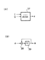
図15(A)は制御部17の内部構成を示す。すなわち、制御部17はROM37で構成され、ROM37では、復調回路から送られたジッタを含むI相信号およびQ相信号に対応する2次元のアドレスのデータ格納場所に、これらのアドレスの値に対応する信号点と、この信号点に最も近い本来の信号点(理想信号点)との位相差θのデータが格納されている。
【0010】
なお、制御部17を演算装置で構成し、下記式(2)に基づき位相差θを算出するようにしてもよい。
【0011】
【数2】
θ= tan-1(Q/I)− tan-1(Q’/I’) ・・・(2)
ここで、Q,Iは、復調回路から送られたジッタを含むI相信号およびQ相信号を示し、Q’,I’は、これらのジッタを含むI相信号およびQ相信号が表す信号点に最も近い本来の信号点(理想信号点)を表すI相信号およびQ相信号である。
【0012】
図15(B)は積分器18の内部構成を示す。すなわち、積分器18は、加算器38とフリップフロップ(FF)39とから成るアキュムレータであり、1シンボル前の演算結果に、新たに入力した位相差θを順次加算する。かくして、制御部17から送られた位相差θを積分して位相差Θとして移相器21へ出力する。
【0013】
このように、ジッタ抑圧回路は、移相器21の前側で検出した位相差Θに従って移相器21を作動させるフィードフォワード制御であるので、ジッタのような時間変動が高速なものに追従が可能である。
【0014】
【発明が解決しようとする課題】
ここで、この従来の復調回路が、図16に示すような64QAMの信号を扱っていると仮定する。そして、本来、信号点位置P1にあるべき信号点が、ジッタのために信号点位置P2にあったとする。その場合、ジッタ抑圧回路では、信号点位置P2に最も近い理想信号点の信号点位置P1を探し、その理想信号点位置P1からの位相差θ1を検出するようにする。そして、この位相差θ1を基にしてジッタの抑圧が行われ、信号点位置P2が理想信号点の信号点位置P1に移動される。
【0015】
しかし、ジッタが大きくなって、本来、信号点位置P1にあるべき信号点が信号点位置P3に位置した場合には、他の理想信号点の信号点位置P4が、信号点位置P3に最も近くなり、そのため、本来ならば位相差θ2が検出されるべきところを、ジッタ抑圧回路は、理想信号点の信号点位置P4からの位相差θ3を検出してしまい、この位相差θ3を基にしてジッタの抑圧が行われる。そのため、ジッタが減少するどころか、かえってジッタが増大してしまうとともに、ビットエラーを招いてしまうという問題点があった。
【0016】
本発明はこのような点に鑑みてなされたものであり、ジッタ量が増大してもジッタの正確な抑圧を可能にしたジッタ抑圧回路を提供することを目的とする。
【0017】
【課題を解決するための手段】
本発明では上記目的を達成するために、図1に示すように、ジッタを含むI相信号およびQ相信号を基に、当該I相信号およびQ相信号が表す信号点を求め、当該信号点と、当該信号点に最も近い理想信号点との位相差を検出する位相差検出手段1と、上記の理想信号点が所定の信号点群に属している信号点であるか否かを判定する判定手段2と、判定手段2の判定結果が肯定であるときに、位相差検出手段1で検出された位相差に基づいて、上記のジッタを含むI相信号およびQ相信号が表す信号点の位相補正を行う位相補正手段3とを有することを特徴とするジッタ抑圧回路が提供される。
【0018】
以上のような構成において、まず、位相差検出手段1が、入力されたジッタを含むI相信号およびQ相信号を基に、当該I相信号およびQ相信号が表す信号点を求め、当該信号点と、当該信号点に最も近い理想信号点との位相差を検出する。一方、判定手段2が、上記の理想信号点が所定の信号点群に属している信号点であるか否かを判定する。すなわち、信号点配置の直交座標において、振幅が同一で、互いの位相差が大きい理想信号点グループを、所定の信号点群に設定する。そして、今回入力のI相信号およびQ相信号が表す信号点に最も近い理想信号点が、こうした所定の信号点群に属している場合には、判定手段2は、判定結果が肯定である旨を位相補正手段3へ知らせる。判定結果が肯定である場合、隣接理想信号点どうしが比較的離れているので、今回入力のI相信号およびQ相信号が表す信号点にジッタが含まれていても、隣接の理想信号点と誤認される可能性が比較的低く、したがって、検出されたジッタは正しい値を示していると判断される。
【0019】
そこで、判定結果が肯定である場合には、位相補正手段3が、位相差検出手段1で検出された位相差に基づいて、上記のジッタを含むI相信号およびQ相信号が表す信号点の位相補正を行う。もし、判定結果が否定である場合には、位相差検出手段1で検出された位相差は、隣接の理想信号点との位相差である可能性があるので、位相補正手段3は、この位相差検出手段1で検出された位相差を位相補正に使用しないようにし、例えば、判定結果が以前に肯定であったときに検出された位相差をそのまま位相補正に使用する。
【0020】
かくして、ジッタ量が増大してもジッタの正確な抑圧が可能となる。
【0021】
【発明の実施の形態】
以下、本発明の実施の形態を図面に基づいて説明する。
まず、本発明のジッタ抑圧回路の第1の実施の形態の原理構成を、図1を参照して説明する。第1の実施の形態は、ジッタを含むI相信号およびQ相信号を基に、当該I相信号およびQ相信号が表す信号点を求め、当該信号点と、当該信号点に最も近い理想信号点との位相差を検出する位相差検出手段1と、上記の理想信号点が所定の信号点群に属している信号点であるか否かを判定する判定手段2と、判定手段2の判定結果が肯定であるときに、位相差検出手段1で検出された位相差に基づいて、上記のジッタを含むI相信号およびQ相信号が表す信号点の位相補正を行う位相補正手段3とから構成される。
【0022】
つぎに、こうした第1の実施の形態の詳しい構成を図2を参照して説明する。なお、図1に示す構成と図2に示す構成との対応関係については、この詳しい構成の説明の後に記述する。
【0023】
図2は、第1の実施の形態のジッタ抑圧回路を含む受信装置の復調部を示すブロック図である。図2に示す構成は、図13に示した構成と基本的に同じ部分を持つので、そうした同一部分には同一の参照符号を付して説明を省略する。
【0024】
第1の実施の形態では、ジッタ抑圧回路に制御部41が設けられる。制御部41には復調回路からI相信号およびQ相信号が入力され、また、制御部41は、ROM41aと、フリップフロップ(FF)41bと、信号点判定部41cとから構成される。ROM41aでは、復調回路から送られたジッタを含むI相信号およびQ相信号に対応する2次元のアドレスのデータ格納場所に、これらのアドレスの値に対応する信号点と、この信号点に最も近い本来の信号点(理想信号点)との位相差θのデータが格納されている。フリップフロップ41bは、信号点判定部41cから後述の更新信号が送られると、ROM41aから今回出力されたデータを、前回までに保持していたデータの代わりに保持するとともに、この新たに保持したデータを積分器18へ出力する。一方、信号点判定部41cから後述のホールド信号が送られると、前回までに保持していたデータをそのまま保持し続けるとともに、そのデータを積分器18へ出力する。この場合、フリップフロップ41bは、ROM41aから今回出力されたデータを無視する。
【0025】
信号点判定部41cはROMで構成され、ROMでは、復調回路から送られたジッタを含むI相信号およびQ相信号に対応する2次元のアドレスのデータ格納場所に、これらのアドレスの値に対応する信号点に最も近い理想信号点が、所定の信号点群に属している場合に出力される更新信号、および属していない場合に出力されるホールド信号が格納されている。なお、信号点判定部41cは論理回路で構成してもよい。
【0026】
すなわち、信号点配置の直交座標において、振幅が同一で、互いの位相差が大きい理想信号点グループを、所定の信号点群に設定する。例えば、図3に示すように、64QAMの信号点配置の直交座標において、最大振幅の4つの信号点は、ジッタによって最大45°まで位相がずれたとしても同一振幅の隣接信号点と誤認される虞はない。したがって、こうした信号点群に属する理想信号に対応する信号点において検出されたジッタは、正しく検出されたジッタである確率が高いので、更新信号を出力し、この検出ジッタに基づいてジッタ抑圧を行おうとするものである。なお、こうした所定の信号点群に属さない理想信号に対応する信号点において検出されたジッタは、正しく検出されていないジッタである可能性があるので、この検出ジッタを捨ててしまい、以前に正しく検出されたジッタを代用してジッタ抑圧を行おうとするものである。
【0027】
具体的に、所定の信号点群を規定する方法として、信号点配置の直交座標において、振幅による範囲の設定を行い、その範囲内に存在することを以て、所定の信号群を構成する信号点であるとする。図3の場合、最大振幅の4つの信号点を特定するために、最大振幅の4つの信号点と、2番目に大きい振幅の8つの信号点とを分ける円C1を考え、この円C1の外側にあれば、所定の信号点群に属する信号点であると判定する。
【0028】
また、図4に示すように、2番目に大きい振幅の8つの信号点を、所定の信号点群として設定してもよい。この場合には、図3に示す所定の信号点群の場合よりも信号点どうしが互いに接近しているので、図3に示す所定の信号点群の場合に正しく検出可能なジッタ程大きなジッタには対応できない。しかし、図4に示す所定の信号点群の場合には、8/64の頻度でジッタ抑圧ができる(図3に示す所定の信号点群の場合には、ジッタ抑圧は4/64の頻度で行われる)。なお、これらの2番目に大きい振幅の8つの信号点を特定するために、2番目に大きい振幅の8つの信号点と、3番目に大きい振幅の8つの信号点とを分ける円C2を考え、この円C2の外側にあり、かつ円C1の内側にあれば、所定の信号点群に属する信号点であると判定する。
【0029】
また、図5に示すように、最も小さい振幅の4つの信号点を、所定の信号点群として設定してもよい。この場合には、図3に示す所定の信号点群の場合と同じ精度でジッタ検出ができる。なお、これらの最小振幅の4つの信号点を特定するために、最小振幅の4つの信号点と、2番目に小さい振幅の8つの信号点とを分ける円C3を考え、この円C3の内側にあれば、所定の信号点群に属する信号点であると判定する。
【0030】
さらに、図3〜図5に示す各信号点を組み合わせて、所定の信号点群とするようにしてもよい。
なお、フリップフロップ41bは、信号点判定部41cからホールド信号が送られると、前回までに保持していたデータをそのまま保持し続けるとともに、そのデータを積分器18へ出力するようにしている。これに代わって、信号点判定部41cからホールド信号が送られると、フリップフロップ41bは、位相差値「0」を積分器18へ出力するようにしてもよい。この場合、積分器18の特性を調整することにより、前回データを保持し続ける場合と同等の結果を得ることができる。
【0031】
ここで、図1に示した構成と図2に示す構成との対応関係を説明する。すなわち、図1に示した位相差検出手段1は、図2に示すROM41aに対応し、図1に示した判定手段2は、図2に示す信号点判定部41cに対応し、図1に示した位相補正手段3は、図2に示す移相器21に対応する。
【0032】
なお、積分器18の構成は図15(B)に示す通りであるが、これに代わって、図6および図7に示すような構成にすることもできる。
図6は、積分器の別の構成を示すブロック図である。すなわち、n個のフリップフロップ(FF)43a〜43mからなるシフトレジスタ43に、制御部41で検出された位相差θが入力され、信号点の入力毎にシフトが行われる。加算器44は、フリップフロップ43aの入力データおよび各フリップフロップ43a〜43mの各出力データの合計n個のデータの合算を行い、除算器45がその合算値をnで除算して位相差θの平均値を求め、位相差Θとして移相器21へ出力する。なお、この場合、遅延器19,20に、n個の信号点入力に要する時間Tnよりも小さい時間Tn1を遅延時間としてそれぞれ設定する。
【0033】
したがって、もし、Tn1をTn/2に設定するならば、移相器21では、ある信号点の位相補正を、その信号点を中心として前後にn/2個づつ入力された合計n個の信号点を基に検出されたn個の位相差θの平均値により行うことになる。もし、Tn1をTn/2よりも大きく設定するならば、移相器21では、ある信号点の位相補正を、その信号点よりも後から入力された信号点を重点にして得られた比較的新しい位相差θを基にした平均値により行うことになる。すなわち、図15(B)に示す積分器を使用する場合にくらべ、図6に示す積分器を使用する場合には、移相器21を、任意の時期に検出されたジッタによって動作させることが可能となり、とりわけ、現在発生しているジッタに即応させることが可能となる。
【0034】
図7は、図6に示す積分器と同じ機能を実現する別の構成を示すブロック図である。すなわち、図15(B)に示す加算器38およびフリップフロップ39とそれぞれ同じ構成の加算器46およびフリップフロップ47を設ける他に、n段シフトレジスタ48、減算器49、および除算器50を設ける。つまり、n段シフトレジスタ48および減算器49により、加算器46の出力値からn個入力前の信号点の位相差を減算する。したがって、除算器50には、常時n個の信号点についての位相差の合算値が入力されることになり、除算器50はこの合算値をnで除算する。この結果、図6で示した積分器と同様に、n個の信号点の位相差θの平均値が、位相差Θとして移相器21へ出力される。
【0035】
この図7に示す積分器を使用する場合にも、遅延器19,20に、n個の信号点入力に要する時間Tnよりも小さい時間Tn1を遅延時間としてそれぞれ設定する。
【0036】
なおまた、移相器21の構成は図14に示す通りであるが、これに代わって、図8に示すような構成にすることもできる。
すなわち、一般にジッタ(位相差Θ)の大きさは、10°〜20°を上限とするものであり、比較的小さい値である。特に、QAMが多値になればなるほど、小さくなると思われる。位相差Θが小さく、Θを弧度法で表示した場合には、 cosΘ=1, sinΘ=Θがほぼ成立するので、前述の数式(1a),(1b)は次式(3a),(3b)のように変換できる。
【0037】
【数3】
I0 =II −QI ×Θ ・・・(3a)
Q0 =QI +II ×Θ ・・・(3b)
図8に示す移相器は、こうした上記式(3a),(3b)の演算を実現するハードウェアである。図中、乗算器52が、I相信号(II )と積分器18から送られた位相差Θとを乗算し、加算器53が、乗算器52の出力値とQ相信号(QI )とを加算して、位相補正後のQ相信号(Q0 )として出力する。また、乗算器54が、Q相信号(QI )と積分器18から送られた位相差Θとを乗算し、減算器55が、I相信号(II )から乗算器54の出力値を減算して、位相補正後のI相信号(I0 )として出力する。
【0038】
この図8に示す移相器では、図14に示す移相器に比べ、ROMを削減でき、また乗算器の数を半減できる。
つぎに、第2の実施の形態を説明する。
【0039】
図9は、第2の実施の形態のジッタ抑圧回路を含む受信装置の復調部を示すブロック図である。図9に示す構成も、図13に示した構成と基本的に同じ部分を持つので、そうした同一部分には同一の参照符号を付して説明を省略する。
【0040】
第2の実施の形態では、ジッタ抑圧回路に制御部60が設けられる。制御部60は、移相器60aとROM60bとから構成される。移相器60aは、移相器21と全く同じ構成であるが、移相器60aには遅延器を介さずにI相信号およびQ相信号が入力される。ROM60bは、図15(A)のROM37と全く同じものであり、ROM60bでは、I相信号およびQ相信号に対応する2次元のアドレスのデータ格納場所に、これらのアドレスの値に対応する信号点と、この信号点に最も近い本来の信号点(理想信号点)との位相差θのデータが格納されている。
【0041】
すなわち、ジッタは突然大きな値になるのではなく、徐々に大きな値になるので、図10に示すように、位相差θが発生したら即刻、移相器60aにおいてI,Q軸をθだけ回転させてI’,Q’軸により位相差を吸収するようにする。このようにすると、ジッタが大きくなり過ぎて、信号点が隣接理想信号点に近づき過ぎることが防止される。そして、こうしたI,Q軸の即刻回転分θを所定の時間に亘って積分しておき、移相器21が、その所定の時間だけ遅延された信号点に対してその積分値によってジッタ抑圧を行うようにする。
【0042】
なお、第2の実施の形態の積分器18を、図6または図7に示す積分器で構成するようにしてもよい。また、移相器21および移相器60aを、図8に示す移相器で構成するようにしてもよい。
【0043】
つぎに、第3の実施の形態を説明する。
図11は、第3の実施の形態のジッタ抑圧回路を含む受信装置の復調部を示すブロック図である。第3の実施の形態の構成は、基本的に第2の実施の形態の構成と同じである。そのため、同一部分には同一の参照符号を付してその説明を省略する。
【0044】
第3の実施の形態では、位相差Θが入力される移相器21の入力端にセレクタ61を設ける。セレクタ61には引き込みアラームまたはBER劣化情報が送られる。引き込みアラームは、受信装置のフレーム同期が取れていないときに発生される警報や、誤り訂正が頻繁に行われるときに発生される警報である。またBER劣化情報は、ビットエラーレートが基準値以上になったときに発生される警報である。いずれのアラームも、初期状態のために正常な受信ができないときに、またはノイズ等の影響により正常な受信ができないときに発生されるものであり、こうしたアラームが入力されたジッタ抑圧回路は、ジッタ抑圧をすること自体に意味がない。そこで、こうしたアラームを受けている間、セレクタ61は、積分器18から送られた位相差Θを移相器21へ送ることを停止し、単に位相差値「0」を送るようにする。
【0045】
これにより、ジッタ抑圧回路の誤動作を防止できる。
なお、こうしたセレクタ61を、第1の実施の形態に対して適用するようにしてもよい。
【0046】
つぎに、第4の実施の形態を説明する。
図12は、第4の実施の形態のジッタ抑圧回路を含む受信装置の復調部を示すブロック図である。第4の実施の形態の構成は、基本的に第2の実施の形態の構成と同じである。そのため、同一部分には同一の参照符号を付してその説明を省略する。
【0047】
第4の実施の形態では、位相差Θが出力される積分器18の出力端にリミッタ62を設ける。すなわち、前述のように本来、ジッタは比較的小さい値をとるものであるので、リミッタ62により位相差Θをある範囲でリミットするようにする。これにより、ノイズ等に起因して発生した大きな誤ったジッタに基づき、誤ったジッタ抑圧をしてしまうことを回避できる。このリミッタ62のリミット値は、QAMの多値数やシステム構成に依存して決定される。
【0048】
なお、こうしたリミッタ62を、第1の実施の形態に対して適用するようにしてもよい。
またなお、上述したいずれの実施の形態も、ジッタ抑圧回路を含む受信装置の復調部であったが、本発明は、ジッタ抑圧回路を含む送信装置の変調部に対しても適用可能である。
【0049】
【発明の効果】
以上説明したように本発明では、入力されたジッタを含むI相信号およびQ相信号を基に、当該I相信号およびQ相信号が表す信号点を求め、当該信号点と、当該信号点に最も近い理想信号点との位相差を検出する。一方、上記の理想信号点が所定の信号点群に属している信号点であるか否かを判定する。この判定により、今回入力のI相信号およびQ相信号が表す信号点にジッタが含まれていても、隣接の理想信号点と誤認される可能性が比較的低く、したがって、検出されたジッタが正しい値を示している確率が高いと分かる。こうした場合だけ、検出された位相差に基づいて、上記のジッタを含むI相信号およびQ相信号が表す信号点の位相補正を行う。
【0050】
これにより、ジッタ量が増大してもジッタの正確な抑圧が可能となる。
【図面の簡単な説明】
【図1】本発明の原理説明図である。
【図2】第1の実施の形態のジッタ抑圧回路を含む受信装置の復調部を示すブロック図である。
【図3】信号点配置の直交座標において、第1の所定の信号点群の範囲を示す図である。
【図4】信号点配置の直交座標において、第2の所定の信号点群の範囲を示す図である。
【図5】信号点配置の直交座標において、第3の所定の信号点群の範囲を示す図である。
【図6】積分器の別の構成を示すブロック図である。
【図7】積分器のさらに別の構成を示すブロック図である。
【図8】移相器の別の構成を示すブロック図である。
【図9】第2の実施の形態のジッタ抑圧回路を含む受信装置の復調部を示すブロック図である。
【図10】第2の実施の形態におけるI,Q軸回転を説明する図である。
【図11】第3の実施の形態のジッタ抑圧回路を含む受信装置の復調部を示すブロック図である。
【図12】第4の実施の形態のジッタ抑圧回路を含む受信装置の復調部を示すブロック図である。
【図13】従来のジッタ抑圧回路を含む受信装置の復調部を示すブロック図である。
【図14】従来のジッタ抑圧回路の移相器の構成を示す図である。
【図15】(A)は従来のジッタ抑圧回路の制御部の構成を示す図であり、(B)は従来のジッタ抑圧回路の積分器の構成を示す図である。
【図16】信号点配置の直交座標において従来技術の課題を説明する図である。
【符号の説明】
1 位相差検出手段
2 判定手段
3 位相補正手段[0001]
BACKGROUND OF THE INVENTION
The present invention relates to a jitter suppression circuit, and more particularly to a jitter suppression circuit that suppresses jitter generated in a modulation device or demodulation device of a multi-level quadrature amplitude modulation (QAM) system used in a multiplex radio apparatus, CATV, or the like.
[0002]
There is a demand for downsizing and cost reduction of a multi-value quadrature amplitude modulation transmission / reception apparatus used in a multiplex radio apparatus or CATV. In particular, when the frequency conversion unit is downsized and reduced in cost, the oscillation frequency accuracy of the local oscillator is often lowered, thereby degrading the carrier wave. This deterioration of the carrier wave is called carrier jitter (hereinafter simply referred to as jitter), and the carrier wave fluctuates with time. This jitter becomes a cause of degrading the line quality, and the influence increases as the QAM multilevel number increases. The present invention relates to a jitter suppression circuit that suppresses jitter.
[0003]
[Prior art]
As a conventional jitter suppression circuit, for example, there is a circuit applied to a demodulation circuit as shown in FIG. In the figure, in the demodulating circuit, a mixer unit (MIX) 11 performs quadrature detection on the modulated wave (DEM) and outputs an I-phase signal and a Q-phase signal to the roll-
[0004]
In the jitter suppression circuit, the control unit (CONT) 17 obtains signal points represented by these I-phase signal and Q-phase signal based on the I-phase signal and Q-phase signal including jitter sent from the demodulation circuit. The phase difference θ between the signal point and the original signal point (ideal signal point) closest to the signal point is detected. The
[0005]
In front of the
[0006]
As this phase correction, the
[0007]
[Expression 1]
I 0 = I I × cosΘ-Q I × sinΘ (1a)
Q 0 = Q I × cosΘ + I I × sinΘ (1b)
Where I I , Q I Indicates the I-phase signal and Q-phase signal before jitter suppression input to the
[0008]
FIG. 14 shows an internal configuration of the
[0009]
FIG. 15A shows the internal configuration of the
[0010]
Note that the
[0011]
[Expression 2]
θ = tan -1 (Q / I) -tan -1 (Q '/ I') (2)
Here, Q and I indicate an I-phase signal and Q-phase signal including jitter sent from the demodulation circuit, and Q ′ and I ′ are signal points represented by the I-phase signal and Q-phase signal including these jitters. These are the I-phase signal and Q-phase signal representing the original signal point (ideal signal point) closest to.
[0012]
FIG. 15B shows the internal configuration of the
[0013]
Thus, since the jitter suppression circuit is feedforward control that operates the
[0014]
[Problems to be solved by the invention]
Here, it is assumed that this conventional demodulation circuit handles a 64QAM signal as shown in FIG. Assume that the signal point that should originally be at the signal point position P1 is at the signal point position P2 due to jitter. In this case, the jitter suppression circuit searches for the signal point position P1 of the ideal signal point closest to the signal point position P2, and detects the phase difference θ1 from the ideal signal point position P1. Then, jitter is suppressed based on the phase difference θ1, and the signal point position P2 is moved to the signal point position P1 of the ideal signal point.
[0015]
However, when the jitter becomes large and the signal point that should originally be at the signal point position P1 is located at the signal point position P3, the signal point position P4 of the other ideal signal point is closest to the signal point position P3. Therefore, the jitter suppression circuit detects the phase difference θ3 from the signal point position P4 of the ideal signal point, where the phase difference θ2 should be detected, and based on this phase difference θ3. Jitter suppression is performed. For this reason, there is a problem that, in addition to a decrease in jitter, the jitter is increased and a bit error is caused.
[0016]
The present invention has been made in view of these points, and an object of the present invention is to provide a jitter suppression circuit that enables accurate suppression of jitter even when the amount of jitter increases.
[0017]
[Means for Solving the Problems]
In the present invention, in order to achieve the above object, as shown in FIG. 1, signal points represented by the I-phase signal and Q-phase signal are obtained based on the I-phase signal and Q-phase signal including jitter, and the signal points And a phase
[0018]
In the configuration as described above, first, the phase
[0019]
Therefore, when the determination result is affirmative, the
[0020]
Thus, even when the amount of jitter increases, jitter can be accurately suppressed.
[0021]
DETAILED DESCRIPTION OF THE INVENTION
Hereinafter, embodiments of the present invention will be described with reference to the drawings.
First, the principle configuration of the first embodiment of the jitter suppression circuit of the present invention will be described with reference to FIG. In the first embodiment, signal points represented by the I-phase signal and the Q-phase signal are obtained based on the I-phase signal and the Q-phase signal including jitter, and the ideal signal closest to the signal point is obtained. A phase difference detection means 1 for detecting a phase difference from a point; a determination means 2 for determining whether the ideal signal point is a signal point belonging to a predetermined signal point group; When the result is affirmative, based on the phase difference detected by the phase
[0022]
Next, a detailed configuration of the first embodiment will be described with reference to FIG. The correspondence between the configuration shown in FIG. 1 and the configuration shown in FIG. 2 will be described after the detailed description of the configuration.
[0023]
FIG. 2 is a block diagram illustrating a demodulation unit of the reception apparatus including the jitter suppression circuit according to the first embodiment. The configuration shown in FIG. 2 has basically the same parts as the configuration shown in FIG. 13, and thus the same parts are denoted by the same reference numerals and description thereof is omitted.
[0024]
In the first embodiment, the
[0025]
The signal
[0026]
That is, an ideal signal point group having the same amplitude and a large phase difference is set as a predetermined signal point group in the orthogonal coordinates of the signal point arrangement. For example, as shown in FIG. 3, in the quadrature coordinates of the 64QAM signal point arrangement, four signal points with the maximum amplitude are misidentified as adjacent signal points with the same amplitude even if the phase is shifted up to 45 ° due to jitter. There is no fear. Therefore, there is a high probability that the jitter detected at the signal point corresponding to the ideal signal belonging to such a signal point group is a correctly detected jitter, so an update signal is output and jitter suppression is performed based on this detected jitter. It is something to try. Note that jitter detected at signal points corresponding to ideal signals that do not belong to the predetermined signal point group may be jitter that has not been correctly detected. The detected jitter is substituted for jitter suppression.
[0027]
Specifically, as a method of defining a predetermined signal point group, in the orthogonal coordinates of the signal point arrangement, a range is set by the amplitude, and the signal points constituting the predetermined signal group are determined to exist within the range. Suppose there is. In the case of FIG. 3, in order to specify the four signal points with the maximum amplitude, consider a circle C1 that divides the four signal points with the maximum amplitude and the eight signal points with the second largest amplitude. If it is, it is determined that the signal point belongs to a predetermined signal point group.
[0028]
Further, as shown in FIG. 4, eight signal points having the second largest amplitude may be set as a predetermined signal point group. In this case, since the signal points are closer to each other than in the case of the predetermined signal point group shown in FIG. 3, the jitter that can be detected correctly in the case of the predetermined signal point group shown in FIG. Can not respond. However, in the case of the predetermined signal point group shown in FIG. 4, jitter suppression can be performed at a frequency of 8/64 (in the case of the predetermined signal point group shown in FIG. 3, jitter suppression is performed at a frequency of 4/64. Done). In order to identify these eight signal points with the second largest amplitude, consider a circle C2 that divides the eight signal points with the second largest amplitude and the eight signal points with the third largest amplitude. If it is outside the circle C2 and inside the circle C1, it is determined that the signal point belongs to a predetermined signal point group.
[0029]
Further, as shown in FIG. 5, four signal points having the smallest amplitude may be set as a predetermined signal point group. In this case, jitter can be detected with the same accuracy as in the case of the predetermined signal point group shown in FIG. In order to identify these four signal points with the minimum amplitude, consider a circle C3 that divides the four signal points with the minimum amplitude and the eight signal points with the second smallest amplitude. If there is, it is determined that the signal point belongs to a predetermined signal point group.
[0030]
Furthermore, the signal points shown in FIGS. 3 to 5 may be combined to form a predetermined signal point group.
When a hold signal is sent from the signal
[0031]
Here, the correspondence between the configuration shown in FIG. 1 and the configuration shown in FIG. 2 will be described. That is, the phase difference detection means 1 shown in FIG. 1 corresponds to the ROM 41a shown in FIG. 2, and the determination means 2 shown in FIG. 1 corresponds to the signal
[0032]
Although the configuration of the
FIG. 6 is a block diagram showing another configuration of the integrator. That is, the phase difference θ detected by the
[0033]
Therefore, if Tn1 is set to Tn / 2, the
[0034]
FIG. 7 is a block diagram showing another configuration for realizing the same function as the integrator shown in FIG. That is, in addition to the
[0035]
Even when the integrator shown in FIG. 7 is used, a time Tn1 smaller than the time Tn required to input n signal points is set as a delay time in the
[0036]
In addition, the configuration of the
That is, in general, the magnitude of the jitter (phase difference Θ) has an upper limit of 10 ° to 20 °, and is a relatively small value. In particular, the QAM is considered to be smaller as the value becomes higher. When the phase difference Θ is small and Θ is displayed by the arc degree method, cos Θ = 1, sin Θ = Θ is almost established, and the above equations (1a) and (1b) are expressed by the following equations (3a) and (3b) Can be converted as follows.
[0037]
[Equation 3]
I 0 = I I -Q I × Θ (3a)
Q 0 = Q I + I I × Θ (3b)
The phase shifter shown in FIG. 8 is hardware that realizes the operations of the above formulas (3a) and (3b). In the figure, the
[0038]
In the phase shifter shown in FIG. 8, the ROM can be reduced and the number of multipliers can be halved as compared with the phase shifter shown in FIG.
Next, a second embodiment will be described.
[0039]
FIG. 9 is a block diagram illustrating a demodulator of the receiving apparatus including the jitter suppression circuit according to the second embodiment. Since the configuration shown in FIG. 9 also has basically the same parts as the configuration shown in FIG. 13, the same parts are denoted by the same reference numerals and the description thereof is omitted.
[0040]
In the second embodiment, the
[0041]
That is, since the jitter does not suddenly become a large value but gradually becomes a large value, as shown in FIG. 10, as soon as the phase difference θ occurs, the I and Q axes are rotated by θ in the
[0042]
The
[0043]
Next, a third embodiment will be described.
FIG. 11 is a block diagram illustrating a demodulator of the receiving device including the jitter suppression circuit according to the third embodiment. The configuration of the third embodiment is basically the same as the configuration of the second embodiment. For this reason, the same parts are denoted by the same reference numerals, and the description thereof is omitted.
[0044]
In the third embodiment, a selector 61 is provided at the input terminal of the
[0045]
Thereby, malfunction of the jitter suppression circuit can be prevented.
Such a selector 61 may be applied to the first embodiment.
[0046]
Next, a fourth embodiment will be described.
FIG. 12 is a block diagram illustrating a demodulator of the receiving device including the jitter suppression circuit according to the fourth embodiment. The configuration of the fourth embodiment is basically the same as the configuration of the second embodiment. For this reason, the same parts are denoted by the same reference numerals, and the description thereof is omitted.
[0047]
In the fourth embodiment, a
[0048]
In addition, in any of the above-described embodiments, the demodulating unit of the receiving device including the jitter suppression circuit is used, but the present invention can also be applied to the modulating unit of the transmitting device including the jitter suppressing circuit.
[0049]
【The invention's effect】
As described above, in the present invention, the signal point represented by the I-phase signal and the Q-phase signal is obtained based on the input I-phase signal and Q-phase signal including jitter, and the signal point and the signal point are The phase difference from the nearest ideal signal point is detected. On the other hand, it is determined whether or not the ideal signal point is a signal point belonging to a predetermined signal point group. As a result of this determination, even if jitter is included in the signal point represented by the input I-phase signal and Q-phase signal this time, it is relatively unlikely to be misidentified as an adjacent ideal signal point. It turns out that the probability of showing the correct value is high. Only in such a case, based on the detected phase difference, the phase correction of the signal point represented by the I-phase signal and the Q-phase signal including the jitter is performed.
[0050]
As a result, even when the amount of jitter increases, jitter can be accurately suppressed.
[Brief description of the drawings]
FIG. 1 is a diagram illustrating the principle of the present invention.
FIG. 2 is a block diagram illustrating a demodulator of the receiving device including the jitter suppression circuit according to the first embodiment.
FIG. 3 is a diagram showing a range of a first predetermined signal point group in orthogonal coordinates of signal point arrangement;
FIG. 4 is a diagram illustrating a range of a second predetermined signal point group in orthogonal coordinates of signal point arrangement.
FIG. 5 is a diagram showing a range of a third predetermined signal point group in orthogonal coordinates of signal point arrangement;
FIG. 6 is a block diagram showing another configuration of the integrator.
FIG. 7 is a block diagram showing still another configuration of the integrator.
FIG. 8 is a block diagram showing another configuration of the phase shifter.
FIG. 9 is a block diagram illustrating a demodulation unit of a receiving apparatus including a jitter suppression circuit according to the second embodiment.
FIG. 10 is a diagram for explaining I- and Q-axis rotations in the second embodiment.
FIG. 11 is a block diagram illustrating a demodulation unit of a reception apparatus including a jitter suppression circuit according to a third embodiment.
FIG. 12 is a block diagram illustrating a demodulation unit of a receiving device including a jitter suppression circuit according to a fourth embodiment.
FIG. 13 is a block diagram showing a demodulator of a receiving apparatus including a conventional jitter suppression circuit.
FIG. 14 is a diagram illustrating a configuration of a phase shifter of a conventional jitter suppression circuit.
15A is a diagram illustrating a configuration of a control unit of a conventional jitter suppression circuit, and FIG. 15B is a diagram illustrating a configuration of an integrator of a conventional jitter suppression circuit.
FIG. 16 is a diagram for explaining a problem of the related art in rectangular coordinates of signal point arrangement;
[Explanation of symbols]
1 Phase difference detection means
2 judgment means
3 Phase correction means
Claims (18)
ジッタを含むI相信号およびQ相信号を基に、当該I相信号およびQ相信号が表す信号点を求め、当該信号点と、当該信号点に最も近い理想信号点との位相差を検出する位相差検出手段と、
前記位相差検出手段が検出した位相差を積分する積分手段と、
前記ジッタを含むI相信号およびQ相信号をそれぞれ所定時間遅延させる遅延手段と、 前記理想信号点が所定の信号点群に属している信号点であるか否かを判定する判定手段と、
前記判定手段の判定結果が肯定であるときに、前記積分手段の出力値に基づいて、所定時間遅延後の前記ジッタを含むI相信号およびQ相信号が表す信号点の位相補正を行う位相補正手段と、
を有することを特徴とするジッタ抑圧回路。In a jitter suppression circuit that suppresses jitter generated in a modulation device or demodulation device of a multi-value quadrature amplitude modulation system,
Based on the I-phase signal and Q-phase signal including jitter, signal points represented by the I-phase signal and Q-phase signal are obtained, and the phase difference between the signal point and the ideal signal point closest to the signal point is detected. Phase difference detection means;
Integrating means for integrating the phase difference detected by the phase difference detecting means;
Delay means for delaying each of the I-phase signal and the Q-phase signal including the jitter for a predetermined time; and determination means for determining whether the ideal signal point is a signal point belonging to a predetermined signal point group;
Phase correction for performing phase correction of signal points represented by the I-phase signal and the Q-phase signal including the jitter after a predetermined time delay based on the output value of the integration means when the determination result of the determination means is affirmative Means,
A jitter suppression circuit comprising:
前記位相差検出手段が所定時間に亘って検出した所定数の位相差を合算する合算手段と、 Summing means for summing a predetermined number of phase differences detected by the phase difference detecting means over a predetermined time;
前記合算手段の出力値を前記所定数で除算する除算手段と、 Division means for dividing the output value of the summing means by the predetermined number;
を含み、 Including
前記遅延手段は、前記所定時間よりも小さい所定の遅延量を持つ The delay means has a predetermined delay amount smaller than the predetermined time.
ことを特徴とする請求項1記載のジッタ抑圧回路。 The jitter suppression circuit according to claim 1, wherein:
前記所定数の段数を持ち、前記位相差検出手段からの位相差が順次入力されるシフトレジスタと、 A shift register having the predetermined number of stages, into which the phase difference from the phase difference detection means is sequentially input;
前記シフトレジスタの各段の記憶内容値を加算する加算器と、 An adder for adding the stored content value of each stage of the shift register;
を含むことを特徴とする請求項4記載のジッタ抑圧回路。 The jitter suppression circuit according to claim 4, further comprising:
前記所定数の段数を持ち、前記位相差検出手段からの位相差が順次入力されるシフトレジスタと、 A shift register having the predetermined number of stages, into which the phase difference from the phase difference detection means is sequentially input;
前記位相差検出手段から出力される位相差を順次加算する加算手段と、 Adding means for sequentially adding the phase differences output from the phase difference detecting means;
前記加算手段の出力値から、前記シフトレジスタの出力値を減算する減算器と、 A subtractor for subtracting the output value of the shift register from the output value of the adding means;
を含むことを特徴とする請求項4記載のジッタ抑圧回路。 The jitter suppression circuit according to claim 4, further comprising:
I相信号と前記位相差検出手段で検出された位相差とを乗算する第1の乗算器と、 A first multiplier that multiplies the I-phase signal and the phase difference detected by the phase difference detection means;
前記第1の乗算器の出力とQ相信号とを加算して、位相補正後のQ相信号として出力する加算器と、 An adder that adds the output of the first multiplier and the Q-phase signal and outputs the result as a Q-phase signal after phase correction;
前記Q相信号と前記位相差検出手段で検出された位相差とを乗算する第2の乗算器と、 A second multiplier for multiplying the Q-phase signal by the phase difference detected by the phase difference detecting means;
前記I相信号から前記第2の乗算器の出力を減算して、位相補正後のI相信号として出力する減算器と、 A subtractor that subtracts the output of the second multiplier from the I-phase signal and outputs it as a phase-corrected I-phase signal;
を含むことを特徴とする請求項1記載のジッタ抑圧回路。 The jitter suppression circuit according to claim 1, further comprising:
前記積分手段の出力値が所定の範囲を越えるときには、当該所定の範囲の端値を前記位相補正手段へ送るリミット手段と、 When the output value of the integrating means exceeds a predetermined range, limit means for sending an end value of the predetermined range to the phase correcting means,
をさらに有することを特徴とする請求項1記載のジッタ抑圧回路。 The jitter suppression circuit according to claim 1, further comprising:
送られた所定の位相差に基づき、ジッタを含むI相信号およびQ相信号が表す信号点の位相補正を行う第1の位相補正手段と、 First phase correction means for performing phase correction of signal points represented by an I-phase signal and a Q-phase signal including jitter based on a predetermined phase difference sent;
前記第1の位相補正手段から出力されるI相信号およびQ相信号を基に、当該I相信号およびQ相信号が表す信号点を求め、当該信号点と、当該信号点に最も近い理想信号点との位相差を検出する位相差検出手段と、 Based on the I-phase signal and the Q-phase signal output from the first phase correction means, signal points represented by the I-phase signal and the Q-phase signal are obtained, and the ideal signal closest to the signal point is the signal point. A phase difference detecting means for detecting a phase difference with a point;
前記位相差検出手段で検出された位相差を、前記第1の位相補正手段に前記所定の位相差として送る送信手段と、 Transmitting means for sending the phase difference detected by the phase difference detecting means to the first phase correcting means as the predetermined phase difference;
前記ジッタを含むI相信号およびQ相信号をそれぞれ所定時間遅延させる遅延手段と、 Delay means for delaying the I-phase signal and the Q-phase signal including the jitter by a predetermined time;
前記位相差検出手段で検出された位相差に基づいて、前記遅延手段から出力されたI相信号およびQ相信号が表す信号点の位相補正を行う第2の位相補正手段と、 Second phase correction means for performing phase correction of signal points represented by the I-phase signal and the Q-phase signal output from the delay means based on the phase difference detected by the phase difference detection means;
を有することを特徴とするジッタ抑圧回路。 A jitter suppression circuit comprising:
I相信号と前記位相差検出手段で検出された位相差とを乗算する第1の乗算器と、 A first multiplier that multiplies the I-phase signal and the phase difference detected by the phase difference detection means;
前記第1の乗算器の出力とQ相信号とを加算して、位相補正後のQ相信号として出力する加算器と、 An adder that adds the output of the first multiplier and the Q-phase signal and outputs the result as a Q-phase signal after phase correction;
前記Q相信号と前記位相差検出手段で検出された位相差とを乗算する第2の乗算器と、 A second multiplier that multiplies the Q-phase signal and the phase difference detected by the phase difference detection means;
前記I相信号から前記第2の乗算器の出力を減算して、位相補正後のI相信号として出力する減算器と、 A subtractor that subtracts the output of the second multiplier from the I-phase signal and outputs it as a phase-corrected I-phase signal;
を含むことを特徴とする請求項15記載のジッタ抑圧回路。 16. The jitter suppression circuit according to claim 15, further comprising:
前記積分手段の出力値が所定の範囲を越えるときには、当該所定の範囲の端値を前記第1の位相補正手段および前記第2の位相補正手段へ送るリミット手段と、 A limit unit that sends an end value of the predetermined range to the first phase correction unit and the second phase correction unit when the output value of the integration unit exceeds a predetermined range;
をさらに有することを特徴とする請求項15記載のジッタ抑圧回路。 The jitter suppression circuit according to claim 15, further comprising:
Priority Applications (2)
| Application Number | Priority Date | Filing Date | Title |
|---|---|---|---|
| JP08260996A JP3636397B2 (en) | 1996-04-04 | 1996-04-04 | Jitter suppression circuit |
| US08/715,023 US5956374A (en) | 1996-04-04 | 1996-09-17 | Jitter suppressing circuit |
Applications Claiming Priority (1)
| Application Number | Priority Date | Filing Date | Title |
|---|---|---|---|
| JP08260996A JP3636397B2 (en) | 1996-04-04 | 1996-04-04 | Jitter suppression circuit |
Publications (2)
| Publication Number | Publication Date |
|---|---|
| JPH09275427A JPH09275427A (en) | 1997-10-21 |
| JP3636397B2 true JP3636397B2 (en) | 2005-04-06 |
Family
ID=13779227
Family Applications (1)
| Application Number | Title | Priority Date | Filing Date |
|---|---|---|---|
| JP08260996A Expired - Fee Related JP3636397B2 (en) | 1996-04-04 | 1996-04-04 | Jitter suppression circuit |
Country Status (2)
| Country | Link |
|---|---|
| US (1) | US5956374A (en) |
| JP (1) | JP3636397B2 (en) |
Cited By (1)
| Publication number | Priority date | Publication date | Assignee | Title |
|---|---|---|---|---|
| JP2024128083A (en) * | 2020-03-05 | 2024-09-20 | 日本無線株式会社 | Wireless receiving device |
Families Citing this family (11)
| Publication number | Priority date | Publication date | Assignee | Title |
|---|---|---|---|---|
| US6084930A (en) * | 1998-09-16 | 2000-07-04 | Credence Systems Corporation | Triggered clock signal generator |
| US7805628B2 (en) * | 2001-04-02 | 2010-09-28 | Credence Systems Corporation | High resolution clock signal generator |
| US7239431B2 (en) * | 2001-04-04 | 2007-07-03 | Agere Systems Inc. | System and method for recovering primary channel operation in a facsimile receiver and facsimile machine incorporating the same |
| US7257377B2 (en) * | 2003-02-18 | 2007-08-14 | Qualcomm, Incorporated | Systems and methods for improving channel estimation |
| DE102004047424A1 (en) * | 2004-09-28 | 2006-04-06 | Micronas Gmbh | Circuit and method for carrier recovery |
| DE102004048572A1 (en) * | 2004-10-04 | 2006-04-13 | Micronas Gmbh | Method and circuit arrangement for suppressing an orthogonal disturbance |
| US7424634B2 (en) * | 2005-03-14 | 2008-09-09 | Micron Technology, Inc. | System and method for reducing jitter of signals coupled through adjacent signal lines |
| JP4878127B2 (en) * | 2005-06-10 | 2012-02-15 | 株式会社トプコン | Time difference measuring device, distance measuring device, and distance measuring method |
| JP4739172B2 (en) * | 2006-11-22 | 2011-08-03 | 富士通株式会社 | Reception synchronization control device, reception synchronization control method, and program therefor |
| US20080224750A1 (en) * | 2007-03-13 | 2008-09-18 | M/A-Com, Inc. | Digital delay architecture |
| US9001912B2 (en) * | 2012-08-24 | 2015-04-07 | Tektronix, Inc. | Measuring channel signal to noise metric using constellation data |
Family Cites Families (3)
| Publication number | Priority date | Publication date | Assignee | Title |
|---|---|---|---|---|
| US5115454A (en) * | 1987-05-12 | 1992-05-19 | Kucar Andy D | Method and apparatus for carrier synchronization and data detection |
| US5400366A (en) * | 1992-07-09 | 1995-03-21 | Fujitsu Limited | Quasi-synchronous detection and demodulation circuit and frequency discriminator used for the same |
| KR970009688B1 (en) * | 1994-10-19 | 1997-06-17 | 엘지정보통신 주식회사 | Jitter suppressor |
-
1996
- 1996-04-04 JP JP08260996A patent/JP3636397B2/en not_active Expired - Fee Related
- 1996-09-17 US US08/715,023 patent/US5956374A/en not_active Expired - Fee Related
Cited By (1)
| Publication number | Priority date | Publication date | Assignee | Title |
|---|---|---|---|---|
| JP2024128083A (en) * | 2020-03-05 | 2024-09-20 | 日本無線株式会社 | Wireless receiving device |
Also Published As
| Publication number | Publication date |
|---|---|
| JPH09275427A (en) | 1997-10-21 |
| US5956374A (en) | 1999-09-21 |
Similar Documents
| Publication | Publication Date | Title |
|---|---|---|
| JP5578601B2 (en) | Carrier recovery circuit, demodulation circuit, and carrier recovery method | |
| JP3636397B2 (en) | Jitter suppression circuit | |
| WO1991006166A1 (en) | Digital demodulator | |
| US6731698B1 (en) | Quadrature demodulation circuit capable for canceling offset | |
| US6111921A (en) | Estimator of error rate | |
| JPH08181732A (en) | Receiver containing carrier reproducing circuit and digital transmission system | |
| CA2180905C (en) | Digital demodulator | |
| US6175591B1 (en) | Radio receiving apparatus | |
| US6477215B1 (en) | Sampling control loop for a receiver for digitally transmitted signals | |
| US5504453A (en) | Method and device for estimating phase error | |
| US20070172001A1 (en) | Demodulation circuit and demodulation method | |
| US6483883B1 (en) | Automatic gain control type demodulation apparatus having single automatic gain control circuit | |
| KR101129300B1 (en) | Method for synchronizing a circuit during reception of a modulated signal | |
| CN1157030C (en) | Demodulator having rotation means for frequency offset correction | |
| US4498050A (en) | Demodulation device for composite PSK-PSK modulated waves | |
| CN101401378A (en) | Carrier reproducer and carrier reproducing method | |
| WO2006027916A1 (en) | Phase error correction circuit | |
| US7697637B2 (en) | Demodulation circuit and demodulating method | |
| JP3088893B2 (en) | Data receiving device | |
| EP0822689B1 (en) | Carrier recovery in a PSK receiver | |
| JPH09168039A (en) | Carrier recovery circuit | |
| JP3394276B2 (en) | AFC circuit | |
| JP2861778B2 (en) | Demodulator | |
| JP4375032B2 (en) | QAM transmission system and QAM receiver | |
| JP3442655B2 (en) | Carrier recovery circuit and carrier recovery method |
Legal Events
| Date | Code | Title | Description |
|---|---|---|---|
| A977 | Report on retrieval |
Free format text: JAPANESE INTERMEDIATE CODE: A971007 Effective date: 20040705 |
|
| A131 | Notification of reasons for refusal |
Free format text: JAPANESE INTERMEDIATE CODE: A131 Effective date: 20040713 |
|
| A521 | Request for written amendment filed |
Free format text: JAPANESE INTERMEDIATE CODE: A523 Effective date: 20040902 |
|
| TRDD | Decision of grant or rejection written | ||
| A01 | Written decision to grant a patent or to grant a registration (utility model) |
Free format text: JAPANESE INTERMEDIATE CODE: A01 Effective date: 20050104 |
|
| A61 | First payment of annual fees (during grant procedure) |
Free format text: JAPANESE INTERMEDIATE CODE: A61 Effective date: 20050104 |
|
| R150 | Certificate of patent or registration of utility model |
Free format text: JAPANESE INTERMEDIATE CODE: R150 |
|
| FPAY | Renewal fee payment (event date is renewal date of database) |
Free format text: PAYMENT UNTIL: 20080114 Year of fee payment: 3 |
|
| FPAY | Renewal fee payment (event date is renewal date of database) |
Free format text: PAYMENT UNTIL: 20090114 Year of fee payment: 4 |
|
| FPAY | Renewal fee payment (event date is renewal date of database) |
Free format text: PAYMENT UNTIL: 20100114 Year of fee payment: 5 |
|
| FPAY | Renewal fee payment (event date is renewal date of database) |
Free format text: PAYMENT UNTIL: 20110114 Year of fee payment: 6 |
|
| LAPS | Cancellation because of no payment of annual fees |