JP3624809B2 - Cleaning composition, cleaning method and use thereof - Google Patents
Cleaning composition, cleaning method and use thereof Download PDFInfo
- Publication number
- JP3624809B2 JP3624809B2 JP2000250540A JP2000250540A JP3624809B2 JP 3624809 B2 JP3624809 B2 JP 3624809B2 JP 2000250540 A JP2000250540 A JP 2000250540A JP 2000250540 A JP2000250540 A JP 2000250540A JP 3624809 B2 JP3624809 B2 JP 3624809B2
- Authority
- JP
- Japan
- Prior art keywords
- cleaning
- group
- wafer
- semiconductor wafer
- carbon atoms
- Prior art date
- Legal status (The legal status is an assumption and is not a legal conclusion. Google has not performed a legal analysis and makes no representation as to the accuracy of the status listed.)
- Expired - Fee Related
Links
Classifications
-
- C—CHEMISTRY; METALLURGY
- C11—ANIMAL OR VEGETABLE OILS, FATS, FATTY SUBSTANCES OR WAXES; FATTY ACIDS THEREFROM; DETERGENTS; CANDLES
- C11D—DETERGENT COMPOSITIONS; USE OF SINGLE SUBSTANCES AS DETERGENTS; SOAP OR SOAP-MAKING; RESIN SOAPS; RECOVERY OF GLYCEROL
- C11D1/00—Detergent compositions based essentially on surface-active compounds; Use of these compounds as a detergent
- C11D1/004—Surface-active compounds containing F
-
- C—CHEMISTRY; METALLURGY
- C11—ANIMAL OR VEGETABLE OILS, FATS, FATTY SUBSTANCES OR WAXES; FATTY ACIDS THEREFROM; DETERGENTS; CANDLES
- C11D—DETERGENT COMPOSITIONS; USE OF SINGLE SUBSTANCES AS DETERGENTS; SOAP OR SOAP-MAKING; RESIN SOAPS; RECOVERY OF GLYCEROL
- C11D1/00—Detergent compositions based essentially on surface-active compounds; Use of these compounds as a detergent
- C11D1/66—Non-ionic compounds
- C11D1/72—Ethers of polyoxyalkylene glycols
-
- C—CHEMISTRY; METALLURGY
- C11—ANIMAL OR VEGETABLE OILS, FATS, FATTY SUBSTANCES OR WAXES; FATTY ACIDS THEREFROM; DETERGENTS; CANDLES
- C11D—DETERGENT COMPOSITIONS; USE OF SINGLE SUBSTANCES AS DETERGENTS; SOAP OR SOAP-MAKING; RESIN SOAPS; RECOVERY OF GLYCEROL
- C11D1/00—Detergent compositions based essentially on surface-active compounds; Use of these compounds as a detergent
- C11D1/66—Non-ionic compounds
- C11D1/83—Mixtures of non-ionic with anionic compounds
-
- C—CHEMISTRY; METALLURGY
- C11—ANIMAL OR VEGETABLE OILS, FATS, FATTY SUBSTANCES OR WAXES; FATTY ACIDS THEREFROM; DETERGENTS; CANDLES
- C11D—DETERGENT COMPOSITIONS; USE OF SINGLE SUBSTANCES AS DETERGENTS; SOAP OR SOAP-MAKING; RESIN SOAPS; RECOVERY OF GLYCEROL
- C11D3/00—Other compounding ingredients of detergent compositions covered in group C11D1/00
- C11D3/39—Organic or inorganic per-compounds
- C11D3/3942—Inorganic per-compounds
-
- H—ELECTRICITY
- H10—SEMICONDUCTOR DEVICES; ELECTRIC SOLID-STATE DEVICES NOT OTHERWISE PROVIDED FOR
- H10P—GENERIC PROCESSES OR APPARATUS FOR THE MANUFACTURE OR TREATMENT OF DEVICES COVERED BY CLASS H10
- H10P70/00—Cleaning of wafers, substrates or parts of devices
-
- H—ELECTRICITY
- H10—SEMICONDUCTOR DEVICES; ELECTRIC SOLID-STATE DEVICES NOT OTHERWISE PROVIDED FOR
- H10W—GENERIC PACKAGES, INTERCONNECTIONS, CONNECTORS OR OTHER CONSTRUCTIONAL DETAILS OF DEVICES COVERED BY CLASS H10
- H10W99/00—Subject matter not provided for in other groups of this subclass
Landscapes
- Chemical & Material Sciences (AREA)
- Life Sciences & Earth Sciences (AREA)
- Engineering & Computer Science (AREA)
- Chemical Kinetics & Catalysis (AREA)
- Oil, Petroleum & Natural Gas (AREA)
- Wood Science & Technology (AREA)
- Organic Chemistry (AREA)
- Inorganic Chemistry (AREA)
- Cleaning Or Drying Semiconductors (AREA)
- Detergent Compositions (AREA)
- Cleaning In General (AREA)
- Cleaning By Liquid Or Steam (AREA)
Description
【0001】
【発明の属する技術分野】
本発明は、半導体ウェーハあるいはウェーハ製造に使用される精密に加工されたガラス、セラミック製器具等の表面汚染を除去するために使用される洗浄剤組成物、洗浄方法、半導体ウェーハ及び半導体ウェーハの製造方法に関する。
【0002】
【従来の技術】
トランジスタ、ダイオード、IC、LSI、整流素子等の半導体デバイスは、シリコンウェーハ、化合物半導体ウェーハに気相成長、酸化膜形成、不純物拡散、電極金属膜蒸着等の工程を加えることによって製造されている。
半導体デバイスは、不純物によって電気特性に著しい影響を受けるため、前記各工程の前に半導体ウェーハの表面を十分に清浄化して、不純物による汚染が除去される。その工業的手法として、有機アルカリを主成分とする処理液あるいは有機アルカリに錯化剤、界面活性剤、過酸化水素等を添加した処理液による方法が数多く提案されている。
【0003】
特開昭50−147287号公報には、テトラアルキルアンモニウム水酸化物のうち、例えばテトラメチルアンモニウムハイドロオキサイド(以下「TMAH」)ともいう。)等を単独で使用した場合、脱脂、無機物質による汚染除去並びに極薄い酸化膜の除去に有効であることが記載されている。しかしながら、(1)被処理面に対する濡れが悪いため、洗浄力は十分ではない、(2)シリコン結晶の方位に対し食刻依存性がある(すなわち、(100)面では食刻されやすいのに対して(111)面では食刻作用に対して抵抗を示し、(100)鏡面ウェーハではこの面が食刻により粗れてしまう。)、という課題が残されていた。
特開昭50−158281号公報には、TMAHに錯化剤を添加した溶液について記載されている。この場合、TMAH単独の場合に比べ洗浄力は向上するが、被処理面に対する濡れが悪くその洗浄力はまだ不十分である。
【0004】
また、シリコン結晶の食刻については、アルカリ水溶液に界面活性剤を添加するだけでも、シリコン結晶の食刻は抑えうるが、その効果は界面活性剤の種類、アルカリ濃度及び温度等により変化し、あらゆる条件下で十分な効果が得られるというものではない。そこで、アルカリと界面活性剤に加えて過酸化水素を使用するケースがみられる。例えば特開昭63−274149号公報には、テトラアルキルアンモニウム水酸化物と非イオン性界面活性剤に加えて過酸化水素を使用した場合、食刻が十分に制御されることが記載されている。しかしながら、パーティクル除去性能が十分ではないという課題が残されている。
【0005】
また、特許第2579401号公報に記載されているように、テトラアルキルアンモニウム水酸化物と非イオン性界面活性剤にアルカノールアミンが添加されるケースも知られている。アルカノールアミンを添加することで、洗浄力は向上するが、この場合もパーティクル除去性能が十分ではないという課題が残っている。
近年半導体の高集積化に伴い、不純物を除去する必要性がますます高まっており、不純物除去効果と脱離した不純物の再吸着防止効果が高く、かつ食刻が十分に制御された新しい洗浄液が求められている。
【0006】
【発明が解決しようとする課題】
本発明はこのような背景の下になされたものであって、半導体ウェーハあるいは半導体ウェーハの製造に使用される精密加工された種々のガラス、セラミック製器具等の表面汚染に対して、優れた洗浄力を有する洗浄剤組成物、ウェーハの洗浄方法、半導体ウェーハ及び半導体ウェーハの製造方法を提供することを課題とする。
【0007】
【課題を解決するための手段】
本発明者らは、前記課題を解決すべく鋭意検討を重ねた結果、特定のフッ素系陰イオン性界面活性剤と、第4級アンモニウム水酸化物を含有する洗浄剤組成物、もしくは特定のフッ素系陰イオン性界面活性剤と、第4級アンモニウム水酸化物及びアルカノールアミンを含有する洗浄剤組成物を用いれば,前記の課題を解決できることを見出し本発明を完成するに至った。
【0008】
すなわち、本発明(I)は、フッ素系陰イオン性界面活性剤0.0001〜5質量%と、第4級アンモニウム水酸化物0.001〜30質量%を含有することを特徴とする洗浄剤組成物、もしくはフッ素系陰イオン性界面活性剤0.0001〜5質量%と、第4級アンモニウム水酸化物0.001〜30質量%及びアルカノールアミン0.01〜20質量%を含有することを特徴とする洗浄剤組成物であり、本発明(I)において、フッ素系陰イオン性界面活性剤が下記一般式(1)
R1COOM (1)
(式中、R1は水素原子の一部または全部がフッ素原子で置換された、炭素数が2〜20の直鎖状または分岐鎖状のアルキル基またはアルケニル基であり、Mは水素原子、アルカリ金属原子、アンモニウム基、アルキルアンモニウム基またはアルカノールアンモニウム基を表す。)で表されるカルボン酸、その塩、下記一般式(2)
R2SO3M (2)
(式中、R2は水素原子の一部または全部がフッ素原子で置換された、炭素数が2〜20の直鎖状または分岐鎖状のアルキル基またはアルケニル基であり、Mは前記と同様の意味を表す。)で表されるスルホン酸及びその塩からなる群から選ばれる少なくとも1種の化合物であり、さらにフッ素系陰イオン性界面活性剤が、パーフルオロカプリル酸、パーフルオロカプリン酸、パーフルオロオクタンスルホン酸及びそれらの塩からなる群から選ばれる少なくとも1種の化合物であることは好ましい実施の形態である。
【0009】
また、第4級アンモニウム水酸化物が下記一般式(3)
【化3】
【0010】
また、アルカノールアミンが下記一般式(4)
【化4】
【0011】
また本発明(I)において、非イオン性界面活性剤0.0001〜5質量%を含有すること、さらに、非イオン性界面活性剤が下記一般式(5)
R10−O−(R11−O)p−H (5)
(式中、R10は炭素数が6〜20のアルキル基、R11は炭素数が2〜4のアルキレン基、pは3〜20の整数を表す。)で表されるポリオキシアルキレンアルキルエーテル型、下記一般式(6)
R12−C6H4−O−(R13−O)q−H (6)
(式中、R12は炭素数が6〜20のアルキル基、R13は炭素数が2〜4のアルキレン基、qは3〜20の整数を表す。)で表されるポリオキシアルキレンアリールエーテル型及び下記一般式(7)
R14−COO−(R15−O)r−H (7)
(式中、R14は炭素数が9〜16のアルキル基、R15は炭素数が2〜4のアルキレン基、rは6〜16の整数を表す。)で表されるポリオキシアルキレンアルキルエステル型からなる群から選ばれる少なくとも1種の化合物であることは好ましい実施の形態であり、また、本発明(I)において、過酸化水素0.01〜20質量%を含有することも好ましい実施の形態である。
【0012】
本発明(II)は、(1)前記の洗浄剤組成物を用いる洗浄工程、(2)アンモニア及び過酸化水素を含有する洗浄剤を用いる洗浄工程、を含むことを特徴とする半導体ウェーハの洗浄方法であり、洗浄工程(1)が半導体ウェーハ表面の脱脂及びパーティクル除去を行うこと、洗浄工程(2)が半導体ウェーハ表面のパーティクル除去を行うことは好ましい実施の形態である。
【0013】
本発明(III)は、前記の洗浄方法により洗浄された表面を有する半導体ウェーハであり、半導体ウェーハ表面上の0.2μm以上の付着パーティクル数が100個以下であること、半導体ウェーハがシリコンウェーハ、ガリウムリンウェーハ、ガリウム砒素ウェーハまたはインジウムリンウェーハであることは好ましい実施の形態であり、さらに半導体ウェーハがシリコンウェーハであり、表面粗れ(Ra)が0.2nm以下であること、半導体ウェーハがガリウム砒素ウェーハであり、表面粗れ(Ra)が0.4nm以下であることも好ましい実施の形態である。
【0014】
本発明(IV)は、(1)ウェーハ表面を磨くラップ工程、(2)ウェーハ表面を鏡面研磨するポリッシュ工程、(3)前記の洗浄剤組成物を用いる洗浄工程とアンモニア及び過酸化水素を含有する洗浄剤を用いる洗浄工程、を含むことを特徴とする半導体ウェーハの製造方法である。
【0015】
【発明の実施の形態】
以下、本発明について詳しく説明する。
先ず、本発明(I)である洗浄剤組成物について説明する。
本発明の洗浄剤組成物は、フッ素系陰イオン性界面活性剤と、第4級アンモニウム水酸化物を含有することを特徴とする。また、本発明の洗浄剤組成物は、フッ素系陰イオン性界面活性剤と、第4級アンモニウム水酸化物及びアルカノールアミンを含有することを特徴とする。
フッ素系陰イオン性界面活性剤としては、下記一般式(1)
R1COOM (1)
(式中、R1及びMは前記と同様の意味を表す。)で表されるカルボン酸、その塩、下記一般式(2)
R2SO3M (2)
(式中、R2及びMは前記と同様の意味を表す。)で表されるスルホン酸及びその塩からなる群から選ばれる少なくとも1種の化合物であるフッ素系陰イオン性界面活性剤を含有する。
【0016】
好ましくは、前記一般式(1)で表されるカルボン酸のR1が、炭素数が6〜16の直鎖状または分岐鎖状のパーフルオロアルキル基、ハイドロフルオロアルキル基、パーフルオロアルケニル基、ハイドロフルオロアルケニル基であるカルボン酸、その塩、前記一般式(2)で表されるスルホン酸のR2が、炭素数が6〜12の直鎖状または分岐鎖状のパーフルオロアルキル基、ハイドロフルオロアルキル基、パーフルオロアルケニル基、ハイドロフルオロアルケニル基であるスルホン酸及びその塩からなる群から選ばれる少なくとも1種の化合物である。
【0017】
具体的には、パーフルオロヘプタン酸(C6F13COOH)、パーフルオロカプリル酸(C7F15COOH)、パーフルオロノナン酸(C8F17COOH)、5,5,6,6,7,7,8,8,9,9,9−ウンデカフルオロノナン酸(C5F11(CH2)3COOH)、パーフルオロカプリン酸(C9F19COOH)、パーフルオロドデカン酸(C11F23COOH)、6,6,7,7,8,8,9,9,10,10,11,11,12,12,12−ペンタデカフルオロ−4−ドデセン酸(CF3(CF2)6CH=CH(CH2)2COOH)、パーフルオロテトラデカン酸(C13F27COOH)、12−トリフルオロメチル−12,13,13,14,14,15,15,16,16,16−デカフルオロヘキサデカン酸(CF3(CF2)3CF(CF3)(CH2)10COOH)、パーフルオロオクタンスルホン酸(C8F17SO3H)、等とこれらのアンモニウム塩、テトラメチルアンモニウム塩等を例示することができる。さらに好ましくは、パーフルオロカプリル酸、パーフルオロカプリン酸、パーフルオロオクタンスルホン酸及びそれらの塩である。また、これらの化合物は単独で用いてもよいし、2種類以上を任意の割合で組み合わせて用いることもできる。
【0018】
本発明の洗浄剤組成物において、このフッ素系陰イオン性界面活性剤は必須成分であり、洗浄剤全体の0.0001〜5質量%含有し、好ましくは0.0001〜1質量%、さらに好ましくは0.0001〜0.5質量%の範囲で含有するのがよい。含有量が5質量%を越えると泡立ちや濯ぎの問題が生じて好ましくなく、逆に0.0001質量%より少ないと洗浄力を向上させる作用が十分に発揮されない。
【0019】
第4級アンモニウム水酸化物は、下記一般式(3)
【化5】
【0020】
またアルカノールアミンとしては、下記一般式(4)
【化6】
【0021】
本発明の洗浄剤組成物は、フッ素系陰イオン性界面活性剤と第4級アンモニウム水酸化物の2成分を含有する洗浄剤、あるいはフッ素系陰イオン性界面活性剤と第4級アンモニウム水酸化物にアルカノールアミンを加えた3成分を含有することにより、洗浄性と寿命を向上させた洗浄剤として用いることができる。アルカノールアミンを使用する場合は、洗浄剤全体の0.01〜20質量%、好ましくは0.1〜10質量%、さらに好ましくは0.1〜5質量%の範囲で添加することができる。20質量%より高い濃度である場合は、洗浄性能の低下という問題を生じ、また経済的にも好ましくない。
【0022】
また、本発明の洗浄剤組成物はフッ素系陰イオン性界面活性剤、第4級アンモニウム水酸化物、アルカノールアミンに加えて、ウェーハ表面の食刻を抑える目的で非イオン性の界面活性剤を加えることができる。非イオン性界面活性剤としては、下記一般式(5)
R10−O−(R11−O)p−H (5)
(式中、R10、R11及びpは前記と同様の意味を表す。)で表されるポリオキシアルキレンアルキルエーテル型、下記一般式(6)
R12−C6H4−O−(R13−O)q−H (6)
(式中、R12、R13及びqは前記と同様の意味を表す。)で表されるポリオキシアルキレンアリールエーテル型、及び下記一般式(7)
R14−COO−(R15−O)r−H (7)
(式中、R14、R15及びrは前記と同様の意味を表す。)で表されるポリオキシアルキレンアルキルエステル型からなる群から選ばれる少なくとも1種の化合物が好適に使用される。
【0023】
上記非イオン性界面活性剤のアルキレン基は、−CH2CH2−、−CH2CH2CH2−が好ましく、特に好ましくは−CH2CH2−である。具体的には、ポリオキシアルキレンアルキルエーテル型では、ポリオキシエチレンデカニルエーテル、ポリオキシエチレンウンデカニルエーテル、ポリオキシエチレンドデカニルエーテル、ポリオキシエチレンテトラデカニルエーテル等を挙げることができる。ポリオキシアルキレンアリールエーテル型においては、ポリオキシエチレンノニルフェニルエーテル、ポリオキシエチレンオクチルフェニルエーテル、ポリオキシエチレンドデシルフェニルエーテル等を挙げることができ、また、ポリオキシアルキレンアルキルエステル型においては、ポリオキシエチレンオレイン酸エステル等を挙げることができる。しかし、非イオン性界面活性剤はこれらに限定されるものではない。
この非イオン性界面活性剤は、洗浄剤全体の0.0001〜5質量%、好ましくは0.0001〜1質量%、さらに好ましくは0.0001〜0.5質量%の範囲で加えることができる。5質量%を越えて使用すると泡立ちや濯ぎの問題が生じて好ましくない。
【0024】
さらに、本発明の洗浄剤組成物は過酸化水素を加えることができる。シリコンウェーハの洗浄においては、アルカリに界面活性剤を添加するだけでもウェーハの食刻は抑えうるが、その効果は界面活性剤の種類、アルカリ濃度及び温度等の影響を大きく受けるため、あらゆる条件下で十分な効果が得られるというものではない。過酸化水素を使用することで、高温下においても食刻が適宜制御され、本発明の洗浄剤組成物の使用範囲を広げることが可能となる。
過酸化水素を加える場合は、洗浄剤全体の0.01〜20質量%、好ましくは0.05〜10質量%の範囲で加えることができる。過酸化水素の濃度が20質量%より高い場合は、洗浄力そのものには特に影響を与えないが、過酸化水素が分解する量が多くなり不経済である。
【0025】
本発明の洗浄剤を構成する成分は、フッ素系陰イオン性界面活性剤と、第4級アンモニウム水酸化物、フッ素系陰イオン性界面活性剤と、第4級アンモニウム水酸化物及びアルカノールアミンが基本成分である。使用条件に応じてこの基本成分を組み合わせた洗浄剤を使用することで、ウェーハ表面上の汚染除去と汚染物質の再付着防止を効率的に行うことができる。また、使用条件によっては、ウェーハ表面のアルカリによる食刻を抑える目的で、非イオン性界面活性剤や過酸化水素を適時添加する。例えば、シリコンウェーハの洗浄において、例えば60〜80℃の高温下で洗浄剤を使用する場合、アルカリによるウェーハの食刻が大きくなるため、過酸化水素を加えることが好ましい。一方、常温で本発明の洗浄剤を使用する場合には、過酸化水素の代わりに非イオン性界面活性剤を加えてもよく、過酸化水素と非イオン性界面活性剤の両方を加えてもよい。ウェーハの食刻は、ウェーハの種類によって程度が異なり、例えばガリウム砒素ウェーハの洗浄においては、アルカリによるウェーハ表面の食刻作用は極めて小さいため、使用条件によっては非イオン性界面活性剤や過酸化水素を加えなくてもよい。また、本発明の洗浄剤組成物は、常温においても優れた洗浄効果を示すことは勿論、適度な加熱下での洗浄や超音波を使用する洗浄においても好適に使用でき、半導体ウェーハの他に、ウェーハ製造に使用される精密に加工されたガラス、セラミック製器具等の表面汚染を除去することができる。
【0026】
次に本発明(II)である半導体ウェーハの洗浄方法について説明する。
本発明の半導体ウェーハの洗浄方法は、(1)前記の洗浄剤組成物を用いる洗浄工程と、(2)アンモニア及び過酸化水素を含有する洗浄剤を用いる洗浄工程、を含むことを特徴とする。洗浄工程(1)は、主として半導体ウェーハ表面の脱脂及びパーティクル除去を目的とするものであり、洗浄工程(2)は、主として半導体ウェーハ表面のパーティクル除去を目的とするものである。
【0027】
半導体ウェーハ表面の脱脂、パーティクル除去を行う工程の代表例としては、ウェーハの鏡面研磨後のワックス洗浄が挙げられる。半導体ウェーハの鏡面研磨は、ワックスでウェーハをプレート(治具)に接着・固定して行うため、研磨終了後にウェーハをプレートから剥がした際、ウェーハ上には接着剤として使用したワックスが多量に付着して残っている。本発明の洗浄剤組成物は、特にこのウェーハに付着したワックス及びパーティクルを除去するための洗浄に有効である。
【0028】
本発明の洗浄剤組成物は、単独で用いてもワックス除去効果とパーティクル除去効果を併せ持つが、他の洗浄剤と組み合わせて使用することもできる。ここでは、本発明の洗浄剤組成物を用いて半導体ウェーハのワックス除去洗浄及びパーティクル除去洗浄を行い、さらに他の組成の洗浄剤を用いてパーティクル除去洗浄を行う洗浄方法について説明する。先ず、例えばテトラメチルアンモニウムハイドロオキサイド水溶液にパーフルオロカプリル酸を添加した本発明の洗浄剤を使用してワックス及びパーティクル除去洗浄を行う。この洗浄剤には必要に応じて過酸化水素を添加することができる。次いで、アンモニアと過酸化水素を含有する洗浄剤を用いてパーティクル除去洗浄を行う。それぞれの洗浄工程は複数回行ってもよく、また、例えば水を用いたリンス工程を行ってもよく、全洗浄工程が終了したあとは、例えばイソプロピルアルコールのような有機溶媒を用いて乾燥する。このようにして洗浄した後の半導体ウェーハはワックスが除去されているだけでなく、パーティクルレベルも従来の洗浄液を用いた場合に比べて低減することができる。
【0029】
前記の2つの洗浄工程において、洗浄温度、洗浄条件等は特に限定されるものではなく、洗浄するウェーハによって適当な条件を適宜選択することができる。本発明の洗浄方法を用いて洗浄することができる半導体ウェーハとしては、シリコン、ゲルマニウム等の一元素系半導体、あるいはガリウムリン、ガリウム砒素、インジウムリン等の化合物半導体が挙げられる。
【0030】
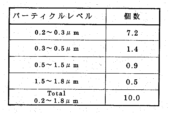
本発明(III)は、前記の洗浄方法を用いて洗浄された、ウェーハ表面上に付着するパーティクル数が少なく、表面粗れ(Ra)が少ない半導体ウェーハであり、ウェーハ表面上に付着するパーティクル数としては、0.2μm以上のパーティクルとして100個以下である。このパーティクル数はウェーハの大きさにより制限されるものではない。また、表面粗れ(Ra)はウェーハの種類によって異なり、シリコンウェーハの場合には0.2nm以下であり、ガリウム砒素ウェーハの場合には0.4nm以下である。
【0031】
次に、本発明(IV)の半導体ウェーハの製造方法について説明する。ここでは、シリコンウェーハの製造方法について説明するが、本発明(IV)はシリコンウェーハの製造方法に限定されるものではない。
本発明(IV)の半導体ウェーハの製造方法は、ウェーハ表面を磨くラップ工程、ウェーハ表面を鏡面研磨するポリッシュ工程及び洗浄工程を含むことを特徴とする。先ず、シリコン単結晶の引き上げが行われ、引き上げられたインゴットは、外周研削、オリエンテーションフラット加工を経て、ウェーハ状に切断される。作製されたウェーハは、次にベベリング(側面磨き)、ラップ(表面磨き)の工程を経て、ポリッシュ(鏡面研磨)工程に送られる。ウェーハの鏡面研磨は、ワックス(接着剤)でウェーハをガラスあるいはセラミック製のプレート(治具)に接着・固定した後、ウェーハ表面を研磨材と研磨布で研磨する。鏡面研磨終了後のウェーハは、プレートから剥がされ、ウェーハ上に付着したワックスやパーティクル、あるいは金属不純物等の汚染を除去するための洗浄工程へ送られる。この洗浄工程は、(1)前記の洗浄剤組成物を用いる洗浄工程と、(2)アンモニア及び過酸化水素を含有する洗浄剤を用いる洗浄工程、を含みウェーハの洗浄が終了した段階で、表面検査を行い、製品となる。
【0032】
【実施例】
以下に実施例及び比較例を用いて本発明をより詳細に説明するが、本発明はこれらの実施例に限定されるものではない。
(実施例1)ぬれ性
TMAH0.35質量%とパーフルオロカプリル酸100ppmを含有する洗浄剤水溶液のシリコンウェーハ、ガリウム砒素ウェーハに対する接触角を測定し、その結果を表1に示した。
【0033】
(比較例1)
TMAH0.35質量%を含有する洗浄剤水溶液のシリコンウェーハ、ガリウム砒素ウェーハに対する接触角を測定し、その結果を表1に示した。
【0034】
【表1】
【0035】
(実施例2)ワックス除去性
市販のワックス[商品名:アルファリキッドTR−100(インクテック社製)]を4インチガリウム砒素ウェーハ表面に1.7μmの膜厚で塗布し、これを80℃で5分間ベーキングし、試験用ウェーハを作製した。
試験用ウェーハを表2に示す洗浄剤組成物中に25℃で6分間浸漬し、その後、超純水で6分間リンスし、乾燥を行なった。処理後のウェーハ表面に集光燈をあて、肉眼にてワックス除去性を確認し、その結果を表2に示した。結果は、○−ワックスが完全に除去されている、△−ワックスが一部残っている、×−ワックスがウェーハ全面に残っている、の3段階で評価した。
【0036】
(比較例2、3)
実施例2と同じ方法で作製した試験用ウェーハを、表2に示す洗浄剤組成物中にそれぞれ浸漬した。その後、実施例2と同様に処理を行い、ワックス除去性を確認し、その結果を表2に示した。
【0037】
【表2】
【0038】
(実施例3)パーティクル除去性(1)(ガリウム砒素ウェーハ洗浄試験)
4インチガリウム砒素ウェーハ製造工程において、ラップ工程、エッチング工程を行った後のウェーハを、市販のワックス[商品名:アルファリキッドTR−100(インクテック社製)]でガラスプレート上に接着・固定し、ウェーハ表面を研磨剤と研磨布で鏡面研磨した。鏡面研磨終了後のウェーハをプレートから剥がし、これを試験用ウェーハとした。
【0039】
TMAH3.2質量%、ジエタノールアミン12.8質量%を含有する水溶液にパーフルオロカプリル酸を2000ppmとなるように添加し、この溶液を超純水で20倍に希釈して、ガリウム砒素ウェーハのパーティクル除去洗浄試験を行った。
洗浄試験は、試験用ウェーハを25℃で上記の希釈した洗浄液中に9分間浸漬し、次に25℃の超純水中においてリンス洗浄を6分間行った。その後、ウェーハの乾燥をIPA乾燥機を用いて1分間かけて行った。洗浄後、ウェーハ表面のパーティクルレベル(単位:個/ウェーハ、n=9)を測定し、その結果を表3に示した。
【0040】
(比較例4)
TMAH3.2質量%、ジエタノールアミン12.8質量%を含有する水溶液にポリオキシエチレンノニルフェニルエーテルを2000ppmとなるように添加し、この溶液を超純水で20倍に希釈し、実施例3と同様にしてガリウム砒素ウェーハの洗浄試験を行った。洗浄後、ウェーハ表面のパーティクルレベル(単位:個/ウェーハ、n=9)を測定し、その結果を表3に示した。
【0041】
【表3】
【0042】
(実施例4)パーティクル除去性(2)(シリコンウェーハ洗浄試験)
6インチシリコンウェーハ製造工程において、ラップ工程、エッチング工程を行った後のウェーハを、市販のワックス[商品名:アルファリキッドTR−120(インクテック社製)]でガラスプレート上に接着・固定し、ウェーハ表面を研磨剤と研磨布で鏡面研磨した。鏡面研磨終了後のウェーハをプレートから剥がし、これを試験用ウェーハとした。
【0043】
TMAH1.3質量%を含有する水溶液にパーフルオロカプリル酸を100ppmとなるように添加した溶液を超純水で22倍に希釈し、過酸化水素水(30質量%水溶液)を3質量%となるように添加して、この溶液をシリコンウェーハ表面のパーティクル除去洗浄試験に使用した。
洗浄試験は、先ず75℃まで加熱した上記の洗浄液中に試験用ウェーハを6分間浸漬し、次に25℃の超純水中でリンス洗浄を6分間行った。さらに、75℃で、アンモニアと過酸化水素を含有する洗浄液を用いた洗浄を6分間行い、次に25℃の超純水中でリンス洗浄を6分間行った。その後、ウェーハの乾燥をIPA乾燥機を用いて1分間かけて行った。洗浄後、ウェーハ表面のパーティクルレベル(単位:個/ウェーハ、n=25)を測定し、その結果を表4に示した。
【0044】
【表4】
【0045】
(実施例5)シリコンウェーハの食刻作用
6インチシリコンウェーハを表5に示した洗浄剤組成物中に60℃で5分間浸漬し、その後、超純水で6分間リンスし、乾燥を行なった。洗浄テスト後のウェーハ表面の粗らさを原子間力顕微鏡を用いて測定し、その結果をウェーハ表面粗れ(Ra)として表5に示した。
【0046】
(比較例6)
6インチシリコンウェーハを、TMAH0.13質量%を含有する洗浄剤を用いて実施例5と同様にして洗浄し、洗浄テスト後のウェーハ表面粗らさを原子間力顕微鏡を用いて測定し、その結果を表5に示した。
【0047】
【表5】
【0048】
(実施例6)ガリウム砒素ウェーハの食刻作用
4インチガリウム砒素ウェーハについて、25℃で同様に表6に示した洗浄剤組成物を用いて食刻作用試験を行い、試験後のウェーハ表面粗らさを測定し、その結果を表6に示した。
【0049】
【表6】
【0050】
【発明の効果】
本発明の洗浄剤組成物を用いれば、比較的単時間で半導体ウェーハあるいはウェーハ製造に使用されるガラス、セラミック製器具等の表面上の汚染物質を速やかに除去することができる。特に本発明の洗浄剤組成物はワックスの洗浄力が高く、食刻が十分に制御され、洗浄処理後の表面状態も極めて良好である。[0001]
BACKGROUND OF THE INVENTION
The present invention relates to a cleaning composition, a cleaning method, a semiconductor wafer, and a semiconductor wafer manufacturing method used to remove surface contamination of semiconductor wafers or precision processed glass used in wafer manufacturing, ceramic instruments, etc. Regarding the method.
[0002]
[Prior art]
Semiconductor devices such as transistors, diodes, ICs, LSIs, and rectifiers are manufactured by adding steps such as vapor phase growth, oxide film formation, impurity diffusion, and electrode metal film deposition to silicon wafers and compound semiconductor wafers.
Since the semiconductor device is significantly affected by the electrical characteristics due to the impurities, the surface of the semiconductor wafer is sufficiently cleaned before each step to remove contamination by the impurities. As an industrial technique, many methods using a treatment liquid mainly composed of an organic alkali or a treatment liquid obtained by adding a complexing agent, a surfactant, hydrogen peroxide or the like to an organic alkali have been proposed.
[0003]
In JP-A-50-147287, among tetraalkylammonium hydroxides, for example, tetramethylammonium hydroxide (hereinafter “TMAH”) is also referred to. ) Etc. are described as being effective for degreasing, removal of contamination by inorganic substances, and removal of extremely thin oxide films. However, (1) The wettability to the surface to be processed is poor, so the cleaning power is not sufficient. (2) It has an etching dependency on the orientation of the silicon crystal. On the other hand, the (111) plane shows resistance to the etching action, and the (100) mirror surface wafer is roughened by the etching).
Japanese Patent Application Laid-Open No. 50-158281 describes a solution in which a complexing agent is added to TMAH. In this case, the cleaning power is improved as compared with the case of TMAH alone, but the wetness to the surface to be processed is poor and the cleaning power is still insufficient.
[0004]
As for the etching of the silicon crystal, it is possible to suppress the etching of the silicon crystal just by adding a surfactant to the alkaline aqueous solution. It is not that a sufficient effect is obtained under all conditions. In some cases, hydrogen peroxide is used in addition to alkali and surfactant. For example, Japanese Patent Application Laid-Open No. 63-274149 describes that etching is sufficiently controlled when hydrogen peroxide is used in addition to a tetraalkylammonium hydroxide and a nonionic surfactant. . However, there remains a problem that the particle removal performance is not sufficient.
[0005]
In addition, as described in Japanese Patent No. 2579401, a case in which alkanolamine is added to a tetraalkylammonium hydroxide and a nonionic surfactant is also known. Although the detergency is improved by adding alkanolamine, the problem that the particle removal performance is not sufficient in this case also remains.
In recent years, with the high integration of semiconductors, the need to remove impurities is increasing, and a new cleaning solution with high impurity removal effect and re-adsorption prevention effect of desorbed impurities and well-controlled etching. It has been demanded.
[0006]
[Problems to be solved by the invention]
The present invention has been made under such a background, and is excellent in cleaning against surface contamination of various kinds of precision-processed glass and ceramic instruments used for manufacturing semiconductor wafers or semiconductor wafers. It is an object of the present invention to provide a cleaning composition having power, a wafer cleaning method, a semiconductor wafer, and a semiconductor wafer manufacturing method.
[0007]
[Means for Solving the Problems]
As a result of intensive studies to solve the above problems, the present inventors have found that a specific fluorine-based anionic surfactant and a quaternary ammonium hydroxideOr a specific fluorine-based anionic surfactant, a quaternary ammonium hydroxide, andThe present inventors have found that the above-mentioned problems can be solved by using a detergent composition containing alkanolamine, and have completed the present invention.
[0008]
That is, the present invention (I) includes 0.0001 to 5% by mass of a fluorine-based anionic surfactant and 0.001 to 30% by mass of a quaternary ammonium hydroxide.A cleaning composition characterized by containing 0.001 to 5% by mass of a fluorine-based anionic surfactant, 0.001 to 30% by mass of a quaternary ammonium hydroxide, andA cleaning composition containing 0.01 to 20% by mass of alkanolamine. In the present invention (I), the fluorine-based anionic surfactant is represented by the following general formula (1).
R1COOM (1)
(Wherein R1Is a linear or branched alkyl or alkenyl group having 2 to 20 carbon atoms in which part or all of the hydrogen atoms are substituted with fluorine atoms, and M is a hydrogen atom, an alkali metal atom, or an ammonium group Represents an alkylammonium group or an alkanolammonium group. ) Carboxylic acid represented by the following formula (2)
R2SO3M (2)
(Wherein R2Is a linear or branched alkyl group or alkenyl group having 2 to 20 carbon atoms in which part or all of the hydrogen atoms are substituted with fluorine atoms, and M represents the same meaning as described above. ) And at least one compound selected from the group consisting of salts thereof, and the fluoroanionic surfactant is perfluorocaprylic acid, perfluorocapric acid, perfluorooctanesulfonic acid. And at least one compound selected from the group consisting of the salts thereof is a preferred embodiment.
[0009]
Further, the quaternary ammonium hydroxide is represented by the following general formula (3)
[Chemical 3]
[0010]
Further, the alkanolamine is represented by the following general formula (4)
[Formula 4]
[0011]
Moreover, in this invention (I), it contains 0.0001-5 mass% of nonionic surfactant, Furthermore, nonionic surfactant is following General formula (5).
R10-O- (R11-O)p-H (5)
(Wherein R10Is an alkyl group having 6 to 20 carbon atoms, R11Represents an alkylene group having 2 to 4 carbon atoms, and p represents an integer of 3 to 20. ) Polyoxyalkylene alkyl ether type represented by the following general formula (6)
R12-C6H4-O- (R13-O)q-H (6)
(Wherein R12Is an alkyl group having 6 to 20 carbon atoms, R13Represents an alkylene group having 2 to 4 carbon atoms, and q represents an integer of 3 to 20. ) And the following general formula (7)
R14-COO- (R15-O)r-H (7)
(Wherein R14Is an alkyl group having 9 to 16 carbon atoms, R15Represents an alkylene group having 2 to 4 carbon atoms, and r represents an integer of 6 to 16. And at least one compound selected from the group consisting of the polyoxyalkylene alkyl ester type represented by formula (II) is a preferred embodiment. Containing mass% is also a preferred embodiment.
[0012]
The present invention (II) includes (1) a cleaning step using the above-described cleaning composition, and (2) a cleaning step using a cleaning agent containing ammonia and hydrogen peroxide. In the preferred embodiment, the cleaning step (1) performs degreasing and particle removal on the semiconductor wafer surface, and the cleaning step (2) performs particle removal on the semiconductor wafer surface.
[0013]
The present invention (III) is a semiconductor wafer having a surface cleaned by the above-described cleaning method, the number of adhered particles of 0.2 μm or more on the semiconductor wafer surface is 100 or less, the semiconductor wafer is a silicon wafer, A gallium phosphide wafer, a gallium arsenide wafer or an indium phosphide wafer is a preferred embodiment, the semiconductor wafer is a silicon wafer, the surface roughness (Ra) is 0.2 nm or less, and the semiconductor wafer is gallium. An arsenic wafer having a surface roughness (Ra) of 0.4 nm or less is also a preferred embodiment.
[0014]
The present invention (IV) includes (1) a lapping process for polishing the wafer surface, (2) a polishing process for mirror polishing the wafer surface, and (3) a cleaning process using the above-described cleaning composition, and ammonia and hydrogen peroxide. And a cleaning step using a cleaning agent.
[0015]
DETAILED DESCRIPTION OF THE INVENTION
The present invention will be described in detail below.
First, the cleaning composition of the present invention (I) will be described.
The cleaning composition of the present invention comprises a fluorine-based anionic surfactant and a quaternary ammonium hydroxide.It is characterized by containing. The cleaning composition of the present invention is characterized by containing a fluorine-based anionic surfactant, a quaternary ammonium hydroxide and an alkanolamine.
As a fluorine-type anionic surfactant, following General formula (1)
R1COOM (1)
(Wherein R1And M represent the same meaning as described above. ) Carboxylic acid represented by the following formula (2)
R2SO3M (2)
(Wherein R2And M represent the same meaning as described above. And a fluorinated anionic surfactant which is at least one compound selected from the group consisting of sulfonic acids represented by the following formula:
[0016]
Preferably, R of the carboxylic acid represented by the general formula (1)1Is a linear or branched perfluoroalkyl group having 6 to 16 carbon atoms, a hydrofluoroalkyl group, a perfluoroalkenyl group, a carboxylic acid that is a hydrofluoroalkenyl group, a salt thereof, the general formula (2) R of sulfonic acid represented by2Is at least selected from the group consisting of linear or branched perfluoroalkyl groups having 6 to 12 carbon atoms, hydrofluoroalkyl groups, perfluoroalkenyl groups, sulfonic acids that are hydrofluoroalkenyl groups, and salts thereof. One kind of compound.
[0017]
Specifically, perfluoroheptanoic acid (C6F13COOH), perfluorocaprylic acid (C7F15COOH), perfluorononanoic acid (C8F17COOH), 5,5,6,6,7,7,8,8,9,9,9-undecafluorononanoic acid (C5F11(CH2)3COOH), perfluorocapric acid (C9F19COOH), perfluorododecanoic acid (C11F23COOH), 6, 6, 7, 7, 8, 8, 9, 9, 10, 10, 11, 11, 12, 12, 12-pentadecafluoro-4-dodecenoic acid (CF3(CF2)6CH = CH (CH2)2COOH), perfluorotetradecanoic acid (C13F27COOH), 12-trifluoromethyl-12,13,13,14,14,15,15,16,16,16-decafluorohexadecanoic acid (CF3(CF2)3CF (CF3) (CH2)10COOH), perfluorooctane sulfonic acid (C8F17SO3H), etc. and their ammonium salts, tetramethylammonium salts, and the like. More preferred are perfluorocaprylic acid, perfluorocapric acid, perfluorooctanesulfonic acid and salts thereof. Moreover, these compounds may be used independently and can also be used combining two or more types by arbitrary ratios.
[0018]
In the cleaning composition of the present invention, this fluorine-based anionic surfactant is an essential component, and is contained in an amount of 0.0001 to 5% by weight, preferably 0.0001 to 1% by weight, more preferably the entire cleaning agent. Is preferably contained in the range of 0.0001 to 0.5% by mass. When the content exceeds 5% by mass, problems of foaming and rinsing occur, which is not preferable. On the other hand, when the content is less than 0.0001% by mass, the effect of improving the detergency cannot be exhibited sufficiently.
[0019]
The quaternary ammonium hydroxide has the following general formula (3)
[Chemical formula 5]
[0020]
Moreover, as alkanolamine, following General formula (4)
[Chemical 6]
[0021]
The detergent composition of the present invention comprises a detergent containing two components of a fluorine-based anionic surfactant and a quaternary ammonium hydroxide, orBy containing three components of fluorinated anionic surfactant and quaternary ammonium hydroxide plus alkanolamineIt can be used as a cleaning agent having improved cleaning properties and life. When alkanolamine is used, it can be added in an amount of 0.01 to 20% by mass, preferably 0.1 to 10% by mass, and more preferably 0.1 to 5% by mass, based on the entire cleaning agent. When the concentration is higher than 20% by mass, there arises a problem that the cleaning performance is lowered, and it is not preferable economically.
[0022]
In addition to the fluorine-based anionic surfactant, quaternary ammonium hydroxide and alkanolamine, the cleaning composition of the present invention contains a nonionic surfactant for the purpose of suppressing etching on the wafer surface. Can be added. As the nonionic surfactant, the following general formula (5)
R10-O- (R11-O)p-H (5)
(Wherein R10, R11And p represent the same meaning as described above. ) Polyoxyalkylene alkyl ether type represented by the following general formula (6)
R12-C6H4-O- (R13-O)q-H (6)
(Wherein R12, R13And q represent the same meaning as described above. And a polyoxyalkylene aryl ether type represented by the following general formula (7):
R14-COO- (R15-O)r-H (7)
(Wherein R14, R15And r represent the same meaning as described above. And at least one compound selected from the group consisting of polyoxyalkylene alkyl ester types represented by
[0023]
The alkylene group of the nonionic surfactant is -CH2CH2-, -CH2CH2CH2-Is preferable, and -CH is particularly preferable.2CH2-. Specific examples of the polyoxyalkylene alkyl ether type include polyoxyethylene decanyl ether, polyoxyethylene undecanyl ether, polyoxyethylene dodecanyl ether, and polyoxyethylene tetradecanyl ether. In the polyoxyalkylene aryl ether type, polyoxyethylene nonyl phenyl ether, polyoxyethylene octyl phenyl ether, polyoxyethylene dodecyl phenyl ether and the like can be mentioned. In the polyoxyalkylene alkyl ester type, polyoxyethylene Examples include oleic acid esters. However, the nonionic surfactant is not limited to these.
This nonionic surfactant can be added in the range of 0.0001 to 5% by mass, preferably 0.0001 to 1% by mass, and more preferably 0.0001 to 0.5% by mass of the whole cleaning agent. . If it exceeds 5% by mass, foaming and rinsing problems occur, which is not preferable.
[0024]
Furthermore, hydrogen peroxide can be added to the cleaning composition of the present invention. In silicon wafer cleaning, wafer etching can be suppressed by simply adding a surfactant to the alkali, but the effect is greatly affected by the type of surfactant, alkali concentration, temperature, etc. However, it does not mean that a sufficient effect can be obtained. By using hydrogen peroxide, the etching is appropriately controlled even at high temperatures, and the use range of the cleaning composition of the present invention can be expanded.
When hydrogen peroxide is added, it can be added in the range of 0.01 to 20% by mass, preferably 0.05 to 10% by mass, based on the whole cleaning agent. When the concentration of hydrogen peroxide is higher than 20% by mass, the cleaning power itself is not particularly affected, but the amount of decomposition of hydrogen peroxide increases, which is uneconomical.
[0025]
The components constituting the cleaning agent of the present invention are a fluorine-based anionic surfactant and a quaternary ammonium hydroxide.A fluorine-based anionic surfactant, a quaternary ammonium hydroxide, andAlkanolamine is the basic component. By using a cleaning agent that is a combination of these basic components according to the usage conditions, it is possible to efficiently remove contamination on the wafer surface and prevent reattachment of contaminants. Depending on the use conditions, a nonionic surfactant or hydrogen peroxide is added in a timely manner for the purpose of suppressing etching by alkali on the wafer surface. For example, in the cleaning of a silicon wafer, when a cleaning agent is used at a high temperature of, for example, 60 to 80 ° C., it is preferable to add hydrogen peroxide because the etching of the wafer by alkali becomes large. On the other hand, when using the cleaning agent of the present invention at room temperature, a nonionic surfactant may be added instead of hydrogen peroxide, or both hydrogen peroxide and a nonionic surfactant may be added. Good. Etching of wafers varies depending on the type of wafer. For example, in the cleaning of gallium arsenide wafers, the etching action on the wafer surface by alkali is extremely small, so depending on the use conditions, nonionic surfactants and hydrogen peroxide It is not necessary to add. Moreover, the cleaning composition of the present invention can be suitably used for cleaning under moderate heating and cleaning using ultrasonic waves, as well as exhibiting an excellent cleaning effect even at room temperature. Surface contamination of precision processed glass, ceramic appliances, etc. used in wafer manufacture can be removed.
[0026]
Next, a method for cleaning a semiconductor wafer according to the present invention (II) will be described.
The semiconductor wafer cleaning method of the present invention includes (1) a cleaning step using the above-described cleaning composition, and (2) a cleaning step using a cleaning agent containing ammonia and hydrogen peroxide. . The cleaning step (1) is mainly for degreasing and removing particles on the surface of the semiconductor wafer, and the cleaning step (2) is mainly for removing particles on the surface of the semiconductor wafer.
[0027]
A typical example of the process of degreasing the semiconductor wafer surface and removing particles is wax cleaning after mirror polishing of the wafer. Since mirror polishing of semiconductor wafers is performed by bonding and fixing the wafer to a plate (jig) with wax, when the wafer is peeled off from the plate after polishing, a large amount of wax used as an adhesive adheres to the wafer. And remain. The cleaning composition of the present invention is particularly effective for cleaning for removing wax and particles adhering to the wafer.
[0028]
The cleaning composition of the present invention has both a wax removing effect and a particle removing effect even when used alone, but can also be used in combination with other cleaning agents. Here, a cleaning method for performing wax removal cleaning and particle removal cleaning of a semiconductor wafer using the cleaning composition of the present invention and further performing particle removal cleaning using a cleaning agent of another composition will be described. First, for example, cleaning with wax and particles is performed using the cleaning agent of the present invention in which perfluorocaprylic acid is added to a tetramethylammonium hydroxide aqueous solution. Hydrogen peroxide can be added to this cleaning agent as required. Next, particle removal cleaning is performed using a cleaning agent containing ammonia and hydrogen peroxide. Each washing step may be performed a plurality of times, for example, a rinsing step using water may be performed, and after the entire washing step is completed, drying is performed using an organic solvent such as isopropyl alcohol. In this way, not only the wax is removed from the semiconductor wafer after cleaning, but also the particle level can be reduced as compared with the case where the conventional cleaning liquid is used.
[0029]
In the above two cleaning steps, the cleaning temperature, the cleaning conditions, etc. are not particularly limited, and appropriate conditions can be appropriately selected depending on the wafer to be cleaned. Examples of semiconductor wafers that can be cleaned using the cleaning method of the present invention include single-element semiconductors such as silicon and germanium, or compound semiconductors such as gallium phosphide, gallium arsenide, and indium phosphide.
[0030]
The present invention (III) is a semiconductor wafer that has been cleaned using the above-described cleaning method and has a small number of particles adhering to the wafer surface and a small surface roughness (Ra), and the number of particles adhering to the wafer surface. The number is 100 or less as particles having a size of 0.2 μm or more. The number of particles is not limited by the size of the wafer. The surface roughness (Ra) varies depending on the type of wafer, and is 0.2 nm or less for a silicon wafer and 0.4 nm or less for a gallium arsenide wafer.
[0031]
Next, a method for manufacturing a semiconductor wafer according to the present invention (IV) will be described. Here, although the manufacturing method of a silicon wafer is demonstrated, this invention (IV) is not limited to the manufacturing method of a silicon wafer.
The method for producing a semiconductor wafer according to the present invention (IV) includes a lapping step for polishing the wafer surface, a polishing step for mirror polishing the wafer surface, and a cleaning step. First, the silicon single crystal is pulled up, and the pulled ingot is cut into a wafer through peripheral grinding and orientation flat processing. The produced wafer is then sent to a polishing (mirror polishing) step through steps of beveling (side polishing) and lapping (surface polishing). In mirror polishing of a wafer, a wafer is bonded and fixed to a glass or ceramic plate (jig) with wax (adhesive), and then the wafer surface is polished with an abrasive and a polishing cloth. The wafer after mirror polishing is peeled off from the plate and sent to a cleaning process for removing contamination such as wax, particles or metal impurities adhering to the wafer. This cleaning process includes (1) a cleaning process using the above-described cleaning composition, and (2) a cleaning process using a cleaning agent containing ammonia and hydrogen peroxide. Inspects and becomes a product.
[0032]
【Example】
Hereinafter, the present invention will be described in more detail with reference to Examples and Comparative Examples, but the present invention is not limited to these Examples.
(Example 1) Wettability
The contact angle of a cleaning agent aqueous solution containing 0.35% by mass of TMAH and 100 ppm of perfluorocaprylic acid to a silicon wafer and a gallium arsenide wafer was measured, and the results are shown in Table 1.
[0033]
(Comparative Example 1)
The contact angle of the cleaning agent aqueous solution containing 0.35% by mass of TMAH with respect to the silicon wafer and the gallium arsenide wafer was measured, and the results are shown in Table 1.
[0034]
[Table 1]
[0035]
(Example 2) Wax removability
A commercially available wax [trade name: Alpha Liquid TR-100 (manufactured by Inktec)] was applied to the surface of a 4-inch gallium arsenide wafer with a film thickness of 1.7 μm, and this was baked at 80 ° C. for 5 minutes to test wafers. Was made.
The test wafer was dipped in the cleaning composition shown in Table 2 at 25 ° C. for 6 minutes, then rinsed with ultrapure water for 6 minutes and dried. The wafer surface after the treatment was applied with a condensing rod, and the wax removability was confirmed with the naked eye. The results are shown in Table 2. The results were evaluated in three stages: o-wax completely removed, Δ-wax partially left, and x-wax left on the entire wafer surface.
[0036]
(Comparative Examples 2 and 3)
Test wafers produced by the same method as in Example 2 were each immersed in the cleaning composition shown in Table 2. Thereafter, the treatment was performed in the same manner as in Example 2 to confirm the wax removability, and the results are shown in Table 2.
[0037]
[Table 2]
[0038]
Example 3 Particle Removability (1) (Gallium Arsenide Wafer Cleaning Test)
In the 4-inch gallium arsenide wafer manufacturing process, the wafer after the lapping process and the etching process are bonded and fixed on a glass plate with a commercially available wax [trade name: Alpha Liquid TR-100 (manufactured by Inktec Co., Ltd.)]. The wafer surface was mirror-polished with an abrasive and a polishing cloth. The wafer after mirror polishing was peeled off from the plate and used as a test wafer.
[0039]
Perfluorocaprylic acid was added to an aqueous solution containing 3.2% by mass of TMAH and 12.8% by mass of diethanolamine so that the concentration was 2000 ppm, and this solution was diluted 20 times with ultrapure water to remove particles from the gallium arsenide wafer. A cleaning test was performed.
In the cleaning test, the test wafer was immersed in the diluted cleaning solution at 25 ° C. for 9 minutes, and then rinsed in ultrapure water at 25 ° C. for 6 minutes. Thereafter, the wafer was dried using an IPA dryer for 1 minute. After cleaning, the particle level (unit: piece / wafer, n = 9) on the wafer surface was measured, and the results are shown in Table 3.
[0040]
(Comparative Example 4)
Polyoxyethylene nonylphenyl ether was added to an aqueous solution containing 3.2% by mass of TMAH and 12.8% by mass of diethanolamine so as to be 2000 ppm, and this solution was diluted 20 times with ultrapure water, and the same as in Example 3. Then, a cleaning test of the gallium arsenide wafer was performed. After cleaning, the particle level (unit: piece / wafer, n = 9) on the wafer surface was measured, and the results are shown in Table 3.
[0041]
[Table 3]
[0042]
(Example 4) Particle removability (2) (silicon wafer cleaning test)
In the 6-inch silicon wafer manufacturing process, the wafer after the lapping process and the etching process are bonded and fixed on a glass plate with a commercially available wax [trade name: Alpha Liquid TR-120 (manufactured by Inktec)], The wafer surface was mirror-polished with an abrasive and a polishing cloth. The wafer after mirror polishing was peeled off from the plate and used as a test wafer.
[0043]
A solution obtained by adding perfluorocaprylic acid to an aqueous solution containing 1.3% by mass of TMAH so as to be 100 ppm is diluted 22 times with ultrapure water, and hydrogen peroxide solution (30% by mass aqueous solution) is 3% by mass. This solution was used for a particle removal cleaning test on the surface of a silicon wafer.
In the cleaning test, the test wafer was first immersed in the cleaning solution heated to 75 ° C. for 6 minutes, and then rinsed in ultrapure water at 25 ° C. for 6 minutes. Further, cleaning with a cleaning solution containing ammonia and hydrogen peroxide was performed at 75 ° C. for 6 minutes, and then rinse cleaning was performed in ultrapure water at 25 ° C. for 6 minutes. Thereafter, the wafer was dried using an IPA dryer for 1 minute. After cleaning, the particle level (unit: piece / wafer, n = 25) on the wafer surface was measured, and the results are shown in Table 4.
[0044]
[Table 4]
[0045]
(Example 5) Etching action of silicon wafer
A 6-inch silicon wafer was immersed in the cleaning composition shown in Table 5 at 60 ° C. for 5 minutes, then rinsed with ultrapure water for 6 minutes and dried. The roughness of the wafer surface after the cleaning test was measured using an atomic force microscope, and the result is shown in Table 5 as the wafer surface roughness (Ra).
[0046]
(Comparative Example 6)
A 6-inch silicon wafer was cleaned in the same manner as in Example 5 using a cleaning agent containing 0.13% by mass of TMAH, and the wafer surface roughness after the cleaning test was measured using an atomic force microscope. The results are shown in Table 5.
[0047]
[Table 5]
[0048]
(Example 6) Etching of gallium arsenide wafer
A 4-inch gallium arsenide wafer was similarly etched at 25 ° C. using the cleaning composition shown in Table 6, and the wafer surface roughness after the test was measured. The results are shown in Table 6. It was.
[0049]
[Table 6]
[0050]
【The invention's effect】
By using the cleaning composition of the present invention, it is possible to quickly remove contaminants on the surface of a semiconductor wafer or a glass or ceramic instrument used for manufacturing a wafer in a relatively short time. In particular, the cleaning composition of the present invention has a high detergency of wax, etching is sufficiently controlled, and the surface condition after the cleaning treatment is extremely good.
Claims (20)
R1COOM (1)
(式中、R1は水素原子の一部または全部がフッ素原子で置換された、炭素数が2〜20の直鎖状または分岐鎖状のアルキル基またはアルケニル基であり、Mは水素原子、アルカリ金属原子、アンモニウム基、アルキルアンモニウム基またはアルカノールアンモニウム基を表す。)で表されるカルボン酸、その塩、下記一般式(2)
R2SO3M (2)
(式中、R2は水素原子の一部または全部がフッ素原子で置換された、炭素数が2〜20の直鎖状または分岐鎖状のアルキル基またはアルケニル基であり、Mは前記と同様の意味を表す。)で表されるスルホン酸及びその塩からなる群から選ばれる少なくとも1種の化合物である請求項1または2に記載の洗浄剤組成物。Fluorine anionic surfactant is represented by the following general formula (1)
R 1 COOM (1)
(Wherein R 1 is a linear or branched alkyl or alkenyl group having 2 to 20 carbon atoms in which part or all of the hydrogen atoms are substituted with fluorine atoms, M is a hydrogen atom, Represents an alkali metal atom, an ammonium group, an alkylammonium group or an alkanolammonium group.), A salt thereof, the following general formula (2)
R 2 SO 3 M (2)
(Wherein R 2 is a linear or branched alkyl group or alkenyl group having 2 to 20 carbon atoms in which part or all of the hydrogen atoms are substituted with fluorine atoms, and M is the same as defined above. detergent composition according to claim 1 or 2 is at least one compound selected from the group consisting meaning from sulfonic acid and a salt thereof represents.) of.
R10−O−(R11−O)p−H (5)
(式中、R10は炭素数が6〜20のアルキル基、R11は炭素数が2〜4のアルキレン基、pは3〜20の整数を表す。)で表されるポリオキシアルキレンアルキルエーテル型、下記一般式(6)
R12−C6H4−O−(R13−O)q−H (6)
(式中、R12は炭素数が6〜20のアルキル基、R13は炭素数が2〜4のアルキレン基、qは3〜20の整数を表す。)で表されるポリオキシアルキレンアリールエーテル型及び下記一般式(7)
R14−COO−(R15−O)r−H (7)
(式中、R14は炭素数が9〜16のアルキル基、R15は炭素数が2〜4のアルキレン基、rは6〜16の整数を表す。)で表されるポリオキシアルキレンアルキルエステル型からなる群から選ばれる少なくとも1種の化合物である請求項1〜9のいずれかに記載の洗浄剤組成物。The nonionic surfactant is represented by the following general formula (5)
R 10 —O— (R 11 —O) p —H (5)
(Wherein R 10 is an alkyl group having 6 to 20 carbon atoms, R 11 is an alkylene group having 2 to 4 carbon atoms, and p is an integer of 3 to 20). Type, following general formula (6)
R 12 -C 6 H 4 -O- ( R 13 -O) q -H (6)
(Wherein R 12 represents an alkyl group having 6 to 20 carbon atoms, R 13 represents an alkylene group having 2 to 4 carbon atoms, and q represents an integer of 3 to 20). Type and following general formula (7)
R 14 —COO— (R 15 —O) r —H (7)
(Wherein R 14 represents an alkyl group having 9 to 16 carbon atoms, R 15 represents an alkylene group having 2 to 4 carbon atoms, and r represents an integer of 6 to 16). The cleaning composition according to any one of claims 1 to 9 , which is at least one compound selected from the group consisting of molds.
(1)請求項1〜11のいずれかに記載の洗浄剤組成物を用いる洗浄工程
(2)アンモニア及び過酸化水素を含有する洗浄剤を用いる洗浄工程A semiconductor wafer cleaning method comprising the following two cleaning steps.
(1) Cleaning step using the cleaning composition according to any one of claims 1 to 11 (2) Cleaning step using a cleaning agent containing ammonia and hydrogen peroxide
(1)ウェーハ表面を磨くラップ工程
(2)ウェーハ表面を鏡面研磨するポリッシュ工程
(3)請求項1〜11のいずれかに記載の洗浄剤組成物を用いる洗浄工程とアンモニア及び過酸化水素を含有する洗浄剤を用いる洗浄工程The manufacturing method of the semiconductor wafer characterized by including the following three processes.
(1) A lapping step for polishing the wafer surface (2) A polishing step for mirror polishing the wafer surface (3) A cleaning step using the cleaning composition according to any one of claims 1 to 11 , containing ammonia and hydrogen peroxide Cleaning process using cleaning agent
Priority Applications (5)
| Application Number | Priority Date | Filing Date | Title |
|---|---|---|---|
| JP2000250540A JP3624809B2 (en) | 2000-02-29 | 2000-08-22 | Cleaning composition, cleaning method and use thereof |
| TW090104573A TW593672B (en) | 2000-02-29 | 2001-02-27 | Cleaning agent composition, method for cleaning and use thereof |
| US09/794,620 US6417147B2 (en) | 2000-02-29 | 2001-02-28 | Cleaning agent composition, method for cleaning and use thereof |
| KR1020010010587A KR100789776B1 (en) | 2000-02-29 | 2001-02-28 | Cleaning agent composition, method for cleaning and use thereof |
| US10/112,855 US20020155964A1 (en) | 2000-02-29 | 2002-04-02 | Cleaning agent composition, method for cleaning and use thereof |
Applications Claiming Priority (3)
| Application Number | Priority Date | Filing Date | Title |
|---|---|---|---|
| JP2000-54670 | 2000-02-29 | ||
| JP2000054670 | 2000-02-29 | ||
| JP2000250540A JP3624809B2 (en) | 2000-02-29 | 2000-08-22 | Cleaning composition, cleaning method and use thereof |
Publications (2)
| Publication Number | Publication Date |
|---|---|
| JP2001316691A JP2001316691A (en) | 2001-11-16 |
| JP3624809B2 true JP3624809B2 (en) | 2005-03-02 |
Family
ID=26586445
Family Applications (1)
| Application Number | Title | Priority Date | Filing Date |
|---|---|---|---|
| JP2000250540A Expired - Fee Related JP3624809B2 (en) | 2000-02-29 | 2000-08-22 | Cleaning composition, cleaning method and use thereof |
Country Status (3)
| Country | Link |
|---|---|
| JP (1) | JP3624809B2 (en) |
| KR (1) | KR100789776B1 (en) |
| TW (1) | TW593672B (en) |
Families Citing this family (15)
| Publication number | Priority date | Publication date | Assignee | Title |
|---|---|---|---|---|
| TWI314950B (en) | 2001-10-31 | 2009-09-21 | Hitachi Chemical Co Ltd | Polishing slurry and polishing method |
| JP4850167B2 (en) * | 2001-10-31 | 2012-01-11 | 日立化成工業株式会社 | Polishing liquid and polishing method |
| JP4304988B2 (en) * | 2002-01-28 | 2009-07-29 | 三菱化学株式会社 | Semiconductor device substrate cleaning method |
| US7176041B2 (en) | 2003-07-01 | 2007-02-13 | Samsung Electronics Co., Ltd. | PAA-based etchant, methods of using same, and resultant structures |
| US20060003910A1 (en) | 2004-06-15 | 2006-01-05 | Hsu Jiun Y | Composition and method comprising same for removing residue from a substrate |
| CN102064090B (en) * | 2010-10-15 | 2013-01-09 | 北京通美晶体技术有限公司 | Method for cleaning compound semiconductor chip |
| KR101448026B1 (en) * | 2013-08-26 | 2014-10-08 | 주식회사 원익큐엔씨 | Method for bonding silicon-containing materials using orgenic solvent |
| KR101448025B1 (en) * | 2013-08-26 | 2014-10-08 | 주식회사 원익큐엔씨 | Method for bonding silicon-containing materials |
| EP3258481A4 (en) * | 2015-02-09 | 2018-09-19 | Sumitomo Electric Industries, Ltd. | Indium phosphorus substrate, indium phosphorus substrate inspection method, and indium phosphorus substrate manufacturing method |
| CN108816870B (en) * | 2018-04-08 | 2021-05-25 | 苏州珮凯科技有限公司 | Regeneration method of ceramic annular part of WxZ process in thin film manufacturing process of semiconductor 8-inch wafer |
| CN108753478A (en) * | 2018-06-19 | 2018-11-06 | 成都青洋电子材料有限公司 | A kind of single crystal silicon semiconductor cleaning agent and its cleaning method |
| CN109370795B (en) * | 2018-12-12 | 2020-10-02 | 太仓宝霓实业有限公司 | Oil removing agent for continuously processing polyester/ammonia and nylon/ammonia blended knitted fabric and preparation method thereof |
| US20230129238A1 (en) * | 2020-03-31 | 2023-04-27 | Nissan Chemical Corporation | Cleaning agent composition and method for producing processed semiconductor substrate |
| KR20250019013A (en) * | 2022-05-27 | 2025-02-07 | 카오카부시키가이샤 | Detergent composition for adhesives |
| CN115216370A (en) * | 2022-07-07 | 2022-10-21 | 呼和浩特市欧通能源科技有限公司 | Degumming liquid for removing adhesive in silicon crystal clamping piece and using method thereof |
Family Cites Families (4)
| Publication number | Priority date | Publication date | Assignee | Title |
|---|---|---|---|---|
| KR920013664A (en) * | 1990-12-07 | 1992-07-29 | 김광호 | Individual chip separation method of semiconductor wafer |
| JPH08195369A (en) * | 1995-01-13 | 1996-07-30 | Daikin Ind Ltd | Substrate cleaning method |
| JP3569031B2 (en) * | 1995-05-22 | 2004-09-22 | 株式会社ネオス | Practice golf ball cleaner and cleaning method |
| JP2001040389A (en) * | 1999-07-26 | 2001-02-13 | Daikin Ind Ltd | Wafer cleaning liquid |
-
2000
- 2000-08-22 JP JP2000250540A patent/JP3624809B2/en not_active Expired - Fee Related
-
2001
- 2001-02-27 TW TW090104573A patent/TW593672B/en not_active IP Right Cessation
- 2001-02-28 KR KR1020010010587A patent/KR100789776B1/en not_active Expired - Fee Related
Also Published As
| Publication number | Publication date |
|---|---|
| TW593672B (en) | 2004-06-21 |
| KR100789776B1 (en) | 2007-12-28 |
| JP2001316691A (en) | 2001-11-16 |
| KR20010085738A (en) | 2001-09-07 |
Similar Documents
| Publication | Publication Date | Title |
|---|---|---|
| US6417147B2 (en) | Cleaning agent composition, method for cleaning and use thereof | |
| JP4350364B2 (en) | Cleaning composition, semiconductor wafer cleaning method and manufacturing method | |
| JP5749457B2 (en) | Formulations and methods for post-CMP cleaning | |
| JP4304988B2 (en) | Semiconductor device substrate cleaning method | |
| KR100913557B1 (en) | Cleaning solution and cleaning method for substrate for semiconductor device | |
| KR100748410B1 (en) | Substrate surface cleaning liquid mediums and cleaning method | |
| KR101166002B1 (en) | Substrate cleaning liquid for semiconductor device and cleaning method | |
| JP4931953B2 (en) | Semiconductor substrate cleaning liquid composition | |
| US6896744B2 (en) | Method for cleaning a surface of a substrate | |
| KR101520917B1 (en) | Texturing and cleaning agent for the surface treatment of wafers and use thereof | |
| JP3624809B2 (en) | Cleaning composition, cleaning method and use thereof | |
| TWI565797B (en) | Cleaning fluid composition for electronic components | |
| KR20010024201A (en) | Aqueous rinsing composition | |
| JP4736445B2 (en) | Substrate cleaning solution for semiconductor device and cleaning method | |
| JPWO2009072529A1 (en) | Semiconductor device substrate cleaning method and cleaning liquid | |
| JP2003068696A (en) | Substrate surface cleaning method | |
| JP2003109930A (en) | Cleaning solution and method of cleaning board of semiconductor device | |
| JP2003088817A (en) | Substrate surface cleaning method | |
| JP2001217215A (en) | Composition and method for treating surface of semiconductor substrate | |
| JP4718762B2 (en) | Semiconductor substrate cleaning liquid composition |
Legal Events
| Date | Code | Title | Description |
|---|---|---|---|
| A977 | Report on retrieval |
Free format text: JAPANESE INTERMEDIATE CODE: A971007 Effective date: 20040628 |
|
| A131 | Notification of reasons for refusal |
Free format text: JAPANESE INTERMEDIATE CODE: A131 Effective date: 20040713 |
|
| A521 | Request for written amendment filed |
Free format text: JAPANESE INTERMEDIATE CODE: A523 Effective date: 20040910 |
|
| TRDD | Decision of grant or rejection written | ||
| A01 | Written decision to grant a patent or to grant a registration (utility model) |
Free format text: JAPANESE INTERMEDIATE CODE: A01 Effective date: 20041109 |
|
| A61 | First payment of annual fees (during grant procedure) |
Free format text: JAPANESE INTERMEDIATE CODE: A61 Effective date: 20041122 |
|
| R150 | Certificate of patent or registration of utility model |
Free format text: JAPANESE INTERMEDIATE CODE: R150 |
|
| LAPS | Cancellation because of no payment of annual fees |