JP3601774B2 - Semiconductor integrated circuit having diagnostic function - Google Patents
Semiconductor integrated circuit having diagnostic function Download PDFInfo
- Publication number
- JP3601774B2 JP3601774B2 JP36316699A JP36316699A JP3601774B2 JP 3601774 B2 JP3601774 B2 JP 3601774B2 JP 36316699 A JP36316699 A JP 36316699A JP 36316699 A JP36316699 A JP 36316699A JP 3601774 B2 JP3601774 B2 JP 3601774B2
- Authority
- JP
- Japan
- Prior art keywords
- circuit
- random number
- output
- logic
- semiconductor integrated
- Prior art date
- Legal status (The legal status is an assumption and is not a legal conclusion. Google has not performed a legal analysis and makes no representation as to the accuracy of the status listed.)
- Expired - Fee Related
Links
Images


Landscapes
- Test And Diagnosis Of Digital Computers (AREA)
- Tests Of Electronic Circuits (AREA)
Description
【0001】
【発明の属する技術分野】
本発明は、スキャン設計された論理回路を有し、該論理回路を診断する診断機能を有する半導体集積回路に関する。
【0002】
【従来の技術】
近年、半導体集積回路の大規模化・同期回路化に伴い、機能記述を用いた論理合成による回路設計および、テストパターンを自動で作成するための方法としてスキャン設計法が注目されている。さらに、高機能システムLSI(大規模集積回路)においてはバ―ンインテストなどの信頼性試験の重要度も増してきている。反面、この高機能システムLSIではテストの際、実際にセット機器上で動作する状態を完全に実現することは非常に難しくなってきており、消費電流テスト、バーンインテストなどにおいては、外部からのストレス印加またはテストベクタの入力装置に膨大なコストがかかることが大きな課題となってきている。このためスキャン設計法を利用し回路にストレスを印加していることが少なくない。
【0003】
スキャン設計法を用いた擬似的なストレス印加とは、従来行なわれていた実使用モードにおける、回路動作を限り無く実使用に即した形でテストパターン設計を行ない、これを用いて消費電力測定、信頼性試験でのストレス印加方法に対し、限られたパターン長にて、実モード相当の回路動作率を実現するため、スキャン設計法などにより、等価なテストパターンを作成し、テストに導入する方法である。
【0004】
これにより、実動作状態と等価にはならないものの、信頼性テスト等の際、半導体集積回路中の動作している回路の割合を実動作に近い状態にすることが可能となり、信頼性加速テスト等で、充分なストレスが印加されずにテストが行なわれることを防ぐことができる。
【0005】
以下、従来のバーンインテストについて説明する。従来のバーンインテストは、パッケージングされた完成品に対して行なわれていたため、テストを行なう際、十数種の周波数の異なる信号供給源より必要な端子数分だけ外部より信号供給を行ない、内部回路を動作させる方法を採っていた。この際、半導体集積回路の規模が小さくかつ、動作的に複雑でない回路に対しては、実動作に近いパターンを信号供給源の組み合わせにより実現することができた。
【0006】
しかしながら、半導体集積回路の大規模化/複雑化に伴い、用意されている信号供給源の組み合わせでは、実動作を実現することが不可能になってきたため、スキャン設計法を利用し、スキャンテストパターンを信号供給源の組み合わせにより実現し代用するようになってきた。
【0007】
【発明が解決しようとする課題】
バーンインテストは、通常、一度に大量の半導体集積回路に対して実行されるが、大量の半導体集積回路に対して特定のストレスを適正に印加するためには、相当の規模の装置を必要とする。また、印加されたストレスに対する出力結果をモニタするための装置も大規模なものとなる。さらに、半導体集積回路の規模が増大するに伴い設けられる端子数も増えるため、これに伴い装置も大規模なものとなり、大幅なコストアップにつながる。
【0008】
一方、半導体集積回路に対するバーンインテストは、完成品に対する他、近年では、ウェハレベルにて行う手法も確立されつつある。しかし、ウェハレベルでのバーンインテストは、完成品に対して行う場合に比べ、同時に遙かに多くの数の半導体集積回路をテスト対象とするため、各々の半導体集積回路に対してテストの為に使用可能な端子数には限りがある。従って、限られた端子数で、ストレス印加、状態観測ができる回路設計が要求される。
【0009】
本発明は、上記事情に鑑みて成されたもので、半導体集積回路を診断する場合に必要となる端子数を最小限に抑え、かつ確実に診断することができる診断機能を有する半導体集積回路を提供することを目的とする。
【0010】
【課題を解決するための手段】
請求項1に係わる本発明は、所定周期の擬似乱数パルスを生成する擬似乱数発生手段と、前記擬似乱数パルスが供給され、シフト動作と通常動作とが実行可能に構成された複数のフリップフロップ回路を有するスキャンパス設計された少なくとも1つの論理手段と、前記論理手段の出力値と予め設定された期待値とを比較して各値が互いに一致するか否かを判定し、全ての論理手段に対する判定結果に基づいて1つの判定結果を出力する判定手段と、を具備し、前記擬似乱数パルスの周期で一巡するタイミングパルスを生成するタイミング制御手段を有し、前記論理手段が、前記タイミングパルスに基づいて、前記擬似乱数パルスの1周期期間設定されるシフト動作と、少なくとも1クロック期間設定される通常動作とがを順次実行するものである。
【0011】
請求項2に係わる本発明は、前記論理手段が、前記擬似乱数発生手段及び前記判定手段に対して並列に接続されるものである。
【0012】
請求項3に係わる本発明は、前記論理手段が、前記擬似乱数発生手段及び前記判定手段に対して直列に接続されるものである。
【0014】
請求項4に係わる本発明は、乱数パルスを生成する乱数発生手段と、前記乱数パルスが供給され、シフト動作可能に構成されたそれぞれ同一段数のフリップフロップ回路を有するスキャンパス設計された複数の論理手段と、前記論理手段のうち、それぞれ同一段目のフリップフロップ回路の少なくとも1つの出力値を互いに比較して各値が互いに一致するか否かを判定し、全ての出力値に対する判定結果に基づいて1つの判定結果を出力する判定手段と、を具備したものである。
【0015】
請求項5に係わる本発明は、前記論理手段の最終段及び/又は内部の組み合わせ回路の出力を外部導出するように、前記論理手段に接続される少なくとも1つの端子を有し、該端子の少なくとも1つが、入力部と出力部を有し、該出力部に供給された前記論理手段の最終段及び/又は内部回路の出力を該入力部を介して何れかの論理手段に入力可能な入出力端子としたものである。
【0016】
請求項6に係わる本発明は、入力部と出力部とを有し、該入力部を介して前記論理手段にデータを供給するために前記論理手段に接続され、該出力部に供給される前記擬似乱数パルス又は乱数パルスを前記入力部を介して前記論理手段に供給可能な入出力端子を備えたものである。
【0017】
請求項1及び2に記載の発明は、論理手段に擬似乱数パルスを供給してストレスを印加し、論理手段の出力を判定手段で期待値と比較することにより、論理手段の動作状態、論理手段のストレス印加状態を確認するものである。判定手段は、各論理手段の出力に対して個々に比較し、全ての論理手段に対する比較結果を1つの判定結果として出力する。これにより、半導体集積回路から出力される判定手段の判定結果が1つに集約されるため、半導体集積回路を診断するために必要とされる端子数を削減することができる。また、論理手段に供給された擬似乱数パルスのシフト動作に加えて通常動作を加えることにより、論理手段に印加されるストレスの度合いを高めることができ、より効率的なストレス印加が可能となる。
【0018】
請求項3に記載の発明は、複数の論理手段を直列接続し、擬似乱数発生手段から判定手段までの経路を一本化することにより、擬似乱数パルスの供給及び論理手段の判定手段への出力を一元化したものである。これにより、特に、判定手段にあっては、複数の論理手段の出力に対して個々に比較していたのに対し、複数の論理手段の出力を1度に比較することができる。従って、判定手段の簡易化を図ることができる。
【0020】
請求項4に記載の発明は、それぞれ同一段数を有する論理手段に乱数パルスを供給し、各論理手段の同一段目のフリップフロップ回路の出力値を相互に比較し、論理手段の動作状態及び論理手段のストレス印加状態を確認するものである。この比較は、各段目におけるフリップフロップ回路の出力値に対して実行することができる。判定手段は、各段に対する複数の比較結果を1つの判定結果として出力する。請求項4に記載の発明では、同一構成の複数の論理手段の出力を相互に比較対象としているため、乱数パルスに基づいて算出される期待値等を用意することがなく、判定手段を簡易化することができる。判定手段は、各出力値に対する比較結果を1つの判定結果として出力する。これにより、半導体集積回路から出力される判定手段の判定結果が1つに集約されるため、半導体集積回路を診断するために必要とされる端子数を削減することができる。
【0021】
請求項5及び6に記載の発明は、論理手段に接続される端子に対してもストレスを印加し、これら端子を含めた半導体集積回路全体にストレスを印加するものである。これにより、半導体集積回路を構成する論理手段だけでなく端子もストレス印加による診断対象とすることができ、より精度の高い診断を実行することができる。
【0022】
なお、本発明において論理手段とは、スキャンパス設計されたスキャン機能付きフリップフロップ回路と、これら回路間に配置された組み合わせ回路とが縦続されたスキャンチェーン構造を構成要素とし、1つのスキャンチェーン構造を有する論理手段若しくは複数のスキャンチェーン構造を有する論理手段、さらには、1つ又は複数のスキャンチェーン構造を有する論理手段が複数ある場合をも含む。
【0023】
【発明の実施の形態】
以下、本発明の実施の形態について、図面を参照しながら説明する。
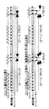
図1は本発明の第1の実施の形態における診断機能を有する半導体集積回路を構成するスキャン設計された論理回路(論理手段)100を示している。図1において、117はテストに必要な周波数のクロック信号が常時供給されるクロック端子、116はテスト開始時に回路全体を初期化するためのリセット信号が供給されるリセット端子、115はスキャンテストにおいて、シフト動作状態でスキャンデータを順次入力し、通常動作に切り替え半導体集積回路内の組合せ回路の動作をスキャンし、再びシフト動作に戻しスキャンされたデータを順次送り出すための切替信号が供給されるシフト動作/通常動作切替端子ある。また、122〜141はスキャン機能付きフリップフロップ回路、142〜157は通常動作において順序回路を構成するフリップフロップ回路間に配置された組合せ回路である。フリップフロップ回路122〜141及び組み合わせ回路142〜157のうち、相互に直列接続されたフリップフロップ回路122〜126と組み合わせ回路142〜145との組はスキャンチェーンを構成する。同様に、フリップフロップ回路127〜131、132〜136及び137〜141と組み合わせ回路146〜149、150〜153及び154〜157との組もスキャンチェーンを構成する。
【0024】
上記構成の論理回路をスキャンテストする場合、先ず、各スキャンチェーンをシフト動作に切り替え、スキャンデータ入力端子111、112、113、114からスキャンチェーンを構成する組合せ回路の故障を検出するために必要なデータを供給する。次に、各スキャンチェーンを通常動作に切り替え、1クロック分、組み合わせ回路を実動作させる。その後、各スキャンチェーンをシフト動作に戻し、スキャンデータ出力端子118、119、120、121から組合せ回路の演算結果を導出する。
【0025】
図2は本発明の第1の実施の形態における半導体集積回路に擬似乱数パルスを供給するための擬似乱数発生回路(擬似乱数発生手段)200の構成を示している。図2において、201はクロック端子、202はリセット端子、204、206、208、209はn段のシフトレジスタを構成するリセット機能付きフリップフロップ回路、207は最終n段のフリップフロップ回路の出力と任意段のフリップフロップ回路(図示例では、フリップフロップ回路208)の出力との排他的論理和を得る排他的論理和回路(EX−OR回路)である。
【0026】
シフトレジスタの初段のフリップフロップ回路204には、排他的論理和回路207の出力が供給され、最終段のフリップフロップ回路209から(2n−1)周期の擬似乱数パルスが出力される。擬似乱数発生回路200から出力される擬似乱数パルスは、バーンインテストを実行する場合に、論理回路100に印加されるストレスとして用いられる。
【0027】
図3は本発明の第1の実施の形態における診断機能を有する半導体集積回路を示しており、図1に示した論理回路100及び図2に示した擬似乱数発生回路200を備える。図3において、310はクロック端子、309はリセット端子、308はシフト動作と通常動作とを切り替えるための切替信号が供給されるシフト動作/通常動作切替端子であり、303、305、306は論理回路100をスキャンテストするためのスキャンデータが入力されるスキャンテスト入力端子である。
【0028】
論理回路100はスキャンテストの対象となるとともに、バーンインテストの対象となる。論理回路100をバーンインテストする場合、擬似乱数発生回路200で生成された擬似乱数パルスが、スキャンテスト/バーンインテスト切替端子307から供給されるスキャンテストとバーンインテストとを切り替えるための切替信号により制御されるセレクタ311、312、313を介して各スキャンチェーンに供給される。各スキャンチェーンに供給された擬似乱数パルスは、スキャンチェーン内を伝搬して判定回路(判定手段)350に導出される。
【0029】
判定回路350は各スキャンチェーンの出力値をそれぞれ予め設定された期待値と比較する。論理回路内の回路が正常に作動し、かつ回路に適切にストレスが印加されていれば、スキャンチェーンから正常な出力が導出される。判定回路350は、全てのスキャンチェーンの出力を1つに集約した判定結果を出力端子351に導出する。
【0030】
図4は図3に示した半導体集積回路を模式的に示している。すなわち、論理回路(論理手段)に対してバーンインテストを実行する場合、擬似乱数発生回路(擬似乱数発生手段)200で生成された擬似乱数パルスを論理回路を構成する複数のスキャンチェーン402〜406にそれぞれ供給し、各スキャンチェーンの出力をそれぞれ期待値と判定回路(判定手段)で比較することにより、論理回路を診断することができる。
【0031】
これにより、実動作に準ずるテストだけではストレスを印加することが難しい組み合わせ回路に対してスキャンチェーンを通じて擬似乱数パルスを供給することにより確実にストレスを印加することができる。
【0032】
以下、図5を参照して本発明の第2の実施の形態について説明する。図4に示した第1の実施の形態と異なる点は、第1の実施の形態において切替端子308から供給されるシフト動作/実動作を切り替えるための切替信号を、タイミング制御回路(タイミング制御手段)341で生成することにある。
【0033】
バーンインテストを実行する際、クロック端子310に常時テスト周波数のクロックを供給し、スキャンテスト/バーンインテスト切替端子307に切替信号を供給してバーンインテストモードに設定し、擬似乱数発生回路(擬似乱数発生手段)301から(2n−1)周期の擬似乱数パルスをセレクタ311、312を介して論理回路302を構成する各スキャンチェーンに供給する。
【0034】
タイミング制御回路341は、カウンタで生成される(2n−1)周期のタイミングパルスをデコードして各フリップフロップ回路を構成するセレクタの制御端に供給し、各フリップフロップ回路をシフト動作と通常動作とに切り替える。
【0035】
図6は、論理回路302の動作を示しており、(1)はフリップフロップ回路をシフト動作に固定する場合、(2)はフリップフロップ回路をシフト動作と通常動作とに切り替える場合を示している。
【0036】
第2の実施の形態では、タイミング制御回路341から、(2)に示すタイミングパルスを発生し、これによりフリップフロップ回路を一定周期(2n−1)毎にシフト動作と通常動作とに切り替える。
【0037】
すなわち、先ず、(2n−1)クロック期間、フリップフロップ回路をシフト動作に設定し、この状態で擬似乱数パルスをフリップフロップ回路に供給する。次に、1クロック期間、フリップフロップ回路を通常動作に設定し、この状態で、供給された擬似乱数パルスを処理する。その後、再び、(2n−1)クロック期間、フリップフロップ回路をシフト動作に設定し、この状態で、擬似乱数パルスをシフトさせる。この動作を繰り返して、供給された擬似乱数パルスを判定回路350に導出する。なお、バーンインテストが実行されている場合は、スキャンデータ入力端子に入力されるスキャンデータは第1の極性(正極性)若しくは第2の極性(負極性)に設定される。
【0038】
上述のように、バーンインテストを実行する場合、論理回路を構成するスキャンチェーンをシフト動作に固定せずに、シフト動作と通常動作とに切り替えることにより、フリップフロップ回路間の組み合わせ回路に対してもストレスが印加される。従って、論理回路に対するストレスの印加率を高めることができ、効率よくストレスを印加することができる。
【0039】
以下、図7を参照して第3の実施の形態における半導体集積回路について説明する。論理回路を構成する複数のスキャンチェーンに対して擬似乱数パルスを供給する場合、第1及び第2の実施の形態では、擬似乱数発生回路及び判定回路に対して各スキャンチェーンが並列に接続され、各スキャンチェーンに同時に擬似乱数パルスが供給されていたのに対し、第3の実施の形態では、擬似乱数発生回路501及び判定回路507に対して複数のスキャンチェーン501〜506が互いに直列に接続され、各スキャンチェーンに順次擬似乱数パルスが供給される。最終のスキャンチェーン526から導出された擬似乱数パルスは、判定回路507に供給される。
【0040】
第1及び第2の実施の形態では、判定回路は各スキャンチェーンから出力される複数の出力値をそれぞれ期待値と比較し、その後、複数の比較結果に基づいて論理回路の状態を判定している。しかし、第3の実施の形態では、判定回路507は1つの出力値を期待値と比較するだけで、複数のスキャンチェーンを有する論理回路の状態を判定することができるため、判定回路507の判定処理を簡易化することができる。
【0041】
以下、図8を参照して第4の実施の形態について説明する。図8において、601は乱数パルスを発生する乱数発生回路(乱数発生手段)、609は常時バーンインテスト周波数のクロックが供給されるクロック端子、608はバーンインテスト開始時に半導体集積回路全体を初期化するためのリセット信号が入力されるリセット端子、607はシフト動作と通常動作とを切り替える切替信号が供給されるシフト動作/通常動作切替端子、603、604、605、606はスキャンデータが供給されるスキャンデータ入力端子である。また、628〜655はスキャン機能付きフリップフロップ回路、656〜679は通常動作において順序回路を構成するスキャン機能付きフリップフロップ回路間の組合せ回路であり、互いに直接接続されたフリップフロップ回路及び組み合わせ回路はスキャンチェーンを構成する。
【0042】
バーンインテストを実行する場合、フリップフロップ回路628〜655を構成する各セレクタをシフト動作に切り替え、かつスキャンデータ入力端子に供給されるスキャンデータを第1の極性(正極性)又は第2の極性(負極性)に設定する。この状態で、乱数発生回路601で生成された乱数パルスを各スキャンチェーンを介して判定部610、611に導出する。判定部610,611は、各スキャンチェーンの出力値を論理演算により比較する。
【0043】
いま、フリップフロップ回路628から始まるスキャンチェーン(第1のスキャンチェーン)と、フリップフロップ回路635から始まるスキャンチェーン(第2のスキャンチェーン)とに着目する。各スキャンチェーンにはそれぞれ同一の擬似乱数パルスが供給されるため、各スキャンチェーンにおいて、擬似乱数パルスが同一段数分シフトされて導出される出力値は互いに同一である。従って、これら出力値を比較することにより、各スキャンチェーンが正常に動作しているか、若しくは適切なストレスが印加されているか否かを判別することができる。
【0044】
判定部610は、第1及び第2のスキャンチェーンの同一段目のフリップフロップ回路の出力値の排他的論理和を順次得、各排他的論理和の論理積を得る。すなわわち、第1のスキャンチェーンを構成するフリップフロップ回路631の出力値と第2のスキャンチェーンを構成するフリップフロップ回路638の出力値とをEX−OR回路620に入力する。同様に、フリップフロップ回路632の出力値とフリップフロップ回路639の出力値とをEX−OR回路621に入力し、フリップフロップ回路633の出力値とフリップフロップ回路640の出力値とをEX−OR回路622に入力し、フリップフロップ回路634の出力値とフリップフロップ回路641の出力値とをEX−OR回路623に入力する。各EX−OR回路の出力はそれぞれAND回路618に入力される。これにより、第1及び第2のスキャンチェーンの出力が一致しているか否かが確認される。このとき第1及び第2のスキャンチェーンを構成するそれぞれのフリップフロップ回路の段数を一致させ、かつ各スキャンチェーンを第1の極性(正極性)又は第2の極性(負極性)に統一してスキャンチェーンを構成することにより、2つのスキャンチェーンの出力を比較する回路を簡略化することが可能となる。
【0045】
フリップフロップ回路642から始まるスキャンチェーン及びフリップフロップ回路649から始まるスキャンチェーンについても、同様に各スキャンチェーンを構成する同一段目のフリップフロップ回路の出力値を互いに比較し、各段目のフリップフロップ回路の出力値の比較結果の論理積を得ることにより、2つのスキャンチェーンの出力が一致しているか否かが確認される。
【0046】
AND回路618、619に出力はAND回路614に集約され、その論理積が出力端子615に導出される。これにより、論理回路の動作状態若しくは論理回路のストレス印加状態を確認することができる。
【0047】
図9は第4の実施の形態を模式的に示している。すなわち、乱数発生回路701で生成された乱数パルスが、互いに同一段数のスキャンチェーン(m段)702、703に供給される。そして、各スキャンチェーンの最終段からn段分のフリップフロップ回路(判定対象)の出力706、707を判定部710で比較する。同様に、乱数パルスが互いに同一段数のスキャンチェーン(k段)704、705に供給される。そして、各スキャンチェーンの最終段からn段分のフリップフロップ回路(判定対象)の出力708、709を判定部711で比較する。各判定部の出力はAND回路712に入力され、各出力の論理積を得ることにより、論理回路の動作状態、若しくは論理回路のストレス印加状態を確認することができる。
【0048】
図10は第4の実施の形態の応用例を模式的に示したものである。乱数発生回路801で生成された乱数パルスは互いに同一段数のスキャンチェーン(m段)802、803、804に供給される。そして、各スキャンチェーンの最終段からn段分のフリップフロップ回路(判定対象)の出力810、811、812を判定部818で比較する。判定部818は、図示例のように、フリップフロップ回路の出力812とフリップフロップ回路の出力810、811とを比較する他、出力810と出力811、812とを比較、又は出力811と出力810、812とを比較するようにしてもよい。
【0049】
同様に、乱数パルスが互いに同一段数のスキャンチェーン(k段)805、806、807に供給される。そして、各スキャンチェーンの最終段からn段分のフリップフロップ回路(判定対象)の出力813、814、815を判定部819で比較する。さらに、乱数パルスがスキャンチェーン(z段)808、809に供給され、各スキャンチェーンの最終段からn段分のフリップフロップ回路(判定対象)の出力816、817を判定部820で比較する。各判定部の出力はAND回路812に入力され、各出力の論理積を得ることにより、論理回路の動作状態、若しくは論理回路のストレス印加状態を確認することができる。
【0050】
図10に示した構成によれば、構成段数が同一のスキャンチェーン同士の出力を互いに比較するため、構成段数が揃っている設計モジュール単位或いはレイアウト時のブロック単位毎に回路をテストすることができる。従って、テスト回路の設計が容易となる。また、モジュール単位で出力を判定することができるため、複数のモジュールの各出力を集約することにより、リアルタイムで1チップの出力判定が可能となる。
【0051】
以下、図11を参照して第5の実施の形態について説明する。図11において、910はバーンインテストに必要な周波数を有するクロックが常時供給されるクロック端子、909は半導体集積回路全体を初期化する初期化信号が入力されるリセット端子、913〜927はスキャン機能付きフリップフロップ回路、928〜939は組合せ回路、908はシフト動作と通常動作とを切り替える切替信号が入力されるシフト動作/通常動作切替端子、907はスキャンテストとバーンインテストとに切り替える切替信号が入力されるスキャンテスト/バーンインテスト切替端子である。
【0052】
バーンインテストを実行する場合は、リセット端子909に入力される初期化信号により半導体集積回路を初期化し、スキャンテスト/バーンインテスト切替端子907を介して入力される切替信号を第1の極性(正極性)又は第2の極性(負極性)に設定してセレクタ911、912、913をバーンインテストモードに切り替えて、擬似乱数発生回路901で生成された擬似乱数パルスを論理回路902を構成する各スキャンチェーンに供給する。
【0053】
なお、必要に応じて、第2の実施の形態に示したように、スキャンチェーンを所定周期毎にシフト動作と通常動作とに切り替えてるようにしてもよい。各スキャンチェーンを通過した擬似乱数パルスはそれぞれ判定回路946に供給され、回路の動作状態及びストレスの印加状態が判定される。
【0054】
第5の実施の形態では、図示のように、出力端子941、943にスキャンチェーンを構成する最終段のフリップフロップ回路の出力が供給され、出力端子940にはスキャンチェーンを構成する組み合わせ回路の出力が供給される。また、入力部と出力部とを有する入出力端子944は、スキャンチェーンを構成する組み合わせ回路の出力により出力モードに設定された状態で最終段のフリップフロップ回路の出力が外部導出される。さらに、この出力は、入出力端子944を構成する入力部を介して別のスキャンチェーン内の組み合わせ回路に供給される。
【0055】
上記構成により、スキャンチェーンに接続される出力端子、入出力端子を含めて半導体集積回路全体にストレスを印加することができる。なお、出力端子940、941、943には単にストレスが印加されるのみであるが、バーンインテスト後の別のテストにおいて出力端子にストレスを印加した結果が反映される。
【0056】
以下、図12を参照して第6の実施の形態について説明する。図11において、1104はシフト動作と通常動作とを切り替える切替信号が入力されるシフト動作/通常動作切替端子、1105はバーンインテスト開始時に半導体集積回路全体を初期化する初期化信号が入力されるリセット端子、1107はバーンインテストに必要な周波数のクロックが常時供給されるクロック端子、1108はバーンインテストモードを設定する設定信号が入力されるバーンインテスト設定端子、1113〜1122はスキャン機能付きフリップフロップ回路、1123〜1130は組み合わせ回路である。
【0057】
第6の実施の形態では、シフト動作/通常動作切替端子1104、リセット端子1105、クロック信号入力1107及びバーンインテスト設定端子1108以外の入力端子が、全て入出力端子で置き換えられる。すなわち、擬似乱数発生回路1101で生成された擬似乱数パルス又はスキャンデータが供給される入出力端子1103、1106が設けられる。各スキャンチェーンを通過した擬似乱数パルスはそれぞれ判定回路1112に供給され、回路の動作状態及びストレスの印加状態が判定される。
【0058】
バーンインテストを実行する場合、バーンインテスト設定端子1108に入力される設定信号を第1の極性(正極性)又は第2の極性(負極性)に設定してセレクタ1102をバーンインテストモードに設定する。セレクタ1102の出力は入出力部1103、1106を構成する出力部の制御端に供給されている。セレクタ1102がバーンインテストモードが設定されると、入出力部1103、1106が入力モードに設定され、擬似乱数パルスが入出力部1103、1106を介して各スキャンチェーンに供給される。これにより、入出力端子1103、1106及び半導体集積回路を構成するスキャンチェーンにストレスを印加することができる。
【0059】
半導体集積回路の出力側において、出力端子1110にはスキャンチェーンを構成する最終段のフリップフロップ回路の出力が供給される。入出力端子1109はセレクタ1102により、バーンインテスト実行時、出力モードに設定され、スキャンチェーンの出力が外部導出されるとともに、入力部を介して別のスキャンチェーンに供給される。
【0060】
上記構成により、出力端子、入出力端子を含めて半導体集積回路全体にストレスを印加することができる。
【0061】
なお、第6の実施の形態において、半導体集積回路の入力側の端子にのみストレスを印加するようにしてもよい。
【0062】
【発明の効果】
請求項1及び2に記載の発明によれば、論理手段の動作状態、ストレス印加状態を確認するための判定手段が、各論理手段の出力に対して個々に比較し、全ての論理手段に対する比較結果を1つの判定結果として出力することにより、半導体集積回路から出力される判定手段の判定結果が1つに集約されるため、半導体集積回路を診断するために必要とされる端子数を最小限に抑えることができ、かつ1つの判定結果によって複数の論理手段を確実に診断することができる。また、判定結果をモニタするための外部装置においても、判定手段で集約された1つの判定結果に基づいて、半導体集積回路の不具合を確認することができ、診断装置全体のコストを抑えることができる。さらに、論理手段に供給された擬似乱数パルスのシフト動作に加えて通常動作を加えることにより、論理手段に印加されるストレスの度合いを高めることができ、より効率的なストレス印加が可能となる。
【0063】
請求項3に記載の発明によれば、さらに、複数の論理手段を直列接続し、擬似乱数発生手段から判定手段までの経路を一本化して、擬似乱数パルスの供給及び論理手段の判定手段への出力を一元化することにより、特に、判定手段にあっては、複数の論理手段の出力を1度に比較することができる。従って、判定手段の簡易化を図ることができる。
【0065】
請求項4に記載の発明によれば、同一構成の複数の論理手段の出力を相互に比較対象としているため、乱数パルスに基づいて算出される期待値等を用意することがなく、判定手段を簡易化することができる。判定手段からは、各出力値に対する比較結果を1つの判定結果として出力されるので、半導体集積回路から出力される判定手段の判定結果が1つに集約され、これにより、半導体集積回路を診断するために必要とされる端子数を削減す最小限に抑えることができ、かつ1つの判定結果によって複数の論理手段を確実に診断することができる。また、判定結果をモニタするための外部装置においても、判定手段で集約された1つの判定結果に基づいて、半導体集積回路の不具合を確認することができ、診断装置全体のコストを抑えることができる。
【0066】
請求項5及び6に記載の発明によれば、さらに、論理手段に接続される端子に対してもストレスを印加し、これら端子を含めた半導体集積回路全体にストレスを印加することにより、半導体集積回路を構成する論理手段だけでなく端子もストレス印加による診断対象とすることができ、より精度の高い診断を実行することができる。
【図面の簡単な説明】
【図1】本発明の第1の実施の形態における診断機能を有する半導体集積回路を構成する論理回路100を示す構成図である。
【図2】本発明の第1の実施の形態における診断機能を有する半導体集積回路を構成する擬似乱数発生回路200を示す構成図である。
【図3】本発明の第1の実施の形態における診断機能を有する半導体集積回路を示す構成図である。
【図4】本発明の第1の実施の形態における診断機能を有する半導体集積回路を示す模式図である。
【図5】本発明の第2の実施の形態における診断機能を有する半導体集積回路を示す構成図である。
【図6】図5で示した論理回路302の動作を示すタイミングチャートである。
【図7】本発明の第3の実施の形態における診断機能を有する半導体集積回路を示す構成図である。
【図8】本発明の第4の実施の形態における診断機能を有する半導体集積回路を示す構成図である。
【図9】第4の実施の形態を示す模式図である。
【図10】第4の実施の形態の変形例を示す構成図である。
【図11】本発明の第5の実施の形態における診断機能を有する半導体集積回路を示す構成図である。
【図12】本発明の第6の実施の形態における診断機能を有する半導体集積回路を示す構成図である。
【符号の説明】
100 論理回路(論理手段)
111〜114 スキャンデータ入力端子
115 シフト動作/通常動作モード切替端子
116 リセット端子
117 クロック端子
118〜121 スキャンデータ出力端子
122〜141 スキャン機能付きフリップフロップ回路
142〜157 組み合わせ回路
200 擬似乱数発生回路
201 クロック端子
202 リセット端子
204、206、208、209 フリップフロップ回路
207 EX−OR(排他的論理和)回路
210 擬似乱数出力端子
303、305、306 スキャンデータ入力端子
307 スキャンテスト/バーンインテスト切替端子
308 シフト動作/通常動作切替端子
309 リセット端子
310 クロック端子
311〜313 セレクタ
314〜327 スキャン機能付きフリップフロップ回路
328〜339 組み合わせ回路
341 タイミング制御回路
350 判定回路
351 出力端子
402〜406 スキャンチェーン
501 擬似乱数発生回路
502〜506 スキャンチェーン
507 判定回路
601 乱数発生回路
603〜606 スキャンデータ入力端子
607 シフト動作/通常動作切替端子
608 リセット端子
609 クロック端子
610、611 判定部
612、613、616、617 スキャンデータ出力端子
614、618、619 AND回路
615 出力端子
628〜655 フリップフロップ回路
656〜679 組み合わせ回路
701 乱数発生回路
702〜705 スキャンチェーン
710、711 判定部
712 AND回路
801 乱数発生回路
802〜809 スキャンチェーン
818、819、820 判定部
821 AND回路
901 擬似乱数発生回路
903〜906 スキャンチェーン
907 スキャンテスト/バーンインテスト切替端子
908 シフト動作/通常動作切替端子
909 リセット端子
910 クロック端子
911〜913 セレクタ
914〜927 フリップフロップ回路
928〜939 組み合わせ回路
940、941、943、945 出力端子
944 入出力端子
946 判定回路
1101 擬似乱数発生回路
1102 セレクタ
1103、1106、1109 入出力端子
1104 シフト動作/通常動作切替端子
1105 リセット端子
1107 クロック端子
1108 バーンインテスト設定端子
1110、1111 出力端子
1112 判定回路
1113〜1122 フリップフロップ回路
1123〜1130 組み合わせ回路[0001]
TECHNICAL FIELD OF THE INVENTION
The present invention relates to a semiconductor integrated circuit having a scan-designed logic circuit and having a diagnostic function of diagnosing the logic circuit.
[0002]
[Prior art]
2. Description of the Related Art In recent years, as semiconductor integrated circuits have become larger in scale and have become synchronous circuits, circuit design by logic synthesis using function descriptions and scan design methods have attracted attention as methods for automatically creating test patterns. Further, in high-performance system LSIs (large-scale integrated circuits), reliability tests such as burn-in tests have become increasingly important. On the other hand, in this high-performance system LSI, it is extremely difficult to completely realize the state of actually operating on the set device at the time of a test. A huge problem is that the input device of the application or test vector is enormously expensive. Therefore, stress is often applied to the circuit by using the scan design method.
[0003]
Pseudo-stress application using the scan design method means that test patterns are designed in a manner that is as practical as possible in the actual operation mode in the actual use mode, and that the power consumption measurement, In order to achieve a circuit operation rate equivalent to the real mode with a limited pattern length compared to the stress application method in the reliability test, a method of creating an equivalent test pattern by scan design method etc. and introducing it to the test It is.
[0004]
Although this is not equivalent to the actual operation state, it is possible to make the ratio of the operating circuits in the semiconductor integrated circuit close to the actual operation in the reliability test, etc. Thus, it is possible to prevent the test from being performed without applying a sufficient stress.
[0005]
Hereinafter, a conventional burn-in test will be described. The conventional burn-in test has been performed on packaged finished products, so when testing, dozens of signal supply sources with different frequencies are supplied from the outside by the required number of terminals, and internal signals are supplied. The method of operating the circuit was adopted. At this time, a pattern close to the actual operation could be realized by a combination of signal supply sources for a circuit having a small-scale semiconductor integrated circuit and an operationally uncomplicated one.
[0006]
However, as semiconductor integrated circuits have become larger and more complex, it has become impossible to realize actual operation with a combination of prepared signal supply sources. Has been realized and replaced by a combination of signal supply sources.
[0007]
[Problems to be solved by the invention]
The burn-in test is usually performed on a large number of semiconductor integrated circuits at a time, but a considerable amount of equipment is required to properly apply a specific stress to a large number of semiconductor integrated circuits. . Further, a device for monitoring the output result with respect to the applied stress also becomes large-scale. Further, as the number of terminals provided increases as the scale of the semiconductor integrated circuit increases, the size of the device also increases accordingly, leading to a significant increase in cost.
[0008]
On the other hand, a burn-in test for a semiconductor integrated circuit has been established in recent years, in addition to a finished product, at a wafer level. However, since a burn-in test at the wafer level simultaneously tests a much larger number of semiconductor integrated circuits than a test performed on a finished product, it is necessary to test each semiconductor integrated circuit. The number of usable terminals is limited. Therefore, a circuit design that can apply stress and observe the state with a limited number of terminals is required.
[0009]
The present invention has been made in view of the above circumstances, and minimizes the number of terminals required when diagnosing a semiconductor integrated circuit, and provides a semiconductor integrated circuit having a diagnostic function capable of performing reliable diagnosis. The purpose is to provide.
[0010]
[Means for Solving the Problems]
The present invention according to
[0011]
According to a second aspect of the present invention, the logic unit is connected in parallel to the pseudorandom number generation unit and the determination unit.
[0012]
According to a third aspect of the present invention, the logic unit is connected in series to the pseudorandom number generation unit and the determination unit.
[0014]
Claim4The present invention according to the present invention is a random number generating means for generating a random number pulse, a plurality of logic means scan path designed having the same number of flip-flop circuits each supplied with the random number pulse and configured to shift operation, Among the logic means, at least one output value of each flip-flop circuit of the same stage is compared with each other to determine whether or not each value matches each other, and based on a determination result for all output values, Determining means for outputting a determination result.
[0015]
Claim5The present invention according to the present invention has at least one terminal connected to the logic means so as to externally output an output of a final stage and / or an internal combinational circuit of the logic means, and at least one of the terminals is An input / output terminal that has an input unit and an output unit, and outputs the output of the last stage and / or internal circuit of the logic unit supplied to the output unit to any logic unit via the input unit. Things.
[0016]
Claim6The present invention relates to a pseudo random number pulse having an input unit and an output unit, connected to the logic unit for supplying data to the logic unit via the input unit, and supplied to the output unit. Alternatively, it has an input / output terminal capable of supplying a random number pulse to the logic means via the input section.
[0017]
According to the first and second aspects of the present invention, an operation state of the logic means and a logic means are provided by applying a pseudo-random number pulse to the logic means, applying a stress, and comparing the output of the logic means with an expected value by the determination means. This confirms the state of stress application. The determination means compares the outputs of the respective logic means individually, and outputs the comparison result for all the logic means as one determination result. Thereby, the determination result of the determination unit output from the semiconductor integrated circuit is consolidated into one, so that the number of terminals required for diagnosing the semiconductor integrated circuit can be reduced.In addition, by applying a normal operation in addition to the shift operation of the pseudo random number pulse supplied to the logic means, the degree of stress applied to the logic means can be increased, and more efficient stress application becomes possible.
[0018]
According to a third aspect of the present invention, a plurality of logic means are connected in series, and a single path from the pseudo-random number generation means to the determination means is integrated to supply a pseudo-random number pulse and output the logic means to the determination means. Is unified. Thereby, in particular, in the determination means, the outputs of the plurality of logic means can be compared at one time, while the outputs of the plurality of logic means are individually compared. Therefore, the determination means can be simplified.
[0020]
Claim4The invention described in (1) supplies a random number pulse to the logic means having the same number of stages, compares the output values of the flip-flop circuits of the same stage of each logic means with each other, and checks the operation state of the logic means and the stress of the logic means. This is to check the applied state. This comparison can be performed on the output value of the flip-flop circuit at each stage. The determination means outputs a plurality of comparison results for each stage as one determination result. Claim4In the invention described in (1), since the outputs of a plurality of logic means having the same configuration are compared with each other, it is possible to simplify the determination means without preparing an expected value calculated based on the random number pulse. it can. The judging means outputs a comparison result for each output value as one judgment result. Thereby, the determination result of the determination unit output from the semiconductor integrated circuit is consolidated into one, so that the number of terminals required for diagnosing the semiconductor integrated circuit can be reduced.
[0021]
Claim5as well as6According to the invention described in (1), stress is also applied to terminals connected to the logic means, and stress is applied to the entire semiconductor integrated circuit including these terminals. As a result, not only the logic means constituting the semiconductor integrated circuit but also the terminals can be subjected to the diagnosis by applying the stress, so that a more accurate diagnosis can be executed.
[0022]
In the present invention, the logic means includes a scan chain structure in which a scan function designed flip-flop circuit with a scan function and a combinational circuit arranged between these circuits are cascaded, and one scan chain structure Or a plurality of logic units having one or a plurality of scan chain structures.
[0023]
BEST MODE FOR CARRYING OUT THE INVENTION
Hereinafter, embodiments of the present invention will be described with reference to the drawings.
FIG. 1 shows a scan-designed logic circuit (logic means) 100 constituting a semiconductor integrated circuit having a diagnostic function according to a first embodiment of the present invention. In FIG. 1,
[0024]
When performing a scan test on the logic circuit having the above configuration, first, each scan chain is switched to the shift operation, and the scan
[0025]
FIG. 2 shows a configuration of a pseudo random number generation circuit (pseudo random number generation means) 200 for supplying a pseudo random number pulse to the semiconductor integrated circuit according to the first embodiment of the present invention. 2,
[0026]
The output of the exclusive OR
[0027]
FIG. 3 shows a semiconductor integrated circuit having a diagnostic function according to the first embodiment of the present invention, which includes the
[0028]
The
[0029]
The
[0030]
FIG. 4 schematically shows the semiconductor integrated circuit shown in FIG. That is, when performing a burn-in test on a logic circuit (logic means), the pseudo random number pulse generated by the pseudo random number generation circuit (pseudo random number generation means) 200 is sent to a plurality of
[0031]
As a result, it is possible to reliably apply the stress by supplying the pseudo-random number pulse through the scan chain to the combinational circuit in which it is difficult to apply the stress only by the test according to the actual operation.
[0032]
Hereinafter, a second embodiment of the present invention will be described with reference to FIG. The difference from the first embodiment shown in FIG. 4 is that the switching signal for switching between the shift operation and the actual operation supplied from the switching
[0033]
When executing the burn-in test, a clock of a test frequency is always supplied to the
[0034]
The
[0035]
6A and 6B show the operation of the
[0036]
In the second embodiment, a timing pulse shown in (2) is generated from the
[0037]
That is, first, (2n-1) The flip-flop circuit is set to the shift operation during the clock period, and a pseudo random number pulse is supplied to the flip-flop circuit in this state. Next, the flip-flop circuit is set to the normal operation for one clock period, and the supplied pseudo random number pulse is processed in this state. Then, again, (2n-1) The flip-flop circuit is set to the shift operation during the clock period, and the pseudo random number pulse is shifted in this state. By repeating this operation, the supplied pseudo random number pulse is derived to the
[0038]
As described above, when performing the burn-in test, the scan chain forming the logic circuit is not fixed to the shift operation, but is switched between the shift operation and the normal operation, so that the combination circuit between the flip-flop circuits is also performed. Stress is applied. Therefore, the stress application rate to the logic circuit can be increased, and the stress can be efficiently applied.
[0039]
Hereinafter, a semiconductor integrated circuit according to the third embodiment will be described with reference to FIG. In the case of supplying a pseudo-random number pulse to a plurality of scan chains constituting a logic circuit, in the first and second embodiments, each scan chain is connected in parallel to the pseudo-random number generation circuit and the determination circuit, While pseudo-random number pulses are simultaneously supplied to each scan chain, in the third embodiment, a plurality of
[0040]
In the first and second embodiments, the determination circuit compares a plurality of output values output from each scan chain with an expected value, and then determines the state of the logic circuit based on the plurality of comparison results. I have. However, in the third embodiment, the
[0041]
Hereinafter, the fourth embodiment will be described with reference to FIG. In FIG. 8,
[0042]
When performing the burn-in test, the selectors constituting the flip-
[0043]
Attention is now focused on a scan chain (first scan chain) starting from the flip-
[0044]
The
[0045]
Similarly, regarding the scan chain starting from the flip-
[0046]
The outputs of the AND
[0047]
FIG. 9 schematically shows the fourth embodiment. That is, the random number pulse generated by the random
[0048]
FIG. 10 schematically shows an application example of the fourth embodiment. The random number pulses generated by the random
[0049]
Similarly, random number pulses are supplied to the same number of scan chains (k stages) 805, 806, and 807. The
[0050]
According to the configuration shown in FIG. 10, since the outputs of scan chains having the same number of stages are compared with each other, it is possible to test the circuit for each design module having the same number of stages or for each block during layout. . Therefore, the design of the test circuit becomes easy. Further, since the output can be determined for each module, the output of one chip can be determined in real time by aggregating the outputs of a plurality of modules.
[0051]
Hereinafter, the fifth embodiment will be described with reference to FIG. In FIG. 11,
[0052]
To execute the burn-in test, the semiconductor integrated circuit is initialized by the initialization signal input to the
[0053]
If necessary, as described in the second embodiment, the scan chain may be switched between a shift operation and a normal operation at predetermined intervals. The pseudo-random number pulse that has passed through each scan chain is supplied to the
[0054]
In the fifth embodiment, as shown, the
[0055]
With the above structure, stress can be applied to the entire semiconductor integrated circuit including the output terminal and the input / output terminal connected to the scan chain. Although stress is simply applied to the
[0056]
Hereinafter, the sixth embodiment will be described with reference to FIG. In FIG. 11,
[0057]
In the sixth embodiment, input terminals other than the shift operation / normal operation switching terminal 1104, the
[0058]
When performing the burn-in test, the setting signal input to the burn-in test setting terminal 1108 is set to the first polarity (positive polarity) or the second polarity (negative polarity), and the
[0059]
On the output side of the semiconductor integrated circuit, an
[0060]
With the above structure, stress can be applied to the entire semiconductor integrated circuit including the output terminal and the input / output terminal.
[0061]
In the sixth embodiment, the stress may be applied only to the terminal on the input side of the semiconductor integrated circuit.
[0062]
【The invention's effect】
According to the first and second aspects of the present invention, the judging means for confirming the operation state and the stress application state of the logic means individually compares the outputs of the respective logic means, and compares the outputs of all the logic means. By outputting the result as one judgment result, the judgment results of the judgment means output from the semiconductor integrated circuit are integrated into one, so that the number of terminals required for diagnosing the semiconductor integrated circuit is minimized. , And a plurality of logic means can be diagnosed reliably by one determination result. In addition, even in an external device for monitoring the determination result, the failure of the semiconductor integrated circuit can be confirmed based on one determination result collected by the determination unit, and the cost of the diagnostic device as a whole can be suppressed. .Further, by applying a normal operation in addition to the shift operation of the pseudo random number pulse supplied to the logic means, the degree of stress applied to the logic means can be increased, and more efficient stress application becomes possible.
[0063]
According to the third aspect of the present invention, furthermore, a plurality of logic means are connected in series, the path from the pseudorandom number generation means to the determination means is unified, and the pseudorandom number pulse is supplied to the determination means of the logic means. In particular, in the determination means, the outputs of a plurality of logic means can be compared at one time by unifying the outputs of. Therefore, the determination means can be simplified.
[0065]
Claim4According to the invention described in (1), since the outputs of a plurality of logic units having the same configuration are compared with each other, an expected value or the like calculated based on a random number pulse is not prepared, and the determination unit is simplified. be able to. Since the determination unit outputs a comparison result for each output value as one determination result, the determination results of the determination unit output from the semiconductor integrated circuit are combined into one, and thereby the semiconductor integrated circuit is diagnosed. Therefore, the number of terminals required can be reduced to a minimum, and a plurality of logic means can be diagnosed reliably by one determination result. In addition, even in an external device for monitoring the determination result, the failure of the semiconductor integrated circuit can be confirmed based on one determination result collected by the determination unit, and the cost of the diagnostic device as a whole can be suppressed. .
[0066]
Claim5as well as6According to the invention described in (1), further, stress is applied to the terminals connected to the logic means, and stress is applied to the entire semiconductor integrated circuit including these terminals, whereby the logic constituting the semiconductor integrated circuit is formed. Not only the means but also the terminals can be subjected to the diagnosis by the application of stress, so that a more accurate diagnosis can be executed.
[Brief description of the drawings]
FIG. 1 is a configuration diagram showing a
FIG. 2 is a configuration diagram showing a pseudo-random
FIG. 3 is a configuration diagram illustrating a semiconductor integrated circuit having a diagnostic function according to the first embodiment of the present invention.
FIG. 4 is a schematic diagram showing a semiconductor integrated circuit having a diagnostic function according to the first embodiment of the present invention.
FIG. 5 is a configuration diagram illustrating a semiconductor integrated circuit having a diagnostic function according to a second embodiment of the present invention.
FIG. 6 is a timing chart showing an operation of the
FIG. 7 is a configuration diagram illustrating a semiconductor integrated circuit having a diagnostic function according to a third embodiment of the present invention.
FIG. 8 is a configuration diagram illustrating a semiconductor integrated circuit having a diagnostic function according to a fourth embodiment of the present invention.
FIG. 9 is a schematic diagram showing a fourth embodiment.
FIG. 10 is a configuration diagram illustrating a modification of the fourth embodiment.
FIG. 11 is a configuration diagram illustrating a semiconductor integrated circuit having a diagnostic function according to a fifth embodiment of the present invention.
FIG. 12 is a configuration diagram illustrating a semiconductor integrated circuit having a diagnostic function according to a sixth embodiment of the present invention.
[Explanation of symbols]
100 Logic circuit (logic means)
111-114 scan data input terminal
115 shift operation / normal operation mode switching terminal
116 Reset terminal
117 Clock terminal
118-121 Scan data output terminal
122-141 Flip-Flop Circuit with Scan Function
142-157 Combination circuit
200 Pseudo random number generation circuit
201 clock terminal
202 Reset terminal
204, 206, 208, 209 flip-flop circuits
207 EX-OR (Exclusive OR) circuit
210 pseudo random number output terminal
303, 305, 306 scan data input terminal
307 Scan test / burn-in test switching terminal
308 shift operation / normal operation switching terminal
309 Reset terminal
310 clock terminal
311 to 313 Selector
314-327 Flip-flop circuit with scan function
328-339 Combination circuit
341 Timing control circuit
350 judgment circuit
351 output terminal
402-406 scan chain
501 Pseudo random number generation circuit
502-506 scan chain
507 judgment circuit
601 random number generation circuit
603 to 606 scan data input terminal
607 Shift operation / normal operation switching terminal
608 Reset terminal
609 clock terminal
610, 611 judgment part
612, 613, 616, 617 Scan data output terminal
614, 618, 619 AND circuit
615 output terminal
628-655 flip-flop circuit
656-679 Combination circuit
701 Random number generator
702-705 scan chain
710, 711 judgment part
712 AND circuit
801 random number generator
802-809 scan chain
818, 819, 820 Judgment unit
821 AND circuit
901 pseudorandom number generation circuit
903-906 scan chain
907 Scan test / burn-in test switching terminal
908 shift operation / normal operation switching terminal
909 Reset terminal
910 clock terminal
911-913 selector
914-927 Flip-flop circuit
928-939 Combination circuit
940, 941, 943, 945 output terminal
944 input / output terminal
946 judgment circuit
1101 Pseudo random number generation circuit
1102 Selector
1103, 1106, 1109 I / O terminal
1104 Shift operation / normal operation switching terminal
1105 Reset terminal
1107 Clock terminal
1108 Burn-in test setting terminal
1110, 1111 output terminal
1112 Judgment circuit
1113 to 1122 flip-flop circuits
1123-1130 Combination circuit
Claims (6)
前記擬似乱数パルスが供給され、シフト動作と通常動作とが実行可能に構成された複数のフリップフロップ回路を有するスキャンパス設計された少なくとも1つの論理手段と、
前記論理手段の出力値と予め設定された期待値とを比較して各値が互いに一致するか否かを判定し、全ての論理手段に対する判定結果に基づいて1つの判定結果を出力する判定手段と、を具備し、
前記擬似乱数パルスの周期で一巡するタイミングパルスを生成するタイミング制御手段を有し、前記論理手段が、前記タイミングパルスに基づいて、前記擬似乱数パルスの1周期期間設定されるシフト動作と、少なくとも1クロック期間設定される通常動作とがを順次実行することを特徴とする診断機能を有する半導体集積回路。Pseudo-random number generating means for generating a pseudo-random number pulse of a predetermined cycle;
At least one scan path-designed logic means having a plurality of flip-flop circuits supplied with the pseudo-random number pulse and capable of performing a shift operation and a normal operation;
Determining means for comparing the output value of the logic means with a preset expected value to determine whether or not the respective values match each other, and outputting one determination result based on the determination results for all the logic means; And comprising
Timing control means for generating a timing pulse that makes a cycle at a cycle of the pseudo-random number pulse, wherein the logic means performs a shift operation that is set for one period of the pseudo-random number pulse based on the timing pulse; A semiconductor integrated circuit having a diagnostic function, wherein a normal operation set for a clock period is sequentially performed .
前記乱数パルスが供給され、シフト動作可能に構成されたそれぞれ同一段数のフリップフロップ回路を有するスキャンパス設計された複数の論理手段と、
前記論理手段のうち、それぞれ同一段目のフリップフロップ回路の複数の出力値を互いに比較して各値が互いに一致するか否かを判定し、全ての出力値に対する判定結果に基づいて1つの判定結果を出力する判定手段と、
を具備したことを特徴とする診断機能を有する半導体集積回路。Random number generating means for generating a random number pulse;
A plurality of scan path-designed logic means having the same number of flip-flop circuits each configured to be supplied with the random number pulse and capable of performing a shift operation,
Among the logic means, a plurality of output values of the flip-flop circuit of the same stage are compared with each other to determine whether or not each value matches each other, and one determination is made based on a determination result for all output values. Determining means for outputting a result;
A semiconductor integrated circuit having a diagnostic function, comprising:
Priority Applications (1)
| Application Number | Priority Date | Filing Date | Title |
|---|---|---|---|
| JP36316699A JP3601774B2 (en) | 1999-12-21 | 1999-12-21 | Semiconductor integrated circuit having diagnostic function |
Applications Claiming Priority (1)
| Application Number | Priority Date | Filing Date | Title |
|---|---|---|---|
| JP36316699A JP3601774B2 (en) | 1999-12-21 | 1999-12-21 | Semiconductor integrated circuit having diagnostic function |
Publications (2)
| Publication Number | Publication Date |
|---|---|
| JP2001174518A JP2001174518A (en) | 2001-06-29 |
| JP3601774B2 true JP3601774B2 (en) | 2004-12-15 |
Family
ID=18478661
Family Applications (1)
| Application Number | Title | Priority Date | Filing Date |
|---|---|---|---|
| JP36316699A Expired - Fee Related JP3601774B2 (en) | 1999-12-21 | 1999-12-21 | Semiconductor integrated circuit having diagnostic function |
Country Status (1)
| Country | Link |
|---|---|
| JP (1) | JP3601774B2 (en) |
Families Citing this family (2)
| Publication number | Priority date | Publication date | Assignee | Title |
|---|---|---|---|---|
| JP2009085632A (en) * | 2007-09-27 | 2009-04-23 | Nec Electronics Corp | Semiconductor integrated circuit |
| JP2009150726A (en) * | 2007-12-19 | 2009-07-09 | Panasonic Corp | Semiconductor device |
-
1999
- 1999-12-21 JP JP36316699A patent/JP3601774B2/en not_active Expired - Fee Related
Also Published As
| Publication number | Publication date |
|---|---|
| JP2001174518A (en) | 2001-06-29 |
Similar Documents
| Publication | Publication Date | Title |
|---|---|---|
| US6516432B1 (en) | AC scan diagnostic method | |
| US7644333B2 (en) | Restartable logic BIST controller | |
| US4860290A (en) | Logic circuit having individually testable logic modules | |
| US6961886B2 (en) | Diagnostic method for structural scan chain designs | |
| EP0195164A1 (en) | Integrated circuits | |
| JP2004502147A (en) | Method and apparatus for testing high performance circuits | |
| JPH0342850A (en) | Semiconductor integrated circuit device | |
| JPH0643214A (en) | Method and device for testing digital system | |
| US9234938B2 (en) | Monitoring on-chip clock control during integrated circuit testing | |
| CN107340467B (en) | Test system | |
| US20090228751A1 (en) | method for performing logic built-in-self-test cycles on a semiconductor chip and a corresponding semiconductor chip with a test engine | |
| EP0699920B1 (en) | Semiconductor integrated circuit with a testable block | |
| JP3601774B2 (en) | Semiconductor integrated circuit having diagnostic function | |
| US10459029B2 (en) | On-chip clock control monitoring | |
| US6629281B1 (en) | Method and system for at speed diagnostics and bit fail mapping | |
| Arabi | Logic BIST and scan test techniques for multiple identical blocks | |
| US7873887B2 (en) | Burn-in test circuit, burn-in test method, burn-in test apparatus, and a burn-in test pattern generation program product | |
| Nayana et al. | Modified low power STUMPS architecture | |
| US12366605B2 (en) | Area, cost, and time-effective scan coverage improvement | |
| JPH10170609A (en) | Logic integrated circuit | |
| JP3570944B2 (en) | Semiconductor integrated circuit | |
| JP2000227458A (en) | Test circuit device for semiconductor integrated circuit | |
| US20060282730A1 (en) | Semiconductor integrated circuit incorporating test configuration and test method for the same | |
| JP2014006109A (en) | Fault diagnosis circuit, integrated circuit device, and fault diagnosis method | |
| Karthik et al. | Multi Rate LFSR/MISR for Testing Efficiency |
Legal Events
| Date | Code | Title | Description |
|---|---|---|---|
| TRDD | Decision of grant or rejection written | ||
| A01 | Written decision to grant a patent or to grant a registration (utility model) |
Free format text: JAPANESE INTERMEDIATE CODE: A01 Effective date: 20040915 |
|
| A61 | First payment of annual fees (during grant procedure) |
Free format text: JAPANESE INTERMEDIATE CODE: A61 Effective date: 20040916 |
|
| R150 | Certificate of patent or registration of utility model |
Free format text: JAPANESE INTERMEDIATE CODE: R150 |
|
| FPAY | Renewal fee payment (event date is renewal date of database) |
Free format text: PAYMENT UNTIL: 20081001 Year of fee payment: 4 |
|
| FPAY | Renewal fee payment (event date is renewal date of database) |
Free format text: PAYMENT UNTIL: 20091001 Year of fee payment: 5 |
|
| FPAY | Renewal fee payment (event date is renewal date of database) |
Free format text: PAYMENT UNTIL: 20101001 Year of fee payment: 6 |
|
| LAPS | Cancellation because of no payment of annual fees |