JP3594894B2 - Via filling plating method - Google Patents
Via filling plating method Download PDFInfo
- Publication number
- JP3594894B2 JP3594894B2 JP2000334044A JP2000334044A JP3594894B2 JP 3594894 B2 JP3594894 B2 JP 3594894B2 JP 2000334044 A JP2000334044 A JP 2000334044A JP 2000334044 A JP2000334044 A JP 2000334044A JP 3594894 B2 JP3594894 B2 JP 3594894B2
- Authority
- JP
- Japan
- Prior art keywords
- plating
- copper
- accelerator
- via hole
- filling
- Prior art date
- Legal status (The legal status is an assumption and is not a legal conclusion. Google has not performed a legal analysis and makes no representation as to the accuracy of the status listed.)
- Expired - Fee Related
Links
Images


Classifications
-
- C—CHEMISTRY; METALLURGY
- C25—ELECTROLYTIC OR ELECTROPHORETIC PROCESSES; APPARATUS THEREFOR
- C25D—PROCESSES FOR THE ELECTROLYTIC OR ELECTROPHORETIC PRODUCTION OF COATINGS; ELECTROFORMING; APPARATUS THEREFOR
- C25D7/00—Electroplating characterised by the article coated
- C25D7/12—Semiconductors
- C25D7/123—Semiconductors first coated with a seed layer or a conductive layer
-
- H—ELECTRICITY
- H10—SEMICONDUCTOR DEVICES; ELECTRIC SOLID-STATE DEVICES NOT OTHERWISE PROVIDED FOR
- H10D—INORGANIC ELECTRIC SEMICONDUCTOR DEVICES
- H10D64/00—Electrodes of devices having potential barriers
- H10D64/01—Manufacture or treatment
- H10D64/011—Manufacture or treatment of electrodes ohmically coupled to a semiconductor
-
- C—CHEMISTRY; METALLURGY
- C25—ELECTROLYTIC OR ELECTROPHORETIC PROCESSES; APPARATUS THEREFOR
- C25D—PROCESSES FOR THE ELECTROLYTIC OR ELECTROPHORETIC PRODUCTION OF COATINGS; ELECTROFORMING; APPARATUS THEREFOR
- C25D5/00—Electroplating characterised by the process; Pretreatment or after-treatment of workpieces
- C25D5/18—Electroplating using modulated, pulsed or reversing current
-
- C—CHEMISTRY; METALLURGY
- C25—ELECTROLYTIC OR ELECTROPHORETIC PROCESSES; APPARATUS THEREFOR
- C25D—PROCESSES FOR THE ELECTROLYTIC OR ELECTROPHORETIC PRODUCTION OF COATINGS; ELECTROFORMING; APPARATUS THEREFOR
- C25D5/00—Electroplating characterised by the process; Pretreatment or after-treatment of workpieces
- C25D5/34—Pretreatment of metallic surfaces to be electroplated
-
- H—ELECTRICITY
- H05—ELECTRIC TECHNIQUES NOT OTHERWISE PROVIDED FOR
- H05K—PRINTED CIRCUITS; CASINGS OR CONSTRUCTIONAL DETAILS OF ELECTRIC APPARATUS; MANUFACTURE OF ASSEMBLAGES OF ELECTRICAL COMPONENTS
- H05K3/00—Apparatus or processes for manufacturing printed circuits
- H05K3/40—Forming printed elements for providing electric connections to or between printed circuits
- H05K3/42—Plated through-holes or plated via connections
- H05K3/423—Plated through-holes or plated via connections characterised by electroplating method
-
- H—ELECTRICITY
- H05—ELECTRIC TECHNIQUES NOT OTHERWISE PROVIDED FOR
- H05K—PRINTED CIRCUITS; CASINGS OR CONSTRUCTIONAL DETAILS OF ELECTRIC APPARATUS; MANUFACTURE OF ASSEMBLAGES OF ELECTRICAL COMPONENTS
- H05K2201/00—Indexing scheme relating to printed circuits covered by H05K1/00
- H05K2201/09—Shape and layout
- H05K2201/09209—Shape and layout details of conductors
- H05K2201/095—Conductive through-holes or vias
- H05K2201/09563—Metal filled via
-
- H—ELECTRICITY
- H05—ELECTRIC TECHNIQUES NOT OTHERWISE PROVIDED FOR
- H05K—PRINTED CIRCUITS; CASINGS OR CONSTRUCTIONAL DETAILS OF ELECTRIC APPARATUS; MANUFACTURE OF ASSEMBLAGES OF ELECTRICAL COMPONENTS
- H05K3/00—Apparatus or processes for manufacturing printed circuits
- H05K3/46—Manufacturing multilayer circuits
- H05K3/4644—Manufacturing multilayer circuits by building the multilayer layer by layer, i.e. build-up multilayer circuits
-
- Y—GENERAL TAGGING OF NEW TECHNOLOGICAL DEVELOPMENTS; GENERAL TAGGING OF CROSS-SECTIONAL TECHNOLOGIES SPANNING OVER SEVERAL SECTIONS OF THE IPC; TECHNICAL SUBJECTS COVERED BY FORMER USPC CROSS-REFERENCE ART COLLECTIONS [XRACs] AND DIGESTS
- Y10—TECHNICAL SUBJECTS COVERED BY FORMER USPC
- Y10S—TECHNICAL SUBJECTS COVERED BY FORMER USPC CROSS-REFERENCE ART COLLECTIONS [XRACs] AND DIGESTS
- Y10S205/00—Electrolysis: processes, compositions used therein, and methods of preparing the compositions
- Y10S205/917—Treatment of workpiece between coating steps
Landscapes
- Chemical & Material Sciences (AREA)
- Engineering & Computer Science (AREA)
- Organic Chemistry (AREA)
- Electrochemistry (AREA)
- Materials Engineering (AREA)
- Metallurgy (AREA)
- Chemical Kinetics & Catalysis (AREA)
- Manufacturing & Machinery (AREA)
- Microelectronics & Electronic Packaging (AREA)
- Printing Elements For Providing Electric Connections Between Printed Circuits (AREA)
- Electroplating Methods And Accessories (AREA)
- Production Of Multi-Layered Print Wiring Board (AREA)
- Manufacturing Of Printed Wiring (AREA)
Description
【0001】
【発明の属する技術分野】
本発明はビアフィリングめっき方法に関する。
【0002】
【従来の技術】
半導体チップ等の電子部品を搭載する多層回路基板の製造方法にいわゆるビルドアップ法がある。
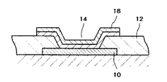
ビルドアップ法は、下層の銅などからなる配線パターン10上に絶縁層12を塗布または積層して形成し(図13)、この絶縁層12にビアホール14をレーザー加工もしくはフォトリソグラフィーによって形成し(図14)、底面に配線パターン10が露出するビアホール14内および絶縁層12上に無電解銅めっき、次いで電解銅めっきを施して、絶縁層12上に銅めっき層16を形成し(図15)、この銅めっき層16をエッチング加工して上層の配線パターン18を形成する(図16)ものである。この工程を繰り返すことによって、下層の配線パターン10と上層の配線パターン18とがビアめっき皮膜を介して電気的に接続される多層の回路基板が製造される。
【0003】
ところで、絶縁層12を形成する場合、ビアホール14内を導電ペーストや絶縁樹脂で埋めて、ビアホール14に起因する絶縁層表面の段差を解消するようにしているが、工数が多くなるだけでなく、平坦化にも限界がある。
そこで、昨今、ビアホール内を銅めっきで埋めるビアフィリングめっき方法が提案されている。
このビアフィリングめっき方法では、めっき液の攪拌に工夫をこらし、ビアホール内にもめっき液が良好に回り込むようにするとか、めっき液にめっき促進剤を添加し、ビアホール内のめっきの付きまわりを良好にするとかして、ビアホール内が銅めっきで埋まるようにしている。
【0004】
【発明が解決しようとする課題】
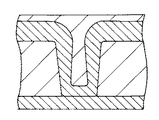
しかしながら、昨今では、配線パターンがますますファイン化し、そのためにビアホールも小径化し、アスペクト比の大きなものとなっていることから、ビアホールを銅めっきで埋めることは困難になっている。
特に、めっき電流はコーナー部に集中しやすいことから、ビアホールの開口縁部にめっきが厚く付き、図17に示すようにビアホールが袋穴状となり、この袋穴内にめっき液が残留するなどの課題が生じている。
【0005】
そこで、本発明は上記課題を解決すべくなされたものであり、その目的とするところは、アスペクト比の大きな小径のビアホール内も良好に銅めっきで埋めることができるビアフィリングめっき方法を提供するにある。
【0006】
【課題を解決するための手段】
本発明は上記目的を達成するため次の構成を備える。
すなわち、導体層が底面に露出するように基板の絶縁層に形成されたビアホール内に、銅めっきを施してビアホール内をめっき金属により充填するビアフィリングめっき方法において、前記基板の絶縁層表面およびビアホールの底面を含む壁面に銅皮膜を形成する銅皮膜形成工程と、めっき促進剤が添加された水溶液中に、前記銅皮膜が形成された基板を浸漬して、前記銅皮膜表面にめっき促進剤を付着させる浸漬工程と、ビアホールの底面を含む内壁面を除く前記銅皮膜表面に付着しためっき促進剤を除去する剥離工程と、前記剥離工程の後、絶縁層表面に形成された銅皮膜およびビアホールの底面を含む壁面に形成された銅皮膜上に電解銅めっきを施して前記ビアホール内にめっき金属を充填する電解銅めっき工程とを含むことを特徴としている。
【0007】
上記方法によれば、ビアホール内に確実にめっき促進剤を付着させて基板の絶縁層表面との間にめっき条件の差異をつけることができ、ビアホール内にも電流を集中させることができ、アスペクト比の大きなビアホールであっても十分に銅めっきで埋めることができる。
【0008】
めっき促進剤として、下記の一般式〔化3〕もしくは〔化4〕で表される1種以上の硫黄化合物を用いることができる。これら硫黄化合物は、濡れ性を向上させるための、ポリエチレングリコールやポリプロピレングリコールなどの非イオン界面活性剤を添加した水溶液として用いる。
【化3】
【0009】
前記剥離工程は、銅のエッチング液を用いるエッチング処理、シアン電解浴を用いるシアン電解処理、前記銅皮膜表面に紫外線を斜めに照射する紫外線処理、または前記銅皮膜表面を研磨する研磨処理などで行うことができる。
【0010】
前記剥離工程を省き、前記浸漬工程の後、前記電解銅めっき工程の初期の段階において、逆電解処理を行ってもよい。
また、前記剥離工程を省き、前記浸漬工程の後、前記電解銅めっき工程において正負の反転するパルスめっきを行ってもよい。
【0011】
また、前記電解銅めっき工程において、めっき促進剤を含まない電解銅めっき液を用いると好適である。
さらに、前記めっき促進剤に3−メルカプト−1−プロパンスルホン酸ナトリウムもしくは2−メルカプトエタンスルホン酸ナトリウムを用いて前記浸漬工程を行い、前記剥離工程を省き、前記電解銅めっき工程において、めっき促進剤を含まない電解銅めっき液を用いるようにしてもよい。
また、前記浸漬工程の前に、前記銅皮膜表面に銅ストライクめっきを施すようにすると好適である。
【0012】
【発明の実施の形態】
以下、本発明の好適な実施の形態を添付図面に基づいて詳細に説明する。
まず、図1に示すように、下層の導体層となる配線パターン10が形成された基板上に、絶縁層12を塗布または積層して形成し、絶縁層12にレーザー加工もしくはフォトリソグラフィーにより底面に配線パターン10が露出するビアホール14を形成する。例えば、基板上に、ポリフェニレンエーテル(PPE)の樹脂シートを加熱加圧して積層することにより絶縁層を形成し、この絶縁層にYAGレーザー、炭酸ガスレーザー等によるレーザー加工によりビアホールを形成するのである。
次に、無電解銅めっきを施して、絶縁層12およびビアホール14内に無電解銅めっき皮膜21を形成する。なお、無電解銅めっきに代えて、スパッタリングや蒸着によって銅皮膜21を形成してもよい。以下では、無電解銅めっき皮膜で説明する。
【0013】
次に上記基板20を、めっき促進剤が添加された水溶液中に浸漬し、無電解銅めっき皮膜21上にめっき促進剤22を付着させる(めっき促進剤層22、図2)。
めっき促進剤としては、3−メルカプト−1−プロパンスルホン酸ナトリウムもしくは2−メルカプトエタンスルホン酸ナトリウム等の、一般式
【化5】
【化6】
【0014】
これらめっき促進剤は、ブライトナー(光沢剤)と呼ばれる銅めっき液に添加する添加物の一種でもある。
めっき促進剤が被めっき物表面に付着すると、抵抗値が低下し、電流が集中してめっきが促進されると考えられる。
本発明におけるめっき促進剤とは、銅めっき液に添加した場合に、添加しない場合に比して、めっき液中に設置した参照電極に対する陰極電位が、正側に移動する硫黄化合物と定義する。
上記めっき促進剤を1種、もしくは2種以上を混合して用いる。
このめっき促進剤の水溶液の濃度は特に限定されないが、数ppm〜数%の濃度で用いることができる。
また、水溶液にかびなどが繁殖しないように、硫酸、硫酸銅などの酸性成分を添加するようにしてもよい。
【0015】
めっき促進剤溶液は常温で用い、基板20の浸漬時間はめっき促進剤溶液の濃度にもよるが、概ね5分〜15分程度と比較的長時間浸漬し、ビアホール14内へ十分にめっき促進剤溶液が進入するようにするとよい。まためっき促進剤溶液を攪拌するか、基板20を揺動させるようにするとよい。
なお、めっき促進剤溶液の基板20への濡れ性を向上させるため、基板20をあらかじめ界面活性剤溶液等の前処理液に浸漬するとよい。
浸漬後、基板20を適宜水洗する。水洗してもめっき促進剤が落ちてしまうことはない。
【0016】
次に、図3に示すように、ビアホール14内を除く絶縁層12表面の無電解銅めっき皮膜21表面に付着しためっき促進剤22を剥離する。
この剥離工程は、塩化第1鉄水溶液等の銅のエッチング液に基板20を浸漬することで行える。基板20をこのエッチング液に浸漬し、直ちに水洗するようにする。銅のエッチング液に基板20を短時間浸漬した場合には、ビアホール14内にまでエッチング液が入り込まないので、ビアホール14内を除く無電解銅めっき皮膜21上のめっき促進剤22を選択的に剥離することができる。
【0017】
上記剥離工程は、シアン電解浴によるシアン電解処理によっても行うことができる。あるいは
無電解銅めっき21表面に対して紫外線を斜めに照射する紫外線処理によってめっき促進剤22を分解させて剥離するようにしてもよい。紫外線を基板20に対して斜めに照射することによって、紫外線がビアホール14内に進入せず、したがって、ビアホール14以外の部分に付着しているめっき促進剤を選択的に剥離可能である。あるいは、絶縁層12表面の無電解銅めっき皮膜21表面を研磨する研磨処理によってもめっき促進剤22を選択的に除去できる。
【0018】
このような剥離工程を行って後、絶縁層12表面およびビアホール14内の無電解銅めっき皮膜21上に電解銅めっきを施してビアフィリングを行う電解銅めっき工程を行う。
銅めっき液の組成の一例を下記に示す。
硫酸銅 120g/l
硫酸 190g/l
塩素イオン 50ppm
添加剤 40ml/l
添加剤の組成の一例を下記に示す。
PEG4000 180g/l
(ポリエチレングリコール)
PPG425 72g/l
(ポリプロピレングリコール)
添加剤としてこのようなポリマー成分を添加するとよい。
【0019】
上記銅めっき液には、めっき促進剤が混入されていない。
銅めっき液の組成は上記に限定されるものではない。
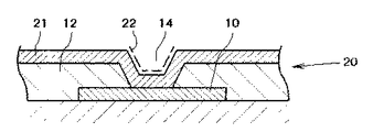
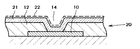
上記のように、めっき促進剤溶液に基板20を浸漬した後、ビアホール14内を除く絶縁層表面に付着しためっき促進剤を剥離して電解銅めっきを行うことによって、図6に示すように、ビアホール14内に電流が集中し、ビアホール14内を電解銅めっきで埋めるビアフィリングが行える(図4)。
次に、絶縁層12上に形成された銅めっき皮膜23および21をエッチングして上層の配線パターン24を形成する(図5)。
上記工程を繰り返すことによって、層間の配線パターンが銅めっきによって導通された多層の回路基板を得ることができる。
【0020】
図12は、めっき促進剤の特性を示すグラフである。
上記銅めっき液に、めっき促進剤を添加しないで銅めっきを行った場合と、5分後にめっき促進剤を銅めっき液に1ppm添加した場合における、銅めっき液中に設置した参照電極に対する陰極電位の変移を調べたものである。めっき促進剤として、3−メルカプト−1−プロパンスルホン酸ナトリウム、2−メルカプトエタンスルホン酸ナトリウム、ビス−(3−スルフォプロピル)−ジスルファイドジソディウムを添加した場合のいずれも、添加前に比して陰極電位が正側にシフトしていることがわかる。
【0021】
なお、電解銅めっき液には、ビアホール14内に効果的に電流が集中するように、めっき促進剤を添加しないものを用いるのが好適であるが、めっき促進剤を添加した電解銅めっき液を用いてもよい。この場合にも、既に上記浸漬工程でビアホール14内にはめっき促進剤が付着しているため、ビアホール14内に電流が集中し、ビアホール14内を銅めっきで埋めることができる。
【0022】
また、前記剥離工程の代わりに、電解銅めっき工程の初期の段階で、逆電解処理を行うようにしてもよい。例えば、電解銅めっき開始後数分後に、30秒毎等に陽極(正)と陰極(負)の極性を反転させて数分間銅めっきを行う。極性を反転した際に、ビアホール14以外の部分に付着しているめっき促進剤の剥離が進行し、ビアホール14内へ電流を集中させることができ、ビアホール14内を銅めっきで埋めることができた。
【0023】
あるいは、前記剥離工程の代わりに、電解銅めっき工程で正負の反転するパルスめっきを行うようにしてもよい。例えば、正電流(めっき電流)を10ms、負電流を1msとするパルスめっき(PPR電解めっき)を行うことにより、ビアホール14以外の部分に付着しているめっき促進剤の剥離作用がなされ、ビアホール14内を銅めっきで埋めることができた。
【0024】
あるいはまた、前記めっき促進剤の剥離工程を省き、電解銅めっきの工程で、めっき促進剤を含まない銅めっき液を用いることだけでもビアホール14内を銅めっきで埋めることができる。
この場合にも既に浸漬処理の段階でビアホール14内にめっき促進剤を付着させてあるので、ビアホール14内に電流を集中できるからである。
【0025】
また、無電解銅めっき工程と浸漬工程との間に、無電解銅めっき皮膜21上に電解によるストライク銅めっき皮膜を形成するめっき工程を行うとさらに好適である。
これにより無電解銅めっき皮膜21上に純粋な銅の皮膜が形成された状態となるので、無電解銅めっき皮膜21の表面の酸化等によるめっき促進剤の未着を防止することができ、この清浄な銅表面にめっき促進剤がムラなく均一に付着するので、確実にビアホール14内を銅めっきで埋めることができるようになる。
【0026】
【実施例】
〔実施例1〕
導体層が底面に露出するように絶縁層にビアホールが形成された基板表面に無電解銅めっきを施し、この基板を、3−メルカプト−1−プロパンスルホン酸ナトリウム(めっき促進剤)の1%水溶液に、15分間揺動させながら浸漬し、無電解銅めっき皮膜の表面にめっき促進剤を付着させた。
水洗後、シアン電解浴(NaCN 20g/l、NaOH 140g/l)で、基板側を陰極にして、常温、1.4V、30秒間電解して、ビアホール内以外の無電解銅めっき皮膜表面のめっき促進剤を剥離した。
水洗後、上記電解銅めっき浴を用いて、常温、1A/dm2の電流密度、100分間のめっき条件で電解銅めっきを施した結果を図7および図8に示す。
図7は開口部の直径46μm、深さ53μm、アスペクト比1.15のビアホールであるが、銅めっきでビアホール−内が完全に埋められている。図8は開口部の直径28μm、深さ53μm、アスペクト比1.89のビアホールであるが、銅めっきでビアホール内が完全に埋められている。
なお、3−メルカプト−1−プロパンスルホン酸ナトリウムの代わりに、2−メルカプトエタンスルホン酸ナトリウムあるいはビス−(3−スルフォプロピル)−ジスルファイドジソディウムを用いた場合にも同様の結果が得られた。また、これら促進剤の1種以上を混合して用いた場合も同様の結果が得られた。
【0027】
〔実施例2〕
導体層が底面に露出するように絶縁層にビアホールが形成された基板表面に無電解銅めっきを施し、この基板を、3−メルカプト−1−プロパンスルホン酸ナトリウム 1.5g/lのめっき促進剤溶液に3分浸漬して、無電解銅めっき皮膜上にめっき促進剤を付着させた。
水洗後、上記電解銅めっきを用いて、常温、1A/dm2の電流密度、100分間のめっき条件で電解銅めっきを施した。その際、めっき開始後2分から9分の間、30秒毎に陽極と陰極の極性を反転させる処理を行った。その結果を図9、図10に示す。
図9は開口部の直径が40μmのビアホールのもの、図10は開口部の直径が60μmのビアホールのものであるが、いずれもビアホール内が十分に銅めっきで埋められている。
なお、3−メルカプト−1−プロパンスルホン酸ナトリウムの代わりに、2−メルカプトエタンスルホン酸ナトリウムあるいはビス−(3−スルフォプロピル)−ジスルファイドジソディウムを用いた場合にも同様の結果が得られた。また、これら促進剤の1種以上を混合して用いた場合も同様の結果が得られた。
【0028】
〔実施例3〕
導体層が底面に露出するように絶縁層にビアホールが形成された基板表面に無電解銅めっきを施し、この基板を、3−メルカプト−1−プロパンスルホン酸ナトリウムの1%水溶液に、10分間揺動させながら浸漬し、無電解銅めっき皮膜の表面にめっき促進剤を付着させた。
水洗後、実施例1の電解銅めっき液を用いて、下記の条件でPPR電解銅めっきを行った。
正電流時間 10ms
負電流時間 0.5ms
正電流密度 1A/dm2
負電流密度 3A/dm2
めっき時間100分
上記電解銅めっきの結果を図11に示す。開口部の直径が100μm、深さ30μmのビアホール内を十分に銅めっきで埋めることができた。
なお、3−メルカプト−1−プロパンスルホン酸ナトリウムの代わりに、2−メルカプトエタンスルホン酸ナトリウムあるいはビス−(3−スルフォプロピル)−ジスルファイドジソディウムを用いた場合にも同様の結果が得られた。また、これら促進剤の1種以上を混合して用いた場合も同様の結果が得られた。
【0029】
以上本発明につき好適な実施例を挙げて種々説明したが、本発明はこの実施例に限定されるものではなく、発明の精神を逸脱しない範囲内で多くの改変を施し得るのはもちろんである。
【0030】
【発明の効果】
以上のように本発明によれば、アスペクト比の大きなビアホールであっても十分にビアフィリングを行えるという著効を奏する。
【図面の簡単な説明】
【図1】銅皮膜を形成した状態の説明図、
【図2】めっき促進剤溶液に浸漬した状態の説明図、
【図3】めっき促進剤を部分剥離した状態の説明図、
【図4】ビアフィリングをした状態の説明図、
【図5】上層の配線パターンを形成した説明図、
【図6】ビアホールに電流が集中した状態を示す説明図、
【図7】実施例1のビアフィリング状態を示す説明図、
【図8】実施例1のビアフィリング状態を示す説明図、
【図9】実施例2のビアフィリング状態を示す説明図、
【図10】実施例2のビアフィリング状態を示す説明図、
【図11】実施例3のビアフィリング状態を示す説明図、
【図12】めっき促進剤の特性を示すグラフである。
【図13】ビルドアップ法の工程を示し、絶縁層を形成した説明図、
【図14】ビアホールを形成した説明図、
【図15】銅めっき皮膜を形成した説明図、
【図16】配線パターンを形成した説明図、
【図17】ビアホールが袋穴状になった状態の説明図である。
【符号の説明】
10 配線パターン
12 絶縁層
14 ビアホール
20 基板
21 無電解銅めっき皮膜
22 めっき促進剤(層)
23 銅めっき皮膜
24 配線パターン[0001]
TECHNICAL FIELD OF THE INVENTION
The present invention relates to a via filling plating method.
[0002]
[Prior art]
There is a so-called build-up method as a method for manufacturing a multilayer circuit board on which electronic components such as semiconductor chips are mounted.
In the build-up method, an
[0003]
By the way, when the
Therefore, a via filling plating method for filling the via holes with copper plating has recently been proposed.
In this via filling plating method, a method of stirring the plating solution is devised so that the plating solution can satisfactorily flow into the via hole, or a plating accelerator is added to the plating solution to improve the plating coverage in the via hole. In other words, the inside of the via hole is filled with copper plating.
[0004]
[Problems to be solved by the invention]
However, recently, wiring patterns have become finer and finer, and the via holes have been reduced in diameter and the aspect ratio has been increased. Therefore, it is difficult to fill the via holes with copper plating.
In particular, since the plating current tends to concentrate on the corners, the plating is thickly attached to the opening edge of the via hole, and the via hole becomes a blind hole as shown in FIG. 17, and the plating solution remains in the blind hole. Has occurred.
[0005]
Therefore, the present invention has been made to solve the above-described problems, and an object of the present invention is to provide a via filling plating method capable of well filling a small-diameter via hole having a large aspect ratio with copper plating. is there.
[0006]
[Means for Solving the Problems]
The present invention has the following configuration to achieve the above object.
That is, in a via-filling plating method of performing copper plating in a via hole formed in an insulating layer of a substrate so that a conductive layer is exposed on a bottom surface and filling the via hole with a plating metal, the insulating layer surface of the substrate and the via hole A copper film forming step of forming a copper film on a wall surface including the bottom surface of the substrate, and immersing the substrate on which the copper film is formed in an aqueous solution to which a plating accelerator has been added, so that a plating accelerator is applied to the surface of the copper film. An immersion step of adhering, a stripping step of removing a plating accelerator adhering to the surface of the copper film excluding an inner wall surface including a bottom surface of the via hole, and a step of removing the copper film and the via hole formed on the insulating layer surface after the stripping step. Electrolytic copper plating step of applying electrolytic copper plating on a copper film formed on a wall surface including a bottom surface and filling a plating metal in the via hole. To have.
[0007]
According to the above method, a plating accelerator can be securely attached to the via hole to make a difference in plating conditions between the substrate and the insulating layer surface, and current can be concentrated also in the via hole. Even a via hole having a large ratio can be sufficiently filled with copper plating.
[0008]
One or more sulfur compounds represented by the following general formula [Chemical formula 3] or [Chemical formula 4] can be used as the plating accelerator. These sulfur compounds are used as an aqueous solution to which a nonionic surfactant such as polyethylene glycol or polypropylene glycol for improving the wettability is added.
Embedded image
[0009]
The stripping step is performed by an etching process using a copper etchant, a cyan electrolytic process using a cyan electrolytic bath, an ultraviolet process for obliquely irradiating the copper film surface with ultraviolet light, a polishing process for polishing the copper film surface, or the like. be able to.
[0010]
The stripping step may be omitted, and after the dipping step, a reverse electrolytic treatment may be performed in an initial stage of the electrolytic copper plating step.
Further, the peeling step may be omitted, and after the dipping step, pulse plating in which the polarity is reversed may be performed in the electrolytic copper plating step.
[0011]
In the electrolytic copper plating step, it is preferable to use an electrolytic copper plating solution containing no plating accelerator.
Further, the immersion step is performed using sodium 3-mercapto-1-propanesulfonate or sodium 2-mercaptoethanesulfonate as the plating accelerator, the stripping step is omitted, and in the electrolytic copper plating step, a plating accelerator is used. May be used.
Further, it is preferable that a copper strike plating is applied to the surface of the copper film before the dipping step.
[0012]
BEST MODE FOR CARRYING OUT THE INVENTION
Hereinafter, preferred embodiments of the present invention will be described in detail with reference to the accompanying drawings.
First, as shown in FIG. 1, an
Next, an electroless
[0013]
Next, the
As the plating accelerator, a general formula such as sodium 3-mercapto-1-propanesulfonate or sodium 2-mercaptoethanesulfonate is used.
[0014]
These plating accelerators are also a kind of additive added to a copper plating solution called a brightener (brightener).
It is considered that when the plating accelerator adheres to the surface of the object to be plated, the resistance value decreases, the current is concentrated, and the plating is promoted.
The plating accelerator in the present invention is defined as a sulfur compound in which, when added to a copper plating solution, the cathode potential with respect to a reference electrode provided in the plating solution moves to the positive side as compared with the case where it is not added.
One of the above plating accelerators or a mixture of two or more thereof is used.
Although the concentration of the aqueous solution of the plating accelerator is not particularly limited, it can be used at a concentration of several ppm to several%.
Further, an acidic component such as sulfuric acid or copper sulfate may be added so that mold and the like do not propagate in the aqueous solution.
[0015]
The plating accelerator solution is used at room temperature, and the immersion time of the
In order to improve the wettability of the plating accelerator solution to the
After the immersion, the
[0016]
Next, as shown in FIG. 3, the plating
This peeling step can be performed by immersing the
[0017]
The peeling step can also be performed by cyan electrolytic treatment using a cyan electrolytic bath. Alternatively, the plating
[0018]
After performing such a peeling step, an electrolytic copper plating step of performing electrolytic via plating on the surface of the insulating
An example of the composition of the copper plating solution is shown below.
Copper sulfate 120g / l
Sulfuric acid 190g / l
Chloride ion 50ppm
Additive 40ml / l
An example of the composition of the additive is shown below.
PEG4000 180g / l
(Polyethylene glycol)
PPG425 72g / l
(Polypropylene glycol)
It is preferable to add such a polymer component as an additive.
[0019]
The copper plating solution does not contain a plating accelerator.
The composition of the copper plating solution is not limited to the above.
As described above, after immersing the
Next, the
By repeating the above steps, it is possible to obtain a multilayer circuit board in which the wiring patterns between the layers are conducted by copper plating.
[0020]
FIG. 12 is a graph showing the characteristics of the plating accelerator.
Cathode potential with respect to the reference electrode installed in the copper plating solution when copper plating was performed without adding a plating accelerator to the copper plating solution, and when 1 ppm of the plating accelerator was added to the copper plating solution after 5 minutes. This is a study of the transition. Prior to the addition of any of sodium 3-mercapto-1-propanesulfonate, sodium 2-mercaptoethanesulfonate, and bis- (3-sulfopropyl) -disulfide disodium as a plating accelerator, In comparison, it can be seen that the cathode potential has shifted to the positive side.
[0021]
It is preferable to use an electrolytic copper plating solution to which a plating accelerator is not added so that the current is effectively concentrated in the via
[0022]
Further, instead of the peeling step, a reverse electrolytic treatment may be performed at an early stage of the electrolytic copper plating step. For example, several minutes after the start of electrolytic copper plating, the polarity of the anode (positive) and the polarity of the cathode (negative) are reversed every 30 seconds or the like, and copper plating is performed for several minutes. When the polarity was reversed, the plating accelerator adhering to portions other than the via
[0023]
Alternatively, pulse plating in which the polarity is reversed in the electrolytic copper plating step may be performed instead of the peeling step. For example, by performing pulse plating (PPR electrolytic plating) with a positive current (plating current) of 10 ms and a negative current of 1 ms, a plating accelerator adhering to portions other than the via holes 14 is separated, and the via holes 14 are removed. The inside could be filled with copper plating.
[0024]
Alternatively, the via
Also in this case, since the plating accelerator has already been deposited in the via
[0025]
It is more preferable to perform a plating step of forming a strike copper plating film on the electroless
As a result, a pure copper film is formed on the electroless
[0026]
【Example】
[Example 1]
Electroless copper plating is applied to the surface of the substrate on which the via hole is formed in the insulating layer so that the conductor layer is exposed at the bottom, and this substrate is treated with a 1% aqueous solution of sodium 3-mercapto-1-propanesulfonate (plating accelerator). For 15 minutes while oscillating, so that a plating accelerator was attached to the surface of the electroless copper plating film.
After washing with water, electrolysis is carried out in a cyan electrolytic bath (NaCN 20 g / l, NaOH 140 g / l) with the substrate side as a cathode at room temperature and 1.4 V for 30 seconds, and plating of the surface of the electroless copper plating film other than in the via hole The accelerator was stripped.
After washing with water, by using the electrolytic copper plating bath, a normal temperature, a current density of 1A /
FIG. 7 shows a via hole having an opening diameter of 46 μm, a depth of 53 μm, and an aspect ratio of 1.15. The via hole is completely filled with copper plating. FIG. 8 shows a via hole having an opening diameter of 28 μm, a depth of 53 μm, and an aspect ratio of 1.89. The via hole is completely filled with copper plating.
Similar results are obtained when sodium 2-mercaptoethanesulfonate or bis- (3-sulfopropyl) -disulfide disodium is used instead of sodium 3-mercapto-1-propanesulfonate. Was done. Similar results were obtained when one or more of these accelerators were used in combination.
[0027]
[Example 2]
Electroless copper plating is applied to the surface of the substrate on which the via hole is formed in the insulating layer so that the conductive layer is exposed on the bottom surface, and the substrate is plated with 1.5 g / l of a plating accelerator of sodium 3-mercapto-1-propanesulfonate. It was immersed in the solution for 3 minutes to attach a plating accelerator on the electroless copper plating film.
After washing with water, electrolytic copper plating was performed using the above-described electrolytic copper plating at room temperature, a current density of 1 A / dm 2 , and plating conditions for 100 minutes. At that time, a process of inverting the polarity of the anode and the cathode was performed every 30 seconds for 2 to 9 minutes after the plating was started. The results are shown in FIGS.
9 shows a via hole having a diameter of 40 μm in the opening, and FIG. 10 shows a via hole having a diameter of 60 μm in the opening. In each case, the inside of the via hole is sufficiently filled with copper plating.
Similar results are obtained when sodium 2-mercaptoethanesulfonate or bis- (3-sulfopropyl) -disulfide disodium is used instead of sodium 3-mercapto-1-propanesulfonate. Was done. Similar results were obtained when one or more of these accelerators were used in combination.
[0028]
[Example 3]
Electroless copper plating is applied to the surface of the substrate on which the via hole is formed in the insulating layer so that the conductive layer is exposed at the bottom, and this substrate is shaken for 10 minutes in a 1% aqueous solution of sodium 3-mercapto-1-propanesulfonate. The plating accelerator was attached to the surface of the electroless copper plating film while moving.
After water washing, PPR electrolytic copper plating was performed using the electrolytic copper plating solution of Example 1 under the following conditions.
Positive current time 10ms
Negative current time 0.5ms
Positive current density 1A / dm 2
Negative current density 3A / dm 2
FIG. 11 shows the results of the above electrolytic copper plating for a plating time of 100 minutes. The inside of the via hole having an opening diameter of 100 μm and a depth of 30 μm was sufficiently filled with copper plating.
Similar results are obtained when sodium 2-mercaptoethanesulfonate or bis- (3-sulfopropyl) -disulfide disodium is used instead of sodium 3-mercapto-1-propanesulfonate. Was done. Similar results were obtained when one or more of these accelerators were used in combination.
[0029]
Although the present invention has been described in detail with reference to preferred embodiments, the present invention is not limited to the embodiments, and it is needless to say that many modifications can be made without departing from the spirit of the invention. .
[0030]
【The invention's effect】
As described above, according to the present invention, there is a significant effect that via filling can be sufficiently performed even in a via hole having a large aspect ratio.
[Brief description of the drawings]
FIG. 1 is an explanatory view of a state where a copper film is formed,
FIG. 2 is an explanatory view of a state of being immersed in a plating accelerator solution,
FIG. 3 is an explanatory view showing a state where a plating accelerator is partially peeled off,
FIG. 4 is an explanatory view showing a state in which via filling is performed;
FIG. 5 is an explanatory diagram in which an upper wiring pattern is formed,
FIG. 6 is an explanatory view showing a state in which current is concentrated in a via hole;
FIG. 7 is an explanatory view showing a via filling state according to the first embodiment;
FIG. 8 is an explanatory view showing a via filling state according to the first embodiment;
FIG. 9 is an explanatory view showing a via filling state according to the second embodiment;
FIG. 10 is an explanatory view showing a via filling state according to the second embodiment;
FIG. 11 is an explanatory view showing a via-filling state according to the third embodiment;
FIG. 12 is a graph showing characteristics of a plating accelerator.
FIG. 13 is an explanatory view showing a step of a build-up method and forming an insulating layer;
FIG. 14 is an explanatory view in which a via hole is formed,
FIG. 15 is an explanatory view in which a copper plating film is formed,
FIG. 16 is an explanatory view in which a wiring pattern is formed,
FIG. 17 is an explanatory diagram of a state in which a via hole has a blind hole shape.
[Explanation of symbols]
23
Claims (10)
前記基板の絶縁層表面およびビアホールの底面を含む壁面に銅皮膜を形成する銅皮膜形成工程と、
めっき促進剤が添加された水溶液中に、前記銅皮膜が形成された基板を浸漬して、前記銅皮膜表面にめっき促進剤を付着させる浸漬工程と、
ビアホールの底面を含む内壁面を除く前記銅皮膜表面に付着しためっき促進剤を除去する剥離工程と、
前記剥離工程の後、絶縁層表面に形成された銅皮膜およびビアホールの底面を含む壁面に形成された銅皮膜上に電解銅めっきを施して前記ビアホール内にめっき金属を充填する電解銅めっき工程とを含むことを特徴とするビアフィリングめっき方法。In a via filling plating method in which a via hole formed in an insulating layer of a substrate such that a conductive layer is exposed on a bottom surface is subjected to copper plating and the inside of the via hole is filled with a plating metal,
A copper film forming step of forming a copper film on the insulating layer surface of the substrate and the wall surface including the bottom surface of the via hole,
An immersion step of immersing the substrate on which the copper film is formed in an aqueous solution to which a plating accelerator has been added, and attaching a plating accelerator to the surface of the copper film,
A peeling step of removing a plating accelerator attached to the copper film surface excluding an inner wall surface including a bottom surface of a via hole,
After the peeling step, an electrolytic copper plating step of performing electrolytic copper plating on the copper film formed on the insulating layer surface and the copper film formed on the wall surface including the bottom surface of the via hole and filling the via hole with a plating metal, A via-filling plating method comprising:
前記剥離工程を省き、
前記電解銅めっき工程において、めっき促進剤を含まない電解銅めっき液を用いることを特徴とする請求項1記載のビアフィリングめっき方法。Performing the immersion step using sodium 3-mercapto-1-propanesulfonate or sodium 2-mercaptoethanesulfonate as the plating accelerator;
Omit the peeling step,
The via-filling plating method according to claim 1, wherein in the electrolytic copper plating step, an electrolytic copper plating solution containing no plating accelerator is used.
Priority Applications (6)
| Application Number | Priority Date | Filing Date | Title |
|---|---|---|---|
| JP2000334044A JP3594894B2 (en) | 2000-02-01 | 2000-11-01 | Via filling plating method |
| US09/772,457 US6755957B2 (en) | 2000-02-01 | 2001-01-30 | Method of plating for filling via holes |
| EP01300837A EP1122989B1 (en) | 2000-02-01 | 2001-01-31 | Method of plating for filling via holes |
| TW90101961A TW574438B (en) | 2000-02-01 | 2001-01-31 | Method of plating for filling via holes |
| KR20010004601A KR100730326B1 (en) | 2000-02-01 | 2001-01-31 | Plating method to fill the empty hole |
| DE60126853T DE60126853T2 (en) | 2000-02-01 | 2001-01-31 | Plating method for filling contact holes |
Applications Claiming Priority (3)
| Application Number | Priority Date | Filing Date | Title |
|---|---|---|---|
| JP2000023794 | 2000-02-01 | ||
| JP2000-23794 | 2000-02-01 | ||
| JP2000334044A JP3594894B2 (en) | 2000-02-01 | 2000-11-01 | Via filling plating method |
Publications (2)
| Publication Number | Publication Date |
|---|---|
| JP2001291954A JP2001291954A (en) | 2001-10-19 |
| JP3594894B2 true JP3594894B2 (en) | 2004-12-02 |
Family
ID=26584623
Family Applications (1)
| Application Number | Title | Priority Date | Filing Date |
|---|---|---|---|
| JP2000334044A Expired - Fee Related JP3594894B2 (en) | 2000-02-01 | 2000-11-01 | Via filling plating method |
Country Status (6)
| Country | Link |
|---|---|
| US (1) | US6755957B2 (en) |
| EP (1) | EP1122989B1 (en) |
| JP (1) | JP3594894B2 (en) |
| KR (1) | KR100730326B1 (en) |
| DE (1) | DE60126853T2 (en) |
| TW (1) | TW574438B (en) |
Families Citing this family (53)
| Publication number | Priority date | Publication date | Assignee | Title |
|---|---|---|---|---|
| US7449098B1 (en) | 1999-10-05 | 2008-11-11 | Novellus Systems, Inc. | Method for planar electroplating |
| US7531079B1 (en) | 1998-10-26 | 2009-05-12 | Novellus Systems, Inc. | Method and apparatus for uniform electropolishing of damascene IC structures by selective agitation |
| US6534116B2 (en) | 2000-08-10 | 2003-03-18 | Nutool, Inc. | Plating method and apparatus that creates a differential between additive disposed on a top surface and a cavity surface of a workpiece using an external influence |
| US6491806B1 (en) | 2000-04-27 | 2002-12-10 | Intel Corporation | Electroplating bath composition |
| WO2002015245A2 (en) * | 2000-08-10 | 2002-02-21 | Nutool, Inc. | Plating method and apparatus that creates a differential between additive disposed on a top surface and a cavity surface of a workpiece using an external influence |
| US6921551B2 (en) * | 2000-08-10 | 2005-07-26 | Asm Nutool, Inc. | Plating method and apparatus for controlling deposition on predetermined portions of a workpiece |
| US6858121B2 (en) * | 2000-08-10 | 2005-02-22 | Nutool, Inc. | Method and apparatus for filling low aspect ratio cavities with conductive material at high rate |
| US6863795B2 (en) * | 2001-03-23 | 2005-03-08 | Interuniversitair Microelektronica Centrum (Imec) | Multi-step method for metal deposition |
| JP4000796B2 (en) * | 2001-08-08 | 2007-10-31 | 株式会社豊田自動織機 | Via hole copper plating method |
| CN1283848C (en) * | 2001-10-16 | 2006-11-08 | 新光电气工业株式会社 | Method of copper-plating small-diameter holes |
| JP2003168860A (en) * | 2001-11-30 | 2003-06-13 | Cmk Corp | Printed wiring board and method of manufacturing the same |
| JP3976564B2 (en) * | 2001-12-20 | 2007-09-19 | 日本リーロナール有限会社 | Via filling method |
| JP3964263B2 (en) * | 2002-05-17 | 2007-08-22 | 株式会社デンソー | Blind via hole filling method and through electrode forming method |
| US7405163B1 (en) * | 2003-12-17 | 2008-07-29 | Novellus Systems, Inc. | Selectively accelerated plating of metal features |
| US7449099B1 (en) * | 2004-04-13 | 2008-11-11 | Novellus Systems, Inc. | Selectively accelerated plating of metal features |
| US7799200B1 (en) | 2002-07-29 | 2010-09-21 | Novellus Systems, Inc. | Selective electrochemical accelerator removal |
| JP2004342750A (en) | 2003-05-14 | 2004-12-02 | Toshiba Corp | Electronic device manufacturing method |
| US8530359B2 (en) | 2003-10-20 | 2013-09-10 | Novellus Systems, Inc. | Modulated metal removal using localized wet etching |
| US8158532B2 (en) | 2003-10-20 | 2012-04-17 | Novellus Systems, Inc. | Topography reduction and control by selective accelerator removal |
| DE102004005300A1 (en) * | 2004-01-29 | 2005-09-08 | Atotech Deutschland Gmbh | Process for treating carrier material for the production of powder carriers and application of the process |
| US20050224358A1 (en) * | 2004-03-30 | 2005-10-13 | Lsi Logic Corporation | Method for improved local planarity control during electropolishing |
| JP4150930B2 (en) * | 2004-10-21 | 2008-09-17 | 日立電線株式会社 | Method for manufacturing double-sided wiring tape carrier for semiconductor device |
| CN101189921A (en) * | 2005-06-01 | 2008-05-28 | 松下电器产业株式会社 | Circuit board, manufacturing method thereof, and electronic component using the same |
| US7550070B2 (en) | 2006-02-03 | 2009-06-23 | Novellus Systems, Inc. | Electrode and pad assembly for processing conductive layers |
| JP4759416B2 (en) * | 2006-03-20 | 2011-08-31 | 新光電気工業株式会社 | Non-cyanide electroless gold plating solution and electroless gold plating method |
| US7405154B2 (en) * | 2006-03-24 | 2008-07-29 | International Business Machines Corporation | Structure and method of forming electrodeposited contacts |
| US7575666B2 (en) * | 2006-04-05 | 2009-08-18 | James Watkowski | Process for electrolytically plating copper |
| JP4862508B2 (en) * | 2006-06-12 | 2012-01-25 | 日立電線株式会社 | Conductor pattern forming method |
| US8500985B2 (en) | 2006-07-21 | 2013-08-06 | Novellus Systems, Inc. | Photoresist-free metal deposition |
| US7732329B2 (en) | 2006-08-30 | 2010-06-08 | Ipgrip, Llc | Method and apparatus for workpiece surface modification for selective material deposition |
| US20080148561A1 (en) * | 2006-12-22 | 2008-06-26 | Motorola, Inc. | Methods for making printed wiring boards |
| KR100832705B1 (en) * | 2006-12-23 | 2008-05-28 | 동부일렉트로닉스 주식회사 | Via plating method of system-in-package and its system |
| KR200454218Y1 (en) * | 2008-10-08 | 2011-06-23 | 주식회사강산 | Handrail |
| AT506583B9 (en) | 2008-10-23 | 2009-12-15 | Happy Plating Gmbh | ELECTROCHEMICAL COATING PROCESS |
| US8168540B1 (en) | 2009-12-29 | 2012-05-01 | Novellus Systems, Inc. | Methods and apparatus for depositing copper on tungsten |
| KR101705734B1 (en) | 2011-02-18 | 2017-02-14 | 삼성전자주식회사 | Copper electroplating solution and method of copper electroplating using the same |
| EP2551375A1 (en) * | 2011-07-26 | 2013-01-30 | Atotech Deutschland GmbH | Electroless nickel plating bath composition |
| US20140262801A1 (en) * | 2013-03-14 | 2014-09-18 | Rohm And Haas Electronic Materials Llc | Method of filling through-holes |
| US9598787B2 (en) * | 2013-03-14 | 2017-03-21 | Rohm And Haas Electronic Materials Llc | Method of filling through-holes |
| JP6327463B2 (en) * | 2013-10-09 | 2018-05-23 | 日立化成株式会社 | Manufacturing method of multilayer wiring board |
| JP6350064B2 (en) * | 2013-10-09 | 2018-07-04 | 日立化成株式会社 | Manufacturing method of multilayer wiring board |
| JP6350063B2 (en) * | 2013-10-09 | 2018-07-04 | 日立化成株式会社 | Multilayer wiring board |
| US10154598B2 (en) * | 2014-10-13 | 2018-12-11 | Rohm And Haas Electronic Materials Llc | Filling through-holes |
| JP6625872B2 (en) | 2015-11-25 | 2019-12-25 | 新光電気工業株式会社 | Wiring board and method of manufacturing wiring board |
| US10508357B2 (en) | 2016-02-15 | 2019-12-17 | Rohm And Haas Electronic Materials Llc | Method of filling through-holes to reduce voids and other defects |
| US10512174B2 (en) * | 2016-02-15 | 2019-12-17 | Rohm And Haas Electronic Materials Llc | Method of filling through-holes to reduce voids and other defects |
| JP2017162895A (en) * | 2016-03-08 | 2017-09-14 | 株式会社ジェイデバイス | Wiring structure, printed circuit board, semiconductor device, and manufacturing method of wiring structure |
| EP3826439B1 (en) * | 2019-11-19 | 2026-01-07 | AT & S Austria Technologie & Systemtechnik Aktiengesellschaft | Method of manufacturing a laminated component carrier with blind hole having wedges filled with filling medium by sputtering and back-sputtering |
| KR102254649B1 (en) | 2020-04-14 | 2021-05-24 | 주식회사 디에이피 | Method for electric copper plating of PCB |
| CN113747664B (en) * | 2020-05-29 | 2024-01-05 | 深南电路股份有限公司 | Printed circuit board and manufacturing method thereof |
| CN113795086B (en) * | 2021-10-19 | 2023-04-14 | 重庆新固兴科技有限公司 | Double-sided false sticker machine |
| CN115003032B (en) * | 2022-06-21 | 2023-03-07 | 东莞市国盈电子有限公司 | A motor drive control circuit board and its manufacturing process |
| CN117265530A (en) * | 2023-09-06 | 2023-12-22 | 九江德福科技股份有限公司 | A method to eliminate light transmission points of composite copper foil |
Family Cites Families (11)
| Publication number | Priority date | Publication date | Assignee | Title |
|---|---|---|---|---|
| DE1075398B (en) * | 1954-03-22 | 1960-02-11 | DEHYDAG Deutsche Hydrierwerke G.m.b.H., Düsseldorf | Bath for the galvanic production of metal coatings |
| JPH01143797A (en) * | 1987-11-30 | 1989-06-06 | Mitsumi Electric Co Ltd | Press device |
| US5174886A (en) | 1991-02-22 | 1992-12-29 | Mcgean-Rohco, Inc. | High-throw acid copper plating using inert electrolyte |
| US5252196A (en) | 1991-12-05 | 1993-10-12 | Shipley Company Inc. | Copper electroplating solutions and processes |
| JPH1143797A (en) * | 1997-07-25 | 1999-02-16 | Hideo Honma | Via filling method |
| JPH11298141A (en) * | 1998-04-08 | 1999-10-29 | Hitachi Ltd | Electronic device manufacturing method |
| KR100336829B1 (en) | 1998-04-10 | 2002-05-16 | 모기 쥰이찌 | Fabricating method of multilayered wiring substrate |
| WO1999057342A1 (en) | 1998-04-30 | 1999-11-11 | Ebara Corporation | Method and device for plating substrate |
| US6534116B2 (en) * | 2000-08-10 | 2003-03-18 | Nutool, Inc. | Plating method and apparatus that creates a differential between additive disposed on a top surface and a cavity surface of a workpiece using an external influence |
| JP3124523B2 (en) | 1999-01-28 | 2001-01-15 | 日本エレクトロプレイテイング・エンジニヤース株式会社 | Copper plating method |
| US6224737B1 (en) * | 1999-08-19 | 2001-05-01 | Taiwan Semiconductor Manufacturing Company | Method for improvement of gap filling capability of electrochemical deposition of copper |
-
2000
- 2000-11-01 JP JP2000334044A patent/JP3594894B2/en not_active Expired - Fee Related
-
2001
- 2001-01-30 US US09/772,457 patent/US6755957B2/en not_active Expired - Lifetime
- 2001-01-31 KR KR20010004601A patent/KR100730326B1/en not_active Expired - Lifetime
- 2001-01-31 DE DE60126853T patent/DE60126853T2/en not_active Expired - Lifetime
- 2001-01-31 TW TW90101961A patent/TW574438B/en not_active IP Right Cessation
- 2001-01-31 EP EP01300837A patent/EP1122989B1/en not_active Expired - Lifetime
Also Published As
| Publication number | Publication date |
|---|---|
| KR20010078217A (en) | 2001-08-20 |
| JP2001291954A (en) | 2001-10-19 |
| DE60126853D1 (en) | 2007-04-12 |
| EP1122989B1 (en) | 2007-02-28 |
| KR100730326B1 (en) | 2007-06-19 |
| EP1122989A2 (en) | 2001-08-08 |
| US6755957B2 (en) | 2004-06-29 |
| EP1122989A3 (en) | 2002-07-03 |
| TW574438B (en) | 2004-02-01 |
| US20010013472A1 (en) | 2001-08-16 |
| DE60126853T2 (en) | 2007-08-30 |
Similar Documents
| Publication | Publication Date | Title |
|---|---|---|
| JP3594894B2 (en) | Via filling plating method | |
| JP4248353B2 (en) | Through-hole filling method | |
| JP5828333B2 (en) | Manufacturing method of build-up multilayer substrate | |
| JP5078142B2 (en) | Electrical treatment for filling metal in through holes, especially electrical treatment for filling copper in printed circuit board through holes | |
| JP4195706B2 (en) | Printed wiring board and manufacturing method thereof | |
| JPH04100294A (en) | Manufacture of printed wiring board | |
| US11729917B2 (en) | Method for optimized filling hole and manufacturing fine line on printed circuit board | |
| US7063800B2 (en) | Methods of cleaning copper surfaces in the manufacture of printed circuit boards | |
| CN116076159A (en) | Manufacturing method of printed circuit board | |
| JP4000225B2 (en) | Manufacturing method of multilayer printed wiring board | |
| JPH0362036B2 (en) | ||
| GB2080630A (en) | Printed circuit panels | |
| US4968398A (en) | Process for the electrolytic removal of polyimide resins | |
| JP2858564B2 (en) | Manufacturing method of printed wiring board | |
| JP2006328476A (en) | Plating method | |
| JPH08148810A (en) | Manufacture of printed wiring board | |
| JP2002368380A (en) | Method of manufacturing double-sided flexible circuit board | |
| JPS62230996A (en) | Method for plating aluminum substrate | |
| JP2002076617A (en) | Method for manufacturing printed circuit board and printed circuit board | |
| JP2008088521A (en) | Plating filling method for vias with different depths | |
| JP2004128053A (en) | Manufacturing method of multilayer printed wiring board | |
| JP3191686B2 (en) | Manufacturing method of printed wiring board | |
| JP2006339483A (en) | Wiring board manufacturing method and wiring board | |
| JPH06334337A (en) | Manufacture of printed circuit board | |
| JPH05175652A (en) | Manufacture of printed wiring board |
Legal Events
| Date | Code | Title | Description |
|---|---|---|---|
| TRDD | Decision of grant or rejection written | ||
| A01 | Written decision to grant a patent or to grant a registration (utility model) |
Free format text: JAPANESE INTERMEDIATE CODE: A01 Effective date: 20040824 |
|
| A61 | First payment of annual fees (during grant procedure) |
Free format text: JAPANESE INTERMEDIATE CODE: A61 Effective date: 20040901 |
|
| R150 | Certificate of patent or registration of utility model |
Ref document number: 3594894 Country of ref document: JP Free format text: JAPANESE INTERMEDIATE CODE: R150 Free format text: JAPANESE INTERMEDIATE CODE: R150 |
|
| FPAY | Renewal fee payment (event date is renewal date of database) |
Free format text: PAYMENT UNTIL: 20080910 Year of fee payment: 4 |
|
| FPAY | Renewal fee payment (event date is renewal date of database) |
Free format text: PAYMENT UNTIL: 20080910 Year of fee payment: 4 |
|
| FPAY | Renewal fee payment (event date is renewal date of database) |
Free format text: PAYMENT UNTIL: 20090910 Year of fee payment: 5 |
|
| FPAY | Renewal fee payment (event date is renewal date of database) |
Free format text: PAYMENT UNTIL: 20090910 Year of fee payment: 5 |
|
| FPAY | Renewal fee payment (event date is renewal date of database) |
Free format text: PAYMENT UNTIL: 20100910 Year of fee payment: 6 |
|
| FPAY | Renewal fee payment (event date is renewal date of database) |
Free format text: PAYMENT UNTIL: 20110910 Year of fee payment: 7 |
|
| FPAY | Renewal fee payment (event date is renewal date of database) |
Free format text: PAYMENT UNTIL: 20110910 Year of fee payment: 7 |
|
| FPAY | Renewal fee payment (event date is renewal date of database) |
Free format text: PAYMENT UNTIL: 20120910 Year of fee payment: 8 |
|
| FPAY | Renewal fee payment (event date is renewal date of database) |
Free format text: PAYMENT UNTIL: 20120910 Year of fee payment: 8 |
|
| FPAY | Renewal fee payment (event date is renewal date of database) |
Free format text: PAYMENT UNTIL: 20130910 Year of fee payment: 9 |
|
| LAPS | Cancellation because of no payment of annual fees |