JP3587343B2 - Surface position detection method, exposure apparatus and device manufacturing method - Google Patents
Surface position detection method, exposure apparatus and device manufacturing method Download PDFInfo
- Publication number
- JP3587343B2 JP3587343B2 JP35405297A JP35405297A JP3587343B2 JP 3587343 B2 JP3587343 B2 JP 3587343B2 JP 35405297 A JP35405297 A JP 35405297A JP 35405297 A JP35405297 A JP 35405297A JP 3587343 B2 JP3587343 B2 JP 3587343B2
- Authority
- JP
- Japan
- Prior art keywords
- detection
- exposure apparatus
- surface position
- exposure
- exposed
- Prior art date
- Legal status (The legal status is an assumption and is not a legal conclusion. Google has not performed a legal analysis and makes no representation as to the accuracy of the status listed.)
- Expired - Fee Related
Links
Images


Classifications
-
- G—PHYSICS
- G03—PHOTOGRAPHY; CINEMATOGRAPHY; ANALOGOUS TECHNIQUES USING WAVES OTHER THAN OPTICAL WAVES; ELECTROGRAPHY; HOLOGRAPHY
- G03F—PHOTOMECHANICAL PRODUCTION OF TEXTURED OR PATTERNED SURFACES, e.g. FOR PRINTING, FOR PROCESSING OF SEMICONDUCTOR DEVICES; MATERIALS THEREFOR; ORIGINALS THEREFOR; APPARATUS SPECIALLY ADAPTED THEREFOR
- G03F9/00—Registration or positioning of originals, masks, frames, photographic sheets or textured or patterned surfaces, e.g. automatically
- G03F9/70—Registration or positioning of originals, masks, frames, photographic sheets or textured or patterned surfaces, e.g. automatically for microlithography
- G03F9/7003—Alignment type or strategy, e.g. leveling, global alignment
- G03F9/7023—Aligning or positioning in direction perpendicular to substrate surface
- G03F9/7026—Focusing
-
- G—PHYSICS
- G03—PHOTOGRAPHY; CINEMATOGRAPHY; ANALOGOUS TECHNIQUES USING WAVES OTHER THAN OPTICAL WAVES; ELECTROGRAPHY; HOLOGRAPHY
- G03F—PHOTOMECHANICAL PRODUCTION OF TEXTURED OR PATTERNED SURFACES, e.g. FOR PRINTING, FOR PROCESSING OF SEMICONDUCTOR DEVICES; MATERIALS THEREFOR; ORIGINALS THEREFOR; APPARATUS SPECIALLY ADAPTED THEREFOR
- G03F9/00—Registration or positioning of originals, masks, frames, photographic sheets or textured or patterned surfaces, e.g. automatically
- G03F9/70—Registration or positioning of originals, masks, frames, photographic sheets or textured or patterned surfaces, e.g. automatically for microlithography
- G03F9/7003—Alignment type or strategy, e.g. leveling, global alignment
- G03F9/7046—Strategy, e.g. mark, sensor or wavelength selection
Description
【0001】
【発明の属する技術分野】
本発明は、露光装置の投影光学系光軸方向における基板の被露光領域の面位置を検出する面位置検出技術に関する。
【0002】
【従来の技術】
最近の半導体製造装置、特にステッパと呼ばれる逐次移動型の半導体露光装置に強く求められている性能として生産性の向上がある。すなわちチップメーカはメモリトレンドに沿った集積率の増加に対してチップ代替に見合うメモリコストが提示できるようにチップ単価を抑えて行く必要がある。
露光装置メーカとしては高性能のみならず生産性向上に寄与できるような装置を提供しなければならない状況にあり、解像力や位置合わせ精度などの基本性能を備えた上で時間当たりの処理能力すなわちウエハ処理枚数を増加させることを要求されている。
【0003】
そのような中で現在生産現場で使用されている半導体露光装置のステップ時間を短縮する方法として、本出願人は特公平4−50731および特開平4−116414においてステップ中に基板表面の位置や傾きを検出して補正する方法を提案している。この方法を用いれば、露光位置に位置決めされたことを確認して位置や傾きを検出する従来の方法に比べると面位置補正の開始タイミングが早くなるために、全体のステップ時間を短縮することが可能となる。
また、移動中計測位置での計測値が露光位置での計測値と等価になるよう補正するフォーカスオフセットを事前に算出しておき、移動中の面位置計測値を積極的に使用してステップ時間を短縮する方法や、連続ステップを考慮してフォーカス検出範囲を限定した計測を行なうことにより計測時間を短縮する方法などを導入しさらにステップ時間を短縮する提案をしてきている。
【0004】
【発明が解決しようとする課題】
現在に至るまで半導体製造のプロセス設計において露光装置の露光波長は配線ルールに沿って選択されてきている。すなわち0.35μmルールにはi−線ステッパ、0.25μmルールにはKrFステッパという具合に、使用露光波長を解像線幅の限界として製造ラインが構築されてきており、おのずと焦点深度に関するバジェット(budget)も1.0μm程度を装置とプロセスで共有する状態が続いていた。ところが次世代0.18μmルールにおける露光技術としてKrFの露光装置を継続して採用していく方針が打ち出され、目標として0.lμmルールの1ギガDRAMの量産までKrF露光を延命しようという動きもある。それには位相シフトマスクや超解像などの微細化の技術開発に加えてCMP(chemical mechanical polish)の採用によるチップ内平坦度の向上が大きく寄与している。CMPを利用することによりトレンチ構造をとる場合のチップ段差は50nm程度に収まることが報告されており、従来の焦点深度を一気に減らした高NAのレンズを設計し波長以下の解像力を持たせることが可能となった。
【0005】
ところが一方では高NA化に伴う焦点深度の減少という課題に対してフォーカス・レベリングの補正精度の更なる改善が必要となって来ている。すなわちプロセスサイドでのチップ段差の保証の方法はCMP、PSM(位相シフトマスク)、RA(recessed array)等各社各様の多様化をみせ始めており、同一世代のチップを作成するにあたり各ユーザ毎に異なる深度余裕をもって製造が始まろうとしている。従ってユーザの特定工程、特にスタック方式により完全平坦化が難しいプロセスにおいては従来以上の補正精度が必要とされる場合があり、このような状況の中で従来の移動中計測値をオフセット補正することにより補正駆動を行なっていた方法では、ウエハ上の位置によりそのオフセット再現性が若干異なるためにウエハ上のショットの位置によって補正精度が若干規格を満足できない場合が発生する。その主な原因は、300mmウエハ対応などによりウエハの外形自体がスケールアップしステージのチルト方向構造体変形がウエハの半径方向に拡大するに従ってそのz方向の振輻が大きくなるため、ウエハ周辺と内側でのオフセットの再現性に差が発生することにある。この不安定は従来の精度であれば許容できる範囲であるが、上記のような残留チップ段差を装置側でカバーする場合においては無視できない量となってきている。また、従来のステップ時間短縮のためにフォーカス検出域を限定して合焦動作を行なう方式では、露光以外のシーケンスの時、例えばグローバルアライメント計測や、ユーザオペレーションが実行された後のステップコマンドにおいて、被検面がフォーカスの検出範囲を越えてしまう場合が発生することによりシーケンスが止まってしまうという場合があった。
【0006】
本発明の目的は、このような従来技術の問題点に鑑み、高精度で高速な面位置検出技術を提供することにある。
【0007】
【課題を解決するための手段】
この目的を達成するために本発明は、投影光学系を介して基板にパターンを投影する露光装置に用いられる面位置検出方法であって、前記投影光学系の光軸の方向に直交する方向に前記基板上の被露光領域を位置決めするための前記基板の移動中に、前記光軸方向における前記被露光領域の位置を検出する第1の検出モードと、前記位置決め後に、前記光軸方向における前記被露光領域の位置を検出する第2の検出モードとのうち一方を、前記被露光領域毎に選択する選択工程と、前記選択工程において選択された検出モードにおける検出結果に基づいて得られる面位置を前記被露光領域の面位置として検出する検出工程とを含むことを特徴とする。このような面位置検出方法は、特に逐次移動型の露光装置に好適に適用される。
【0008】
また、本発明は、投影光学系を介して基板にパターンを投影する露光装置であって、前記投影光学系の光軸の方向における前記基板の被露光領域の位置を検出する第1検出手段と、前記光軸方向に直交する方向に前記基板上の被露光領域を位置決めするための前記基板の移動中に、前記第1検出手段による検出を行う第1の検出モードと、前記位置決め後に、前記第1検出手段による検出を行う第2の検出モードとのうち一方を、前記被露光領域毎に選択する選択手段と、前記選択手段により選択された検出モードにおける検出結果に基づいて得られる面位置を前記被露光領域の面位置として検出する第2検出手段とを有することを特徴としてもよい。
【0009】
【発明の実施の形態】
本発明の好ましい第1の実施形態に係る露光装置では、ウエハを載置したまま投影光学系の光軸と略直交する方向に沿って移動して該ウエハの所定被検出域を前記投影光学系の像面に送り込むステージと、前記ウエハの所定位置の前記光軸方向に関する位置および傾きの少なくとも一方を検出する検出器と、該検出器による検出値に基づいて前記所定面を前記投影光学系の焦平面に合焦させる合焦手段とを有する露光装置において、移動中に計測した面位置情報により前記所定被検出面を所定設定面に合焦させるステップ方式(B)と、該所定被検出面が所定位置に略位置決めされた状態での面位置情報により所定設定面に合焦させるステップ方式(A)とを持つ。
【0010】
このように移動中に計測した面位置情報により前記所定被検出面を所定設定面に合焦させるスピード重視のステップ方式(B)と、該所定被検出面が所定位置に略位置決めされた状態での面位置情報により所定設定面に合焦させる精度重視のステップ方式(A)との2つのステップ方式とをもつことにより前記問題点が発生する局面において前記2つのステップ方式を使いわけることにより上記の問題を解決することができる。
【0011】
また、前記2つのステップ方式の選択に関して、予めレイアウト情報をもとにショット毎にステップ方式を設定し、設定された方法に従って各ショット所定設定面に合焦させることにより高速かつ高精度なチップ露光のジョブ設計が自動で可能となる。
【0012】
さらに前記2つのステップ方式をステップ開始直前のステージ位置の状態を元にどちらかを選択してステップ移動し所定設定面に合焦させることによりシーケンスが停止してしまう様な状況を回避することが可能になる。
【0013】
そして前記2つのステップ方式におけるフォーカス検出の手段においてそのステップ方式に従ってフォーカスの検出レンジを切り換えることにより検出範囲と検出時間を各々変更することを可能にし、全体の処理時間を考慮した上で精度と生産性を両立したチップ処置のジョブ作成が可能となる。
【0014】
本発明の好ましい第2の実施形態に係る露光装置では、ウエハを搭載したまま投影光学系の光軸と略直交する方向に沿って移動して該ウエハの所定被検出域を前記投影光学系の像面に送り込むステージと、前記ウエハの所定位置の前記光軸方向に関する位置および傾きの少なくとも一方を検出する検出器と、該検出器による検出値に基づいて前記所定面を前記投影光学系の焦平面に合焦させる合焦手段とを有する露光装置において、移動中に計測した面位置情報により前記所定被検出面を所定設定面に合焦させるとともに、自動判定用補正精度を検定する段階を有するスピード重視のステップ方式(D)と、該所定被検出面が所定位置に略位置決めされた状態での面位置情報により所定設定面に合焦させる精度重視のステップ方式(C)とを持ち、前記問題点が発生する局面においてそれまでの各ショットの計測履歴から最適なステップ方式を自動で選択することにより上記の問題を解決する。例えば、前記ステップ移動方法(C)最中の移動中面位置情報の履歴から前記ステップ方式(D)で十分に補正精度が出せると判断された場合にはステップ方式を前記ステップ方式(D)に切り換え、また前記ステップ移動方法(D)最中の所定面の合焦後面位置情報の履歴から前記ステップ移動方法(D)では十分な補正精度が出せないと判断された場合にはステップ方式を前記ステップ方式(C)に切り換える。したがって、例えばロット先頭ウエハで各露光ショットのステップ方式を前記ステップ方式(C)にしておき、前記2つのステップ方式の切り換えを絶えず行なえば、高精度で高速な表面位置検出補正方法を持った露光位置を提供することができる。
【0015】
【実施例】
以下、図面を用いて本発明の実施例を説明する。
実施例1
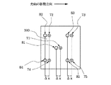
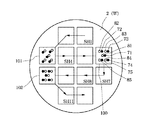
図1は本発明の一実施例に係る自動焦点合せ装置を備えた縮小投影露光装置の一部分の要部概略図である。図1において、1は縮小投影レンズであり、その光軸は図中AXで示している。縮小投影レンズ1はレチクル(不図示)の回路パターンを例えば1/5倍に縮小して投影し、その焦平面に回路パターン像を形成する。また、光軸AXは図中のz軸方向と平行な関係にある。2は表面にレジストを塗布したウエハであり、先の露光工程で互いに同じパターンが形成された多数個の被露光領域(ショット)が配列している。3はウエハを載置するウエハステージである。ウエハ2はウエハステージ3に吸着・ 固定されている。ウエハステージ3は、x軸方向に動くxステージと、y軸方向に動くyステージと、z軸方向および各x、y、z軸方向に平行な軸のまわりに回転するθ・レベリングステージで構成している。また、x、y、z軸は互いに直交するように設定してある。従って、ウエハステージ3を駆動することにより、ウエハ2の表面の位置を縮小投影レンズ1の光軸AX方向および光軸AXに直交する平面に沿った方向に調整し、さらに焦平面、すなわち回路パターン像に対する傾きも調整している。図1における符番4〜11はウエハ2の表面位置および傾きを検出するために設けた検出手段の各要素を示している。4は照明用光源、例えば発光ダイオード、半導体レーザなどの高輝度な光源である。5は照明用レンズである。光源4から射出した光は照明用レンズ5によって平行な光束となり、複数個(例えば5個)のピンホールを形成したマスク6を照明する。マスク6の各ピンホールを通過した複数個の光束は、結像レンズ7を経て折曲げミラー8に入射し、折曲げミラー8で方向を変えた後、ウエハ2の表面に入射している。ここで結像レンズ7と折曲げミラー8はウエハ2上にマスク6の複数個のピンホールの像を形成している。複数個のピンホールを通過した光束は、図2に示すようにウエハ2の被露光領域100の中央部を含む5ケ所(71〜75)を照射し、各々の箇所で反射される。すなわち、本実施例ではマスク6にピンホールを5組形成し、被露光領域100内で、後述するようにその中央部を含む5ケ所の測定点(71〜75)の位置を測定している。ウエハ2の各測定点(71〜75)で反射した光束は折曲ミラー9により方向を変えた後、検出レンズ10を介して素子を2次元的に配置した位置検出素子11上に入射する。ここで検出レンズ10は結像レンズ7、折曲げミラー8、ウエハ2、折曲げミラー9と協働してマスク6のピンホールの像を位置検出素子11上に形成している。すなわちマスク6とウエハ2と位置検出素子11は互いに光学的に共役な位置にある。
【0016】
図1では模式的に示してあるが、光学配置上困難な場合には位置検出素子11を各ピンホールに対応して複数個配置しても良い。位置検出素子11は2次元的なCCDなどから成り、複数個のピンホールを介した複数の光束の位置検出素子11の受光面への入射位置を各々独立に検知することが可能となっている。ウエハ2の縮小投影レンズ系1の光軸AX方向の位置の変化は、位置検出素子11上の複数の光束の入射位置のズレとして検出できるため、ウエハ2の被露光領域100内の5つの測定点(71〜75)における、ウエハ表面の光軸AX方向の位置が、位置検出素子11からの出力信号として面位置検出装置14を介して制御装置13へ入力している。ウエハステージ3のx軸およびy軸方向の変位はウエハステージ上に設けた基準ミラー15とレーザ干渉計17とを用いて周知の方法により測定し、ウエハステージ3の変位量を示す信号をレーザ干渉計17から信号線を介して制御装置13へ入力している。またウエハステージ3の移動はステージ駆動装置12により制御される。ステージ駆動装置12は、信号線を介して制御装置13から指令信号を受け、この信号に応答してウエハステージ3をサーボ駆動している。ステージ駆動装置12は第1駆動手段と第2駆動手段を有し、第1駆動手段によりウエハ2の光軸AXと直交する面内における位置(x,y)と回転(θ)とを調整し、第2駆動手段によりウエハ2の光軸AX方向の位置(z)と傾き(α,β)とを調整している。面位置検出装置14は位置検出素子11からの出力信号(面位置データ)を基に処理し、ウエハ2の表面の位置を検出する。そしてこの検出結果を制御装置13へ転送し所定の指令信号によりステージ駆動装置12の第2駆動手段が作動し、第2駆動手段がウエハ2の光軸AX方向の位置と傾きを調整する。
【0017】
次に本実施例におけるフォーカス検出位置について説明する。本実施例では基本的に補正駆動量算出に用いる移動中計測点と、前記位置での計測値を露光位置での計測値と等価となるように補正することを主たる目的とするオフセット算出基準用の露光位置計測点とが設定される。最初に露光位置計測点を図2に示す。測定点71は被露光領域100のほぼ中央部にあり、露光位置では光軸AXと交わる。また、残りの測定点72〜75は被露光領域100の周辺部にある。このように通常の露光位置計測点は、ウエハ内全ショットにおいて各センサが計測する部分が各々個別に各ショット同じチップの段差形状を測定しており、像面を基準平面とした場合の各センサにおける段差形状依存のオフセット値は各センサ毎に一意に決定される。従って、従来の露光位置における位置決め状態でチップの傾斜および高さ方向の位置を検出する場合、オフセットはショット毎に変更する必要はない。
【0018】
次に移動中に計測する場合の移動中計測点の一例を図3に示す。図では光軸AXと交わる位置の測定点71の代わりに移動中は測定点81を測定している様子を示す。すなわち、ウエハは図中右から左にステップ移動しており、各測定点71〜75は移動中に計測している位置がそれぞれ81〜85というようにチップ上左の位置にシフトした位置を計測していることになる。
【0019】
このようにステップ移動中に計測を行なう場合、チップとの相対位置において露光位置とは厳密には違う段差構造を持った表面を測定していることになる。これは、図4のような12ショットしか含まないショットレイアウトでさえ5種類(左、右、右上、左上、上)の異なる計測点を持つこととなり、最大で8種類の移動中計測点を持つこととなる。またこれに加えて前記移動中計測区間での本体構造体の変化はウエハ上のショット位置(x,y)とそのときの姿勢の変形(α,β)との関係から、毎回のステップ移動による姿勢変形が同じ(α,β)としても中心からのショット位置とのかけ算で求まるz方向の変位分として各ショット異なる値となる。しかしながら、この本体変形は毎回の再現性が良いことが確認されているためにショット内段差に伴うオフセット同様にショット毎のオフセットとして管理することが可能である。
【0020】
引き続き本実施例の中で用いている2種類のステップ方式、すなわちスピード重視のステップ方式(B−タイプ)と補正精度重視のステップ方式(A−タイプ)について図5および図6のフローチャートを用いて説明する。まず図5のスピード重視のステップ方式(B−タイプ)では、S401でステップ移動を開始して、目標位置到達前の移動中計測位置に到達したか否かをS402で常に現在位置を読み込みながら判定し、移動中フォーカス計測位置に到達したと判断されるとS403にてフォーカス計測を行ない、事前に求めておいた移動中計測特有のオフセット、すなわち目標位置例えば露光位置での装置状態に対する装置変形や目標位置と異なる位置での下地の段差に起因するオフセット(以下、フォーカスオフセット1という)を用いて計測値を補正し、補正後のデータで補正駆動量を算出してS404にて補正駆動を行なう。その後S405にて指定目標位置近傍に到達するまで判定を繰り返し、近傍到達が確認されるとS406にて最終的な位置決め完了確認を行なう。
【0021】
次に図6を用いて補正精度重視のステップ方式(A−タイプ)を説明する。まずS501でステップ移動を開始して、目標位置到達前の移動中計測位置に到達したか否かをS502で常に現在位置を読み込みながら判定し、移動中フォーカス計測位置に到達したと判断されると引き続きS503にて指定目標位置近傍に到達するまで判定を繰り返し、近傍到達が確認されると初めてS504にてフォーカス計測を行ない、事前に求めておいたオフセット、すなわち目標位置例えば露光位置での下地の段差に起因するオフセット(以下、フォーカスオフセット2という)を用いて計測値を補正し、補正後のデータで補正駆動量を算出してS505にて補正駆動を行なう。その後S506にて最終的な位置決め完了確認を行なう。
【0022】
以上2つのステップ方式は移動中に計測を行なって早めにステージの面位置の補正を開始するか、あるいは目標位置近傍到達を待ってステージの面位置の補正を開始するかという点が異なっている。なお、図6ではS502を入れて移動中計測点到達時の処理がないことを示したがS501の後すぐS503として目標位置近傍に到達するのを待つシーケンスとしても良い。
【0023】
次に、図7のフローチャートを用いて図1の装置の露光動作を説明する。まずS701にてジョブがセレクトされ、ジョブ内に記載されているショットのレイアウト情報を用いて前記した精度重視のステップ方式(A−タイプ:露光位置あるいはAA観察位置等に到達した位置でフォーカス補正を実施する)とスピード重視のステップ方式(B−タイプ:移動中計測位置でフォーカス補正を実施する)のどちらのステップ方式を用いるかをショット毎に判定し選択していく。具体的にはウエハのステップ方向をx軸方向にとった場合、その行の両端のショットは精度重視のA−タイプをセットしその他のショットはスピード重視のB−タイプにセットしておく。例えば図4のようなショット配列のイメージであればSH4,SH5,SH8,SH9をB−タイプに設定し、残る8ショットをA−タイプに設定する。この例のようにショット数が少ない場合にはA−タイプの比率が高くなるが、本来この実施例で説明するようなステップ移動方式の選別が必要な大径ウエハ、例えば300mmウエハでの256Mチップの露光を考えた場合、全96ショット中76ショット(約80%)はB−タイプのスピード重視のステップを選択することができる。実際の量産段階でのレイアウトの状況を考慮すると、さらにシュリンク、カットダウンが進行しているためさらに比率は向上してくるが、逆に一つ内側のチップ精度に関してもA−タイプにすべき場合がでてくる可能性がある。その場合の判定方法としてはチップ位置座標のステップ方向軸座標すなわちx軸方向へのステップ移動であればそのショットのx座標をある閾値で判定してステップ方式の判別を行なっても良い。以上のような判定方法等により各ショットのステップ方式を選択し、次にS703でロット内のウエハを搬入し、何枚目かのチェックを行ない、セットされたウエハがロットの一枚目の場合にはS704にて上記2つのステップ方式のフォーカス計測に必要なフォーカスオフセットを従来と同じ方法で測定する。以上でロット内で処理するウエハ各ショットでのステップ方式とそれに用いるフォーカスオフセットの測定が完了する。
【0024】
以下、ロット内での各ウエハ露光処理の手順を説明する。S705にて次の露光ショットへの移動の準備を行ない、当該ショットの位置、ステップ方式、フォーカスオフセットの設定等を行なう。S705でそのステップ方式のチェックを行ない、精度優先ステップの場合にはA−タイプで、速度優先ステップの場合にはB−タイプでステップ移動するようにステップ方式を切り換える。S708で露光前の位置決め位置最終確認を行ない、S709にて露光を行なう。S710で全ショットの露光完了をチェックし、終了していなければS705〜S709のフローを繰り返す。全ショットの露光が完了した場合にはS711にてウエハの搬出を行ない、ロット完了でなければS703に戻り、次のウエハロードを行なって上記露光フローを継続する。
【0025】
実施例2
露光装置上でのフォーカス検出を行なう状況としては、前記したような露光時にレチクルパターンをウエハ上に連続的にステップアンドリピートを繰り返しながら投影露光する場合のみならず、ユーザのテストコマンド実行等のオペレーションが介在し露光が中断した後に露光シーケンスに復帰する場合や、グローバルアライメント計測などウエハ上やステージ上の位置を示すマークを計測しその後再び露光シーケンスに復帰する場合にも使用されるが、このような場合には、ステップ距離が長いためにウエハの変形分の凹凸があったりオペレーションの介在がある等の理由によりz方向の位置が保証されずフォーカスの検出レンジが連続的なステップアンドリピー卜の検出範囲より広い必要がある。また前記したような連続的な露光時とは異なる計測の場合には、その計測位置がウエハの周辺になる場合が多いことも考えられる。
以上述べたように連続的な露光を行なうステップとそれ以外のステップ移動においてはその精度やスピードに関する要求スペックが異なっており、後者の場合には検出域を広げた静止位置での確実なフォーカス計測および補正を行なうA−タイプのステップを行なう必要がある。
【0026】
以下、図8を用いて第2の実施例を説明する。図8はステップ移動を実行するためのソフトウエアプログラムの機能モジュールを示している。このモジュールが起動される前段階として上記説明したステップ移動の開始トリガ、すなわち条件として以下のようなものがある。まず第1に、ユーザオペレーションが介在した場合には連続ステップの条件が崩れてしまい、次ショットへのステップはA−タイプのステップを選択することとなる。この場合、ユーザオペレーションの入力を検出し内部的なステップ方式選択フラグをオン(A−タイプ選択)と設定する。またグローバルアライメント計測などは、内部的にシーケンスが決定されているためにソフト的に前記ステップ方式選択フラグをオンと設定することが可能である。以上のように外部オペレーションや内部シーケンスの判定によりシーケンス中の各ステップに対する前記ステップ方式選択フラグがセットされる。
【0027】
このような条件のもと図8のステップ移動のための機能モジュールがコールされてS801で起動され、S802にてステップに必要な情報例えば目標位置などをセットする。次にS803で前記特殊なステップが必要な場合にセットされるステップ方式選択フラグをチェックしオン(A−タイプ選択)であればS804でフォーカス検出域の拡大を行なってS805で精度重視のA−タイプのステップ方式を実行する。フラグがオフであれば連続的なステップであるので、S805でスピード重視のB−タイプのステップ方式を起動する。いずれのステップ方式を選択した場合もS805で位置決め完了確認後、S806でステップ方式選択フラグをオフしてステップ移動を終了する。
【0028】
以上の説明においては、ステップ方式選択フラグがオンの場合、計測域の拡大を行なっていたが、計測時間がレンジに依存しない検出器すなわちPSD(位置検出ダイオード)等のアナログセンサの場合には、検出域共通のまま振動の影響を受けにくいA−タイプとオフセットが事前に測定されている必要があるB−タイプのステップとの選択を行なうようにしても良い。
【0029】
実施例3
以下、本発明の第3の実施例を説明する。本実施例のハードウエア構成は、上記実施例1と共通である。
本実施例に係るステップ方式の1つである前記自動判定用精度重視ステップ方式(C−タイプ)を図1〜4を参照しながら図10のフローチャートで詳細に説明する。まず前記露光ショットがレンズ下露光位置に来るようにステージ目標位置を制御装置13に設定後ウエハステージ3の移動を開始する(S1001)。次にレーザ干渉計17および制御装置13にて前記露光ショット位置を監視し、前記露光ショットが移動中面位置検出に適した所定位置に到達すると、前記面位置検出装置にてl度目の面位置検出(移動中面位置検出)を行なう(S1002)。
【0030】
前記移動中面位置検出は前記ステージ目標位置での該露光エリアの像面位置に対する面位置を検出するものであるが、本ステップ方式(C−タイプ)では、前記検出結果はステージ移動中の面位置検出精度を算出することを主たる目的とし、ウエハ2の高さおよび傾きの調整には使用しない。以上でステージ移動中の動作を終了し、ウエハステージ3の位置決め終了確認(S1003)後、前記面位置検出装置にて2度目の面位置検出(静止面位置検出)を行なう(S004)。前記静止面位置検出後に検出結果を使ってウエハ2の高さおよび傾き調整を行なう(S1005)。そして、前記移動中面位置検出結果を前記フォーカスオフセット1を用いて補正したデータと前記静止面位置検出結果を前記フォーカスオフセット2を用いて補正したデータの差分から移動中面位置検出結果を使ってウエハ2の高さおよび傾き調整を行なった場合の露光像面に対する誤差(移動中面位置検出誤差)を算出し制御装置13に露光エリア毎に分類して格納する(S1006)。
【0031】
次に本実施例のステップ方式の1つである自動判定用スピード重視ステップ方式(D−タイプ)を図11のフローチャートで詳細に説明する。まず前記ステップ方式(C−タイプ)と同様にステージ目標位置を制御装置13に設定後ウエハステージ3の移動を開始する。同じくC−タイプと同様に所定位置にてl度目の面位置検出(移動中面位置検出)を行ない(S1102)、検出結果を前記補正オフセットを用いて補正したデータを用いてウエハ2の高さおよび傾き調整を行なう(S1103)。前記調整後、ウエハステージ3の位置決め終了確認(Sll04)を待ち、前記面位置検出装置にて2度目の面位置検出(静止面位置検出)を行なう(S1105)。前記静止面位置検出は前記移動中面位置検出結果による前記高さおよび傾き調整の誤差を測定することを主たる目的とするものでウエハ2の高さおよび傾きの調整には使用しない。最後に本実施例では前記静止面位置検出結果から移動中面位置検出誤差を算出し、制御装置13に各露光エリア毎に分類して格納する(Sll06)。
【0032】
以上のようなステップ方式を用いる本実施例を図9のフローチャートを用いて詳細に説明する。
まずS901にて不図示のウエハ供給手段によりパターン付きのウエハ2をウエハステージ3に供給し、S902にて不図示のアライメント機構によりウエハ2の光軸AXおよびウエハステージ3の基準配列に対するxy方向の位置ずれを計測し、ウエハ上に転写されたショット配列の格子に合わせてステップするための格子を算出し、制御装置13に格納する。これにより、露光位置における各ショットでの各フォーカスセンサ毎の段差形状依存によるオフセットが一意に決定できるようになる。続いてウエハが1枚目であれば(S903)、露光位置のフォーカス検出値から露光位置の像面基準の面位置を算出するための計測オフセットと移動中のフォーカス検出値から露光位置の像面基準の面位置を算出するための計測オフセット等を算出する(S904)。これにより、露光位置やステージ移動中所定位置における、露光位置での像面位置基準の面位置検出が正確に行なえる。
【0033】
次にS905で前記制御装置13は格納された前記移動中面位置検出誤差の履歴から前記移動中面位置検出精度を計算し閾値等で判定することでC−タイプまたはD−タイプのステップ方式の選択を自動で行なう。
【0034】
前記選択は2枚目以降の新たなウエハが搬入されるたびにそれまでに蓄積された前記移動中面位置検出誤差の履歴から全ショットにおいて自動で行なうもので、ウエハ処理枚数が増せば履歴データも増えるので信頼度も自動的で高まる特徴を持つ。これにより従来の経験に基づく選択に比べ高精度で即時性の高い選択が可能である。
以上のステップ方式の自動選択結果を踏まえ次の露光ショットがレンズ下露光位置に来るようにステージ目標位置を制御装置13に設定後ウエハステージ3の移動を開始(S906)する。該露光ショットの前記ステップ方式の自動選択結果に基づき前記C−タイプのステップ方式(S909)またはD−タイプのステップ方式(S908)を実行する。以上のようなステップ方式で全6軸の位置決め完了確認後、S910で露光を行なう。S911では全ショットの露光が終了したか否かのループ管理を行ない、該ウエハの全ショットの露光が終了していなければ、次の露光ショットにウエハステージ移動を行ない(S906)、終了していればウエハステージ3上のウエハの搬出を行なう(S912)。同様にS913では全ウエハの露光が終了したか否かのループ管理を行ない、終了していなければ次ウエハを搬入し(S901)、終了していれば処理を終了する。
【0035】
以上の実施例の中で、ショットにより精度重視のステップ方式に途中で切り換わるショット位置などは装置的に不安定な状態にある可能性があり、また全体的なチップの生産効率が変化している場合などこのステップ方式の自動選択の影響によりスピード重視ステップの比率が低下していることが考えられる。このような場合には装置のメンテナンス例えばチャックのクリーニングやステージのチューニングなどを行なえば元のチップ生産効率に戻すことが可能となる。このような状況に対処するために本実施例では以下のような方法を用いている。
すなわち、図1において、制御装置13に接続された不図示のホストターミナルに対してロットの処理に関して各ウエハ毎の処理情報に関するデータべースを構築し、その中で前記ステップ方式が変更されたショットに関してYes/Noの情報を保持していく方法をとっている。オペレータはロット処理後その処理時間や補正精度をチェックするとともにこのデータベースを閲覧することにより装置メンテナンスの必要性を判断することができる。また別の通知方法としては、ロットの処理中に前記ステップ方式の切り換え頻度およびスピード重視ステップ方式のウエハ内の比率等を算出し、ある閾値を元に判断を行ない、通知すべきと判断した場合には、前記ホストターミナル画面上或いは別の表示手段を用いてオペレータに即時通知を行なう。前記閾値に関しては処理されるロットの必要精度によりオペレータが随時変更することが可能である。
【0036】
実施例4
次に本発明の第4の実施例を説明する。本実施例の露光装置では移動中面位置検出時の精度のばらつきの主原因であるステージの振動を計測するための手段を備える。前記振動計測手段として例えば静電容量センサ等を使用すれば、リアルタイムで傾き計測が可能である。これにより本実施例では、各露光ショットのステップ時に前記移動中面位置検出中のステージ振動を前記振動計測手段にて計測する。次ウエハの各露光ショットのステップ時には前記計測した振動計測値に基づきステップ方式を選択する。本実施例を用いれば移動中面位置検出時の精度のばらつきの主原因であるステージ振動そのものをステップ方式の判断基準に使うので、例えばウエハ1枚の振動計測値からでも移動中面位置検出時の精度が推測可能であり、早い時期にステップ方式の判定が可能である。
【0037】
【デバイス生産方法の実施例】
次に上記説明した露光装置または露光方法を利用したデバイスの生産方法の実施例を説明する。
図12は微小デバイス(ICやLSI等の半導体チップ、液晶パネル、CCD、薄膜磁気ヘッド、マイクロマシン等)の製造のフローを示す。ステップ1(回路設計)ではデバイスのパターン設計を行なう。ステップ2(マスク製作)では設計したパターンを形成したマスクを製作する。一方、ステップ3(ウエハ製造)ではシリコンやガラス等の材料を用いてウエハを製造する。ステップ4(ウエハプロセス)は前工程と呼ばれ、上記用意したマスクとウエハを用いて、リソグラフィ技術によってウエハ上に実際の回路を形成する。次のステップ5(組み立て)は後工程と呼ばれ、ステップ4によって作製されたウエハを用いて半導体チップ化する工程であり、アッセンブリ工程(ダイシング、ボンディング)、パッケージング工程(チップ封入)等の工程を含む。ステップ6(検査)ではステップ5で作製された半導体デバイスの動作確認テスト、耐久性テスト等の検査を行なう。こうした工程を経て半導体デバイスが完成し、これが出荷(ステップ7)される。
【0038】
図13は上記ウエハプロセスの詳細なフローを示す。ステップ11(酸化)ではウエハの表面を酸化させる。ステップ12(CVD)ではウエハ表面に絶縁膜を形成する。ステップ13(電極形成)ではウエハ上に電極を蒸着によって形成する。ステップ14(イオン打込み)ではウエハにイオンを打ち込む。ステップ15(レジスト処理)ではウエハに感光剤を塗布する。ステップ16(露光)では上記説明した面位置検出方法を採用した露光装置によってマスクの回路パターンをウエハに焼付露光する。ステップ17(現像)では露光したウエハを現像する。ステップ18(エッチング)では現像したレジスト像以外の部分を削り取る。ステップ19(レジスト剥離)ではエッチングが済んで不要となったレジストを取り除く。これらのステップを繰り返し行なうことによって、ウエハ上に多重に回路パターンが形成される。
【0039】
本実施例の生産方法を用いれば、従来は製造が難しかった高集積度のデバイスを低コストに製造することができる。
【0040】
【発明の効果】
以上説明したように本発明によれば、高精度で高速な面位置検出技術を提供することができる。
【図面の簡単な説明】
【図1】本発明の一実施例に関わるステップアンドリピート方式の縮小投影露光装置の部分的概略図である。
【図2】本発明の一実施例における被露光領域中に設定した露光位置測定点の配置を示す説明図である。
【図3】本発明の一実施例における被露光領域中に設定した移動中計測点の配置を示す説明図である。
【図4】ウエハ上にレイアウトされた露光位置と各測定位置の対応およびショット間のステップ移動の様子を説明する説明図である。
【図5】本発明の第1の実施例に関わる、スピード優先のステップ移動の方法を説明するフローチャート図である。
【図6】本発明の第1の実施例に関わる、精度優先のステップ移動の方法を説明するフローチャート図である。
【図7】本発明の第1の実施例に関わる、レイアウト情報に基づきショット毎にステップ方式を切り換える一例を示すフローチャート図である。
【図8】本発明の第1の実施例に関わる、ステップ方式の選択動作の一例を示すフローチャート図である。
【図9】本発明の第3の実施例に関わる、図1の装置による過去のステップ履歴情報に基づきショット毎にステップ方式を自動で切り換える一例を示すフローチャート図である。
【図10】本発明の第3の実施例に関わる、図1の装置によるステップ方式の選択動作の一例(C−タイプ)を示すフローチャート図である。
【図11】本発明の第3の実施例に関わる、図1の装置によるステップ方式の選択動作の一例(D−タイプ)を示すフローチャート図である。
【図12】微小デバイスの製造の流れを示す図である。
【図13】図12におけるウエハプロセスの詳細な流れを示すフローチャート図である。
【符号の説明】
1:縮小投影レンズ、2:ウエハ、3:ウエハステージ、4:高輝度光源、5:照明用レンズ、6:ピンホールを持つマスク、7,10:結像レンズ、8,9:折り曲げミラー、11:2次元検出素子、12:ステージ駆動装置、13:制御装置、14:面位置検出装置、71〜75:露光位置測定点、81〜85:移動中計測点、100〜102:被露光領域。[0001]
TECHNICAL FIELD OF THE INVENTION
The present invention relates to an exposure apparatusThrowShadowOptical system optical axisThe present invention relates to a surface position detection technique for detecting a surface position of an exposed region of a substrate in a direction.
[0002]
[Prior art]
There is an improvement in productivity as a performance strongly demanded in recent semiconductor manufacturing apparatuses, in particular, a successively moving semiconductor exposure apparatus called a stepper. That is, it is necessary for the chip maker to reduce the unit cost of the chip so that the memory cost commensurate with the chip replacement can be presented with the increase in the integration rate according to the memory trend.
Exposure equipment manufacturers must provide equipment that can contribute not only to high performance but also to improved productivity. It is required to increase the number of processed sheets.
[0003]
Under such circumstances, as a method of shortening the step time of a semiconductor exposure apparatus currently used in a production site, the present applicant has disclosed in Japanese Patent Publication No. 4-50731 and Japanese Patent Laid-Open Publication No. 4-116414 the position and inclination of the substrate surface during the step. And a method of detecting and correcting it. By using this method, the start timing of the surface position correction is earlier than in the conventional method of confirming that the exposure position has been positioned and detecting the position and inclination, so that the entire step time can be reduced. It becomes possible.
In addition, a focus offset for correcting the measurement value at the measurement position during the movement to be equivalent to the measurement value at the exposure position is calculated in advance, and the surface position measurement value during the movement is positively used for the step time. It has been proposed to introduce a method of shortening the measurement time or a method of shortening the measurement time by performing measurement with limiting the focus detection range in consideration of the continuous steps, and further reduce the step time.
[0004]
[Problems to be solved by the invention]
Up to the present, in the process design of semiconductor manufacturing, the exposure wavelength of an exposure apparatus has been selected in accordance with a wiring rule. That is, a manufacturing line has been constructed by using the exposure wavelength used as the limit of the resolution line width, such as an i-line stepper for the 0.35 μm rule and a KrF stepper for the 0.25 μm rule. (Budget) also continued to share about 1.0 μm between the apparatus and the process. However, a policy has been set forth that a KrF exposure apparatus will be continuously used as an exposure technique in the next-generation 0.18 μm rule. There is also a movement to extend the life of KrF exposure until mass production of 1 giga DRAMs with the 1 μm rule. To this end, in addition to the development of technology for miniaturization such as a phase shift mask and super-resolution, the improvement of the flatness in a chip by employing CMP (chemical mechanical polish) has greatly contributed. It has been reported that the chip step in the case of forming a trench structure by using CMP can be settled to about 50 nm, and it is possible to design a conventional high NA lens with a reduced focal depth at a stretch and to provide a resolution below the wavelength. It has become possible.
[0005]
However, on the other hand, it is necessary to further improve the correction accuracy of the focus leveling in order to reduce the depth of focus accompanying the increase in the NA. In other words, the method of guaranteeing the chip level difference on the process side has begun to be diversified by various companies such as CMP, PSM (phase shift mask), and RA (recessed array). Production is about to begin with a different depth margin. Therefore, in a specific process of the user, particularly in a process in which complete flattening is difficult due to the stack method, there may be a case where a higher correction accuracy than before is required. In such a method, the offset reproducibility is slightly different depending on the position on the wafer, so that the correction accuracy may not satisfy the standard depending on the position of the shot on the wafer. The main cause is that the external shape of the wafer itself is scaled up for 300 mm wafers, etc., and as the structural deformation in the tilt direction of the stage expands in the radial direction of the wafer, the vibration in the z direction increases. The difference lies in the reproducibility of the offset at the time. This instability is within an allowable range if the conventional accuracy is used, but it becomes an insignificant amount when the above-described residual chip step is covered on the device side. Further, in the conventional method of performing a focusing operation by limiting the focus detection area in order to reduce the step time, in a sequence other than the exposure, for example, global alignment measurement or a step command after a user operation is executed, In some cases, the sequence may stop due to the case where the surface to be detected exceeds the focus detection range.
[0006]
The purpose of the present invention is,In view of such problems of the prior art,HighAccurate and fastFacePosition detectionTechnologyIs to provide.
[0007]
[Means for Solving the Problems]
To this end, the present invention providesVia projection opticsA method for detecting a surface position used in an exposure apparatus that projects a pattern on a substrate, comprising:Optical axis of optical systemOrthogonal to the direction ofOneDuring the movement of the substrate to position the exposed area on the substrate in theoptical axisA first detection mode for detecting a position of the exposed region in a direction, and after the positioning,optical axisSelecting one of a second detection mode for detecting the position of the exposed area in the direction, based on a detection result in the detection mode selected in the selecting step, for each of the exposed areas. Detecting a surface position to be exposed as a surface position of the exposed region. Such a surface position detection method is suitably applied particularly to a sequentially moving exposure apparatus.
[0008]
Also, the present inventionVia projection opticsAn exposure apparatus for projecting a pattern on a substrate, wherein the projection apparatusOptical axis of optical systemFirst detecting means for detecting the position of the region to be exposed on the substrate in the direction ofoptical axisOrthogonal to the directionOneA first detection mode in which detection is performed by the first detection means while the substrate is moving in order to position a region to be exposed on the substrate, and a detection by the first detection means is performed after the positioning. Selecting means for selecting one of the second detection modes for each of the areas to be exposed, and setting the surface position obtained based on the detection result in the detection mode selected by the selecting means to the surface position of the area to be exposed And a second detection unit that detects the second detection.
[0009]
BEST MODE FOR CARRYING OUT THE INVENTION
In the exposure apparatus according to the first preferred embodiment of the present invention, the projection optical system moves along a direction substantially orthogonal to the optical axis of the projection optical system while the wafer is mounted on the exposure optical system, and A stage that sends the predetermined surface of the wafer to the image plane, a detector that detects at least one of a position and an inclination of the predetermined position of the wafer in the optical axis direction, and the predetermined surface of the projection optical system based on a value detected by the detector. An exposure apparatus having focusing means for focusing on a focal plane, a step method (B) of focusing the predetermined detection surface on a predetermined setting surface based on surface position information measured during movement, and the predetermined detection surface (A) that focuses on a predetermined setting surface based on surface position information in a state where is substantially positioned at a predetermined position.
[0010]
In this way, the speed-oriented step method (B) of focusing the predetermined detection surface on the predetermined setting surface based on the surface position information measured during the movement, and in a state where the predetermined detection surface is substantially positioned at the predetermined position. The above two steps are used in a situation where the above problem occurs due to having two steps of the step method (A) which focuses on the predetermined setting surface based on the surface position information and the accuracy. Problem can be solved.
[0011]
In addition, regarding the selection of the two step methods, a step method is set for each shot based on layout information in advance, and each shot is focused on a predetermined setting surface according to the set method, thereby achieving high-speed and high-precision chip exposure. Can be automatically designed.
[0012]
Further, it is possible to avoid a situation where the sequence is stopped by selecting one of the two step methods based on the state of the stage position immediately before the start of the step, moving the step, and focusing on a predetermined setting surface. Will be possible.
[0013]
The focus detection means in the two-step method can change the detection range and the detection time by switching the focus detection range according to the step method.West,In consideration of the entire processing time, it is possible to create a job of a chip treatment that achieves both accuracy and productivity.
[0014]
In the exposure apparatus according to the second preferred embodiment of the present invention, the wafer is moved along a direction substantially perpendicular to the optical axis of the projection optical system while the wafer is mounted, and a predetermined detection area of the wafer is moved by the projection optical system. A stage for feeding the wafer to an image plane; a detector for detecting at least one of a position and an inclination of a predetermined position of the wafer with respect to the optical axis direction; and a focus of the projection optical system based on a value detected by the detector. An exposure apparatus having a focusing unit for focusing on a plane, wherein the step of focusing the predetermined detection target surface on a predetermined setting surface based on surface position information measured during movement and a step of testing the correction accuracy for automatic determination. A step method (D) emphasizing speed and a step method (C) emphasizing accuracy for focusing on a predetermined setting surface based on surface position information when the predetermined detection target surface is substantially positioned at a predetermined position. Chi, to solve the above problem by automatically selecting an optimum step mode from each shot measurement history up to that in one aspect the problem occurs. For example, when it is determined from the history of the moving surface position information during the step moving method (C) that the correction accuracy can be sufficiently obtained by the step method (D), the step method is changed to the step method (D). When the step moving method (D) determines that sufficient correction accuracy cannot be obtained from the history of the post-focus position information of the predetermined surface during the switching and the step moving method (D), the step method is used. Switch to step method (C). Therefore, for example, if the step method of each exposure shot is set to the step method (C) for the first wafer of the lot and the switching between the two step methods is constantly performed, an exposure method having a high-precision and high-speed surface position detection correction method can be achieved. Location can be provided.
[0015]
【Example】
Hereinafter, embodiments of the present invention will be described with reference to the drawings.
Example 1
FIG. 1 is a schematic view showing a main part of a part of a reduction projection exposure apparatus provided with an automatic focusing apparatus according to one embodiment of the present invention. In FIG. 1, reference numeral 1 denotes a reduction projection lens whose optical axis is indicated by AX in the figure. The reduction projection lens 1 projects a circuit pattern of a reticle (not shown) at a reduced size of, for example, 1/5, and forms a circuit pattern image on the focal plane. Further, the optical axis AX is in a relationship parallel to the z-axis direction in the figure.
[0016]
Although schematically shown in FIG. 1, if it is difficult to arrange optically, a plurality of
[0017]
Next, the focus detection position in this embodiment will be described. In this embodiment, a moving measurement point basically used for calculating a correction drive amount and an offset calculation reference mainly for correcting the measurement value at the position so as to be equivalent to the measurement value at the exposure position. Of exposure position measurement points are set. First, the exposure position measurement points are shown in FIG. The
[0018]
Next, an example of a measurement point during movement when measuring during movement is shown in FIG. The figure shows a state in which the
[0019]
When the measurement is performed during the step movement as described above, a surface having a step structure strictly different from the exposure position is measured at a position relative to the chip. This means that even a shot layout including only 12 shots as shown in FIG. 4 has five different measurement points (left, right, upper right, upper left, and upper), and has a maximum of eight types of moving measurement points. It will be. In addition to this, the change of the main body structure in the measurement section during the movement is caused by each step movement from the relationship between the shot position (x, y) on the wafer and the deformation (α, β) of the posture at that time. Even if the posture deformation is the same (α, β), each shot has a different value as a displacement in the z direction obtained by multiplication with the shot position from the center. However, since it has been confirmed that the reproducibility of the main body deformation is good every time, it is possible to manage the main body deformation as an offset for each shot in the same manner as an offset due to a step in a shot.
[0020]
Referring to the flowcharts of FIG. 5 and FIG. 6, two types of step methods continuously used in the present embodiment, that is, a step method that emphasizes speed (B-type) and a step method that emphasizes correction accuracy (A-type) will be described. explain. First, in the speed-oriented step method (B-type) shown in FIG. 5, step movement is started in S401, and it is determined in S402 whether or not the movement measurement position before reaching the target position is reached while always reading the current position. Then, when it is determined that the focus measurement position during the movement has been reached, focus measurement is performed in S403, and an offset peculiar to the measurement during the movement obtained in advance, that is, a target position, for example, an apparatus deformation with respect to the state of the apparatus at the exposure position, The measured value is corrected using an offset (hereinafter, referred to as focus offset 1) caused by a step on the base at a position different from the target position, a corrected drive amount is calculated based on the corrected data, and the correction drive is performed in S404. . Thereafter, in S405, the determination is repeated until the vehicle reaches the vicinity of the designated target position, and when it is confirmed that the vehicle has reached the vicinity of the designated target position, the final positioning completion is confirmed in S406.
[0021]
Next, a step method (A-type) that emphasizes correction accuracy will be described with reference to FIG. First, a step movement is started in S501, and it is determined whether or not the moving position before reaching the target position is reached while the current position is always read in S502. Subsequently, the determination is repeated until reaching the vicinity of the designated target position in S503, and when arrival in the vicinity is confirmed, focus measurement is performed in S504 for the first time, and the offset obtained in advance, that is, the offset of the base at the target position, for example, the exposure position, is determined. The measured value is corrected using an offset due to the step (hereinafter, referred to as focus offset 2), a corrected drive amount is calculated based on the corrected data, and the correction drive is performed in S505. After that, the final positioning completion confirmation is performed in S506.
[0022]
The above two step methods differ in that measurement is performed during movement and correction of the stage surface position is started earlier, or correction of the stage surface position is started after reaching the target position. . In FIG. 6, S502 is inserted to indicate that there is no processing at the time of reaching the measurement point during the movement. However, immediately after S501, a sequence of waiting for reaching to the vicinity of the target position may be performed as S503.
[0023]
Next, the exposure operation of the apparatus of FIG. 1 will be described with reference to the flowchart of FIG. First, in step S701, a job is selected, and the focus correction is performed using the layout information of the shots described in the job and focusing on the accuracy-based step method (A-type: exposure position or AA observation position). It is determined and selected for each shot as to which of the step method of performing the focus correction and the step method of emphasizing the speed (B-type: performing the focus correction at the moving measurement position) is used. More specifically, when the step direction of the wafer is taken in the x-axis direction, the shots at both ends of the row are set to the A-type, which emphasizes accuracy, and the other shots are set to the B-type, which emphasizes speed. For example, in the case of the shot arrangement image as shown in FIG. 4, SH4, SH5, SH8, and SH9 are set to B-type, and the remaining eight shots are set to A-type. When the number of shots is small as in this example, the ratio of the A-type becomes high, but a large-diameter wafer that originally needs to be sorted by the step moving method as described in this embodiment, for example, a 256-M chip with a 300 mm wafer Considering the exposure of (1), a B-type speed-oriented step can be selected for 76 shots (about 80%) of all 96 shots. Considering the layout situation at the actual mass production stage, the ratio is further improved due to further shrinkage and cut-down, but on the other hand the chip accuracy inside one should also be A-type May come out. As a determination method in this case, if the step movement is in the step direction axis coordinate of the chip position coordinate, that is, in the x-axis direction, the x coordinate of the shot may be determined using a certain threshold value to determine the step method. When the step method of each shot is selected by the above-described determination method or the like, the wafers in the lot are loaded in step S703, and some wafers are checked, and the set wafer is the first wafer in the lot. In step S704, the focus offset required for the focus measurement in the two-step method is measured in the same manner as in the related art. Thus, the step method for each shot of the wafer processed in the lot and the measurement of the focus offset used for the step method are completed.
[0024]
Hereinafter, the procedure of each wafer exposure process in a lot will be described. In step S705, a preparation for moving to the next exposure shot is made, and the position, step method, focus offset, and the like of the shot are set. In step S705, the step method is checked, and the step method is switched so that the step movement is performed in the A-type in the case of the accuracy priority step and in the B-type in the case of the speed priority step. In S708, the final confirmation of the positioning position before exposure is performed, and in S709, exposure is performed. In step S710, it is checked whether exposure of all shots has been completed. If the exposure has not been completed, the flow of steps S705 to S709 is repeated. If the exposure for all shots has been completed, the wafer is unloaded in S711, and if not, the process returns to S703 to load the next wafer and continue the above exposure flow.
[0025]
Example 2
The focus detection on the exposure apparatus is performed not only when the reticle pattern is projected and exposed on the wafer while continuously repeating the step-and-repeat at the time of exposure as described above, but also when a user executes a test command or the like. It is also used to return to the exposure sequence after exposure is interrupted due to the presence of, or to return to the exposure sequence again after measuring marks indicating positions on the wafer or stage, such as global alignment measurement. In such a case, the position in the z direction is not guaranteed due to the presence of irregularities corresponding to the deformation of the wafer or the presence of operation due to a long step distance, and the focus detection range is a continuous step-and-repeat. Must be wider than the detection range. In the case of measurement different from that at the time of continuous exposure as described above, the measurement position is often considered to be around the wafer.
As described above, the required specifications regarding accuracy and speed are different between the step of performing continuous exposure and the other step movements, and in the latter case, reliable focus measurement at a stationary position with a wider detection area And an A-type step of performing the correction.
[0026]
Hereinafter, the second embodiment will be described with reference to FIG. FIG. 8 shows functional modules of a software program for performing the step movement. As a stage before this module is activated, the start trigger of the step movement described above, that is, the following conditions are available. First, if a user operation is involved, the condition of a continuous step is broken, and an A-type step is selected for the step to the next shot. In this case, the input of the user operation is detected, and the internal step method selection flag is set to ON (A-type selection). In the global alignment measurement and the like, since the sequence is determined internally, the step method selection flag can be set to ON by software. As described above, the step method selection flag for each step in the sequence is set by the determination of the external operation or the internal sequence.
[0027]
Under these conditions, the function module for the step movement of FIG. 8 is called and started in S801, and in S802, information necessary for the step, for example, a target position is set. Next, in step S803, the step method selection flag that is set when the special step is required is checked. If the flag is on (A-type selection), the focus detection area is expanded in step S804. Performs type stepping. If the flag is off, it is a continuous step, so in step S805, the B-type step method emphasizing speed is activated. Regardless of which step method is selected, after the completion of positioning is confirmed in S805, the step method selection flag is turned off in S806, and the step movement ends.
[0028]
In the above description, when the step method selection flag is on, the measurement range is expanded. However, in the case of a detector whose measurement time does not depend on the range, that is, an analog sensor such as a PSD (position detection diode), The selection may be made between the A-type, which is less affected by vibration, and the B-type, whose offset needs to be measured in advance, while keeping the detection area common.
[0029]
Example 3
Hereinafter, a third embodiment of the present invention will be described. The hardware configuration of this embodiment is the same as that of the first embodiment.
The accuracy-oriented step method (C-type) for automatic determination, which is one of the step methods according to the present embodiment, will be described in detail with reference to the flowchart of FIG. First, after the stage target position is set in the
[0030]
The moving surface position detection is to detect the surface position of the exposure area at the stage target position with respect to the image plane position. In this step method (C-type), the detection result is the surface moving stage. Its main purpose is to calculate the position detection accuracy, and is not used for adjusting the height and tilt of the
[0031]
Next, the speed determination step method (D-type) for automatic determination, which is one of the step methods of the present embodiment, will be described in detail with reference to the flowchart of FIG. First, similarly to the step method (C-type), after the stage target position is set in the
[0032]
This embodiment using the above-described step method will be described in detail with reference to the flowchart of FIG.
First, in step S901, a
[0033]
Next, in step S905, the
[0034]
The selection is automatically performed for all shots from the history of the moving surface position detection error accumulated so far each time a second or subsequent new wafer is loaded. As a result, the reliability is automatically increased. As a result, selection with high accuracy and high immediacy can be performed as compared with selection based on conventional experience.
Based on the result of the automatic selection of the step method described above, the stage target position is set in the
[0035]
In the above embodiment, the shot position where the shot is switched to the step method that emphasizes accuracy depending on the shot may be in a device unstable state, and the overall chip production efficiency may change. For example, it is conceivable that the ratio of the speed-oriented steps is reduced due to the influence of the automatic selection of the step method. In such a case, it is possible to return to the original chip production efficiency by performing maintenance of the apparatus, for example, cleaning the chuck and tuning the stage. In this embodiment, the following method is used to cope with such a situation.
That is, in FIG. 1, a database relating to processing information for each wafer is constructed for the processing of a lot with respect to a host terminal (not shown) connected to the
[0036]
Example 4
Next, a fourth embodiment of the present invention will be described. The exposure apparatus of the present embodiment includes means for measuring the vibration of the stage, which is the main cause of the variation in accuracy when detecting the position of the moving surface. If, for example, a capacitance sensor or the like is used as the vibration measuring means, the inclination can be measured in real time. Thus, in this embodiment, the stage vibration during the movement mid-surface position detection is measured by the vibration measuring means at the time of each exposure shot step. At the time of the step of each exposure shot of the next wafer, the step method is selected based on the measured vibration value. According to this embodiment, the stage vibration itself, which is the main cause of the variation in accuracy when detecting the position of the moving surface, is used as a criterion of the step method. Can be estimated, and the step method can be determined at an early stage.
[0037]
[Example of device production method]
Next, an embodiment of a device production method using the above-described exposure apparatus or exposure method will be described.
FIG. 12 shows a flow of manufacturing micro devices (semiconductor chips such as ICs and LSIs, liquid crystal panels, CCDs, thin-film magnetic heads, micromachines, etc.). In step 1 (circuit design), a device pattern is designed. Step 2 (mask fabrication) forms a mask on which the designed pattern is formed. On the other hand, in step 3 (wafer manufacturing), a wafer is manufactured using a material such as silicon or glass. Step 4 (wafer process) is referred to as a pre-process in which an actual circuit is formed on the wafer by lithography using the prepared mask and wafer. The next step 5 (assembly) is called a post-process, and is a process of forming a semiconductor chip using the wafer produced in step 4, and includes processes such as an assembly process (dicing and bonding) and a packaging process (chip encapsulation). including. In step 6 (inspection), inspections such as an operation confirmation test and a durability test of the semiconductor device manufactured in step 5 are performed. Through these steps, a semiconductor device is completed and shipped (step 7).
[0038]
FIG. 13 shows a detailed flow of the wafer process. Step 11 (oxidation) oxidizes the wafer's surface. Step 12 (CVD) forms an insulating film on the wafer surface. Step 13 (electrode formation) forms electrodes on the wafer by vapor deposition. Step 14 (ion implantation) implants ions into the wafer. In step 15 (resist processing), a photosensitive agent is applied to the wafer. In step 16 (exposure), a circuit pattern on the mask is printed onto the wafer by exposure using an exposure apparatus that employs the above-described surface position detection method. Step 17 (development) develops the exposed wafer. In step 18 (etching), portions other than the developed resist image are removed. Step 19 (resist stripping) removes unnecessary resist after etching. By repeating these steps, multiple circuit patterns are formed on the wafer.
[0039]
By using the production method of the present embodiment, a highly integrated device, which was conventionally difficult to produce, can be produced at low cost.
[0040]
【The invention's effect】
According to the present invention as described above,High accuracy and high speed surface position detection technology can be provided..
[Brief description of the drawings]
FIG. 1 is a partial schematic view of a step-and-repeat type reduction projection exposure apparatus according to an embodiment of the present invention.
FIG. 2 is an explanatory diagram showing an arrangement of exposure position measurement points set in a region to be exposed according to an embodiment of the present invention.
FIG. 3 is an explanatory diagram showing an arrangement of moving measurement points set in a region to be exposed according to an embodiment of the present invention.
FIG. 4 is an explanatory diagram for explaining correspondence between an exposure position laid out on a wafer and each measurement position, and a state of step movement between shots.
FIG. 5 is a flowchart illustrating a speed-priority step moving method according to the first embodiment of the present invention.
FIG. 6 is a flowchart illustrating a method of precision-based step movement according to the first embodiment of the present invention.
FIG. 7 is a flowchart illustrating an example of switching a step method for each shot based on layout information according to the first embodiment of the present invention.
FIG. 8 is a flowchart illustrating an example of a step-type selection operation according to the first embodiment of the present invention.
FIG. 9 is a flowchart illustrating an example of automatically switching the step method for each shot based on past step history information by the apparatus of FIG. 1 according to the third embodiment of the present invention.
FIG. 10 is a flowchart showing an example (C-type) of a step-type selecting operation by the apparatus of FIG. 1 according to the third embodiment of the present invention.
FIG. 11 is a flowchart showing an example (D-type) of a step-type selection operation by the apparatus of FIG. 1 according to the third embodiment of the present invention.
FIG. 12 is a diagram showing a flow of manufacturing a micro device.
FIG. 13 is a flowchart showing a detailed flow of a wafer process in FIG. 12;
[Explanation of symbols]
1: reduction projection lens, 2: wafer, 3: wafer stage, 4: high brightness light source, 5: illumination lens, 6: mask having pinhole, 7, 10: imaging lens, 8, 9: bending mirror, 11: two-dimensional detection element, 12: stage driving device, 13: control device, 14: surface position detection device, 71 to 75: exposure position measurement point, 81 to 85: moving measurement point, 100 to 102: exposure area .
Claims (18)
前記投影光学系の光軸の方向に直交する方向に前記基板上の被露光領域を位置決めするための前記基板の移動中に、前記光軸方向における前記被露光領域の位置を検出する第1の検出モードと、前記位置決め後に、前記光軸方向における前記被露光領域の位置を検出する第2の検出モードとのうち一方を、前記被露光領域毎に選択する選択工程と、
前記選択工程において選択された検出モードにおける検出結果に基づいて得られる面位置を前記被露光領域の面位置として検出する検出工程と
を含むことを特徴とする面位置検出方法。 A surface position detection method used in an exposure apparatus that projects a pattern onto a substrate via a projection optical system ,
During movement of the substrate for positioning the object exposure region of the substrate in the direction perpendicular to the direction of the optical axis of the projection optical system, the first to detect the position of the area to be exposed in the optical axis direction A detection mode and, after the positioning, one of a second detection mode for detecting the position of the exposed region in the optical axis direction, a selecting step of selecting for each exposed region,
Detecting a surface position obtained based on a detection result in the detection mode selected in the selection step as a surface position of the exposed area.
前記投影光学系の光軸の方向における前記基板の被露光領域の位置を検出する第1検出手段と、
前記光軸方向に直交する方向に前記基板上の被露光領域を位置決めするための前記基板の移動中に、前記第1検出手段による検出を行う第1の検出モードと、前記位置決め後に、前記第1検出手段による検出を行う第2の検出モードとのうち一方を、前記被露光領域毎に選択する選択手段と、
前記選択手段により選択された検出モードにおける検出結果に基づいて得られる面位置を前記被露光領域の面位置として検出する第2検出手段と
を有することを特徴とする露光装置。An exposure apparatus that projects a pattern onto a substrate via a projection optical system ,
First detection means for detecting a position of an exposed region of the substrate in a direction of an optical axis of the projection optical system ;
During movement of the substrate for positioning the object exposure region of the substrate in the direction perpendicular to the optical axis direction, the first detection mode in which detection by said first detection means, after the positioning, the Selecting means for selecting one of a second detection mode for performing detection by the first detecting means for each of the exposed areas;
An exposure apparatus comprising: a second detection unit configured to detect a surface position obtained based on a detection result in the detection mode selected by the selection unit as a surface position of the exposed area.
Priority Applications (2)
| Application Number | Priority Date | Filing Date | Title |
|---|---|---|---|
| JP35405297A JP3587343B2 (en) | 1997-12-09 | 1997-12-09 | Surface position detection method, exposure apparatus and device manufacturing method |
| US09/205,173 US6163369A (en) | 1997-12-09 | 1998-12-04 | Plane position detecting method and exposing method and exposure apparatus using same |
Applications Claiming Priority (1)
| Application Number | Priority Date | Filing Date | Title |
|---|---|---|---|
| JP35405297A JP3587343B2 (en) | 1997-12-09 | 1997-12-09 | Surface position detection method, exposure apparatus and device manufacturing method |
Publications (2)
| Publication Number | Publication Date |
|---|---|
| JPH11176735A JPH11176735A (en) | 1999-07-02 |
| JP3587343B2 true JP3587343B2 (en) | 2004-11-10 |
Family
ID=18434979
Family Applications (1)
| Application Number | Title | Priority Date | Filing Date |
|---|---|---|---|
| JP35405297A Expired - Fee Related JP3587343B2 (en) | 1997-12-09 | 1997-12-09 | Surface position detection method, exposure apparatus and device manufacturing method |
Country Status (2)
| Country | Link |
|---|---|
| US (1) | US6163369A (en) |
| JP (1) | JP3587343B2 (en) |
Families Citing this family (10)
| Publication number | Priority date | Publication date | Assignee | Title |
|---|---|---|---|---|
| JP4365908B2 (en) | 1998-09-04 | 2009-11-18 | キヤノン株式会社 | Surface position detection apparatus, exposure apparatus, and device manufacturing method |
| JP2000124122A (en) * | 1998-10-19 | 2000-04-28 | Canon Inc | Semiconductor aligner and manufacture of device, using the same |
| JP2001075294A (en) * | 1999-07-08 | 2001-03-23 | Nikon Corp | Method and device for detecting surface position, method and device for aligining, method of manufacturing aligner and method of manufacturing semiconductor device |
| TWI231405B (en) * | 1999-12-22 | 2005-04-21 | Asml Netherlands Bv | Lithographic projection apparatus, position detection device, and method of manufacturing a device using a lithographic projection apparatus |
| US6504611B2 (en) * | 2000-05-17 | 2003-01-07 | Coretek, Inc. | Two stage optical alignment device and method of aligning optical components |
| KR100524194B1 (en) | 2003-06-30 | 2005-10-26 | 삼성전자주식회사 | Method of inspecting wafer surface and Apparatus of the same |
| KR101679070B1 (en) * | 2006-07-14 | 2016-11-23 | 가부시키가이샤 니콘 | Surface position detecting apparatus, exposure apparatus and device manufacturing method |
| JP2008218839A (en) * | 2007-03-06 | 2008-09-18 | Canon Inc | Inspection apparatus, exposure device and device manufacturing method |
| JP6327861B2 (en) * | 2014-01-07 | 2018-05-23 | キヤノン株式会社 | Lithographic apparatus, lithographic method, and article manufacturing method |
| WO2015131969A1 (en) | 2014-03-04 | 2015-09-11 | Asml Netherlands B.V. | Lithographic apparatus with data processing apparatus |
Family Cites Families (9)
| Publication number | Priority date | Publication date | Assignee | Title |
|---|---|---|---|---|
| JP2622573B2 (en) * | 1988-01-27 | 1997-06-18 | キヤノン株式会社 | Mark detection apparatus and method |
| JP2785146B2 (en) * | 1990-02-09 | 1998-08-13 | キヤノン株式会社 | Automatic focus adjustment controller |
| JP2886957B2 (en) * | 1990-09-06 | 1999-04-26 | キヤノン株式会社 | Automatic focusing device |
| US5361122A (en) * | 1990-09-06 | 1994-11-01 | Canon Kabushiki Kaisha | Autofocusing device and projection exposure apparatus with the same |
| JP3158446B2 (en) * | 1990-12-13 | 2001-04-23 | 株式会社ニコン | Surface position detecting device, surface position detecting method, exposure apparatus, exposure method, and semiconductor manufacturing method |
| US5777722A (en) * | 1994-04-28 | 1998-07-07 | Nikon Corporation | Scanning exposure apparatus and method |
| US6018384A (en) * | 1994-09-07 | 2000-01-25 | Nikon Corporation | Projection exposure system |
| JPH09320933A (en) * | 1996-05-28 | 1997-12-12 | Nikon Corp | Scanning type aligner |
| US5825043A (en) * | 1996-10-07 | 1998-10-20 | Nikon Precision Inc. | Focusing and tilting adjustment system for lithography aligner, manufacturing apparatus or inspection apparatus |
-
1997
- 1997-12-09 JP JP35405297A patent/JP3587343B2/en not_active Expired - Fee Related
-
1998
- 1998-12-04 US US09/205,173 patent/US6163369A/en not_active Expired - Lifetime
Also Published As
| Publication number | Publication date |
|---|---|
| JPH11176735A (en) | 1999-07-02 |
| US6163369A (en) | 2000-12-19 |
Similar Documents
| Publication | Publication Date | Title |
|---|---|---|
| EP0762215B1 (en) | Surface position detecting method and apparatus and scanning exposure method and apparatus | |
| US7701553B2 (en) | Surface level detection method, exposure apparatus, and device manufacturing method | |
| JP4029183B2 (en) | Projection exposure apparatus and projection exposure method | |
| JP3572430B2 (en) | Exposure method and apparatus | |
| US7166855B2 (en) | Surface position detecting system and method | |
| JP3428872B2 (en) | Exposure method and apparatus | |
| JP4434372B2 (en) | Projection exposure apparatus and device manufacturing method | |
| US4982227A (en) | Photolithographic exposure apparatus with multiple alignment modes | |
| JP2007250947A (en) | Exposure apparatus and image surface detecting method | |
| JP3587343B2 (en) | Surface position detection method, exposure apparatus and device manufacturing method | |
| EP0702272A1 (en) | Exposure apparatus and exposure method | |
| US20030020889A1 (en) | Stage unit, measurement unit and measurement method, and exposure apparatus and exposure method | |
| US6876438B2 (en) | Semiconductor exposure apparatus, control method therefor, and semiconductor device manufacturing method | |
| JP2009200122A (en) | Exposure system and process for fabricating device | |
| US7852458B2 (en) | Exposure apparatus | |
| KR102078079B1 (en) | Exposure apparatus, exposure method, and article manufacturing method | |
| JP3428825B2 (en) | Surface position detection method and surface position detection device | |
| JPH10284393A (en) | Aligner and fabrication of device | |
| US6750950B1 (en) | Scanning exposure method, scanning exposure apparatus and making method for producing the same, and device and method for manufacturing the same | |
| JP2001059704A (en) | Positioning stage device, semiconductor aligner and manufacture of device | |
| JP5006711B2 (en) | Exposure apparatus, exposure method, and device manufacturing method | |
| JP2000208391A (en) | Aligner, aligning method and fabrication of device | |
| JPH1064980A (en) | Device and method for detecting surface position | |
| JP2007221164A (en) | Projection exposure apparatus, projection exposure method, and scanning exposure method | |
| JP2023077924A (en) | Exposure apparatus, exposure method, and article manufacturing method |
Legal Events
| Date | Code | Title | Description |
|---|---|---|---|
| A521 | Written amendment |
Free format text: JAPANESE INTERMEDIATE CODE: A523 Effective date: 20031225 |
|
| A621 | Written request for application examination |
Free format text: JAPANESE INTERMEDIATE CODE: A621 Effective date: 20031225 |
|
| A871 | Explanation of circumstances concerning accelerated examination |
Free format text: JAPANESE INTERMEDIATE CODE: A871 Effective date: 20031225 |
|
| A975 | Report on accelerated examination |
Free format text: JAPANESE INTERMEDIATE CODE: A971005 Effective date: 20040114 |
|
| A131 | Notification of reasons for refusal |
Free format text: JAPANESE INTERMEDIATE CODE: A131 Effective date: 20040331 |
|
| A521 | Written amendment |
Free format text: JAPANESE INTERMEDIATE CODE: A523 Effective date: 20040531 |
|
| TRDD | Decision of grant or rejection written | ||
| A01 | Written decision to grant a patent or to grant a registration (utility model) |
Free format text: JAPANESE INTERMEDIATE CODE: A01 Effective date: 20040804 |
|
| A61 | First payment of annual fees (during grant procedure) |
Free format text: JAPANESE INTERMEDIATE CODE: A61 Effective date: 20040805 |
|
| R150 | Certificate of patent or registration of utility model |
Free format text: JAPANESE INTERMEDIATE CODE: R150 |
|
| FPAY | Renewal fee payment (event date is renewal date of database) |
Free format text: PAYMENT UNTIL: 20070820 Year of fee payment: 3 |
|
| FPAY | Renewal fee payment (event date is renewal date of database) |
Free format text: PAYMENT UNTIL: 20080820 Year of fee payment: 4 |
|
| FPAY | Renewal fee payment (event date is renewal date of database) |
Free format text: PAYMENT UNTIL: 20080820 Year of fee payment: 4 |
|
| FPAY | Renewal fee payment (event date is renewal date of database) |
Free format text: PAYMENT UNTIL: 20090820 Year of fee payment: 5 |
|
| FPAY | Renewal fee payment (event date is renewal date of database) |
Free format text: PAYMENT UNTIL: 20090820 Year of fee payment: 5 |
|
| FPAY | Renewal fee payment (event date is renewal date of database) |
Free format text: PAYMENT UNTIL: 20100820 Year of fee payment: 6 |
|
| FPAY | Renewal fee payment (event date is renewal date of database) |
Free format text: PAYMENT UNTIL: 20110820 Year of fee payment: 7 |
|
| FPAY | Renewal fee payment (event date is renewal date of database) |
Free format text: PAYMENT UNTIL: 20120820 Year of fee payment: 8 |
|
| FPAY | Renewal fee payment (event date is renewal date of database) |
Free format text: PAYMENT UNTIL: 20120820 Year of fee payment: 8 |
|
| FPAY | Renewal fee payment (event date is renewal date of database) |
Free format text: PAYMENT UNTIL: 20130820 Year of fee payment: 9 |
|
| LAPS | Cancellation because of no payment of annual fees |