JP3574708B2 - How to determine the polarity of mounted components - Google Patents
How to determine the polarity of mounted components Download PDFInfo
- Publication number
- JP3574708B2 JP3574708B2 JP35363495A JP35363495A JP3574708B2 JP 3574708 B2 JP3574708 B2 JP 3574708B2 JP 35363495 A JP35363495 A JP 35363495A JP 35363495 A JP35363495 A JP 35363495A JP 3574708 B2 JP3574708 B2 JP 3574708B2
- Authority
- JP
- Japan
- Prior art keywords
- terminal
- voltage
- capacitor
- measuring
- probe
- Prior art date
- Legal status (The legal status is an assumption and is not a legal conclusion. Google has not performed a legal analysis and makes no representation as to the accuracy of the status listed.)
- Expired - Fee Related
Links
Images


Classifications
-
- G—PHYSICS
- G01—MEASURING; TESTING
- G01R—MEASURING ELECTRIC VARIABLES; MEASURING MAGNETIC VARIABLES
- G01R31/00—Arrangements for testing electric properties; Arrangements for locating electric faults; Arrangements for electrical testing characterised by what is being tested not provided for elsewhere
- G01R31/28—Testing of electronic circuits, e.g. by signal tracer
- G01R31/302—Contactless testing
- G01R31/312—Contactless testing by capacitive methods
-
- G—PHYSICS
- G01—MEASURING; TESTING
- G01R—MEASURING ELECTRIC VARIABLES; MEASURING MAGNETIC VARIABLES
- G01R31/00—Arrangements for testing electric properties; Arrangements for locating electric faults; Arrangements for electrical testing characterised by what is being tested not provided for elsewhere
- G01R31/01—Subjecting similar articles in turn to test, e.g. "go/no-go" tests in mass production; Testing objects at points as they pass through a testing station
- G01R31/013—Testing passive components
- G01R31/016—Testing of capacitors
-
- G—PHYSICS
- G01—MEASURING; TESTING
- G01R—MEASURING ELECTRIC VARIABLES; MEASURING MAGNETIC VARIABLES
- G01R31/00—Arrangements for testing electric properties; Arrangements for locating electric faults; Arrangements for electrical testing characterised by what is being tested not provided for elsewhere
- G01R31/28—Testing of electronic circuits, e.g. by signal tracer
- G01R31/2801—Testing of printed circuits, backplanes, motherboards, hybrid circuits or carriers for multichip packages [MCP]
- G01R31/281—Specific types of tests or tests for a specific type of fault, e.g. thermal mapping, shorts testing
- G01R31/2813—Checking the presence, location, orientation or value, e.g. resistance, of components or conductors
-
- G—PHYSICS
- G01—MEASURING; TESTING
- G01R—MEASURING ELECTRIC VARIABLES; MEASURING MAGNETIC VARIABLES
- G01R31/00—Arrangements for testing electric properties; Arrangements for locating electric faults; Arrangements for electrical testing characterised by what is being tested not provided for elsewhere
- G01R31/50—Testing of electric apparatus, lines, cables or components for short-circuits, continuity, leakage current or incorrect line connections
- G01R31/66—Testing of connections, e.g. of plugs or non-disconnectable joints
- G01R31/70—Testing of connections between components and printed circuit boards
Landscapes
- Engineering & Computer Science (AREA)
- Physics & Mathematics (AREA)
- General Physics & Mathematics (AREA)
- Power Engineering (AREA)
- General Engineering & Computer Science (AREA)
- Computer Hardware Design (AREA)
- Microelectronics & Electronic Packaging (AREA)
- Testing Of Short-Circuits, Discontinuities, Leakage, Or Incorrect Line Connections (AREA)
- Testing Of Individual Semiconductor Devices (AREA)
- Testing Electric Properties And Detecting Electric Faults (AREA)
- Measurement Of Resistance Or Impedance (AREA)
Description
【0001】
【産業上の利用分野】
本発明は、一般に、電子アセンブリの判別に関するものであり、とりわけ、有極性部品が正しい極性あるいは所定の極性で実装されているか否かを判定するための極性判別に関するものである。
【0002】
【発明の背景】
電子製造試験及び故障試験では、有極性部品が適正な極性で実装されているか否かを自動判定することが目下の課題である。電解コンデンサ、ダイオード、集積回路、及び、その他のデバイスは、機械的に対称であるが、電気的には非対称であることが多い。すなわち、それらは、いくつかある向きの任意の1つをなすように物理的に実装あるいは装着することが可能であるが、ある特定の向きをなすように実装あるいは装着された場合にしか適正に機能することができない。
【0003】
電解コンデンサは、端子を逆にして取り付けた場合、ある期間機能することができるので、特に問題である。結果として、電解コンデンサは、製造時点においては一般的な従来の回路試験にパスする可能性があるが、時間経過につれて容量値が劣化するか、漏洩電流が増大するか、あるいは後刻壊滅的な故障(爆発)を生じる可能性がある。製品の最終アセンブリ前の修理は、出荷した製品の修理に比べてはるかに低コストですむので、劣化するデバイスの検出の必要は経済的に重要である。爆発する可能性のあるデバイスの場合、安全とコストの両方の見地から、最初に全動作電圧が印加される前に実装極性を判別することがとりわけ重要である。コンデンサの極性に関する自動試験が必要であり、とりわけ、既に電子アセンブリの他の部品を試験するために設備されている装置を用いておこなう自動試験が要求されている。
【0004】
実装プリント回路基板のための市販のテスタの多くは、電子刺激信号を加えて、電子応答を測定するための2種類のプローブを備えている。接触プローブは、電子アセンブリ内の導電性表面と物理的に接触する。一般に、先のとがった「ネイル」を利用して、保護コーティングを突き刺し、プリント回路基板上のトレースまたはパッドと接触する。非接触プローブは、試験を受ける電子デバイスの近くに電磁界を誘導するか、あるいは、測定する。例えば、非接触容量性プローブを利用して、実装されたプリント回路基板におけるハンダ接合の開放の検出が行われる。「ベッド・オブ・ネイル(剣山)」固定具及び非接触プローブを利用した市販のプリント回路基板テスタの一例として、HP TestJetと呼称する非接触プローブを備えた米国ヒューレット・パッカード社の3070シリーズII試験システムがある。1993年10月19日にDavid T.Crook及びKevin W.Keirn(Crook他)に対して発行された米国特許第5,254,953号には、集積回路に利用される非接触試験の例が見受けられる。「ベッド・オブ・ネイル」プローブ及び非接触プローブのような既存の試験プローブ・ハードウェアを利用して、組立られた電子部品の極性を自動試験することが必要とされている。
【0005】
【発明の概要】
本発明の説明では、有極性部品は電解コンデンサで代表されるが、該電解コンデンサの極性は、コンデンサと非接触プローブとの間の電磁結合を測定することによって判別される。構成の1つでは、被試験デバイスは、能動的に刺激され、応答は被試験デバイスの本体近くに配置された非接触容量性プローブによって検出される。代替案として、被試験デバイスのリードに刺激を加えてプローブで測定するのとは別に、プローブを刺激して被試験デバイスのリードにおいて測定することも可能である。
【0006】
第1の実施例の場合、単一電圧測定が実施される。第2の実施例の場合、単一電流測定が実施される。第3の実施例の場合、2つの異なる試験構成において、複数の電圧及び電流測定が実施される。第3の実施例の場合、2つの電磁結合係数は2つの線形方程式において未知の固定係数である。2つの線形方程式における可変パラメータは、被試験デバイスの各端子における電圧、及び、容量性プローブを流れる電流である。第3の実施例の第1の構成の場合、被試験デバイスの第1の端子が刺激され、第2の端子は基準電圧に保持される(または共通信号帰線に接続される)。第3の実施例の第2の構成の場合、第1の端子は基準電圧に保持され(または共通信号帰線に接続され)、第2の端子が刺激される。4個の端子電圧及び2個のプローブ電流の測定後、2つの式を解いて、未知の電磁結合係数が求められる。電磁結合係数の相対関係によって、被試験デバイスの測定された極性が決まる。
【0007】
【実施例】
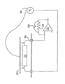
図1Aには、2つのリード(102、104)がプリント回路基板に取り付けられた軸方向リード型電解コンデンサ100の側面図が示されている。コンデンサ100は、被試験デバイス(DUT)である。試験の目的は、リード102及び104が適正に接続されているか否かを判別することにある。非接触容量性プローブ110(導電性プレート)が、コンデンサ100の外部ケースの近くに、ただし電気的に接触しないように配置される。プローブ100とコンデンサ100の外部ケースの間には実効キャパシタンスCP(112)が存在する。
【0008】
例示のため、コンデンサ100は導電性ケースを備えており、リード104はコンデンサ100のケースに接続され、リード104が例示のように接続される時、コンデンサ100は正しく実装されたものと仮定する。さらに、リード104が理想電圧源106によって駆動されており、コンデンサのリード102は、理想リード108によって理想共通信号帰線に接続され、電圧VP(114)が、理想電圧測定装置によって容量性プローブで測定されるものと仮定する。理想部品を用い、正しい極性にすれば、VP(114)は、電圧VS(106)と同じであり、コンデンサ100の導電性ケースからキャパシタンス112を介してプレート110に理想的に結合される。これとは対照的に、コンデンサ100が反転されて、コンデンサ100のケースがリード108によって共通信号帰線109に接続される場合、導電性ケースによって、電圧源106に接続されたコンデンサのリードまわりにファラデー・シールドが形成され、電圧はプレート110に結合されない。これが理想システムであると仮定すると、VP(114)がVS(106)に等しい場合、コンデンサ100は正しく実装されており、VP(114)がゼロであれば、コンデンサ100は正しく実装されていないということになる。
【0009】
VS(106)は、AC(正弦)電圧、即ち交番電圧である。VS(106)に適した値の例は、約1KHzの周波数において(これまた実装される可能性のある半導体デバイスのターン・オンを回避するため)0.6Vピーク・ピークである。一般に、大容量部品には低い周波数(例えば、数百ヘルツ)が適し、小容量部品には高い周波数(約10KHzまで)が適する。
【0010】
図1Bは、実部品による図1Aの回路モデルを示す等価回路図である。典型的な試験システムの場合、刺激電圧106及びリード108は、「ベッド・オブ・ネイル」固定具または他の一時的接続方法を用いて接続される。図1Bに示すように、実在のシステムにおける刺激電圧106は有限の電源及び相互接続インピーダンス116を備えている。コンデンサ100が実装されるシステムは、有限並列インピーダンスを備えている。リード108は、有限相互接続インピーダンス120を備えている。電圧測定装置(及びプローブ110と電圧測定装置の間の回路要素)は、有限キャパシタンス122及び抵抗124を備えている。図1Bの刺激側の有限インピーダンス(コンデンサ100のインピーダンスを含めて)の結果としてコンデンサ100のケースにおける電圧は、刺激電圧106の何分の1かである。コンデンサ100のケースが刺激によって駆動されるものと仮定すると、測定される電圧(114)がある所定のしきい値レベルを超えるか、または、VS(106)の所定の何分の1かを超える場合、コンデンサ100は、正しく実装されている。
【0011】
電圧測定値VPは、キャパシタンス122によって固有の影響を受けることになる。キャパシタンス122に対するシステムの影響は、かなりのものである可能性があり、このシステムの影響は変動する可能性がある。例えば、システムの漂遊キャパシタンスは、相対湿度によって変動する可能性がある。従って、システムの漂遊キャパシタンスによって影響されない測定値を利用することが望ましい。
【0012】
図1Cに示すシステムの等価回路図では、図1Cに示す演算増幅器を用いて、電圧の代わりに電流を測定することによって、システム・キャパシタンス122によって生じる容量性電圧分割の効果を低減する実施例である。キャパシタンス112を通る電流が、演算増幅器130によって間接的に測定される。コンデンサ100が正しく取り付けられていれば、コンデンサ100の導電性ケースは、キャパシタンス112を介して比較的大きい電流を結合し、コンデンサ100の取り付けが間違っていれば、コンデンサ100のケースは刺激電圧をシールドするので、比較的小さい電流がキャパシタンスを流れることになる。コンデンサ100のケースが刺激によって駆動されるものと仮定すると、測定電流が所定のしきい値を超えると、コンデンサ100が正しく実装されていることになる。演算増幅器130の反転入力と演算増幅器130の非反転入力の間の電圧が、極めて低い(ほぼゼロ)ので、漂遊キャパシタンス122の両端間における電圧及びキャパシタンス122を通る電流は、ほぼゼロにまで減少する。
【0013】
図1Cの場合、演算増幅器130のフィードバック抵抗器128の両端間で測定される電圧VP2(126)は、フィードバック抵抗器を通る電流の直接的測度であり、キャパシタンス112を通る電流の間接的測度である。代替案として、キャパシタンス112を流れる電流は、増幅器130の出力と共通信号帰線109との間の電圧から間接的に測定することが可能である。増幅器130に対する入力の両端間における電圧がゼロの場合、この代替測定値(図1CにおいてV’P2(132)として表示)がVP2(126)と同じになる点に留意されたい。V’P2(132)は、一般的な基板試験システムにおいてより計測しやすい測定値である。演算増幅器の入力を利用して、外部回路インピーダンスの影響を軽減することは、接続試験用の容量性プローブを備える市販のテスタにおいて用いられる技法である(例えば、前記Crook他の特許参照のこと)。
【0014】
図1Cの実施例は、図1Bの実施例に改良を加えたものである。しかし、それでも実用上の限界がある。コンデンサ100のインピーダンスが、電源インピーダンス116及び共通帰線インピーダンス120に対して極めて小さい(キャパシタンスが大きい)場合、コンデンサ100のケースにおける刺激電圧を分割すると、低くなりすぎて、上記測定が実施不能になる可能性がある。すなわち、コンデンサ100における刺激電圧の電圧VP(114)に対する影響と、ノイズまたは他の可能性のある結合経路による影響を直接的にかつ確実に区別することは不可能である。これは、刺激周波数を低下させて、コンデンサ100のインピーダンスを増すことによって改善することが可能である。しかし、一般的な基板試験環境において経験上観測されるように、上述の極性試験実施例は、10マイクロファラッドより小さいコンデンサに最もよく適しているが、10マイクロファラッドよりはるかに大きいコンデンサの場合、後述の図2A及び2Bの実施例のような回路インピーダンス及び交流結合経路に対していっそう適正な補償を可能にする極性試験が必要とされる。
【0015】
図2Aにおける容量性プローブ200が被試験デバイスの各リードに対する結合を保証するのに十分な大きさである点を除けば、図2Aは、図1Aと同様の構成の概略図である。図1Aのリード102は、図2A及び図2Bにおいて端子「A」として表示され、添え字「A」のついた値は、端子「A」に関連した刺激または測定値を表示している。図1Aのリード104は、図2A及び2Bにおいて端子「B」として表示され、添え字「B」のついた値は、端子「B」に関連した刺激または測定値を表示している。試験中、第2のリードがVREF(202)に接続されている間に(図2Aに示されるように)、DUTの第1のリードが刺激され、第1のリードがVREF(202)に接続されている間に(図2Bに示すように)、第2のリードが刺激される。
【0016】
図2A及び図2Bの電圧測定値は、全て、基準電圧VREF(202)に対して計測されるが、一般には、VREF(202)と既知の関係を有する他の低ノイズ基準電位に対して計測することが可能である。VREF(202)は大地電位とすることもできるし、あるいは、大地電位以外の電圧とすることも可能である。例えば、DUTの端子の1つが、電子アセンブリのためのアースに接続される場合、基板試験システムは、電子アセンブリを絶縁するか電子アセンブリの電位以外のある電位に浮遊することが必要になる可能性がある。基板試験の分野において、接地電圧または基準電圧は、ガード電圧と呼ばれる場合もある。
【0017】
RSは、刺激106の全電源インピーダンス(刺激とDUTにおけるアクセス可能な測定ポイントとの間の任意の相互接続インピーダンスと組み合わせられる固有の出力電源インピーダンスを含む)である。図1Cに関連して上述のように、コンデンサ100のインピーダンスは、RS(116)に対して小さい場合、コンデンサ100の端子102または104には、VS(106)のほんの一部だけしか生じない。図2A及び2Bに示す実施例の場合、電源インピーダンス及び測定インピーダンスの影響は、端子102及び104において電圧を直接測定することによって最小限に抑えられる。電圧VA1(208)は、物理的に端子「A」の近くにある独立した接触プローブによって端子「A」において測定される。同様に、電圧VB1(210)は、物理的に端子「B」の近くにある独立した接触プローブによって端子「B」において測定される。独立したワイヤによって、DUTのリードに実際に生じる電圧の出来うる最も正確な測定が可能になる。
【0018】
第3の電圧測定値VP1(212)が容量性プローブ200によって計測される。測定電圧VP1(212)は、演算増幅回路130のフィードバック抵抗器128の両端間における電圧であり、DUTのリード及び本体からプローブ200を介して容量結合される電流の和によって決まる。代替案として、VREF(202)に対する増幅器130の出力から第3の測定値を計測することも可能である。図1Cに関して既述のように、この代替測定値(図2AにおけるV’P1及び図2BにおけるV’P2)は、典型的な基板試験システムにおいてより計測しやすい測定値である。
【0019】
電磁結合は、図2A及び2Bに2つのコンデンサとして示されているが、理解しておくべきは、「KA(214)及びKB(216)は、キャパシタンス値ではなく、下記の式によって定義されるように、導電性プレートを流れ、最終的には、演算増幅器に測定電圧を生じる電流に対するDUTリード(及びリードの1つに取り付けられたコンデンサの導電性ケース)における電圧の影響を表す式における無次元数(電磁結合係数)である」という点である:
式1: KAVA1+KBVB1=VP1
【0020】
式1においては、VA1、VB1、及び、VP1は、全て、測定値であるが、電磁結合係数KA及びKBは、両方とも未知であるという点に留意されたい。電磁結合係数KA及びKBを求めるためにはもう1つの式(及び測定の組)が必要がある。図2Bには、DUTの端子「B」を駆動する刺激VS(106)と基準電圧(202)に接続された端子「A」を備えた1組の測定が示されている。端子「A」における電圧(VA2(218))、端子「B」における電圧(VB2(220))、及び、プローブ電流(VP2(222)として測定される)の2度目の測定が行われる。容量性プローブ200がこの2回の測定に関して同じ状態に保たれるので、電磁結合係数は不変である。電源インピーダンス(116、117)及び相互接続インピーダンス(206、207)は、該2回の測定に関して同じではない可能性があるという点に留意されたい。必須電圧はDUTの端子において直接測定されるので、これらのインピーダンスが電磁結合係数の式に影響することはない。第2の組をなす測定電圧及び電磁結合係数は、下記の式によって関連づけられる:
式2: KAVA2+KBVB2=VP2
【0021】
2組の測定の後、式1及び式2を解いて、2つの未知の電磁結合係数KA及びKBが求められる。一般的な基板試験システムがコンピュータ制御式であり(不図示)、該コンピュータを用いて、下記のように2つの未知の係数を持つ2つの線形方程式の周知の問題を解くことが可能である。
式3: KA=(VB1VP2−VB2VP1)/(VB1VA2−V B2 V A1 )
式4: KB=(VA1VP2−VA2VP1)/(VA1VB2−V A2 V B1 )
【0022】
例えば、端子A(102)が導電性ケースに接続される場合、KAの値はKBの値より大きいことが望ましい。KAの値がKBの値より大きいと判定された場合、コンデンサは正しく実装されている。KAの値がKBの値より小さいと判定された場合、コンデンサは逆向きに実装されてる。上述の2ステップの試験が、回路インピーダンスを適切に取り扱い(電圧がDUTの端子において測定される)、非接触プローブに対する交流結合経路(KA及びKB)が適切に取り扱われ、、該試験が単一の絶対測定値ではなく2つの異なる刺激条件における電圧差に依存している点に留意されたい。この2ステップの極性測定は、どんなサイズのコンデンサにも適しており、従って、上記単一ステップの測定のどれよりも用途が広い。
【0023】
図1A〜図1C及び図2A〜図2Bに示す試験構成を逆にして、刺激によってプローブが駆動され、コンデンサのリードにおける電圧が、基準電圧に接続されるリードを交代して測定されるようにすることも可能である。例えば、図3の場合、電圧源106によってプローブ200が駆動され、最初の測定時に、リードBからの電流が共通信号帰線(または基準電圧)に接続されたリードAによって測定される。第2の実施例の場合、リードAからの電流が共通信号帰線(または基準電圧)に接続されたリードBによって測定される。さらに理解しておくべきは、図1A〜1C、図2A〜B、及び、図3に示す電圧刺激106の代わりにテブナン等価電流源を用いることも可能という点である。
【0024】
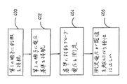
図4は、図1Bの等価回路に関連して既述の第1の実施例に関する構成の1つ(刺激によってDUTを駆動する)を説明するためのフローチャートである。図5は、図1Cの回路に関連して既述の第2の実施例に関する構成の1つ(刺激によってDUTを駆動する)を説明するためのフローチャートである。図6は、図2A及び図2Bの回路に関連して既述の第3の実施例に関する構成の1つ(刺激によってDUTを駆動する)を説明するためのフローチャートである。
【0025】
前記単一ステップ及び2ステップの極性試験では、いずれの場合も、試験システムにはDUTのどのリードがケースに接続されているかわかっている、と仮定している。これは、業者によって変わる可能性があるので、一般には、期待される極性は業者及び部品番号に固有のものならざるをえない。
【0026】
図1Aのコンデンサ100は、特に軸方向リード・コンデンサとして特定されている。上述の試験は、径方向リード電解コンデンサにも適している。一般的な要件は、リードの1つをファラデー・シールドに接続して、電磁結合を非対称にしなければならないということである。すなわち、径方向リード・コンデンサのリードの1つが導電性ケースに取り付けられる場合、あるいは、リードの1つが常にケースに対してより大きい容量で結合するように構成されている場合、上述の単一ステップと2ステップ試験のいずれかを適用することが可能になる。プローブ110または200は、導電性ケースの近くに配置される。両方のリードとも、径方向リード・デバイスにおけるケースによって包囲されているので、リードからの結合はほとんどなく、ケースだけからの結合によって、有効な試験が可能になる。
【0027】
さらに、コンデンサのタイプによっては、コンデンサのリードの1つが導電性ケースに取り付けられていなくても、あるいは、コンデンサ本体の外表面が導電性でなくても、上述の極性試験がおこなえる。例えば、表面実装タンタル・コンデンサが、技術的に独立した導電性ケースを備えることができなくても、上述の極性試験を表面実装タンタル・コンデンサに利用することが可能である。表面実装タンタル・コンデンサは、一般に固体電解質を包囲する多孔性金属外壁を備えている。一般に、この多孔性金属外壁によって、上述の極性試験を可能にするのに十分な非対称結合(ファラデー・シールド)が得られる。さらに、コンデンサが導体及び誘電体を円筒状に巻いた層から構成される場合、最も外側の層によって、導電性ケースと同じ非対称結合(ファラデー・シールド)が得られる。従って、特定のコンデンサ構造によって、必ず外側導電層と同じ導体が得られる場合、上述の極性試験を利用することが可能である。
【0028】
本発明の以上の説明は、例示及び解説を目的として提示されたものである。余すところなく述べようとしたり、あるいは、本発明を開示のそのままの形態に限定しようとしたりするものではなく、上述の教示に照らして他の修正及び変更を加えることも可能である。該実施例は、本発明の原理及びその実際の適用例について最も明確に説明し、当該技術の他の熟練者が、特定の企図する用途に適したさまざまな具現化及びさまざまな修正において本発明を最も有効に活用できるようにするため、選択され、解説されたものである。付属の請求項は、先行技術による制限のない限り、本発明の他の代替実施例を含むものと解釈されるものとする。
【図面の簡単な説明】
【図1A】プリント回路基板における軸方向リード電解コンデンサの極性を検出するための回路の側面概略図である。
【図1B】図1Aのシステムの等価回路図である。
【図1C】測定回路が改良された、図1Aのシステムの等価回路図である。
【図2A】被試験デバイス並びに関連する刺激及び応答回路要素、及び、最初の測定に関する変数の定義を示す、コンデンサの極性検出回路の回路図である。
【図2B】第2の測定に関する変数の定義と共に、図2Aの被試験デバイスを示す概略図である。
【図3】刺激がプローブに接続される代替試験構成を示すコンデンサ極性検出回路の側面部分概略図である。
【図4】第1の実施例の構成の1つに関する方法のフローチャートである。
【図5】第2の実施例の構成の1つに関する方法のフローチャートである。
【図6】第3の実施例の構成の1つに関する方法のフローチャートである。
【符号の説明】
100 コンデンサ
102 リード
104 リード
106 電圧源
108 リード
109 共通信号帰線
110 プローブ
128 フィードバック抵抗器
130 演算増幅器
200 容量性プローブ[0001]
[Industrial applications]
The present invention generally relates to discriminating electronic assemblies, and more particularly to discriminating polarity for determining whether a polar component is mounted with the correct polarity or a predetermined polarity.
[0002]
BACKGROUND OF THE INVENTION
In the electronic manufacturing test and the failure test, it is a current problem to automatically determine whether a polarized component is mounted with an appropriate polarity. Electrolytic capacitors, diodes, integrated circuits, and other devices are mechanically symmetric but often electrically asymmetric. That is, they can be physically mounted or mounted in any one of several orientations, but only properly when mounted or mounted in a particular orientation. Cannot work.
[0003]
Electrolytic capacitors are particularly problematic when mounted with their terminals reversed, because they can function for a period of time. As a result, electrolytic capacitors may pass typical conventional circuit testing at the time of manufacture, but may degrade over time, have increased leakage current, or have catastrophic failure at a later time. (Explosion). The need to detect degraded devices is economically important, as repairing a product before final assembly is much less expensive than repairing the shipped product. For potentially explosive devices, it is particularly important to determine the mounting polarity before the full operating voltage is applied for the first time, both from a safety and cost standpoint. There is a need for an automatic test for the polarity of the capacitor, and in particular, an automatic test using equipment already provided for testing other components of the electronic assembly.
[0004]
Many commercially available testers for mounted printed circuit boards have two types of probes for applying an electronic stimulus signal and measuring the electronic response. The contact probe makes physical contact with a conductive surface in the electronic assembly. Generally, a pointed "nail" is used to pierce the protective coating and make contact with traces or pads on the printed circuit board. A non-contact probe induces or measures an electromagnetic field near the electronic device under test. For example, the use of a non-contact capacitive probe is used to detect open solder joints on a mounted printed circuit board. An example of a commercially available printed circuit board tester utilizing the "Bed of Nail" fixture and a non-contact probe is the Hewlett-Packard 3070 Series II test with a non-contact probe called HP TestJet. There is a system. David T. on October 19, 1993. Crook and Kevin W.W. U.S. Pat. No. 5,254,953 issued to Keirn (Crook et al.) Provides an example of non-contact testing utilized in integrated circuits. There is a need to automatically test the polarity of assembled electronics using existing test probe hardware such as "bed of nail" probes and non-contact probes.
[0005]
Summary of the Invention
In the description of the present invention, the polar component is represented by an electrolytic capacitor, and the polarity of the electrolytic capacitor is determined by measuring the electromagnetic coupling between the capacitor and the non-contact probe. In one configuration, the device under test is actively stimulated and the response is detected by a non-contact capacitive probe located near the body of the device under test. Alternatively, the probe may be stimulated and measured at the lead of the device under test, separately from stimulating the lead of the device under test and measuring with the probe.
[0006]
In the case of the first embodiment, a single voltage measurement is performed. In the case of the second embodiment, a single current measurement is performed. In the case of the third embodiment, multiple voltage and current measurements are performed in two different test configurations. In the case of the third embodiment, the two electromagnetic coupling coefficients are unknown fixed coefficients in the two linear equations. The variable parameters in the two linear equations are the voltage at each terminal of the device under test and the current flowing through the capacitive probe. In the first configuration of the third embodiment, the first terminal of the device under test is stimulated and the second terminal is held at the reference voltage (or connected to a common signal return). In the case of the second configuration of the third embodiment, the first terminal is held at the reference voltage (or connected to the common signal return) and the second terminal is stimulated. After measuring the four terminal voltages and the two probe currents, the two equations are solved to determine the unknown electromagnetic coupling coefficient. The relative relationship between the electromagnetic coupling coefficients determines the measured polarity of the device under test.
[0007]
【Example】
FIG. 1A shows a side view of an axial lead
[0008]
For purposes of illustration,
[0009]
V S (106) is an AC (sine) voltage, that is, an alternating voltage. Examples of values appropriate to V S (106) is a (also for avoiding the turn-on of the semiconductor devices that may be implemented) 0.6V peak-to-peak at a frequency of about 1 KHz. Generally, low frequencies (eg, several hundred hertz) are suitable for large capacity components, and high frequencies (up to about 10 KHz) are suitable for small capacity components.
[0010]
FIG. 1B is an equivalent circuit diagram showing the circuit model of FIG. 1A using actual components. In a typical test system, the
[0011]
Voltage measurements V P will experience a unique influence by the
[0012]
The equivalent circuit diagram of the system shown in FIG. 1C illustrates an embodiment in which the operational amplifier shown in FIG. 1C is used to measure current instead of voltage, thereby reducing the effect of capacitive voltage division caused by
[0013]
In the case of FIG. 1C, the voltage VP2 (126) measured across the
[0014]
The embodiment of FIG. 1C is an improvement of the embodiment of FIG. 1B. However, there are still practical limitations. If the impedance of the
[0015]
FIG. 2A is a schematic diagram of a configuration similar to FIG. 1A, except that the
[0016]
The voltage measurements in FIGS . 2A and 2B are all measured with respect to the reference voltage V REF (202), but generally with respect to other low noise reference potentials having a known relationship with V REF (202). It is possible to measure. V REF (202) can be at ground potential or at a voltage other than ground potential. For example, one of the terminals of the DUT, when connected to the ground for electronic assemblies, board test system can require you to float to a potential other than the potential of either the electronic assembly to insulate the electronic assembly There is. In the field of substrate testing, a ground voltage or a reference voltage is sometimes called a guard voltage.
[0017]
RS is the total power supply impedance of the
[0018]
A third voltage measurement VP1 (212) is measured by the
[0019]
Although the electromagnetic coupling is shown in FIGS. 2A and 2B as two capacitors, it should be understood that "K A (214) and K B (216) are not capacitance values, but are defined by the following equations: Equation describing the effect of the voltage on the DUT lead (and the conductive case of the capacitor attached to one of the leads) on the current flowing through the conductive plate and ultimately yielding the measured voltage in the operational amplifier Is the dimensionless number (electromagnetic coupling coefficient) in
Equation 1: K A V A1 + K B V B1 = V P1
[0020]
Note that in Equation 1, V A1 , V B1 , and V P1 are all measured values, but the electromagnetic coupling coefficients K A and K B are both unknown. Another formula for determining the electromagnetic coupling coefficient K A and K B are (and the set of measurement) must. FIG. 2B shows a set of measurements with stimulus V S (106) driving terminal “B” of the DUT and terminal “A” connected to reference voltage (202). A second measurement of the voltage at terminal “A” (V A2 (218)), the voltage at terminal “B” (V B2 (220)), and the probe current (measured as V P2 (222)) is performed. Is Since the
Equation 2: K A V A2 + K B V B2 = V P2
[0021]
After two sets of measurements, by solving the equations 1 and 2, two unknown electromagnetic coupling coefficient K A and K B are determined. Common substrates trial silk thread stem is computer controlled (not shown), using the computer, can be solved well-known problem of two linear equations with two unknown coefficients as follows is there.
Formula 3: K A = (V B1 V P2 −V B2 V P1 ) / (V B1 V A2 −V B2 V A1 )
Equation 4: KB = (V A1 V P2 -V A2 V P1) / (V A1 V B2 - V A2 V B1 )
[0022]
For example, when the terminal A (102) is connected to the conductive case, the value of K A is preferably larger than the value of K B. If the value of K A is determined to be greater than the value of K B, the capacitor is implemented correctly. If the value of K A is determined to be smaller than the value of K B, the capacitor is mounted in the opposite direction. The two-step test described above properly handles the circuit impedance (voltage is measured at the terminals of the DUT), the AC coupling paths (K A and K B ) for the contactless probe are properly handled, and Note that it relies on a voltage difference at two different stimulation conditions rather than a single absolute measurement. This two-step polarity measurement is suitable for capacitors of any size and is therefore more versatile than any of the single-step measurements described above.
[0023]
1A-1C and FIGS. 2A-2B are reversed so that the stimulus drives the probe and the voltage at the capacitor leads is measured alternately with the leads connected to the reference voltage. It is also possible. For example, in the case of FIG. 3, the
[0024]
FIG. 4 is a flowchart for explaining one of the configurations (driving the DUT by stimulus) related to the first embodiment described above in relation to the equivalent circuit of FIG. 1B. FIG. 5 is a flowchart for explaining one configuration (driving a DUT by a stimulus) relating to the second embodiment described above with reference to the circuit of FIG. 1C. FIG. 6 is a flowchart for explaining one of the configurations (the DUT is driven by the stimulus) according to the third embodiment described above with reference to the circuits of FIGS. 2A and 2B.
[0025]
The single-step and two-step polarity tests assume in each case that the test system knows which leads of the DUT are connected to the case. Since this can vary from vendor to vendor, generally the expected polarity must be vendor and part number specific.
[0026]
1A is specifically identified as an axial lead capacitor. The above test is also suitable for radial lead electrolytic capacitors. A general requirement is that one of the leads must be connected to the Faraday shield to make the electromagnetic coupling asymmetric. That is, if one of the leads of the radial lead capacitor is attached to the conductive case, or if one of the leads is always configured to couple with a larger capacitance to the case, the above-described single step And one of the two-step tests can be applied. The
[0027]
Further, depending on the type of capacitor, the polarity test described above can be performed even if one of the capacitor leads is not attached to the conductive case or the outer surface of the capacitor body is not conductive. For example, the polarity test described above can be used for surface mount tantalum capacitors, even if the surface mount tantalum capacitor cannot have a technically independent conductive case. Surface mount tantalum capacitors generally have a porous metal outer wall surrounding a solid electrolyte. Generally, this porous metal outer wall provides sufficient asymmetric coupling (Faraday shield) to allow for the polarity test described above. Furthermore, if the capacitor is composed of layers of conductors and dielectrics rolled into a cylinder, the outermost layer provides the same asymmetric coupling (Faraday shield) as the conductive case. Thus, if a particular capacitor structure always results in the same conductor as the outer conductive layer, the polarity test described above can be used.
[0028]
The foregoing description of the present invention has been presented for purposes of illustration and description. It is not intended to be exhaustive or to limit the invention to the precise form disclosed, and other modifications and changes may be made in light of the above teachings. The embodiments most clearly explain the principles of the present invention and its practical applications, and others skilled in the art will appreciate that Are selected and explained in order to make the most effective use of It is intended that the appended claims be construed to include other alternative embodiments of the invention unless limited by the prior art.
[Brief description of the drawings]
1A is a schematic side view of a circuit for detecting the polarity of an axial lead electrolytic capacitor on a printed circuit board. FIG.
FIG. 1B is an equivalent circuit diagram of the system of FIG. 1A.
FIG. 1C is an equivalent circuit diagram of the system of FIG. 1A with an improved measurement circuit.
FIG. 2A is a circuit diagram of a capacitor polarity detection circuit showing the device under test and associated stimulus and response circuitry, and the definition of variables for the first measurement.
FIG. 2B is a schematic diagram showing the device under test of FIG. 2A with definitions of variables for a second measurement.
FIG. 3 is a side schematic view of a capacitor polarity detection circuit showing an alternative test configuration in which a stimulus is connected to a probe.
FIG. 4 is a flowchart of a method for one of the configurations of the first embodiment.
FIG. 5 is a flowchart of a method for one of the configurations of the second embodiment.
FIG. 6 is a flowchart of a method for one of the configurations of the third embodiment.
[Explanation of symbols]
REFERENCE SIGNS
Claims (7)
(a)プローブを前記第1、第2の端子の近くに、ただし電気的に接触しないように配置するステップと、
(b)前記プローブと前記第1の端子間の第1の電磁結合係数及び前記プローブと前記第2の端子間の第2の電磁結合係数とを測定するステップと、
(c)前記第1の電磁結合係数が前記第2の電磁結合係数の大きさを超える場合、前記コンデンサが所定の極性であると決定するステップとを備える実装部品の極性判別方法。A method for determining whether a capacitor in an electronic assembly, having first and second terminals and driven by a stimulus, is implemented with a predetermined polarity.
(A) arranging a probe near the first and second terminals but not in electrical contact;
(B) measuring a second electromagnetic coupling coefficient between the first electromagnetic coupling coefficient and the said probe second terminals between the said probe first terminal,
(C) determining that the capacitor has a predetermined polarity when the first electromagnetic coupling coefficient exceeds the magnitude of the second electromagnetic coupling coefficient.
(b1)刺激によって前記第1の端子を駆動するステップと、
(b2)前記第2の端子を基準電圧に接続するステップと、
(b3)前記第1の端子が前記刺激によって駆動されている間、及び、前記第2の端子が前記基準電圧に接続されている間に、
(b3a)前記第1の端子における第1の電圧の測定、
(b3b)前記第2の端子における第2の電圧の測定、及び
(b3c)前記プローブを通る第1の電流の測定、
を実施するステップと、
(b4)前記刺激によって前記第2の端子を駆動するステップと、
(b5)前記第1の端子を前記基準電圧に接続するステップと、
(b6)第2の端子が前記刺激によって駆動されて且つ前記第1の端子が前記基準電圧に接続されている間に、
(b6a)前記第1の端子における第3の電圧の測定、
(b6b)前記第2の端子における第4の電圧の測定、及び
(b6c)前記プローブを通る第2の電流の測定、
を実施するステップと、
(b7)前記測定により得られた前記第1〜第4の電圧及び前記第1、第2の電流を利用して、前記第1、第2の電磁結合係数を計算するステップ、
とを備える請求項1に記載の実装部品の極性判別方法。The step (b) further comprises:
(B1) driving the first terminal with a stimulus;
(B2) connecting the second terminal to a reference voltage;
(B3) while the first terminal is driven by the stimulus, and while the second terminal is connected to the reference voltage,
(B3a) measuring a first voltage at the first terminal;
(B3b) measuring a second voltage at the second terminal, and (b3c) measuring a first current through the probe;
Performing
(B4) driving the second terminal by the stimulus;
(B5) connecting the first terminal to the reference voltage;
(B6) while a second terminal is driven by the stimulus and the first terminal is connected to the reference voltage,
(B6a) measuring a third voltage at the first terminal;
(B6b) measuring a fourth voltage at the second terminal, and (b6c) measuring a second current through the probe;
Performing
(B7) calculating the first and second electromagnetic coupling coefficients using the first to fourth voltages and the first and second currents obtained by the measurement;
2. The method according to claim 1, further comprising the steps of:
(b1)刺激によって前記プローブを駆動するステップと、
(b2)前記第2の端子を基準電圧に接続するステップと、
(b3)前記プローブが前記刺激によって駆動され前記第2の端子が前記基準電圧に接続されている間に、
(b3a)前記第1の端子における第1の電圧の測定、
(b3b)前記第2の端子における第2の電圧の測定、及び
(b3c)前記第1の端子を通る第1の電流の測定、
を実施するステップと、
(b4)前記第1の端子を前記基準電圧に接続するステップと、
(b5)前記第1の端子が前記基準電圧に接続されている間に、
(b5a)前記第1の端子における第3の電圧の測定、
(b5b)前記第2の端子における第4の電圧の測定、及び
(b5c)前記第2の端子を通る第2の電流の測定、
を実施するステップと、
(b6)前記測定により得られた前記第1〜第4の電圧及び前記第1、第2の電流を利用して前記第1、第2の電磁結合係数を計算するステップとを備える請求項1に記載の実装部品の極性判別方法。Step (b) further comprises:
(B1) driving the probe with a stimulus;
(B2) connecting the second terminal to a reference voltage;
(B3) while the probe is driven by the stimulus and the second terminal is connected to the reference voltage,
(B3a) measuring a first voltage at the first terminal;
(B3b) measuring a second voltage at the second terminal, and (b3c) measuring a first current passing through the first terminal.
Performing
(B4) connecting the first terminal to the reference voltage;
(B5) While the first terminal is connected to the reference voltage,
(B5a) measuring a third voltage at the first terminal;
(B5b) measuring a fourth voltage at the second terminal, and (b5c) measuring a second current passing through the second terminal.
Performing
(B6) calculating the first and second electromagnetic coupling coefficients using the first to fourth voltages and the first and second currents obtained by the measurement. 4. A method for determining the polarity of a mounted component according to item 1.
Applications Claiming Priority (2)
| Application Number | Priority Date | Filing Date | Title |
|---|---|---|---|
| US37261995A | 1995-01-11 | 1995-01-11 | |
| US372,619 | 1995-01-11 |
Publications (2)
| Publication Number | Publication Date |
|---|---|
| JPH08233894A JPH08233894A (en) | 1996-09-13 |
| JP3574708B2 true JP3574708B2 (en) | 2004-10-06 |
Family
ID=23468939
Family Applications (1)
| Application Number | Title | Priority Date | Filing Date |
|---|---|---|---|
| JP35363495A Expired - Fee Related JP3574708B2 (en) | 1995-01-11 | 1995-12-29 | How to determine the polarity of mounted components |
Country Status (4)
| Country | Link |
|---|---|
| US (1) | US6169395B1 (en) |
| EP (1) | EP0722091B1 (en) |
| JP (1) | JP3574708B2 (en) |
| DE (1) | DE69532626T2 (en) |
Families Citing this family (15)
| Publication number | Priority date | Publication date | Assignee | Title |
|---|---|---|---|---|
| US5844412A (en) * | 1996-12-19 | 1998-12-01 | Teradyne, Inc. | Board test apparatus and method for fast capacitance measurement |
| GB2337337B (en) * | 1998-05-12 | 2002-03-06 | Ifr Ltd | Apparatus for and method of determining the polarity of a capacitor |
| JP4490005B2 (en) * | 2001-08-08 | 2010-06-23 | 株式会社日立製作所 | Printed circuit board test method and test apparatus |
| US6798213B2 (en) | 2002-07-30 | 2004-09-28 | Oes, Inc. | Circuit analyzer with component testing capability |
| CN100409016C (en) * | 2003-09-04 | 2008-08-06 | 系新科技股份有限公司 | Method and apparatus for testing capacitor of printed circuitboard |
| US7212011B2 (en) * | 2004-06-30 | 2007-05-01 | Matsushita Electrid Industrial Co. Ltd. | Capacitor deterioration judgment method |
| TW200719135A (en) * | 2005-11-03 | 2007-05-16 | Inventec Corp | Method and system for automatically inspecting polarity installation direction of a capacitor |
| JP4969130B2 (en) * | 2006-03-29 | 2012-07-04 | 協立電機株式会社 | Mounted component polarity discrimination device |
| US8253425B2 (en) * | 2007-05-08 | 2012-08-28 | Synaptics Incorporated | Production testing of a capacitive touch sensing device |
| US8179143B2 (en) * | 2008-10-15 | 2012-05-15 | Test Research, Inc. | Apparatus for testing printed circuit and method therefor |
| US20130234749A1 (en) * | 2010-11-10 | 2013-09-12 | Tokyo Electronics Trading Co., Ltd. | Apparatus for testing immunity of electronic equipment against fluctuating electric field and method for testing immunity of electronic equipment against fluctuating electric field |
| JP6347702B2 (en) * | 2014-09-09 | 2018-06-27 | 日置電機株式会社 | Inspection apparatus and inspection method |
| JP6815169B2 (en) * | 2016-11-07 | 2021-01-20 | Juki株式会社 | Polarity discrimination device, mounting device, polarity discrimination method |
| CN108132406A (en) * | 2017-12-13 | 2018-06-08 | 格力电器(武汉)有限公司 | A kind of electron device testing equipment |
| CN109188161B (en) * | 2018-11-06 | 2020-07-31 | 苏州电器科学研究院股份有限公司 | Capacitor detection equipment and detection method thereof |
Family Cites Families (6)
| Publication number | Priority date | Publication date | Assignee | Title |
|---|---|---|---|---|
| EP0185255B1 (en) * | 1984-12-17 | 1991-11-06 | Siemens Aktiengesellschaft | Method to determine the polarity of electronic components, and arrangement for carrying out this method |
| DE3778455D1 (en) * | 1986-08-01 | 1992-05-27 | Siemens Ag | METHOD AND DEVICE FOR DETECTING THE POLARITY OF POLED CAPACITORS. |
| DE4137758A1 (en) * | 1991-11-16 | 1993-05-19 | Bosch Gmbh Robert | METHOD AND DEVICE FOR CHECKING THE POLARITY OF ELECTROLYTE CAPACITORS |
| US5159526A (en) * | 1991-12-20 | 1992-10-27 | Compaq Computer Corporation | Method and apparatus for determining orientation of polarized capacitors |
| KR940007718B1 (en) * | 1992-12-01 | 1994-08-24 | 금성산전 주식회사 | Capacitor reverse inserting detect circuit of in-circuit tester |
| US5502375A (en) * | 1994-08-04 | 1996-03-26 | Compaq Computer Corporation | Method and apparatus for determining orientation of polarized capacitors |
-
1995
- 1995-12-29 JP JP35363495A patent/JP3574708B2/en not_active Expired - Fee Related
- 1995-12-29 DE DE69532626T patent/DE69532626T2/en not_active Expired - Fee Related
- 1995-12-29 EP EP95120740A patent/EP0722091B1/en not_active Expired - Lifetime
-
1997
- 1997-07-16 US US08/903,321 patent/US6169395B1/en not_active Expired - Fee Related
Also Published As
| Publication number | Publication date |
|---|---|
| EP0722091A2 (en) | 1996-07-17 |
| EP0722091B1 (en) | 2004-03-03 |
| EP0722091A3 (en) | 1997-07-16 |
| US6169395B1 (en) | 2001-01-02 |
| DE69532626T2 (en) | 2005-02-10 |
| DE69532626D1 (en) | 2004-04-08 |
| JPH08233894A (en) | 1996-09-13 |
Similar Documents
| Publication | Publication Date | Title |
|---|---|---|
| JP3574708B2 (en) | How to determine the polarity of mounted components | |
| US5254953A (en) | Identification of pin-open faults by capacitive coupling through the integrated circuit package | |
| US5557209A (en) | Identification of pin-open faults by capacitive coupling through the integrated circuit package | |
| JP3228816B2 (en) | Circuit board test apparatus and circuit board test method | |
| US5517110A (en) | Contactless test method and system for testing printed circuit boards | |
| US6097202A (en) | Circuit board inspection apparatus and method | |
| US20070018672A1 (en) | Method and apparatus for engineering a testability interposer for testing sockets and connectors on printed circuit boards | |
| JP3611330B2 (en) | Capacitive open circuit test with improved threshold determination | |
| JP2625623B2 (en) | Circuit test apparatus and method | |
| US7242198B2 (en) | Method for using internal semiconductor junctions to aid in non-contact testing | |
| JP5283707B2 (en) | Electrostatic chuck inspection method and electrostatic chuck apparatus | |
| US5625292A (en) | System for measuring the integrity of an electrical contact | |
| US5969530A (en) | Circuit board inspection apparatus and method employing a rapidly changing electrical parameter signal | |
| KR930700855A (en) | System and method for simultaneously executing electronic device test and lead inspection | |
| US5502375A (en) | Method and apparatus for determining orientation of polarized capacitors | |
| JP2012149914A (en) | Apparatus and method for inspecting degradation of printed wiring board | |
| JP5231295B2 (en) | Inspection apparatus and inspection method thereof | |
| CN100368762C (en) | Conductor inspecting device and conductor inspecting method | |
| JP3599929B2 (en) | Circuit board pattern capacitance measurement method | |
| JP2006200973A (en) | Circuit board inspection method and its device | |
| JP2000232141A (en) | Method for testing conduction of substrate for semiconductor package | |
| TWM549351U (en) | Inspection device for determining quality of conduction pattern | |
| JP3281164B2 (en) | Foot Lift Detection Method Using IC In-Circuit Tester | |
| JP4231682B2 (en) | Bypass capacitor mounting inspection method | |
| KR970022342A (en) | Test device of semiconductor device |
Legal Events
| Date | Code | Title | Description |
|---|---|---|---|
| A977 | Report on retrieval |
Free format text: JAPANESE INTERMEDIATE CODE: A971007 Effective date: 20040213 |
|
| A131 | Notification of reasons for refusal |
Free format text: JAPANESE INTERMEDIATE CODE: A131 Effective date: 20040218 |
|
| A521 | Written amendment |
Free format text: JAPANESE INTERMEDIATE CODE: A523 Effective date: 20040402 |
|
| TRDD | Decision of grant or rejection written | ||
| A01 | Written decision to grant a patent or to grant a registration (utility model) |
Free format text: JAPANESE INTERMEDIATE CODE: A01 Effective date: 20040614 |
|
| A61 | First payment of annual fees (during grant procedure) |
Free format text: JAPANESE INTERMEDIATE CODE: A61 Effective date: 20040705 |
|
| R150 | Certificate of patent or registration of utility model |
Free format text: JAPANESE INTERMEDIATE CODE: R150 |
|
| LAPS | Cancellation because of no payment of annual fees |