JP3556111B2 - Package for electronic component, electronic component assembly using the same, and method of manufacturing electronic component assembly - Google Patents
Package for electronic component, electronic component assembly using the same, and method of manufacturing electronic component assembly Download PDFInfo
- Publication number
- JP3556111B2 JP3556111B2 JP36496898A JP36496898A JP3556111B2 JP 3556111 B2 JP3556111 B2 JP 3556111B2 JP 36496898 A JP36496898 A JP 36496898A JP 36496898 A JP36496898 A JP 36496898A JP 3556111 B2 JP3556111 B2 JP 3556111B2
- Authority
- JP
- Japan
- Prior art keywords
- electrode
- base
- electronic component
- sealing
- grounding
- Prior art date
- Legal status (The legal status is an assumption and is not a legal conclusion. Google has not performed a legal analysis and makes no representation as to the accuracy of the status listed.)
- Expired - Fee Related
Links
Images


Description
【0001】
【発明の属する技術分野】
本発明は、水晶振動素子、水晶発振素子、SAWデバイス素子等の電子素子を収納する電子部品用パッケージに関する。
本発明はまた、前記の電子部品用パッケージに電子素子を組み付けた電子部品中間構体を、プリント基板等の取付基板に組み付けた電子部品組立構体に関する。
本発明はさらに、前記電子部品組立構体の製造方法に関する。
【0002】
【従来の技術】
水晶振動子、水晶発振子、SAWデバイス用の気密パッケージとして、絶縁性ベースと、この絶縁性ベースの内方から絶縁性ベースの外方に導出された電極と、絶縁性ベースの開口部に封止材を介して気密に封止されたキャップとを有する気密パッケージがある。そのような気密パッケージは、水晶振動素子等の形状により各種のものがある。例えば、矩形板状の水晶振動素子用の気密パッケージとしては、実開平6−77328号公報に開示されているものがある。その典型的なものについて、以下説明する。
図11は従来の気密パッケージの斜視図で、図12はその封止材およびキャップの一部を除去した平面図、図13は図12のB−B線に沿う縦断面図である。
図11ないし図13において、71はアルミナセラミツク製の箱状の絶縁製ベースで、底板部72および枠体部73を有する。74、75は絶縁製ベース71の内方から外方に導出された銀パラジウムペースト等の塗布・焼成により形成された電極、76は前記電極74、75と同一材料で同時に形成された、後述する水晶振動素子等の電子素子を支持する、いわゆる「枕」と称される支持部である。2点鎖線で示す77は前記電極74、75に導電性接着材により接続固定された水晶振動素子等の電子素子、78は前記絶縁性ベース71の開口部を封止する封止材で、絶縁性ベース71の枠体部73の上面とアルミナセラミック製のキャップ79の下面とを封止している。
上記構成の気密パッケージにおいては、キャップ79としてアルミナセラミック等の絶縁性キャップを用いているため、機械的強度の点からその厚さ寸法t2の薄型化に限度があり、それに伴って気密パッケージ全体の厚さ寸法t3の薄型化にも限度がある。また、浮遊容量や外来電磁波に起因する電子素子7の特性変動を防止できない。
このため、アルミナセラミツク製の絶縁性キャップ79に代えて金属キャップを用いることも考えられている。しかしながら、アルミナセラミック製の絶縁性ベース71に金属キャップを組み合わすことは、両者の熱膨張係数差による応力で、封止材78に亀裂が生じたり、金属キャップが剥離するという問題がある。
そこで、アルミナセラミック製の絶縁性ベース71の枠体部73の上に、絶縁性ベース71と金属キャップとの中間の熱膨張係数の中間金属枠体部を介在することも考えられている。しかしながら、このような構成では、中間金属枠体部が必要になり、材料費および加工費が嵩むのみならず、気密パッケージ全体が嵩高になり、低背化にも反する。
【0003】
そこで、本出願人は、ガラス中にフォルステライト粉末を30〜70wt%混入した熱膨張係数が10〜15×10−6/℃のガラスセラミツクからなる絶縁性ベースを開発するとともに、この絶縁性ベースにこれと近似する熱膨張係数金属を有するステンレス鋼よりなる金属キャップを封止材で封止する気密パッケージを提案した。このような構成の気密パツケージによれば、絶縁性ベースと金属キャップとの熱膨張係数が近似しているので、熱膨張係数差に起因する応力発生がなく、電子素子の特性変動が生じない気密パツケージが提供できる。また、金属キャップを接地すれば、浮遊容量や外来電磁波に起因する電子素子の特性変動も生じない。
なお、上記の絶縁性ベース71を用いて電子素子77を気密に封止した気密パッケージを用いた電子部品およびその電子部品をプリント基板等の取付基板に組み付けた電子部品組立構体の製造方法を、図14の製造工程ブロック図に示す。まず、絶縁性ベース71を製作し(図14a)。次に、この絶縁性ベース71の電極74、75に電子素子77を組み付けて電子部品中間構体を製作する(図14b)。次に、絶縁ベース71の開口部を金属キャップで封止して電子部品を製作する(図14c)。そして、前記電子部品をその下面に形成した電極74、75を利用して、プリント基板等の取付基板に組み付けて電子部品組立構体を製造する(図14d)。
【0004】
【発明が解決しようとする課題】
しかしながら、上記の構成の気密パツケージにおいても、金属キャップが必要で、気密パッケージ全体の低背化には限度があり、しかもこの金属キャップを絶縁性ベースの枠体部に封止材を介して気密に封止する必要があるため、キャップの封止と、電子部品の取付基板への組み付けと、二度の加熱工程が必要になり、電子素子77の加熱に伴う特性変動が生じやすい。
そこで、本発明は、上記の気密パツケージ用からキャップを省略し得る電子部品用パッケージを提供することを目的とする。
本発明はまた、上記の電子部品用パツケージを用いた電子部品組立構体を提供することを目的とする。
本発明はさらにまた、電子部品用パツケージを用いた電子部品組立構体の製造方法を提供することを目的とする。
【0005】
【課題を解決するための手段】
本発明は、底板部および枠体部とを有するベースと、このベースの内方からベースの外方に導出され前記枠体部の端面部を通って枠体部の上面部まで形成された電子素子用電極と、前記ベースの枠体部の上面部に前記電子素子用電極と離隔して形成された接地兼封止用電極とを有する電子部品用パツケージである。
本発明はまた、底板部および枠体部とを有するベースと、このベースの内方からベースの外方に導出され前記枠体部の端面部を通って枠体部の上面部まで形成された電子素子用電極と、前記ベースの枠体部の上面部に前記電子素子用電極と離隔して形成された接地兼封止用電極と、前記接地兼封止用電極に被着された封止材とを有する電子部品用パツケージにおける前記電子素子用電極に電子素子を接続固着してなる電子部品中間構体を、前記電子素子用電極を取付基板の回路端子に接続するとともに、前記封止材で取付基板に気密に固着封止した電子部品組立構体である。
本発明はさらに、底板部および枠体部とを有するベースと、このベースの内方からベースの外方に導出され前記枠体部の端面部を通って枠体部の上面部まで形成された電子素子用電極と、前記ベースの枠体部の上面部に前記電子素子用電極と離隔して形成された接地兼封止用電極と、前記接地兼封止用電極に被着された導電性封止材とを有する電子部品用パツケージを用意する工程と、前記電子部品用パツケージにおける電子素子用電極に電子素子を接続固着して電子部品中間構体を製作する工程と、前記電子素子用電極を取付基板の回路端子に接続すると同時に、前記封止材で取付基板に気密に固着封止する工程とを有する電子部品組立構体の製造方法である。
【0006】
【発明の実施の形態】
本発明の請求項1記載の発明は、底板部および枠体部を有するベースと、このベースの内方から外方に導出され前記枠体部の端面部および上面部まで形成された電子素子用電極と、前記枠体部の上面部に前記電子素子用電極と離隔して形成された接地兼封止用電極とを有する電子部品用パッケージである。
【0007】
本発明の請求項2記載の発明は、底板部および枠体部を有するベースと、このベースの内方から外方に導出され前記枠体部の端面部および上面部まで形成された電子素子用電極と、前記枠体部の上面部に前記電子素子用電極と離隔して形成された接地兼封止用電極と、前記接地兼封止用電極に被着された封止材とを有する電子部品用パッケージである。
【0008】
本発明の請求項3記載の発明は、底板部および枠体部を有するベースと、このベースの内方から外方に導出され前記枠体部の端面部および上面部まで形成された電子素子用電極と、前記枠体部の上面部に前記電子素子用電極と離隔して形成された接地兼封止用電極と、前記接地兼封止用電極に被着された導電性封止材とを有する電子部品用パッケージである。
【0009】
本発明の請求項4記載の発明は、底板部および枠体部を有するベースと、このベースの内方から外方に導出され前記枠体部の端面部および上面部まで形成された電子素子用電極と、前記枠体部の上面部に前記電子素子用電極と離隔して枠状に形成された接地兼封止用電極と、前記接地兼封止用電極に被着されたはんだよりなる導電性封止材とを有する電子部品用パッケージである。
【0010】
本発明の請求項5記載の発明は、底板部および枠体部を有するベースと、このベースの内方から外方に導出され前記枠体部の端面部および上面部まで形成された電極と、前記枠体部の上面部に前記電子素子用電極と離隔して枠状に形成された接地兼封止用電極と、前記接地兼封止用電極に被着された導電性封止材とを有する電子部品用パッケージにおける、前記電子素子用電極に電子素子を接続固着した電子部品中間構体を、その開口部をキャップで封止することなく、前記電子素子用電極を取付基板の回路端子に電気的に接続するとともに、前記接地兼封止用電極を前記取付基板に前記封止材で気密に固着封止したことを特徴とする電子部品組立構体である。
【0011】
本発明の請求項6記載の発明は、底板部および枠体部を有するベースと、このベースの内方から外方に導出され前記枠体部の端面部および上面部まで形成された電子素子用電極と、前記枠体部の上面部に電子素子用電極と離隔して枠状に形成された接地兼封止用電極と、前記接地兼封止用電極に被着された導電性封止材とを有する電子部品用パッケージにおける、前記電子素子用電極に電子素子を接続固着した臀部品中間構体を、キャップで封止することなく、前記電子素子用電極を取付基板の回路電極に電気的に接続するとともに、前記接地兼封止用電極を前記取付基板に形成した接地電極に前記導電性封止材で気密に固着封止したことを特徴とする電子部品組立構体である。
【0012】
本発明の請求項7記載の発明は、底板部および枠体部を有するベースと、このベースの内方から外方に導出され前記枠体部の端面部および上面部まで形成された電子素子用電極と、前記枠体部の上面部に電子素子用電極と離隔して枠状に形成された接地兼封止用電極と、前記接地兼封止用電極に被着された導電性封止材とを有する電子素子用パツケージを用意する工程と、前記電子素子用電極に電子素子を接続固着した電子部品中間構体を製作する工程と、前記電子素子用電極を取付基板の回路端子に電気的に接続すると同時に、前記接地兼封止用電極を前記取付基板に形成した接地電極に前記導電性封止材で気密に固着封止することを特徴とするする電子部品組立構体の製造方法である。
【0013】
【実施例】
本発明の実施例について、以下、図面を参照して説明する。
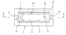
図1は本発明の一実施例の電子部品用パツケージ用Aの斜視図、図2は図1の電子部品用パツケージ用Aの平面図、図3は図2の電子部品用パツケージ用AののA−A線に沿う縦断面図である。
また、図4は本発明の電子部品組立構体の製造方法について説明するための製造工程ブロック図である。
まず、図1ないし図3に示す電子部品用パツケージ用Aを製作する(図4a)。図1ないし図3に示す電子部品用パツケージ用Aにおいて、1はベースの一例としての熱膨張係数が10〜15×10−6/℃のガラスセラミック製の絶縁性ベース(以下、単にベースという)で、底板部2と枠体部3とを有し、長手方向の両端部に電子素子用電極を形成するための凹部4、5を有する。このような熱膨張係数のベース1は、例えば、ガラス中に30〜70wt%のフォルステライト粉末を含むガラスセラミックで製作することができる。6、7は前記底板部2の上面からベース1の内方から外方に導出されている電子素子用電極で、一方の電極6は前記一方の凹部4の端面部を通って前記枠体部3の上面にまで延在してされており、他方の電極7は枠体部3の下を迂回して他方の凹部5の端面部を通って枠体部3の上面にまで延在してされている。8は前記電極6、7と同一材料でかつ同時に形成された、後述する水晶振動素子等の電子素子を支持するための、いわゆる「枕」と称せられる支持部である。9は前記枠体部3の上面に前記電子素子用電極6、7と離隔して形成された枠状の接地兼封止用電極である。2点鎖線で示す10は、水晶振動素子等の電子素子である。
前記電子部品用パツケージ用Aにおいては、ベース1の開口部を図11ないし図13に示すようなキャップ79で封止していないので、図11ないし図13に示す従来の気密パツケージに比較して、そのキャップ9の高さ寸法t2だけ小さくなり、それに応じて全体の高さ寸法t1は従来の高さ寸法t3に比較して小さくでき、低背化ができる。
【0014】
次に、上記の電子部品用パッケージAを用いて、その枠体部3の上面の電子素子用電極6、7および接地兼封止用電極9にはんだ等の導電性接着材11、12および導電性封止材13を被着形成する。さらに前記電子素子用電極6、7に水晶振動素子等の電子素子10を導電性接着材14、15で電気的に接続するとともに機械的に固着して、図5に示す電子部品中間構体Bを製作する(図4b)。ここで、前記導電性封止材11、12および導電性封止材13は、この電子部品中間構体Bを後述するプリント基板等の取付基板に固着する際の温度で溶融する融点を有するもので形成する。また、前記水晶振動素子等の電子素子10を接続固着する導電性接着材14、15は、前記導電性封止材11、12および導電性封止材13の融点よりも高い融点のものを用いる。
【0015】
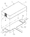
図6は前記電子部品中間構体Bと、この電子部品中間構体Bを組み付けるプリント基板等の取付基板50の組み付け前の斜視図である。図において、電子部品中間構体Bは、組み立てのために裏返しの状態になっており、取付基板50は、前記電子部品中間構体Bの電子素子用電極6、7を接続するための回路端子51、52と、この回路端子51、52から離隔した矩形状の接地電極53とを有する。
そして、前記電子部品中間構体Bの電子素子用電極6、7に被着された導電性接着材11、12をそれぞれ前記回路端子51、52に、また、前記接地兼封止用電極9に被着された導電性封止材13を前記接地電極53に重ね合わせ、加圧しながら加熱することにより、前記電子素子用電極6、7に被着された導電性接着材11、12を溶融させて電子素子用電極6、7をそれぞれ前記回路端子51、52に接続すると同時に、前記接地兼封止用電極9に被着された導電性封止材13を溶融させて接地兼封止用電極9を前記接地電極53に固着封止する(図4c)。このようにして、前記電子部品中間構体Bの開口部の封止と、電子部品中間構体Bの基板50への組み付けが同時に実施できる。
このため、電子素子10は、電子部品中間構体Bを取付基板50に組み付ける時に、一回だけ加熱されるだけであるから、加熱に伴う特性変動が生じ難くなるという特長がある。
図7は電子部品中間構体Bを基板50へ組み付けた状態の電子部品組立構体Cの縦断面図を示す。この電子部品組立構体Cにおいても、当然のことながら、キャップを用いていないので、全体の低背化が実現される。また、接地電極53によって、電子部品中間構体Bの接地兼封止電極9が接地されるので、浮遊容量や外来電磁波による電子素子10の特性変動が防止できる。
【0016】
なお、上記実施例は特定の構成の電子部品用パツケージAについて説明したが、本発明はこの構成の電子部品用パツケージAに限定されるものではなく、本発明の精神を逸脱しない範囲で各種の変形された構成が採用できる。
例えば、上記の電子部品用パツケージAでは、図に示す従来の絶縁性ベース1と同一寸法のベース1を用いてその枠体部3の上面に電子素子用電極6、7と、接地兼封止用電極9とを形成したものを示したが、図8に示す電子部品用パツケージDのように、絶縁性ベース21の長手方向の両端部の枠体部3の幅寸法w1を、短手方向の両端部の枠体部3の幅寸法w2よりも大きくしてもよい。そのようにすると、枠体部3の上面における電子素子用電極6、7と接地兼封止用電極9の面積を大きくできるので、取付基板50への組み付けが容易になるし、電子素子用電極6、7と接地兼封止用電極9とをさらに離隔して形成できるので、取付基板50への組み付け時に、高度の位置決めをしなくても、電子素子用電極6、7と接地兼封止用電極9とが短絡することを確実に防止できる特長がある。
【0017】
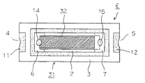
また、図9は電子素子用電極6、7を底板部2の長手方向の両端部に振り分けて形成した絶縁性ベース31を用いるとともに、水晶振動素子等の電子素子として両持ち用の電子素子32を用いたものでもよい。このようにすると、電極7を枠体部3の下を迂回して長手方向の他端部まで延在させる必要がなくなり、底板部2と枠体部3との密着性がよくなり、両者のデラミネーションが発生しなくなるのみならず、電極形成材料の使用量を節減できるし、電子素子32を安定して支持できる特長がある。
【0018】
さらに、上記実施例の電子部品用パツケージAおよびBは、ベース1、21または31の枠体部3の上面にのみ接地兼封止用電極9を形成する場合について説明したが、図10に示すように、ベース41の底板部2の全面に接地用導体層16を形成してもよい。なお、ベース41の長手方向の両端部に形成された凹部4、5の端面部には、図1に示す電子部品用パッケージAと異なり、上半分(図10の状態では下半分)のみに電子素子用電極6、7が形成されている。また、前記ベース41の短手方向の両端部には、凹部17、18を有し、これらの凹部17、18の端面部全面には、前記接地用導体層19が電気的に接続された接地用電極19、20が形成されている。
図中、60はプリント基板等の取付基板で、電子素子用電極6、7が接続される回路端子61、62と、ベース41の枠体部3の上面に形成された接地兼封止用電極9および前記ベース41の底板部2の下面に形成された接地用導体層16を接続固着するための接地電極63とを有する。ここで、前記接地電極63は、図6に示す接地電極51よりも大面積に形成されている。
このような構成によれば、前記ベース41の底板部2の下面の接地用導体層16が凹部17、18に形成された接地用電極19、20を介して接地されるので、浮遊容量や外来電磁波による電子素子10、32の特性変動をより確実に防止できるという特長がある。
【0019】
【発明の効果】
本発明は以上のように、底板部および枠体部とを有するベースと、このベースの内方からベースの外方に導出され前記枠体部の端面部を通って枠体部の上面部まで形成された電子素子用電極と、前記ベースの枠体部の上面部に前記電子素子用電極と離隔して形成された接地兼封止用電極とを有する電子部品用パッケージであるから、キャップを必要としない電子部品用パッージを提供できる。
本発明はまた、底板部および枠体部とを有するベースと、このベースの内方からベースの外方に導出され前記枠体部の端面部を通って枠体部の上面部まで形成された電子素子用電極と、前記ベースの枠体部の上面部に前記電子素子用電極と離隔して形成された接地兼封止用電極と、前記接地兼封止用電極に被着された導電性封止材とを有する電子部品用パツケージにおける前記電子素子用電極に電子素子を接続固着してなる電子部品中間構体を、前記ベースの開口部をキャップで封止することなく、前記電子素子用電極を取付基板の回路端子に接続するとともに、前記導電性封止材で取付基板に気密に固着封止した電子部品組立構体であるから、キャップを必要とせず、全体の低背化が実現できる。
本発明はさらに、底板部および枠体部とを有するベースと、このベースの内方からベースの外方に導出され前記枠体部の端面部を通って枠体部の上面部まで形成された電子素子用電極と、前記ベースの枠体部の上面部に前記電子素子用電極と離隔して形成された接地兼封止用電極と、前記接地兼封止用電極に被着された導電性封止材とを有する電子部品用パツケージを製造する工程と、前記電子部品用パツケージにおける電子素子用電極に電子素子を接続固着して電子部品中間構体を製作する工程と、前記ベースの開口部をキャップで封止することなく、前記電子素子用電極を取付基板の回路端子に接続すると同時に、前記導電性封止材で取付基板に気密に固着封止する工程とを有する電子部品組立構体の製造方法であるから、キャップを必要としない電子部品組立構体用が提供できるという効果を奏する。
【図面の簡単な説明】
【図1】本発明の一実施例の電子部品用パツケージ用Aの斜視図
【図2】図1の電子部品用パツケージ用Aの平面図
【図3】図2の電子部品用パツケージ用AのA−A線に沿う縦断面図
【図4】本発明の電子部品組立構体の製造方法を説明するための製造工程ブロック図
【図5】図1の電子部品用パツケージ用Aに電子素子を組み付けた電子部品中間構体Bの平面図
【図6】図5の電子部品中間構体Bを取付基板に組み付ける前の電子部品中間構体Bおよび取付基板の斜視図
【図7】図6の電子部品中間構体Bおよび取付基板の組み付け後の電子部品組立構体Cの縦断面図
【図8】本発明の第2実施例の電子部品用パッケージDの平面図
【図9】本発明の第3実施例の電子部品用パッケージを用いた電子部品中間構体Eの平面図
【図10】本発明の第4実施例の電子部品用パッケージを用いた電子部品中間構体Fおよび取付基板の組み付け前の斜視図
【図11】従来の気密パツケージを用いた電子部品の斜視図
【図12】図11の従来の気密パッケージを用いた電子部品のキャップおよび封止材の一部を除去した平面図
【図13】図12の従来の電子部品のB−B線に沿う縦断面図
【図14】従来の電子部品の製造方法を説明するための製造工程ブロック図
【符号の説明】
A、D 電子部品用パッケージ
B、E、F 電子部品中間構体
C 電子部品組立構体
1、21、31、41 ベース
2 底板部
3 枠体部
6、7 電子素子用電極
9 接地兼封止用電極
10、32 電子素子(水晶振動素子)
11、12、14、15 導電性接着材
13 導電性封止材
16 接地用導体層
19.20 接地用電極
60 取付基板(プリント基板)
52、61、62 回路端子
53、63 接地電極[0001]
TECHNICAL FIELD OF THE INVENTION
The present invention relates to a package for an electronic component that houses an electronic element such as a crystal oscillator, a crystal oscillator, and a SAW device.
The present invention also relates to an electronic component assembly structure in which an electronic component intermediate structure in which an electronic element is assembled in the electronic component package is mounted on a mounting board such as a printed circuit board.
The present invention further relates to a method for manufacturing the electronic component assembly.
[0002]
[Prior art]
As an airtight package for quartz oscillators, quartz oscillators and SAW devices, an insulating base, electrodes extending from the inside of the insulating base to the outside of the insulating base, and an opening in the insulating base are sealed. There is an airtight package having a cap hermetically sealed via a stopper. There are various types of such hermetic packages depending on the shape of the crystal vibrating element or the like. For example, as an airtight package for a rectangular plate-shaped quartz-crystal vibrating element, there is one disclosed in Japanese Utility Model Laid-Open No. 6-77328. Typical examples will be described below.
FIG. 11 is a perspective view of a conventional hermetic package, FIG. 12 is a plan view of the sealing material and a part of the cap removed, and FIG. 13 is a longitudinal sectional view taken along line BB of FIG.
11 to 13,
In the hermetic package having the above-described configuration, since an insulating cap such as alumina ceramic is used as the
Therefore, it has been considered to use a metal cap instead of the
Therefore, it is considered that an intermediate metal frame having an intermediate thermal expansion coefficient between the
[0003]
Accordingly, the present applicant has developed an insulating base made of glass ceramic having a thermal expansion coefficient of 10 to 15 × 10 −6 / ° C. in which 30 to 70 wt% of forsterite powder is mixed in glass, and this insulating base has been developed. An airtight package was proposed in which a metal cap made of stainless steel having a thermal expansion coefficient metal similar to this was sealed with a sealing material. According to the hermetic package having such a configuration, since the thermal expansion coefficients of the insulating base and the metal cap are close to each other, there is no stress due to the difference in the thermal expansion coefficient, and the hermetic package does not cause the characteristic fluctuation of the electronic element. Package can be provided. Further, if the metal cap is grounded, there is no fluctuation in the characteristics of the electronic element due to stray capacitance or external electromagnetic waves.
The method for manufacturing an electronic component using an airtight package in which the
[0004]
[Problems to be solved by the invention]
However, even in the hermetic package having the above structure, a metal cap is required, and there is a limit to the reduction in height of the hermetic package. Further, the metal cap is hermetically sealed to the frame portion of the insulating base via a sealing material. Therefore, it is necessary to seal the cap, assemble the electronic component to the mounting board, and perform two heating steps, and the characteristics of the
Therefore, an object of the present invention is to provide an electronic component package in which a cap can be omitted from the hermetic package.
Another object of the present invention is to provide an electronic component assembly using the electronic component package described above.
Still another object of the present invention is to provide a method for manufacturing an electronic component assembly using a package for electronic components.
[0005]
[Means for Solving the Problems]
The present invention provides a base having a bottom plate portion and a frame portion, and an electron drawn out from the inside of the base to the outside of the base and formed to an upper surface portion of the frame portion through an end surface portion of the frame portion. An electronic component package comprising: an element electrode; and a grounding / sealing electrode formed on an upper surface of the frame of the base so as to be separated from the electronic element electrode.
The present invention also provides a base having a bottom plate portion and a frame portion, and is formed to extend from the inside of the base to the outside of the base to the upper surface portion of the frame portion through the end surface of the frame portion. An electrode for an electronic element, an electrode for grounding and sealing formed on the upper surface of the frame portion of the base so as to be spaced apart from the electrode for the electronic element, and a seal adhered to the electrode for grounding and sealing. An electronic component intermediate structure in which an electronic element is connected and fixed to the electronic element electrode in the electronic component package having the material, the electronic element electrode is connected to a circuit terminal of a mounting board, and the sealing material is used. This is an electronic component assembly that is hermetically fixed and sealed to a mounting substrate.
The present invention further includes a base having a bottom plate portion and a frame portion, and is formed from the inside of the base to the outside of the base and formed through the end surface portion of the frame portion to the upper surface portion of the frame portion. An electrode for an electronic element, a grounding / sealing electrode formed on the upper surface of the frame portion of the base so as to be separated from the electrode for the electronic element, and a conductive material attached to the grounding / sealing electrode. A step of preparing an electronic component package having a sealing material; a step of connecting and fixing an electronic element to an electronic element electrode in the electronic component package to produce an electronic component intermediate structure; and Connecting to the circuit terminals of the mounting substrate and hermetically sealing and sealing the mounting substrate with the sealing material at the same time.
[0006]
BEST MODE FOR CARRYING OUT THE INVENTION
The invention according to
[0007]
According to a second aspect of the present invention, there is provided a base for a base having a bottom plate and a frame, and an electronic device formed to extend from the inside to the outside of the base to the end face and the top of the frame. An electrode comprising: an electrode; a grounding / sealing electrode formed on the upper surface of the frame body separately from the electronic element electrode; and a sealing material attached to the grounding / sealing electrode. It is a package for parts.
[0008]
According to a third aspect of the present invention, there is provided a base having a bottom plate portion and a frame portion, and an electronic device which is led out from the inside of the base to the outside and formed up to an end surface portion and an upper surface portion of the frame portion. An electrode, a grounding / sealing electrode formed on the upper surface of the frame body portion and spaced apart from the electronic element electrode, and a conductive sealing material applied to the grounding / sealing electrode. It is a package for electronic components having.
[0009]
According to a fourth aspect of the present invention, there is provided a base having a bottom plate portion and a frame portion, and an electronic device which is led out from the inside of the base to the outside and formed up to an end surface portion and an upper surface portion of the frame portion. An electrode, a grounding / sealing electrode formed in a frame shape on the upper surface of the frame body and separated from the electronic element electrode; and a conductive material formed of solder applied to the grounding / sealing electrode. It is an electronic component package having a conductive sealing material.
[0010]
The invention according to
[0011]
According to a sixth aspect of the present invention, there is provided a base for a base having a bottom plate portion and a frame portion, and an electronic device formed to extend from the inside to the outside of the base to the end surface portion and the top surface portion of the frame portion. An electrode; a grounding / sealing electrode formed in a frame shape on the upper surface of the frame body apart from the electronic element electrode; and a conductive sealing material applied to the grounding / sealing electrode. In the electronic component package having the electronic component electrode, the electronic component electrode is electrically connected to the circuit electrode of the mounting board without sealing the buttocks intermediate structure in which the electronic element is connected and fixed to the electronic element electrode. An electronic component assembly structure, wherein the electronic component assembly is connected and hermetically sealed and sealed to the ground electrode formed on the mounting substrate with the conductive sealing material.
[0012]
According to a seventh aspect of the present invention, there is provided a base having a bottom plate portion and a frame portion, and an electronic device formed to extend from the inside to the outside of the base to the end surface portion and the top surface portion of the frame portion. An electrode; a grounding / sealing electrode formed in a frame shape on the upper surface of the frame body apart from the electronic element electrode; and a conductive sealing material applied to the grounding / sealing electrode. Preparing an electronic device package having: an electronic component intermediate structure in which an electronic device is connected and fixed to the electronic device electrode; and electrically connecting the electronic device electrode to a circuit terminal of a mounting board. A method for manufacturing an electronic component assembly, characterized in that the grounding and sealing electrode is hermetically fixed and sealed to the ground electrode formed on the mounting substrate with the conductive sealing material at the same time as the connection is made.
[0013]
【Example】
Embodiments of the present invention will be described below with reference to the drawings.
FIG. 1 is a perspective view of an electronic component package A of one embodiment of the present invention, FIG. 2 is a plan view of the electronic component package A of FIG. 1, and FIG. 3 is a diagram of the electronic component package A of FIG. It is a longitudinal cross-sectional view which follows the AA line.
FIG. 4 is a manufacturing process block diagram for explaining a method for manufacturing an electronic component assembly according to the present invention.
First, an electronic component package A shown in FIGS. 1 to 3 is manufactured (FIG. 4a). In the package A for electronic components shown in FIGS. 1 to 3,
In the electronic component package A, since the opening of the
[0014]
Next, using the above electronic component package A, the
[0015]
FIG. 6 is a perspective view of the electronic component intermediate structure B and a mounting
Then, the
For this reason, since the
FIG. 7 is a longitudinal sectional view of an electronic component assembly structure C in a state where the electronic component intermediate structure B is mounted on the
[0016]
Although the above embodiment has been described with reference to the electronic component package A having a specific configuration, the present invention is not limited to the electronic component package A having this configuration, and various types of electronic component packages A may be used without departing from the spirit of the present invention. A modified configuration can be employed.
For example, in the above-mentioned electronic component package A, using the
[0017]
9 uses an insulating
[0018]
Further, in the electronic component packages A and B of the above embodiment, the case where the grounding / sealing electrode 9 is formed only on the upper surface of the frame portion 3 of the
In the figure,
According to such a configuration, the
[0019]
【The invention's effect】
As described above, the present invention provides a base having a bottom plate portion and a frame portion, and is drawn out from the inside of the base to the outside of the base, through the end surface portion of the frame portion to the upper surface portion of the frame portion. Since the electronic component package has the formed electronic element electrode and the grounding / sealing electrode formed on the upper surface of the frame portion of the base and separated from the electronic element electrode, the cap is provided. An unnecessary package for electronic components can be provided.
The present invention also provides a base having a bottom plate portion and a frame portion, and is formed to extend from the inside of the base to the outside of the base to the upper surface portion of the frame portion through the end surface of the frame portion. An electrode for an electronic element, a grounding / sealing electrode formed on the upper surface of the frame portion of the base so as to be separated from the electrode for the electronic element, and a conductive material attached to the grounding / sealing electrode. An electronic component intermediate structure in which an electronic device is connected and fixed to the electronic device electrode in the electronic component package having a sealing material, without sealing the opening of the base with a cap. Is connected to the circuit terminals of the mounting board, and the electronic component assembly is hermetically sealed to the mounting board with the conductive sealing material. Therefore, no cap is required and the overall height can be reduced.
The present invention further includes a base having a bottom plate portion and a frame portion, and is formed from the inside of the base to the outside of the base and formed through the end surface portion of the frame portion to the upper surface portion of the frame portion. An electrode for an electronic element, a grounding / sealing electrode formed on the upper surface of the frame portion of the base so as to be separated from the electrode for the electronic element, and a conductive material attached to the grounding / sealing electrode. Manufacturing a package for an electronic component having a sealing material, a process of connecting and fixing an electronic device to an electrode for an electronic device in the package for the electronic component to manufacture an electronic component intermediate structure, and an opening of the base. Connecting the electrode for electronic element to the circuit terminal of the mounting substrate without sealing with a cap, and simultaneously hermetically sealing and sealing the mounting substrate with the conductive sealing material. Method, so you need a cap An effect that can be provided for electronic assembly structure that does not.
[Brief description of the drawings]
1 is a perspective view of an electronic component package A according to an embodiment of the present invention; FIG. 2 is a plan view of the electronic component package A of FIG. 1; FIG. 3 is a plan view of the electronic component package A of FIG. FIG. 4 is a longitudinal sectional view taken along line AA. FIG. 4 is a block diagram of a manufacturing process for explaining a method of manufacturing an electronic component assembly according to the present invention. FIG. FIG. 6 is a plan view of the electronic component intermediate structure B shown in FIG. 6. FIG. 6 is a perspective view of the electronic component intermediate structure B and the mounting substrate before the electronic component intermediate structure B of FIG. FIG. 8B is a vertical cross-sectional view of the electronic component assembly structure C after mounting the mounting board. FIG. 8 is a plan view of an electronic component package D according to a second embodiment of the present invention. FIG. FIG. 10 is a plan view of an electronic component intermediate structure E using a component package. FIG. 11 is a perspective view of an electronic component intermediate structure F and a mounting board using a package for electronic components according to a fourth embodiment of the present invention before being assembled. FIG. 11 is a perspective view of an electronic component using a conventional hermetic package. FIG. 13 is a plan view of the conventional electronic component using the hermetic package of FIG. 13 with a cap and a part of a sealing material removed. FIG. 13 is a longitudinal sectional view of the conventional electronic component of FIG. Block diagram for explaining a method of manufacturing an electronic component of the present invention.
A, D Electronic component package B, E, F Electronic component intermediate structure C Electronic
11, 12, 14, 15 Conductive adhesive 13
52, 61, 62
Claims (7)
Priority Applications (1)
| Application Number | Priority Date | Filing Date | Title |
|---|---|---|---|
| JP36496898A JP3556111B2 (en) | 1998-12-22 | 1998-12-22 | Package for electronic component, electronic component assembly using the same, and method of manufacturing electronic component assembly |
Applications Claiming Priority (1)
| Application Number | Priority Date | Filing Date | Title |
|---|---|---|---|
| JP36496898A JP3556111B2 (en) | 1998-12-22 | 1998-12-22 | Package for electronic component, electronic component assembly using the same, and method of manufacturing electronic component assembly |
Publications (2)
| Publication Number | Publication Date |
|---|---|
| JP2000188459A JP2000188459A (en) | 2000-07-04 |
| JP3556111B2 true JP3556111B2 (en) | 2004-08-18 |
Family
ID=18483114
Family Applications (1)
| Application Number | Title | Priority Date | Filing Date |
|---|---|---|---|
| JP36496898A Expired - Fee Related JP3556111B2 (en) | 1998-12-22 | 1998-12-22 | Package for electronic component, electronic component assembly using the same, and method of manufacturing electronic component assembly |
Country Status (1)
| Country | Link |
|---|---|
| JP (1) | JP3556111B2 (en) |
-
1998
- 1998-12-22 JP JP36496898A patent/JP3556111B2/en not_active Expired - Fee Related
Also Published As
| Publication number | Publication date |
|---|---|
| JP2000188459A (en) | 2000-07-04 |
Similar Documents
| Publication | Publication Date | Title |
|---|---|---|
| US6456168B1 (en) | Temperature compensated crystal oscillator assembled on crystal base | |
| JP2008131549A (en) | Quartz oscillation device | |
| JP2002198739A (en) | Surface mount piezoelectric oscillator | |
| JP2009044753A (en) | Piezoelectric oscillator | |
| JP4730418B2 (en) | Piezoelectric oscillator | |
| JP3556111B2 (en) | Package for electronic component, electronic component assembly using the same, and method of manufacturing electronic component assembly | |
| JP4730419B2 (en) | Method for manufacturing piezoelectric oscillator | |
| JP2006033413A (en) | Piezoelectric vibration device | |
| JPH02105710A (en) | Crystal resonator | |
| JP2002084159A (en) | Surface-mounted piezoelectric vibrator | |
| JP2010166626A (en) | Piezoelectric device | |
| JPS6150413A (en) | Manufacture of piezoelectric vibrator | |
| JP2000269772A (en) | Electronic component | |
| JP2003133886A (en) | Crystal oscillator | |
| JP2000315918A (en) | Crystal oscillator | |
| JP3018977B2 (en) | Ceramic package, surface mount type piezoelectric vibrator, and method of forming electrodes of ceramic package | |
| JP2004297209A (en) | Surface mount piezoelectric vibrator | |
| JP2007124514A (en) | Piezoelectric oscillator and method of manufacturing the same | |
| JP3985489B2 (en) | Structure of piezoelectric vibrator | |
| JP2004064651A (en) | Surface-mounted piezoelectric oscillator | |
| JP2003110398A (en) | Piezoelectric device | |
| JP2001094380A (en) | Package for piezoelectric oscillation device | |
| JP2002261548A (en) | Piezoelectric device | |
| CN117063391A (en) | Constant temperature bath type piezoelectric oscillator | |
| JP2004297208A (en) | Surface mount type piezoelectric vibrator |
Legal Events
| Date | Code | Title | Description |
|---|---|---|---|
| TRDD | Decision of grant or rejection written | ||
| A01 | Written decision to grant a patent or to grant a registration (utility model) |
Free format text: JAPANESE INTERMEDIATE CODE: A01 Effective date: 20040511 |
|
| A61 | First payment of annual fees (during grant procedure) |
Free format text: JAPANESE INTERMEDIATE CODE: A61 Effective date: 20040511 |
|
| R150 | Certificate of patent or registration of utility model |
Free format text: JAPANESE INTERMEDIATE CODE: R150 |
|
| S531 | Written request for registration of change of domicile |
Free format text: JAPANESE INTERMEDIATE CODE: R313531 |
|
| R350 | Written notification of registration of transfer |
Free format text: JAPANESE INTERMEDIATE CODE: R350 |
|
| R250 | Receipt of annual fees |
Free format text: JAPANESE INTERMEDIATE CODE: R250 |
|
| FPAY | Renewal fee payment (event date is renewal date of database) |
Free format text: PAYMENT UNTIL: 20090521 Year of fee payment: 5 |
|
| LAPS | Cancellation because of no payment of annual fees |