JP3552600B2 - Substrate processing equipment - Google Patents
Substrate processing equipment Download PDFInfo
- Publication number
- JP3552600B2 JP3552600B2 JP19556899A JP19556899A JP3552600B2 JP 3552600 B2 JP3552600 B2 JP 3552600B2 JP 19556899 A JP19556899 A JP 19556899A JP 19556899 A JP19556899 A JP 19556899A JP 3552600 B2 JP3552600 B2 JP 3552600B2
- Authority
- JP
- Japan
- Prior art keywords
- unit
- substrate
- temperature
- holding
- coating
- Prior art date
- Legal status (The legal status is an assumption and is not a legal conclusion. Google has not performed a legal analysis and makes no representation as to the accuracy of the status listed.)
- Expired - Fee Related
Links
Images


Classifications
-
- G—PHYSICS
- G03—PHOTOGRAPHY; CINEMATOGRAPHY; ANALOGOUS TECHNIQUES USING WAVES OTHER THAN OPTICAL WAVES; ELECTROGRAPHY; HOLOGRAPHY
- G03F—PHOTOMECHANICAL PRODUCTION OF TEXTURED OR PATTERNED SURFACES, e.g. FOR PRINTING, FOR PROCESSING OF SEMICONDUCTOR DEVICES; MATERIALS THEREFOR; ORIGINALS THEREFOR; APPARATUS SPECIALLY ADAPTED THEREFOR
- G03F7/00—Photomechanical, e.g. photolithographic, production of textured or patterned surfaces, e.g. printing surfaces; Materials therefor, e.g. comprising photoresists; Apparatus specially adapted therefor
- G03F7/70—Microphotolithographic exposure; Apparatus therefor
- G03F7/708—Construction of apparatus, e.g. environment aspects, hygiene aspects or materials
- G03F7/70858—Environment aspects, e.g. pressure of beam-path gas, temperature
- G03F7/70866—Environment aspects, e.g. pressure of beam-path gas, temperature of mask or workpiece
- G03F7/70875—Temperature, e.g. temperature control of masks or workpieces via control of stage temperature
Landscapes
- Health & Medical Sciences (AREA)
- Life Sciences & Earth Sciences (AREA)
- Atmospheric Sciences (AREA)
- Toxicology (AREA)
- Engineering & Computer Science (AREA)
- Environmental & Geological Engineering (AREA)
- Epidemiology (AREA)
- Public Health (AREA)
- Physics & Mathematics (AREA)
- General Physics & Mathematics (AREA)
- Photosensitive Polymer And Photoresist Processing (AREA)
- Exposure And Positioning Against Photoresist Photosensitive Materials (AREA)
- Exposure Of Semiconductors, Excluding Electron Or Ion Beam Exposure (AREA)
Description
【0001】
【発明の属する技術分野】
本発明は、例えば半導体ウエハやLCD基板等にレジスト塗布処理、現像処理等を施す基板処理装置に関する。
【0002】
【従来の技術】
従来から、例えば、半導体デバイスの製造プロセスにおけるフォトリソグラフィー工程においては、半導体ウエハの表面にレジスト膜を形成するレジスト塗布処理と、レジスト塗布後の半導体ウエハに対して露光処理を行った後に当該半導体ウエハに対して現像を行う現像処理とが行われるが、従来からこれらレジスト塗布処理と現像処理は、例えば日本国特公平2−30194号公報によっても公知なように、対応する各種処理ユニットが1つのシステム内に装備された複合処理システム内で、露光プロセスを挟んで所定のシーケンスに従って行われている。
【0003】
ところで、半導体デバイスにおいては、近年その回路パターンが微細化され、高集積化が図られている。このため、例えば、ステッパ等の露光装置によって半導体ウエハに所定の回路パターンを露光する場合、微細な回路パターンを正確に転写するため、厳密な位置合わせが行われているとともに、僅かな温度差による熱膨張および熱収縮による位置ずれも防止する必要があるため、厳密な温度調整等が行われている。
【0004】
【発明が解決しようとする課題】
上述したとおり、半導体デバイス等の回路パターンの転写を行うフォトリソグラフィーの工程においては、露光装置において、半導体ウエハ等の厳密な温度調整が行われている。
【0005】
しかしながら、半導体デバイス等においては、さらに高集積化が図られており、その回路パターンは、微細化されつつある。このため、フォトリソグラフィーの工程においても、さらに厳密な温度制御および処理の高速化によるスループットの向上を図ることが当然要求される。
【0006】
本発明の目的は、従来に比べてさらに厳密な温度制御を行うことができ、正確な回路パターンの転写を行うことができるとともに、処理の高速化によるスループットの向上を図ることのできる基板処理装置を提供することにある。
【0007】
【課題を解決するための手段】
上述した目的を達成するため、本発明の第1の観点は、レジストが塗布された基板を温度調整しつつ露光する露光装置と、前記基板にレジストを塗布する塗布部と、露光後の基板を現像処理する現像部と、前記塗布部及び前記現像部と前記露光装置との間に配置され、前記基板処理装置と前記露光装置との間で基板を受け渡しするためのインターフェース部と、前記塗布部と前記現像部とインターフェース部との間で基板を搬送するための搬送手段と、前記インターフェース部内に配置され、前記基板が保持される保持部と、前記露光装置における温度調整に応じて、前記保持部に保持された基板を温度調整する温度調整手段とを具備する。
【0008】
本発明では、インターフェース部に、前記露光装置における温度調整に応じて、保持部に保持された基板を温度調整する温度調整手段が設けられているので、インターフェース部で、基板を露光装置において要求される温度により近い温度に温度調整した状態で基板を露光装置に受け渡すことができる。したがって、露光装置において基板をより正確に、短時間に温調することが可能となり、正確な回路パターンの転写を行うことができるとともに、処理の高速化によるスループットの向上を図ることができる。
【0009】
本発明の一の実施形態では、前記露光装置が、基板を露光する際の温度を検出し、検出結果に応じた信号を出力する温度検出部を有し、前記温度調整手段が、前記温度検出部から出力された信号に応じて前記保持部に保持された基板を温度調整することを特徴とする。
【0010】
本発明の一の実施形態では、当該基板処理装置が、前記露光装置において基板を露光する際の温度を検出し、検出結果に応じた信号を出力する温度検出部を有し、前記温度調整手段が、前記温度検出部から出力された信号に応じて前記保持部に保持された基板を温度調整することを特徴とする。
【0011】
本発明の一の実施形態では、前記温度検出部から出力された信号を前記温度調整手段による温度調整に適合するように補償する手段を有し、前記温度調整手段が、前記補償された信号に応じて前記保持部に保持された基板を温度調整することを特徴とする。
【0012】
本発明の一の実施形態では、前記保持部が、複数の前記基板を保持可能とされたバッファカセットを有することを特徴とする。
【0013】
本発明の一の実施形態では、前記バッファカセットが、複数の前記基板を夫々が略平行になるよう載置可能に構成され、前記温度調整手段が、前記バッファカセットに載置された前記基板の間に当該基板と略平行に温度調整した気体を流すことを特徴とする。
【0014】
本発明の一の実施形態では、前記保持部が、前記基板を前記露光装置との間で受け渡しする部位に配置され、前記基板を載置可能とされたステージを有することを特徴とする。
【0015】
本発明の一の実施形態では、前記温度調整手段が、前記ステージを温度調整する手段を有することを特徴とする。
【0016】
本発明の一の実施形態では、前記ステージは、前記露光される前の基板が載置される第1の載置部と露光された後の基板が載置される第2の載置部とを有することを特徴とする。
【0017】
本発明の一の実施形態では、前記第1載置部及び前記第2の載置部が、それぞれ、基板を多段に収容する収容部と、前記収容部を覆うとともに、前記インターフェース部から前記収容部に多段に収容された各基板に対してアクセス可能とする第1の開口部及び前記露光装置から前記収容部に多段に収容された各基板に対してアクセス可能とする第2の開口部が設けられたカバー部材とを具備することを特徴とする。
【0018】
本発明の一の実施形態では、前記第1の開口部に対して開閉可能に配置された第1の扉と、前記第1の扉を開閉する第1の開閉機構と、前記第2の開口部に対して開閉可能に配置された第2の扉と、前記第2の扉を開閉する第2の開閉機構とを具備することを特徴とする。
【0019】
本発明の一の実施形態では、前記カバー部材により覆われた空間を排気する排気手段を更に具備することを特徴とする。
【0020】
本発明の一の実施形態では、前記第1載置部及び前記第2の載置部が、それぞれ、基板を多段に収容する収容部と、前記収容部を覆うとともに、前記インターフェース部から前記収容部に多段に収容された少なくとも1枚の基板に対してアクセス可能とする第1の開口部及び前記露光装置から前記収容部に多段に収容された少なくとも1枚の基板に対してアクセス可能とする第2の開口部が設けられたカバー部材と、前記収容部を昇降する昇降機構とを具備することを特徴とする。
【0021】
本発明の第2の観点は、レジストが塗布された基板を温度調整しつつ露光する露光装置に接続される基板処理装置において、前記基板にレジストを塗布する塗布部と、露光後の基板を現像処理する現像部と、前記塗布部及び前記現像部と前記露光装置との間に配置され、前記基板処理装置と前記露光装置との間で基板を受け渡しするためのインターフェース部と、前記塗布部と前記現像部とインターフェース部との間で基板を搬送するための搬送手段と、前記インターフェース部内に配置され、前記露光される前の基板が保持される第1の保持部と、前記インターフェース部内に配置され、露光された後の基板が保持される第2の保持部と、前記第1及び第2の保持部に対して温度調整された気体を供給する気体供給部と、前記第1の保持部と前記気体供給部との間に介挿され、前記気体供給部から供給される気体を更に温度調整する温度調整部とを具備することを特徴とする。
【0022】
本発明では、露光される前の基板が保持される第1の保持部に対して気体供給部から供給される気体を更に温度調整して供給するようにしたので、インターフェース部で、基板を露光装置において要求される温度により近い温度に温度調整し、状態で基板を露光装置に受け渡すことができる。したがって、露光装置において基板をより正確に、短時間に温調することが可能となり、正確な回路パターンの転写を行うことができるとともに、処理の高速化によるスループットの向上を図ることができる。
【0023】
本発明は、露光装置も含めた基板処理装置として把握することも可能である。
従って、本発明の第3の観点は、レジストが塗布された基板を温度調整しつつ露光する露光装置と、前記基板にレジストを塗布する塗布部と、露光後の基板を現像処理する現像部と、前記塗布部及び前記現像部と前記露光装置との間に配置され、前記基板処理装置と前記露光装置との間で基板を受け渡しするためのインターフェース部と、前記塗布部と前記現像部とインターフェース部との間で基板を搬送するための搬送手段と、前記インターフェース部内に配置され、前記基板が保持される保持部と、前記露光装置における温度調整に応じて、前記保持部に保持された基板を温度調整する温度調整手段とを具備することを特徴とする。
【0024】
また、本発明の第4の観点は、レジストが塗布された基板を温度調整しつつ露光する露光装置と、前記基板にレジストを塗布する塗布部と、露光後の基板を現像処理する現像部と、前記塗布部及び前記現像部と前記露光装置との間に配置され、前記基板処理装置と前記露光装置との間で基板を受け渡しするためのインターフェース部と、前記塗布部と前記現像部とインターフェース部との間で基板を搬送するための搬送手段と、前記インターフェース部内に配置され、前記露光される前の基板が保持される第1の保持部と、前記インターフェース部内に配置され、露光された後の基板が保持される第2の保持部と、前記第1及び第2の保持部に対して温度調整された気体を供給する気体供給部と、前記第1の保持部と前記気体供給部との間に介挿され、前記気体供給部から供給される気体を更に温度調整する温度調整部とを具備することを特徴とする。
【0025】
【発明の実施の形態】
以下、本発明の実施の形態を図面に基づき説明する。
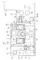
図1乃至図3は、本発明の基板処理装置の実施形態にかかるウエハの塗布現像処理システムの概略構成を示しており、図1はその平面図、図2はその正面図、図3はその背面図である。
【0026】
図1に示すように、この塗布現像処理システム100では、被処理体としてのウエハWをウエハカセットCRで複数枚、例えば25枚単位で外部からシステムに搬入・搬出したり、ウエハカセットCRに対してウエハWを搬入・搬出したりするためのカセットステーション10と、塗布現像工程の中で1枚ずつウエハWに所定の処理を施す枚葉式の各種処理ユニットを所定位置に多段配置した処理ステーション11と、塗布現像処理システム100に隣接して配設された露光装置200との間でウエハWを受け渡しするためのインターフェース部12とが一体的に接続されている。上記カセットステーション10では、カセット載置台20上の位置決め突起20aの位置に、複数個例えば4個までのウエハカセットCRが、各々ウエハ出入り口を処理ステーション11側に向けてX方向に一列に載置され、このカセット配列方向(X方向)及びウエハカセットCR内に収納されたウエハWのウエハ配列方向(Z方向:垂直方向)に移動可能なウエハ搬送体21が各ウエハカセットCRに選択的にアクセスする。
【0027】
このウエハ搬送体21はθ方向に回転自在であり、後述するように処理ステーション11側の第3の処理ユニット群G3の多段ユニット部に配設されたアライメントユニット(ALIM)やイクステンションユニット(EXT)にもアクセスできる。
【0028】
処理ステーション11には、ウエハ搬送装置を備えた垂直搬送型の主ウエハ搬送機構22が設けられ、その周りに全ての処理ユニットが1組または複数の組に亙って多段に配置されている。
【0029】
なお、この塗布現像処理システム100の近傍には、この塗布現像処理システム100との間で薬液の供給や廃液の処理・収容などを行う図示しないケミカルキャビネットが配設される。
【0030】
図2に示すように、第1の処理ユニット群Glでは、カップCP内でウエハWをスピンチャックに載せて所定の処理を行う2台のスピンナ型処理ユニット、例えばレジスト塗布ユニット(COT)および現像ユニット(DEV)が下から順に2段に重ねられている。第2の処理ユニット群G2では、2台のスピンナ型処理ユニット、例えばレジスト塗布ユニット(COT)および現像ユニット(DEV)が下から順に2段に重ねられている。これらレジスト塗布ユニット(COT)は、レジスト液の排液が機構的にもメンテナンスの上でも面倒であることから、このように下段に配置するのが好ましい。しかし、必要に応じて適宜上段に配置することももちろん可能である。
【0031】
図3に示すように、主ウエハ搬送機構22では、筒状支持体49の内側に、ウエハ搬送装置46が上下方向(Z方向)に昇降自在に装備されている。筒状支持体49はモータ(図示せず)の回転軸に接続されており、このモータの回転駆動力によって、前記回転軸を中心としてウエハ搬送装置46と一体に回転し、それによりこのウエハ搬送装置46はθ方向に回転自在となっている。なお筒状支持体49は前記モータによって回転される別の回転軸(図示せず)に接続するように構成してもよい。
【0032】
ウエハ搬送装置46には、搬送基台47の前後方向に移動自在な複数本の保持部材48が配設されており、これらの保持部材48は各処理ユニット間でのウエハWの受け渡しを可能にしている。
【0033】
また、図1に示すようにこの塗布現像処理システム100では、5つの処理ユニット群G1、G2、G3、G4、G5が配置可能であり、第1および第2の処理ユニット群Gl、G2の多段ユニットは、システム正面側に配置され、第3の処理ユニット群G3の多段ユニットはカセットステーション10に隣接して配置され、第4の処理ユニット群G4の多段ユニットはインターフェース部12に隣接して配置され、第5の処理ユニット群G5の多段ユニットは背面側に配置されることが可能である。
【0034】
図3に示すように、第3の処理ユニット群G3では、ウエハWを保持台(図1に示すSP)に載せて所定の処理を行うオープン型の処理ユニット、例えば冷却処理を行うクーリングユニット(COL)、レジストの定着性を高めるためのいわゆる疏水化処理を行うアドヒージョンユニット(AD)、位置合わせを行うアライメントユニット(ALIM)、イクステンションユニット(EXT)、露光処理前の加熱処理を行うプリベーキングユニット(PREBAKE)および露光処理後の加熱処理を行うポストベーキングユニット(POBAKE)が、下から順に例えば8段に重ねられている。第4の処理ユニット群G4でも、オープン型の処理ユニット、例えばクーリングユニット(COL)、イクステンション・クーリングユニット(EXTCOL)、イクステンションユニット(EXT)、クーリングユニット(COL)、プリベーキングユニット(PREBAKE)およびポストベーキングユニット(POBAKE)が下から順に、例えば8段に重ねられている。
【0035】
このように処理温度の低いクーリングユニット(COL)、イクステンション・クーリングユニット(EXTCOL)を下段に配置し、処理温度の高いプリベーキングユニット(PREBAKE)、ポストベーキングユニット(POBAKE)およぴアドヒージョンユニット(AD)を上段に配置することで、ユニット間の熱的な相互干渉を少なくすることができる。もちろん、ランダムな多段配置としてもよい。
【0036】
図1に示すように、インターフェース部12では、奥行方向(X方向)は前記処理ステーション11と同じ寸法を有するが、幅方向(Y方向)はより小さなサイズである。
【0037】
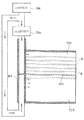
上記インターフェース部12の正面部には、図2に示すように、可搬性のピックアップ型のウエハカセットCRと、定置型のバッファカセットBRとが2段に配置されている。これらのカセットのうち、バッファカセットBRには、図4に示すように、ウエハWの温度調整を行う温度調整手段が設けられている。
【0038】
すなわち、図4に示す例では、バッファカセットBR内に温度調整された空気を導入するためのダクト60が設けられており、バッファカセットBRの背面側に設けられた空気流路61から、多数の透孔62を介して正面側(ウエハWの出入り口側)に向けて温度調整された空気を流し、バッファカセットBR内に配置されたウエハWの温度調整を行うよう構成されている。
【0039】
このウエハWの温度調整手段は、図5に示すように、空気の加熱および冷却を行う加熱器、冷却器、温度検出器等からなるBR温調用空気温度調整機構101と、このBR温調用空気温度調整機構101を制御するBR温調制御装置102等から構成されている。
【0040】
また、図5に示すように、露光装置200には、ウエハWの温調を行うための機構として、例えば、ウエハWを載置可能とされた温調プレート201が設けられており、この温調プレート201は、加熱器、冷却器等によって温調を行う温調部202aと温度検出器等からなる温度検出部202bとを有する露光装置基板温度調整機構202、この露光装置基板温度調整機構202を制御する露光装置温度制御装置203等を具備している。
【0041】
そして、前述したBR温調制御装置102は、露光装置基板温度調整機構202の温度検出部202bの温度検出信号又は、露光装置温度制御装置203から露光装置基板温度調整機構202に発せられる制御信号を入力し、その信号の傾向により、BR温調用空気温度調整機構101に対する制御信号を調整するよう構成されている。
【0042】
すなわち、通常、BR温調制御装置102において設定されるウエハWの制御目標温度は、露光装置温度制御装置203における制御目標温度と同一の温度に設定される。
【0043】
しかしながら、例えば温度制御特性の相違や、バッファカセットBRにおける温調の後のウエハW搬送工程の影響等により、バッファカセットBRにおける温調の後、露光装置200の温調プレート201において、例えば更にウエハWを主として、加熱方向に制御するようになる場合と、冷却方向に制御するようになる場合とが生じる。
【0044】
このため、例えば、露光装置200の温調プレート201において、ウエハWを主として、加熱方向に制御するようになる場合は、バッファカセットBRにおける温調の温度設定を、若干上昇させ、一方、露光装置200の温調プレート201において、ウエハWを主として、冷却方向に制御するようになる場合は、バッファカセットBRにおける温調の温度設定を、若干下降させるように、BR温調制御装置102において、BR温調用空気温度調整機構101に対する制御信号を調整する。なお、このような調整は後述する補償回路によって行うことも可能である(図12参照)。
【0045】
以上のようなバッファカセットBRにおけるウエハWの温調を行うことにより、露光装置200の温調プレート201におけるウエハWの温調を、より短時間に、かつ、正確に行うことができる。
【0046】
また、図1に示すように、インターフェース部12の背面部には周辺露光装置23が配設されている。
【0047】
図1に示すように、インターフェース部12の中央部には、基板搬送装置24が配設されている。この基板搬送装置24は、X方向、Z方向に移動して両カセットCR、BRおよび周辺露光装置23にアクセスする。
【0048】
また、基板搬送装置24は、θ方向にも回転自在であり、処理ステーション11側の第4の処理ユニット群G4の多段ユニットに配設されたイクステンションユニット(EXT)や、隣接する露光装置200側のウエハ受渡し台(図示せず)にもアクセスできる。
【0049】
ここで、基板搬送装置24として、処理ステーション11に設けられた主ウエハ搬送機構22と同様な搬送機構を設け、第4の処理ユニット群G4の多段ユニットに、インターフェース部12側からアクセスできるようにすれば、主ウエハ搬送機構22の負担を軽減することができ、ウエハWの搬送能力の向上による処理の迅速化を図ることもできる。
【0050】
また塗布現像処理システム100では、既述の如く主ウエハ搬送機構22の背面側にも図5中破線で示した第5の処理ユニット群G5の多段ユニットを配置できるが、この第5の処理ユニット群G5の多段ユニットは、案内レール25に沿ってY方向へ移動可能である。従って、この第5の処理ユニット群G5の多段ユニットを図示の如く設けた場合でも、前記案内レール25に沿って移動することにより、空間部が確保されるので、主ウエハ搬送機構22に対して背後からメンテナンス作業が容易に行える。
【0051】
次に、この塗布現像処理システム100によるウエハWの処理の流れについて説明する。
【0052】
まずカセットステーション10において、ウエハ搬送体21がカセット載置台20上の処理前のウエハWを収容しているカセットCRにアクセスして、そのカセットCRから1枚のウエハWを取り出す。その後、ウエハ搬送体21は、第3の処理ユニット群G3のアライメントユニット(ALIM)等を介して処理ステーション11側の主ウエハ搬送機構22にウエハWを受け渡す。
【0053】
主ウエハ搬送機構22は、上記アライメントユニット(ALIM)にてオリフラ合わせ及びセンタリングが完了したウエハWを取り出し、第3の処理ユニット群G3のアドヒージョンユニット(AD)にウエハWを搬入して疎水化処理を行う。
【0054】
疎水化処理を終えたウエハWは、その後主ウエハ搬送機構22によって所定のプリベーキングユニット(PREBAKE)に搬入されてベーキングされた後、所定のクーリングユニット(COL)に搬入される。このクーリングユニット(COL)内でウエハWはレジスト塗布処理前の設定温度例えば23℃まで冷却される。
【0055】
冷却処理が終了すると、ウエハWは主ウエハ搬送機構22によって所定のレジスト塗布ユニット(COT)へ搬入され、このレジスト塗布ユニット(COT)内でウエハW表面へのレジスト塗布が行われる。
【0056】
レジスト塗布処理が終了すると、主ウエハ搬送機構22はウエハWをレジスト塗布ユニット(COT)から取り出し、再び所定のプリベーキングユニット(PREBAKE)内へ搬入する。ウエハWはここで所定温度例えば100℃で所定時間加熱され、これによりウエハW上の塗布膜から残存溶剤が蒸発除去される。
【0057】
この後、ウエハWは主ウエハ搬送機構22によってイクステンション・クーリングユニット(EXTCOL)へ搬入される。ここで、ウエハWは、次工程つまり周辺露光装置23による周辺露光処理に適した温度例えば24℃まで冷却される。
【0058】
この後、インターフェース部12に設けられた前述した基板搬送装置24がイクステンション・クーリングユニット(EXTCOL)からウエハWを取り出すことによって、ウエハWが基板搬送装置24に受け渡される。
【0059】
次に、基板搬送装置24は当該ウエハWをインターフェース部12内の周辺露光装置23へ搬入する。ここで、ウエハWはその周縁部に露光処理を受ける。
【0060】
周辺露光処理が終了すると、基板搬送装置24は、ウエハWを周辺露光装置23から搬出し、隣接する露光装置200側のウエハ受取り台(図示せず)へ移送する。この場合、ウエハWは、露光装置200へ渡される前に、必要に応じてバッファカセットBRに一時的に格納される。
【0061】
そして、バッファカセットBRに一時的に格納されたウエハWは、前述したとおり、露光装置200における温調の状態を参照して、温調される。
【0062】
したがって、高精度なウエハWの温調を必要とする露光装置200側において、ウエハWの温調をより短時間に、正確に行うことが可能となる。
【0063】
上述したように、ウエハWが露光装置200に受け渡された後、露光装置200により、レティクルを用いた露光が行われる。露光装置200でのウエハW全面への露光処理が完了すると、ウエハWは、再度インターフェース部12の基板搬送装置24に受け渡される。
【0064】
そして、ウエハWは、さらに基板搬送装置24から処理ステーション11側へ受け渡される。なおこの場合、ウエハWを、処理ステーション11側へ渡される前に、必要に応じてインターフェース部12内のバッファカセットBRに一時的に格納するようにしてもよい。
【0065】
この後、処理ステーション11の主ウエハ搬送機構22は、受け取ったウエハWを所定のポストベーキングユニット(POBAKE)に搬入する。このポストベーキングユニット(POBAKE)において、ウエハWは熱板上に載置されて所定時間ベーク処理される。
【0066】
この後、ベーキングされたウエハWは主ウエハ搬送機構22によっていずれかのクーリングユニット(COL)に搬入され、このクーリングユニット(COL)内でウエハWは常温に戻される。続いて、ウエハWは主ウエハ搬送機構22によって所定の現像ユニット(DEV)に搬入される。
【0067】
この現像ユニット(DEV)内では、ウエハWはスピンチャックの上に載せられ、例えばスプレー方式により、ウエハW表面のレジストに現像液が均一にかけられて現像が行われる。そして現像後、ウエハW表面にリンス液がかけられ、現像液の洗い落しが行われ、この後ウエハWが高速回転されて乾燥が行われる。
【0068】
この後、主ウエハ搬送機構22は、ウエハWを現像ユニット(DEV)から搬出して、次に所定のポストベーキングユニット(POBAKE)ヘウエハWを再び搬入する。このポストベーキングユニット(POBAKE)において、ウエハWは例えば100℃で所定時間だけ加熱され、これによって、現像で膨潤したレジストが硬化し、耐薬品性が向上する。
【0069】
ポストベーキングが終了すると、主ウエハ搬送機構22はウエハWをポストベーキングユニットから搬出し、次に所定のクーリングユニット(COL)ヘウエハWを搬入して冷却処理が行われる。
【0070】
ウエハWが常温に戻った後、主ウエハ搬送機構22は、ウエハWをカセットステーション10側に受け渡し、カセットステーション10側のウエハ搬送体21は、受け取ったウエハWをカセット載置台20上の処理済みウエハ収容用のカセットCRの所定のウエハ収容溝に入れる。
【0071】
図6は、他の実施形態の構成を示すもので、この実施形態では、インターフェース部12内に、露光装置200との間でウエハWの受け渡しを行うための受け渡しステージとして、入口側受け渡しステージ28、出口側受け渡しステージ29が設けられている。
【0072】
そして、基板搬送装置24によって、ウエハWを入口側受け渡しステージ28に載置し、図示しない露光装置200側の搬送機構により、この入口側受け渡しステージ28上のウエハWを受け取ることによって、ウエハWを露光装置200に受け渡し、逆の手順で、出口側受け渡しステージ29を介して露光装置200から塗布現像処理システム100へウエハWを受け渡す構成となっている。
【0073】
また、ウエハWを露光装置200側に受け渡すための入口側受け渡しステージ28には、ウエハWを温調するための温度調整手段が設けられている。この温度調整手段は、図7に示すように、入口側受け渡しステージ28の加熱および冷却を行う加熱器、冷却器、温度検出器等からなるステージ温度調整機構111と、このステージ温度調整機構111を制御するステージ温調制御装置112等から構成されている。
【0074】
そして、ステージ温調制御装置112は、前述したBR温調制御装置102と同様に、露光装置基板温度調整機構202の温度検出部202bの温度検出信号又は、露光装置温度制御装置203から露光装置基板温度調整機構202に発せられる制御信号を入力し、その信号の傾向により、ステージ温度調整機構111に対する制御信号を調整するよう構成されている。
【0075】
すなわち、前述したとおり、例えば、露光装置200の温調プレート201において、ウエハWを主として、加熱方向に制御するようになる場合は、温度設定を、若干上昇させ、一方、露光装置200の温調プレート201において、ウエハWを主として、冷却方向に制御するようになる場合は、温度設定を、若干下降させるように、ステージ温調制御装置112において、ステージ温度調整機構111に対する制御信号を調整する。
【0076】
以上のような入口側受け渡しステージ28におけるウエハWの温調を行うことにより、露光装置200にウエハWを受け渡しする部位において、露光装置200にウエハWを受け渡しする直前までウエハWの温調を行うことができ、さらに、前述したとおり、露光装置200におけるウエハWの温調の状態を参照して温調を行っているため、露光装置200の温調プレート201におけるウエハWの温調を、より短時間に、かつ、正確に行うことができる。
【0077】
なお、この場合、前述した実施形態におけるバッファカセットBRにおける温調と伴用し、バッファカセットBRにおけるウエハWの温調と入口側受け渡しステージ28におけるウエハWの温調の双方を行うようにして、さらに効率よく、正確な温調を行えるようにすることもできる。
【0078】
また、この実施形態においては、図6に示すように、インターフェース部12内に、周辺露光装置を配置しない構成となっており、このため、インターフェース部12のX方向の長さが前述した図1の構成の場合に比べて短くなっている。このため、露光装置200に対するメンテナンス等の際のアクセスを容易に行える。
【0079】
特に、露光装置200においては、露光ステージに対するメンテナンス等を頻繁に行う必要があり、このため、従来においては、塗布現像処理システム100のインターフェース部12を前方に引き出す等して、露光装置200の塗布現像処理システム100側から、その内部の露光ステージにアクセスする等の必要があったが、図6に示す構成の場合、インターフェース部12のX方向の長さが短くなっているので、インターフェース部12を引き出すことなく、背面側から露光装置200の側面(塗布現像処理システム100側)に対して容易にアクセスすることができる。
【0080】
上記構成の場合、周辺露光装置は、前述した処理ステーション11の中の処理ユニット群のいずれかの部位に配置する。
【0081】
以上のとおり、上述した各実施形態によれば、バッファカセットBR、または露光装置200にウエハWを受け渡しする部位である入口側受け渡しステージ28、あるいはこれら双方において、露光装置200におけるウエハWの温調の状態を参照して温調を行っているため、露光装置200の温調プレート201におけるウエハWの温調を、より短時間に、かつ、正確に行うことができる。
【0082】
したがって正確な回路パターンの転写を行うことができるとともに、処理の高速化によるスループットの向上を図ることができる。
【0083】
次に本発明の別の実施形態を説明する。
【0084】
図6に示した実施形態では、インターフェース部12内に、入口側受け渡しステージ28、出口側受け渡しステージ29を設けていたが、本実施形態では、図8及び図9に示すように示すように、これらのステージをそれぞれ多段に構成した入口側受け渡し収容部401、出口側受け渡し収容部402としている。入口側受け渡し収容部401には、露光装置200へ受け渡されるウエハWが収容される。出口側受け渡し収容部402には、露光装置200から受け渡されたウエハWが収容される。
【0085】
入口側受け渡し収容部401及び出口側受け渡し収容部402はカバー403により覆われている。また、カバー403のインターフェース部12側には、基板搬送装置24が入口側受け渡し収容部401及び出口側受け渡し収容部402に収容されたウエハWに対してアクセスができるように開口部404、405がそれぞれ設けられている。また、カバー403の露光装置200側には、露光装置200の搬送アーム367が入口側受け渡し収容部401及び出口側受け渡し収容部402に収容されたウエハWに対してアクセスができるように開口部406、407がそれぞれ設けられている。各開口部404〜407には、駆動機構408により開閉される扉409が設けられている。この扉409は、ウエハWが入口側受け渡し収容部401または出口側受け渡し収容部402に搬入出される際に開き、それ以外の時には閉じている。
【0086】
またカバー403内は仕切板412により2つの第1及び第2の室413、414に区切られており、第1の室413には入口側受け渡し収容部401が配置され、第2の室414には出口側受け渡し収容部402が配置されている。
【0087】
図8において符号710は第1及び第2の室413、414に温度調整された清浄気体を供給する気体供給部である。そして、本実施形態では、気体供給部710から供給された清浄気体は出口側受け渡し収容部402が配置された第2の室414の上部より第2の室414に直接供給されるが、第1の室413に対しては入口側受け渡し収容部401が配置された第1の室413の上部より温度調整装置611を介して供給されるようになっている。
【0088】
また第1の室413の下部には排気口415が設けられ、第2の室414の下部には排気口416が設けられている。排気口415、416には排気装置417が接続され、排気装置417によって第1及び第2の室413,414内が排気されるようになっている。
【0089】
本実施形態では、図6に示したインターフェース部12内の入口側受け渡しステージ28、出口側受け渡しステージ29に代えてこれらのステージをそれぞれ多段に構成した入口側受け渡し収容部401、出口側受け渡し収容部402としたことで、インターフェース部12内にバッファカセットBRを設けることを不要としている。これにより、装置の小型化を図ることができ、また作業員による装置内部へのアクセスが容易となり、メンテナンス等が容易となる。
【0090】
また、カバー403の各開口部404〜407に扉409を設け、ウエハWが入口側受け渡し収容部401または出口側受け渡し収容部402に搬入出される際以外の時には扉409を閉じるようにすることで、露光装置200側にパーティクルが流出することを防止できる。
【0091】
更に、現像処理ユニット(DEV)に比べて露光装置200の温度調整がより精密さが要求される。そこで、本実施形態では、上記のように露光前のウエハWが収容される第1の室413へは温度調整装置611によってより正確に温度調整された清浄気体を供給することによって、露光装置200における露光処理をより精密にかつ短時間で行うことが可能となる。
【0092】
図10は図8及び図9に示した実施形態の変形例の説明図である。
図10に示す実施形態では、カバー503の各開口部504〜507を少なくともウエハWを1枚出し入れできる大きさにすると共に、入口側受け渡し収容部501及び出口側受け渡し収容部502を昇降する昇降機構520、521を例えば入口側受け渡し収容部501及び出口側受け渡し収容部502の下部にそれぞれ設けている。そして、昇降機構520、521の昇降動作によって、入口側受け渡し収容部501及び出口側受け渡し収容部502おける受け渡しが必要な部位を開口部504〜507に合わせるようにしている。
【0093】
本実施形態では、開口部504〜507が非常に小さくなるので、露光装置200側にパーティクルが流出することを更に強力に防止できる。
【0094】
次に更に別の実施形態を説明する。
図11はこの実施形態に係るバッファカセットBRの説明図である。
【0095】
図11に示すように、このバッファカセットBRはその内部が仕切り板701によって上段室702と下段室703とに区切られている。上段室702には、露光装置200へ受け渡されるウエハWが収容される。下段室703には、露光装置200から受け渡されたウエハWが収容される。
【0096】
符号704は上段室702及び下段室703に温度調整された清浄気体を供給する気体供給部である。そして、本実施形態では、気体供給部704から供給された清浄気体は露光装置200から受け渡されたウエハWが収容される下段室703に直接供給されるが、露光装置200へ受け渡されるウエハWが収容される上段室702に対しては温度調整装置705を介して供給されるようになっている。
【0097】
本実施形態においても、露光装置200における露光処理をより精密にかつ短時間で行うことが可能となる。
【0098】
なお、図5に示した実施形態では、露光装置200側の検出信号を直接塗布現像処理システム100側に送っていたが、図12に示すように露光装置200側の検出信号を補償する補償回路901を介して塗布現像処理システム100側へ送るようにしてもよい。この補償回路901は露光装置200側の検出信号を塗布現像処理システム100側での温度調整に適合するように補償するものである。
【0099】
このように補償回路を設けることによって例えば従来構成の露光装置であっても塗布現像処理システム100側において本発明に係る技術を実現することが可能となる。
【0100】
また露光装置200側から検出信号が出力されないような場合には、例えば図13に示すように塗布現像処理システム100の露光装置200側に、露光装置200に向けて突出する温度検出機構910を設けてもよい。例えば温度検出機構910の先端には温度検出部が設けられており、塗布現像処理システム100と露光装置200とが接続されると、温度検出機構910が露光装置200内の温度を測定することが可能となっている。そして、温度検出機構910により検出された結果に基づきカセットバッファやステージの温度制御を行う。
【0101】
本発明は基板としてはウエハに限らず、フォトリソグラフィ技術が適用される基板であれば如何なる基板でもよく、例えば液晶ディスプレイ用のガラス基板であってもよい。
【0102】
【発明の効果】
以上説明したように、本発明によれば、露光装置において基板をより正確に、短時間に温調することが可能となり、正確な回路パターンの転写を行うことができるとともに、処理の高速化によるスループットの向上を図ることができる。
【図面の簡単な説明】
【図1】本発明の一実施形態に係る塗布現像処理システムの平面図である。
【図2】図1に示した塗布現像処理システムの正面図である。
【図3】図1に示した塗布現像処理システムの背面図である。
【図4】図1に示したバッファカセットの断面図である。
【図5】本発明の一実施形態に係る温度調整手段の説明図である。
【図6】本発明の他の実施形態に係る塗布現像処理システムの平面図である。
【図7】本発明の他の実施形態に係る温度調整手段の説明図である。
【図8】本発明のまた別の実施形態に係るステージの側面図である。
【図9】図8に示したステージの正面図である。
【図10】図8及び図9に示した実施形態の変形例に係るステージの側面図である。
【図11】本発明の更に別の実施形態に係るバッファカセットの説明図である。
【図12】図5に示した実施形態の変形例の説明図である。
【図13】更に別の変形例の説明図である。
【符号の説明】
W 半導体ウエハ(基板)
BR バッファカセット
100 塗布現像システム
200 露光装置
11 処理ステーション
12 インターフェース部[0001]
TECHNICAL FIELD OF THE INVENTION
The present invention relates to a substrate processing apparatus that performs, for example, a resist coating process, a developing process, and the like on a semiconductor wafer, an LCD substrate, and the like.
[0002]
[Prior art]
Conventionally, for example, in a photolithography step in a semiconductor device manufacturing process, a resist coating process for forming a resist film on the surface of a semiconductor wafer, and an exposure process for the semiconductor wafer after the resist coating are performed, and then the semiconductor wafer The resist coating process and the developing process are conventionally performed by a corresponding one of various processing units as well known in, for example, Japanese Patent Publication No. 2-30194. The processing is performed according to a predetermined sequence with the exposure process interposed in the complex processing system provided in the system.
[0003]
By the way, in semiconductor devices, circuit patterns thereof have recently been miniaturized, and high integration has been achieved. Therefore, for example, when a predetermined circuit pattern is exposed on a semiconductor wafer by an exposure apparatus such as a stepper, strict alignment is performed to accurately transfer a fine circuit pattern, and a slight temperature difference is applied. Since it is necessary to prevent displacement due to thermal expansion and thermal contraction, strict temperature adjustment and the like are performed.
[0004]
[Problems to be solved by the invention]
As described above, in the step of photolithography for transferring a circuit pattern of a semiconductor device or the like, strict temperature adjustment of a semiconductor wafer or the like is performed in an exposure apparatus.
[0005]
However, in semiconductor devices and the like, higher integration is being achieved, and circuit patterns thereof are being miniaturized. Therefore, in the photolithography process, it is naturally required to improve the throughput by stricter temperature control and higher processing speed.
[0006]
An object of the present invention is to provide a substrate processing apparatus capable of performing more strict temperature control as compared with the related art, performing accurate transfer of a circuit pattern, and improving throughput by increasing processing speed. Is to provide.
[0007]
[Means for Solving the Problems]
In order to achieve the above-described object, a first aspect of the present invention is directed to an exposure apparatus that performs exposure while adjusting the temperature of a substrate on which a resist is applied, an application unit that applies a resist to the substrate, and an exposed substrate. A developing unit for developing processing, an interface unit disposed between the coating unit and the developing unit and the exposure device, for transferring a substrate between the substrate processing device and the exposure device, and the coating unit Transport means for transporting a substrate between the developing unit and the interface unit; a holding unit arranged in the interface unit for holding the substrate; and a holding unit for adjusting the temperature in the exposure apparatus. Temperature adjusting means for adjusting the temperature of the substrate held by the unit.
[0008]
In the present invention, since the interface section is provided with a temperature adjusting means for adjusting the temperature of the substrate held by the holding section in accordance with the temperature adjustment in the exposure apparatus, the interface section is required to adjust the substrate in the exposure apparatus. The substrate can be delivered to the exposure apparatus in a state where the temperature is adjusted to a temperature closer to the temperature. Therefore, the temperature of the substrate can be more accurately controlled in a short time in the exposure apparatus, and the transfer of the circuit pattern can be performed accurately, and the throughput can be improved by increasing the processing speed.
[0009]
In one embodiment of the present invention, the exposure apparatus has a temperature detection unit that detects a temperature at the time of exposing the substrate and outputs a signal according to a detection result, and the temperature adjustment unit is configured to perform the temperature detection. The temperature of the substrate held by the holding unit is adjusted according to a signal output from the unit.
[0010]
In one embodiment of the present invention, the substrate processing apparatus has a temperature detection unit that detects a temperature at which the exposure apparatus exposes a substrate and outputs a signal according to a detection result, and the temperature adjustment unit However, the temperature of the substrate held by the holding unit is adjusted according to a signal output from the temperature detection unit.
[0011]
In one embodiment of the present invention, the apparatus has means for compensating a signal output from the temperature detection unit so as to be suitable for temperature adjustment by the temperature adjustment means, and the temperature adjustment means The temperature of the substrate held by the holding unit is adjusted accordingly.
[0012]
In one embodiment of the present invention, the holding unit has a buffer cassette capable of holding a plurality of the substrates.
[0013]
In one embodiment of the present invention, the buffer cassette is configured to be capable of mounting a plurality of the substrates so that each of the substrates is substantially parallel to each other, and the temperature adjustment unit is configured to control the substrate mounted on the buffer cassette. A gas whose temperature has been adjusted is supplied substantially parallel to the substrate.
[0014]
In one embodiment of the present invention, the holding unit is provided at a position where the substrate is transferred to and from the exposure apparatus, and has a stage on which the substrate can be placed.
[0015]
In one embodiment of the present invention, the temperature adjustment means includes means for adjusting the temperature of the stage.
[0016]
In one embodiment of the present invention, the stage includes a first mounting portion on which the substrate before the exposure is mounted and a second mounting portion on which the substrate after the exposure is mounted. It is characterized by having.
[0017]
In one embodiment of the present invention, the first mounting section and the second mounting section respectively cover a housing section for housing a substrate in multiple stages and the housing section, and the housing section includes A first opening that allows access to each of the substrates accommodated in multiple stages in the unit and a second opening that allows access to each of the substrates accommodated in multiple stages in the accommodation unit from the exposure apparatus. And a cover member provided.
[0018]
In one embodiment of the present invention, a first door is provided to be openable and closable with respect to the first opening, a first opening and closing mechanism for opening and closing the first door, and a second opening and closing mechanism. A second door that is openably and closably disposed with respect to the unit, and a second opening and closing mechanism that opens and closes the second door.
[0019]
One embodiment of the present invention is characterized by further comprising exhaust means for exhausting a space covered by the cover member.
[0020]
In one embodiment of the present invention, the first mounting section and the second mounting section respectively cover a housing section for housing a substrate in multiple stages and the housing section, and the housing section includes A first opening that allows access to at least one substrate accommodated in multiple units in the unit and an access to at least one substrate accommodated in multiple units in the accommodation unit from the exposure apparatus It is characterized by comprising a cover member provided with a second opening, and an elevating mechanism for elevating and lowering the housing part.
[0021]
According to a second aspect of the present invention, there is provided a substrate processing apparatus connected to an exposure apparatus that performs exposure while adjusting the temperature of a substrate on which a resist is applied. A developing unit to be processed, an interface unit disposed between the coating unit and the developing unit and the exposure device, for transferring a substrate between the substrate processing device and the exposure device, and the coating unit. Transport means for transporting a substrate between the developing unit and the interface unit; a first holding unit disposed in the interface unit for holding the substrate before being exposed; and a first holding unit disposed in the interface unit. A second holding unit that holds the exposed and exposed substrate, a gas supply unit that supplies a gas whose temperature has been adjusted to the first and second holding units, and the first holding unit. Wherein interposed between the gas supply unit, characterized by comprising a temperature adjustment unit further temperature adjustment of the gas supplied from the gas supply unit.
[0022]
In the present invention, since the gas supplied from the gas supply unit is further adjusted in temperature and supplied to the first holding unit for holding the substrate before being exposed, the substrate is exposed by the interface unit. The temperature can be adjusted to a temperature closer to the temperature required in the apparatus, and the substrate can be delivered to the exposure apparatus in a state. Therefore, the temperature of the substrate can be more accurately controlled in a short time in the exposure apparatus, and the transfer of the circuit pattern can be performed accurately, and the throughput can be improved by increasing the processing speed.
[0023]
The present invention can be understood as a substrate processing apparatus including an exposure apparatus.
Therefore, a third aspect of the present invention is an exposure apparatus that performs exposure while adjusting the temperature of a substrate on which a resist is applied, an application unit that applies the resist to the substrate, and a development unit that develops the exposed substrate. An interface unit disposed between the coating unit and the developing unit and the exposure apparatus, for transferring a substrate between the substrate processing apparatus and the exposure apparatus; and an interface between the coating unit and the developing unit. Transport means for transporting a substrate to and from a unit, a holding unit disposed in the interface unit and holding the substrate, and a substrate held by the holding unit according to temperature adjustment in the exposure apparatus. And temperature adjusting means for adjusting the temperature.
[0024]
Further, a fourth aspect of the present invention is an exposure apparatus that performs exposure while adjusting the temperature of a substrate on which a resist is applied, an application unit that applies the resist to the substrate, and a development unit that develops the exposed substrate. An interface unit disposed between the coating unit and the developing unit and the exposure apparatus, for transferring a substrate between the substrate processing apparatus and the exposure apparatus; and an interface between the coating unit and the developing unit. Transport means for transporting a substrate to and from the unit, a first holding unit disposed in the interface unit and holding the substrate before being exposed, and disposed in the interface unit and exposed A second holding unit for holding a subsequent substrate, a gas supply unit for supplying a temperature-adjusted gas to the first and second holding units, the first holding unit and the gas supply unit Between Interpolated, characterized by comprising a temperature adjustment unit for further temperature adjustment of the gas supplied from the gas supply unit.
[0025]
BEST MODE FOR CARRYING OUT THE INVENTION
Hereinafter, embodiments of the present invention will be described with reference to the drawings.
1 to 3 show a schematic configuration of a wafer coating and developing system according to an embodiment of the substrate processing apparatus of the present invention. FIG. 1 is a plan view thereof, FIG. 2 is a front view thereof, and FIG. It is a rear view.
[0026]
As shown in FIG. 1, in this coating and developing
[0027]
The
[0028]
The
[0029]
In the vicinity of the coating and developing
[0030]
As shown in FIG. 2, the first processing unit group G l Here, two spinner-type processing units, for example, a resist coating unit (COT) and a developing unit (DEV), which perform predetermined processing by placing a wafer W on a spin chuck in the cup CP, are stacked in two stages in order from the bottom. I have. Second processing unit group G 2 In this example, two spinner type processing units, for example, a resist coating unit (COT) and a developing unit (DEV) are stacked in two stages from the bottom. These resist coating units (COT) are preferably arranged in the lower stage in this manner because drainage of the resist solution is troublesome both mechanically and in terms of maintenance. However, it is of course possible to appropriately arrange the upper stage as needed.
[0031]
As shown in FIG. 3, in the main
[0032]
The
[0033]
Further, as shown in FIG. 1, in this coating and developing
[0034]
As shown in FIG. 3, the third processing unit group G 3 Then, an open type processing unit that places a wafer W on a holding table (SP shown in FIG. 1) and performs a predetermined process, for example, a cooling unit (COL) that performs a cooling process, and a so-called hydrophobic process for improving the fixability of a resist. Adhesion unit (AD) for processing, alignment unit (ALIM) for positioning, extension unit (EXT), pre-baking unit (PREBAKE) for heating before exposure, and heating after exposure The post-baking units (POBAKE) to be performed are stacked, for example, in eight stages from the bottom. Fourth processing unit group G 4 However, open processing units such as a cooling unit (COL), an extension / cooling unit (EXTCOL), an extension unit (EXT), a cooling unit (COL), a pre-baking unit (PREBAKE) and a post-baking unit (POBAKE) Are stacked in order from the bottom, for example, in eight stages.
[0035]
Thus, a cooling unit (COL) and an extension cooling unit (EXTCOL) with a low processing temperature are arranged in a lower stage, and a pre-baking unit (PREBAKE), a post-baking unit (POBAKE) and an adhesion with a high processing temperature are arranged. By arranging the units (AD) in the upper stage, thermal mutual interference between the units can be reduced. Of course, a random multi-stage arrangement may be used.
[0036]
As shown in FIG. 1, the
[0037]
As shown in FIG. 2, a portable pick-up type wafer cassette CR and a stationary type buffer cassette BR are arranged in two steps on the front surface of the
[0038]
That is, in the example shown in FIG. 4, a
[0039]
As shown in FIG. 5, the temperature adjusting means for the wafer W includes a BR temperature adjusting air
[0040]
As shown in FIG. 5, the
[0041]
Then, the above-described BR temperature
[0042]
That is, the control target temperature of wafer W set by BR
[0043]
However, due to, for example, a difference in temperature control characteristics and an influence of a wafer W transfer process after the temperature adjustment in the buffer cassette BR, the
[0044]
For this reason, for example, when the wafer W is mainly controlled in the heating direction in the
[0045]
By controlling the temperature of the wafer W in the buffer cassette BR as described above, the temperature of the wafer W on the
[0046]
As shown in FIG. 1, a
[0047]
As shown in FIG. 1, a
[0048]
Further, the
[0049]
Here, as the
[0050]
Further, in the coating and developing
[0051]
Next, the flow of processing of the wafer W by the coating and developing
[0052]
First, in the
[0053]
The main
[0054]
The wafer W that has been subjected to the hydrophobization processing is thereafter carried into a predetermined prebaking unit (PREBAKE) by the main
[0055]
When the cooling process is completed, the wafer W is carried into a predetermined resist coating unit (COT) by the main
[0056]
When the resist coating process is completed, the main
[0057]
Thereafter, the wafer W is carried into the extension / cooling unit (EXTCOL) by the main
[0058]
Thereafter, the above-described
[0059]
Next, the
[0060]
When the peripheral exposure processing is completed, the
[0061]
Then, the temperature of the wafer W temporarily stored in the buffer cassette BR is controlled with reference to the state of the temperature control in the
[0062]
Therefore, on the side of
[0063]
As described above, after the wafer W is transferred to the
[0064]
Then, the wafer W is further transferred from the
[0065]
Thereafter, the main
[0066]
Thereafter, the baked wafer W is carried into one of the cooling units (COL) by the main
[0067]
In the developing unit (DEV), the wafer W is placed on a spin chuck, and a developing solution is uniformly applied to a resist on the surface of the wafer W by, for example, a spray method to perform development. After the development, a rinsing liquid is applied to the surface of the wafer W to wash away the developing liquid. Thereafter, the wafer W is rotated at a high speed and dried.
[0068]
Thereafter, the main
[0069]
When the post-baking is completed, the main
[0070]
After the temperature of the wafer W has returned to normal temperature, the main
[0071]
FIG. 6 shows a configuration of another embodiment. In this embodiment, an entrance-
[0072]
Then, the wafer W is placed on the entrance-
[0073]
The entrance-
[0074]
Then, similarly to the BR
[0075]
That is, as described above, for example, when the wafer W is mainly controlled in the heating direction in the
[0076]
By controlling the temperature of the wafer W at the entrance-
[0077]
In this case, together with the temperature control in the buffer cassette BR in the above-described embodiment, both the temperature control of the wafer W in the buffer cassette BR and the temperature control of the wafer W in the entrance-
[0078]
Further, in this embodiment, as shown in FIG. 6, the peripheral exposure device is not disposed in the
[0079]
In particular, in the
[0080]
In the case of the above configuration, the peripheral exposure apparatus is disposed at any part of the processing unit group in the
[0081]
As described above, according to each of the above-described embodiments, the temperature control of the wafer W in the
[0082]
Therefore, accurate circuit pattern transfer can be performed, and the throughput can be improved by increasing the processing speed.
[0083]
Next, another embodiment of the present invention will be described.
[0084]
In the embodiment shown in FIG. 6, the entrance-
[0085]
The entrance-side
[0086]
Further, the inside of the
[0087]
In FIG. 8,
[0088]
An
[0089]
In the present embodiment, instead of the entrance-
[0090]
Further, a
[0091]
Further, more precise temperature control of the
[0092]
FIG. 10 is an explanatory diagram of a modification of the embodiment shown in FIGS. 8 and 9.
In the embodiment shown in FIG. 10, each of the openings 504 to 507 of the
[0093]
In the present embodiment, since the openings 504 to 507 are very small, it is possible to further strongly prevent particles from flowing out to the
[0094]
Next, still another embodiment will be described.
FIG. 11 is an explanatory diagram of the buffer cassette BR according to this embodiment.
[0095]
As shown in FIG. 11, the interior of the buffer cassette BR is divided into an
[0096]
[0097]
Also in the present embodiment, the exposure processing in the
[0098]
In the embodiment shown in FIG. 5, the detection signal from the
[0099]
By providing the compensation circuit in this manner, the technology according to the present invention can be realized on the coating and developing
[0100]
In the case where a detection signal is not output from the
[0101]
In the present invention, the substrate is not limited to a wafer, but may be any substrate to which a photolithography technique is applied, for example, a glass substrate for a liquid crystal display.
[0102]
【The invention's effect】
As described above, according to the present invention, it is possible to more accurately control the temperature of a substrate in an exposure apparatus in a short time, to transfer an accurate circuit pattern, and to increase the processing speed. Throughput can be improved.
[Brief description of the drawings]
FIG. 1 is a plan view of a coating and developing system according to an embodiment of the present invention.
FIG. 2 is a front view of the coating and developing system shown in FIG.
FIG. 3 is a rear view of the coating and developing system shown in FIG. 1;
FIG. 4 is a sectional view of the buffer cassette shown in FIG. 1;
FIG. 5 is an explanatory diagram of a temperature adjusting unit according to one embodiment of the present invention.
FIG. 6 is a plan view of a coating and developing processing system according to another embodiment of the present invention.
FIG. 7 is an explanatory diagram of a temperature adjusting unit according to another embodiment of the present invention.
FIG. 8 is a side view of a stage according to another embodiment of the present invention.
FIG. 9 is a front view of the stage shown in FIG. 8;
FIG. 10 is a side view of a stage according to a modification of the embodiment shown in FIGS. 8 and 9;
FIG. 11 is an explanatory diagram of a buffer cassette according to still another embodiment of the present invention.
FIG. 12 is an explanatory diagram of a modification of the embodiment shown in FIG. 5;
FIG. 13 is an explanatory diagram of still another modified example.
[Explanation of symbols]
W Semiconductor wafer (substrate)
BR buffer cassette
100 Coating and developing system
200 Exposure equipment
11 Processing station
12 Interface section
Claims (15)
前記基板にレジストを塗布する塗布部と、
露光後の基板を現像処理する現像部と、
前記塗布部及び前記現像部と前記露光装置との間に配置され、前記基板処理装置と前記露光装置との間で基板を受け渡しするためのインターフェース部と、
前記塗布部と前記現像部とインターフェース部との間で基板を搬送するための搬送手段と、
前記インターフェース部内に配置され、前記露光される前の基板が保持される第1の保持部と、
前記インターフェース部内に配置され、前記露光された後の基板が保持される第2の保持部と、
前記露光装置における温度調整に応じて、前記第1の保持部に保持された基板を温度調整する温度調整手段とを備え、
前記第1の保持部及び第2の保持部が、それぞれ、
基板を多段に収容する収容部と、
前記収容部を覆うとともに、前記インターフェース部から前記収容部に多段に収容された各基板に対してアクセス可能とする第1の開口部及び前記露光装置から前記収容部に多段に収容された各基板に対してアクセス可能とする第2の開口部が設けられたカバー部材と
を具備することを特徴とする基板処理装置。In a substrate processing apparatus connected to an exposure apparatus that performs exposure while adjusting the temperature of the substrate coated with the resist,
A coating unit for coating a resist on the substrate,
A developing unit for developing the exposed substrate;
An interface unit that is disposed between the coating unit and the developing unit and the exposure device, and that transfers a substrate between the substrate processing device and the exposure device.
Transport means for transporting the substrate between the coating unit, the developing unit and the interface unit,
A first holding unit that is arranged in the interface unit and holds the substrate before being exposed;
A second holding unit disposed in the interface unit and holding the exposed substrate;
Temperature adjusting means for adjusting the temperature of the substrate held by the first holding unit in accordance with the temperature adjustment in the exposure apparatus ;
The first holding unit and the second holding unit each include:
An accommodating section for accommodating substrates in multiple stages,
A first opening that covers the housing section and allows each of the substrates housed in the housing section to be accessible from the interface section in a multi-stage manner, and a substrate that is housed in the housing section from the exposure apparatus in a multi-stage manner And a cover member provided with a second opening that allows access to the substrate processing apparatus.
前記第1の扉を開閉する第1の開閉機構と、
前記第2の開口部に対して開閉可能に配置された第2の扉と、
前記第2の扉を開閉する第2の開閉機構と
を具備することを特徴とする請求項1に記載の基板処理装置。A first door arranged to be openable and closable with respect to the first opening;
A first opening / closing mechanism for opening and closing the first door;
A second door arranged to be openable and closable with respect to the second opening;
The substrate processing apparatus according to claim 1 , further comprising a second opening / closing mechanism that opens and closes the second door.
前記基板にレジストを塗布する塗布部と、
露光後の基板を現像処理する現像部と、
前記塗布部及び前記現像部と前記露光装置との間に配置され、前記基板処理装置と前記露光装置との間で基板を受け渡しするためのインターフェース部と、
前記塗布部と前記現像部とインターフェース部との間で基板を搬送するための搬送手段と、
前記インターフェース部内に配置され、前記露光される前の基板が保持される第1の保持部と、
前記インターフェース部内に配置され、前記露光された後の基板が保持される第2の保持部と、
前記露光装置における温度調整に応じて、前記第1の保持部に保持された基板を温度調整する温度調整手段とを備え、
前記第1の保持部及び第2の保持部が、それぞれ、
基板を多段に収容する収容部と、
前記収容部を覆うとともに、前記インターフェース部から前記収容部に多段に収容された少なくとも1枚の基板に対してアクセス可能とする第1の開口部及び前記露光装置から前記収容部に多段に収容された少なくとも1枚の基板に対してアクセス可能とする第2の開口部が設けられたカバー部材と、
前記収容部を昇降する昇降機構と
を具備することを特徴とする基板処理装置。 In a substrate processing apparatus connected to an exposure apparatus that performs exposure while adjusting the temperature of the substrate coated with the resist,
A coating unit for coating a resist on the substrate,
A developing unit for developing the exposed substrate;
An interface unit that is disposed between the coating unit and the developing unit and the exposure device, and that transfers a substrate between the substrate processing device and the exposure device.
Transport means for transporting the substrate between the coating unit, the developing unit and the interface unit,
A first holding unit that is arranged in the interface unit and holds the substrate before being exposed;
A second holding unit disposed in the interface unit and holding the exposed substrate;
Temperature adjusting means for adjusting the temperature of the substrate held by the first holding unit in accordance with the temperature adjustment in the exposure apparatus;
The first holding unit and the second holding unit each include:
An accommodating section for accommodating substrates in multiple stages,
A first opening that covers the housing section and allows at least one substrate housed in the housing section to be accessible from the interface section in multiple stages, and is accommodated in the housing section from the exposure device in multiple stages. A cover member provided with a second opening that allows access to at least one substrate;
A substrate processing apparatus, comprising: an elevating mechanism for elevating the storage unit.
前記温度調整手段が、前記温度検出部から出力された信号に応じて前記第1の保持部に保持された基板を温度調整することを特徴とする請求項1から請求項4のうちいずれかに記載の基板処理装置。The exposure apparatus has a temperature detection unit that detects a temperature at which the substrate is exposed, and outputs a signal according to the detection result,
Said temperature adjusting means, to any one of claims 4 to substrate held by the first holding part in response to a signal output from the temperature detecting unit from claim 1, characterized in that the temperature adjustment The substrate processing apparatus according to any one of the preceding claims.
前記温度調整手段が、前記温度検出部から出力された信号に応じて前記第1の保持部に保持された基板を温度調整することを特徴とする請求項1から請求項4のうちいずれかに記載の基板処理装置。The substrate processing apparatus has a temperature detection unit that detects a temperature when exposing the substrate in the exposure apparatus, and outputs a signal corresponding to the detection result,
Said temperature adjusting means, to any one of claims 4 to substrate held by the first holding part in response to a signal output from the temperature detecting unit from claim 1, characterized in that the temperature adjustment The substrate processing apparatus according to any one of the preceding claims.
前記温度調整手段が、前記補償された信号に応じて前記第1の保持部に保持された基板を温度調整することを特徴とする請求項5又は請求項6に記載の基板処理装置。Means for compensating the signal output from the temperature detection unit so as to be suitable for temperature adjustment by the temperature adjustment means,
It said temperature adjustment means, the substrate processing apparatus according to the substrate held by the first holding part in response to the compensated signal to claim 5 or claim 6, characterized in that temperature adjustment.
前記基板にレジストを塗布する塗布部と、
露光後の基板を現像処理する現像部と、
前記塗布部及び前記現像部と前記露光装置との間に配置され、前記基板処理装置と前記露光装置との間で基板を受け渡しするためのインターフェース部と、
前記塗布部と前記現像部とインターフェース部との間で基板を搬送するための搬送手段と、
前記インターフェース部内に配置され、前記露光される前の基板が保持される第1の保持部と、
前記インターフェース部内に配置され、前記露光された後の基板が保持される第2の保持部と、
前記露光装置における温度調整に応じて、前記第1の保持部に保持された基板を温度調整する温度調整手段とを備え、
前記第1の保持部及び第2の保持部が、それぞれ、
基板を多段に収容する収容部と、
前記収容部を覆うとともに、前記インターフェース部から前記収容部に多段に収容された各基板に対してアクセス可能とする第1の開口部及び前記露光装置から前記収容部に多段に収容された各基板に対してアクセス可能とする第2の開口部が設けられたカバー部材と
を具備することを特徴とする基板処理装置。An exposure apparatus that performs exposure while adjusting the temperature of the substrate on which the resist is applied,
A coating unit for coating a resist on the substrate,
A developing unit for developing the exposed substrate;
An interface unit that is disposed between the coating unit and the developing unit and the exposure device, and that transfers a substrate between the substrate processing device and the exposure device.
Transport means for transporting the substrate between the coating unit, the developing unit and the interface unit,
A first holding unit that is arranged in the interface unit and holds the substrate before being exposed;
A second holding unit disposed in the interface unit and holding the exposed substrate;
Temperature adjusting means for adjusting the temperature of the substrate held by the first holding unit in accordance with the temperature adjustment in the exposure apparatus ;
The first holding unit and the second holding unit each include:
An accommodating section for accommodating substrates in multiple stages,
A first opening that covers the housing section and allows each of the substrates housed in the housing section to be accessible from the interface section in a multi-stage manner, and a substrate that is housed in the housing section from the exposure apparatus in a multi-stage manner And a cover member provided with a second opening that allows access to the substrate processing apparatus.
前記基板にレジストを塗布する塗布部と、A coating unit for coating a resist on the substrate,
露光後の基板を現像処理する現像部と、A developing unit for developing the exposed substrate;
前記塗布部及び前記現像部と前記露光装置との間に配置され、前記基板処理装置と前記露光装置との間で基板を受け渡しするためのインターフェース部と、An interface unit disposed between the coating unit and the developing unit and the exposure device, for transferring a substrate between the substrate processing device and the exposure device,
前記塗布部と前記現像部とインターフェース部との間で基板を搬送するための搬送手段と、Transport means for transporting the substrate between the coating unit, the developing unit and the interface unit,
前記インターフェース部内に配置され、前記露光される前の基板が保持される第1の保持部と、A first holding unit that is arranged in the interface unit and holds the substrate before being exposed;
前記インターフェース部内に配置され、前記露光された後の基板が保持される第2の保持部と、A second holding unit disposed in the interface unit and holding the exposed substrate;
前記露光装置における温度調整に応じて、前記第1の保持部に保持された基板を温度調整する温度調整手段とを備え、Temperature adjusting means for adjusting the temperature of the substrate held by the first holding unit in accordance with the temperature adjustment in the exposure apparatus;
前記第1の保持部及び第2の保持部が、それぞれ、The first holding unit and the second holding unit each include:
基板を多段に収容する収容部と、An accommodating section for accommodating substrates in multiple stages,
前記収容部を覆うとともに、前記インターフェース部から前記収容部に多段に収容された少なくとも1枚の基板に対してアクセス可能とする第1の開口部及び前記露光装置から前記収容部に多段に収容された少なくとも1枚の基板に対してアクセス可能とする第2の開口部が設けられたカバー部材と、A first opening that covers the housing section and allows at least one substrate housed in the housing section to be accessible from the interface section in multiple stages, and is accommodated in the housing section from the exposure device in multiple stages. A cover member provided with a second opening that allows access to at least one substrate;
前記収容部を昇降する昇降機構とAn elevating mechanism for elevating the storage unit,
を具備することを特徴とする基板処理装置。A substrate processing apparatus comprising:
前記基板にレジストを塗布する塗布部と、
露光後の基板を現像処理する現像部と、
前記塗布部及び前記現像部と前記露光装置との間に配置され、前記基板処理装置と前記露光装置との間で基板を受け渡しするためのインターフェース部と、
前記塗布部と前記現像部とインターフェース部との間で基板を搬送するための搬送手段と、
前記インターフェース部内に配置され、前記露光される前の基板が保持される第1の保持部と、
前記インターフェース部内に配置され、露光された後の基板が保持される第2の保持部と、
前記第1及び第2の保持部に対して温度調整された気体を供給する気体供給部と、
前記第1の保持部と前記気体供給部との間に介挿され、前記気体供給部から供給される気体を更に温度調整する温度調整部と
を具備することを特徴とする基板処理装置。In a substrate processing apparatus connected to an exposure apparatus that performs exposure while adjusting the temperature of the substrate coated with the resist,
A coating unit for coating a resist on the substrate,
A developing unit for developing the exposed substrate;
An interface unit that is disposed between the coating unit and the developing unit and the exposure device, and that transfers a substrate between the substrate processing device and the exposure device.
Transport means for transporting the substrate between the coating unit, the developing unit and the interface unit,
A first holding unit that is arranged in the interface unit and holds the substrate before being exposed;
A second holding unit disposed in the interface unit and holding the exposed substrate;
A gas supply unit that supplies a temperature-adjusted gas to the first and second holding units;
A substrate processing apparatus, comprising: a temperature adjustment unit interposed between the first holding unit and the gas supply unit, for further adjusting the temperature of the gas supplied from the gas supply unit.
前記バッファカセットに載置された前記基板の間に当該基板と略平行に温度調整された気体が流されることを特徴とする請求項12又は請求項13に記載の基板処理装置。14. The substrate processing apparatus according to claim 12, wherein a temperature-adjusted gas is flowed substantially parallel to the substrate between the substrates placed in the buffer cassette.
前記基板にレジストを塗布する塗布部と、
露光後の基板を現像処理する現像部と、
前記塗布部及び前記現像部と前記露光装置との間に配置され、前記基板処理装置と前記露光装置との間で基板を受け渡しするためのインターフェース部と、
前記塗布部と前記現像部とインターフェース部との間で基板を搬送するための搬送手段と、
前記インターフェース部内に配置され、前記露光される前の基板が保持される第1の保持部と、
前記インターフェース部内に配置され、露光された後の基板が保持される第2の保持部と、
前記第1及び第2の保持部に対して温度調整された気体を供給する気体供給部と、
前記第1の保持部と前記気体供給部との間に介挿され、前記気体供給部から供給される気体を更に温度調整する温度調整部と
を具備することを特徴とする基板処理装置。An exposure apparatus that performs exposure while adjusting the temperature of the substrate on which the resist is applied,
A coating unit for coating a resist on the substrate,
A developing unit for developing the exposed substrate;
An interface unit that is disposed between the coating unit and the developing unit and the exposure device, and that transfers a substrate between the substrate processing device and the exposure device.
Transport means for transporting the substrate between the coating unit, the developing unit and the interface unit,
A first holding unit that is arranged in the interface unit and holds the substrate before being exposed;
A second holding unit disposed in the interface unit and holding the exposed substrate;
A gas supply unit that supplies a temperature-adjusted gas to the first and second holding units;
A substrate processing apparatus, comprising: a temperature adjustment unit interposed between the first holding unit and the gas supply unit, for further adjusting the temperature of the gas supplied from the gas supply unit.
Priority Applications (1)
| Application Number | Priority Date | Filing Date | Title |
|---|---|---|---|
| JP19556899A JP3552600B2 (en) | 1998-07-13 | 1999-07-09 | Substrate processing equipment |
Applications Claiming Priority (3)
| Application Number | Priority Date | Filing Date | Title |
|---|---|---|---|
| JP10-197627 | 1998-07-13 | ||
| JP19762798 | 1998-07-13 | ||
| JP19556899A JP3552600B2 (en) | 1998-07-13 | 1999-07-09 | Substrate processing equipment |
Publications (2)
| Publication Number | Publication Date |
|---|---|
| JP2000091226A JP2000091226A (en) | 2000-03-31 |
| JP3552600B2 true JP3552600B2 (en) | 2004-08-11 |
Family
ID=26509208
Family Applications (1)
| Application Number | Title | Priority Date | Filing Date |
|---|---|---|---|
| JP19556899A Expired - Fee Related JP3552600B2 (en) | 1998-07-13 | 1999-07-09 | Substrate processing equipment |
Country Status (1)
| Country | Link |
|---|---|
| JP (1) | JP3552600B2 (en) |
Cited By (1)
| Publication number | Priority date | Publication date | Assignee | Title |
|---|---|---|---|---|
| CN111948907A (en) * | 2019-05-16 | 2020-11-17 | 上海微电子装备(集团)股份有限公司 | Mask plate temperature control device and mask exposure device |
Families Citing this family (7)
| Publication number | Priority date | Publication date | Assignee | Title |
|---|---|---|---|---|
| US6485203B2 (en) | 1999-12-20 | 2002-11-26 | Tokyo Electron Limited | Substrate processing method and substrate processing apparatus |
| US6813804B2 (en) * | 2002-06-06 | 2004-11-09 | Samsung Electronics Co., Ltd. | Apparatus and method for cleaning probe card contacts |
| JP2006024715A (en) | 2004-07-07 | 2006-01-26 | Toshiba Corp | Lithography apparatus and pattern forming method |
| KR100825967B1 (en) | 2006-11-03 | 2008-04-29 | (주)리드 | Interface unit, substrates treating apparatus and substrates temperature control method using the same |
| JP6661270B2 (en) * | 2015-01-16 | 2020-03-11 | キヤノン株式会社 | Exposure apparatus, exposure system, and article manufacturing method |
| CN208297924U (en) * | 2018-03-21 | 2018-12-28 | 长鑫存储技术有限公司 | lithographic exposure apparatus |
| KR102674916B1 (en) * | 2018-03-26 | 2024-06-12 | 도쿄엘렉트론가부시키가이샤 | Substrate processing device, air conditioning method, and storage medium |
-
1999
- 1999-07-09 JP JP19556899A patent/JP3552600B2/en not_active Expired - Fee Related
Cited By (2)
| Publication number | Priority date | Publication date | Assignee | Title |
|---|---|---|---|---|
| CN111948907A (en) * | 2019-05-16 | 2020-11-17 | 上海微电子装备(集团)股份有限公司 | Mask plate temperature control device and mask exposure device |
| CN111948907B (en) * | 2019-05-16 | 2022-01-28 | 上海微电子装备(集团)股份有限公司 | Mask plate temperature control device and mask exposure device |
Also Published As
| Publication number | Publication date |
|---|---|
| JP2000091226A (en) | 2000-03-31 |
Similar Documents
| Publication | Publication Date | Title |
|---|---|---|
| US6656281B1 (en) | Substrate processing apparatus and substrate processing method | |
| US6672779B2 (en) | Substrate processing apparatus and substrate processing method | |
| JPH10144599A (en) | Rotary treatment equipment and its washing method | |
| US6851872B1 (en) | Substrate processing apparatus and substrate processing method | |
| KR19980087509A (en) | Resist processing equipment | |
| US6319322B1 (en) | Substrate processing apparatus | |
| US6399518B1 (en) | Resist coating and developing processing apparatus | |
| US6293713B1 (en) | Substrate processing apparatus | |
| JP3552600B2 (en) | Substrate processing equipment | |
| JP3914690B2 (en) | Substrate delivery device and coating / developing system | |
| JPH10150089A (en) | Processing system | |
| US6475279B1 (en) | Substrate processing apparatus and substrate processing method | |
| KR19990037325A (en) | Substrate Processing Equipment | |
| US6338582B1 (en) | Substrate delivery apparatus and coating and developing processing system | |
| KR20010029949A (en) | Processing system | |
| JP4294837B2 (en) | Processing system | |
| JP2004022805A (en) | Heat treatment device and heat treatment method | |
| JP3669897B2 (en) | Substrate processing apparatus and substrate processing method | |
| JP2003051439A (en) | Annealing method and apparatus | |
| JP3624127B2 (en) | Substrate processing equipment | |
| JP2002164410A (en) | Apparatus for processing substrate and method for processing substrate | |
| JP2002270484A (en) | Cooling apparatus and method therefor | |
| US6332751B1 (en) | Transfer device centering method and substrate processing apparatus | |
| JPH10335220A (en) | Processing device | |
| JP2001044119A (en) | Resist coating, developing, and processing apparatus |
Legal Events
| Date | Code | Title | Description |
|---|---|---|---|
| TRDD | Decision of grant or rejection written | ||
| A01 | Written decision to grant a patent or to grant a registration (utility model) |
Free format text: JAPANESE INTERMEDIATE CODE: A01 Effective date: 20040420 |
|
| A61 | First payment of annual fees (during grant procedure) |
Free format text: JAPANESE INTERMEDIATE CODE: A61 Effective date: 20040426 |
|
| R150 | Certificate of patent or registration of utility model |
Free format text: JAPANESE INTERMEDIATE CODE: R150 |
|
| R250 | Receipt of annual fees |
Free format text: JAPANESE INTERMEDIATE CODE: R250 |
|
| FPAY | Renewal fee payment (event date is renewal date of database) |
Free format text: PAYMENT UNTIL: 20100514 Year of fee payment: 6 |
|
| FPAY | Renewal fee payment (event date is renewal date of database) |
Free format text: PAYMENT UNTIL: 20130514 Year of fee payment: 9 |
|
| FPAY | Renewal fee payment (event date is renewal date of database) |
Free format text: PAYMENT UNTIL: 20130514 Year of fee payment: 9 |
|
| R250 | Receipt of annual fees |
Free format text: JAPANESE INTERMEDIATE CODE: R250 |
|
| LAPS | Cancellation because of no payment of annual fees |