JP3248564U - Chip fuse - Google Patents
Chip fuse Download PDFInfo
- Publication number
- JP3248564U JP3248564U JP2024600091U JP2024600091U JP3248564U JP 3248564 U JP3248564 U JP 3248564U JP 2024600091 U JP2024600091 U JP 2024600091U JP 2024600091 U JP2024600091 U JP 2024600091U JP 3248564 U JP3248564 U JP 3248564U
- Authority
- JP
- Japan
- Prior art keywords
- protective film
- fuse element
- film
- fuse
- silicone rubber
- Prior art date
- Legal status (The legal status is an assumption and is not a legal conclusion. Google has not performed a legal analysis and makes no representation as to the accuracy of the status listed.)
- Active
Links
Landscapes
- Fuses (AREA)
Abstract
長さ寸法が2.0mm以下で且つ幅寸法が1.2mm以下のセラミック基板等の絶縁性基板を用いて、しかも遮断時のアークの発生を確実に抑制できるチップヒューズを提供する。チップヒューズ1は、絶縁性基板3の上のアンダーコート5の上に金属薄膜により形成されたヒューズ素子7と、ヒューズ素子7を覆うように厚膜により形成された、絶縁性を有する第1の保護膜21と、第1の保護膜を覆うように厚膜により形成された、絶縁性を有する第2の保護膜23とを備える。第1の保護膜21を形成するためのシリコーンゴムとして、せん断接着強度が3.1MPa以上3.9MPa以下であり且つデュロメータタイプAの硬度計で測定したゴム硬度が約66のシリコーンゴムを用いる。
To provide a chip fuse that uses an insulating substrate such as a ceramic substrate having a length dimension of 2.0 mm or less and a width dimension of 1.2 mm or less and can reliably suppress the occurrence of an arc during interruption. The chip fuse 1 comprises a fuse element 7 formed of a metal thin film on an undercoat 5 on an insulating substrate 3, a first protective film 21 having insulating properties and formed as a thick film so as to cover the fuse element 7, and a second protective film 23 having insulating properties and formed as a thick film so as to cover the first protective film. As the silicone rubber for forming the first protective film 21, a silicone rubber having a shear adhesive strength of 3.1 MPa or more and 3.9 MPa or less and a rubber hardness of about 66 measured with a durometer type A hardness tester is used.
Description
本発明は、長さ寸法が2.0mm以下で且つ幅寸法が1.2mm以下のセラミック基板等の絶縁性基板を用いたチップヒューズに関するものである。The present invention relates to a chip fuse using an insulating substrate such as a ceramic substrate having a length dimension of 2.0 mm or less and a width dimension of 1.2 mm or less.
特開平10-308160号公報(特許文献1)には、長方形平板上に形成した絶縁基板の一平面上に、ヒューズ素子を薄膜形成技術により形成し、ヒューズ素子の両端を露出させるように酸化珪素を主成分とする第1の保護膜をスパッタリングなどにより薄膜形成し、さらに第1の保護膜の上面に、シリコーンゴムなどを塗布・硬化して第2の保護膜を積層形成し、さらに第2の保護膜を完全に覆って架橋構造を有する樹脂及び耐熱性樹脂などを塗布・硬化して第3の保護膜を形成したチップヒューズが開示されている。 JP 10-308160 A (Patent Document 1) discloses a chip fuse in which a fuse element is formed using thin-film formation technology on one plane of an insulating substrate formed on a rectangular flat plate, a first protective film mainly composed of silicon oxide is formed as a thin film by sputtering or the like so as to expose both ends of the fuse element, silicone rubber or the like is applied and cured on the upper surface of the first protective film to form a second protective film, and a third protective film is formed by completely covering the second protective film and applying and curing a resin having a cross-linked structure and a heat-resistant resin or the like.
また特許第5979654号公報(特許文献2)には、ヒューズ素子を覆う第1の保護膜としてエポキシ含有のシリコーン樹脂で形成し、第1の保護膜を覆う第2の保護膜として無機フィラー含有のシリコーン樹脂によって形成して、持続アークを低減し且つ外観を維持できるチップヒューズが開示されている。Furthermore, Japanese Patent Publication No. 5,979,654 (Patent Document 2) discloses a chip fuse in which a first protective film covering the fuse element is formed from an epoxy-containing silicone resin, and a second protective film covering the first protective film is formed from an inorganic filler-containing silicone resin, thereby reducing sustained arcing and maintaining the appearance.
特許文献1及び2に記載されたチップヒューズが提案された当時のチップヒューズの寸法は、7mm×4mm程度と大きいものであり、アークの発生を抑制できて、遮断性能もそれなりのものであった。最近の実装回路の高密化に伴って、チップヒューズの寸法についても、長さ寸法が2.0mm以下で且つ幅寸法が1.2mm以下のセラミック基板等の絶縁性基板を用いた超小型のチップヒューズの使用要求が高まっている。しかしながらこのような小さい寸法の絶縁性基板を用いたチップヒューズで、アークの発生を抑制して、遮断性能が高いチップヒューズは、今のところ市場には提供されていない。At the time the chip fuses described in Patent Documents 1 and 2 were proposed, the dimensions of the chip fuses were large, about 7 mm x 4 mm, and they could suppress the generation of arcs and had reasonable breaking performance. With the recent trend toward higher density in mounted circuits, there is an increasing demand for ultra-small chip fuses that use insulating substrates such as ceramic substrates with a length dimension of 2.0 mm or less and a width dimension of 1.2 mm or less. However, there are currently no chip fuses on the market that use insulating substrates of such small dimensions, suppress the generation of arcs, and have high breaking performance.
本発明の目的は、長さ寸法が2.0mm以下で且つ幅寸法が1.2mm以下のセラミック基板等の絶縁性基板を用いて、しかも遮断時のアークの発生を確実に抑制できるチップヒューズを提供することにある。The object of the present invention is to provide a chip fuse that uses an insulating substrate, such as a ceramic substrate, having a length dimension of 2.0 mm or less and a width dimension of 1.2 mm or less, and that can reliably suppress the generation of an arc when breaking.
本発明は、長さ寸法が2.0mm以下で且つ幅寸法が1.2mm以下のセラミック基板等の絶縁性基板と、絶縁性基板の上に金属薄膜により形成されたヒューズ素子と、ヒューズ素子を覆うように厚膜により形成された、絶縁性を有する第1の保護膜と、第1の保護膜を覆うように厚膜により形成された、絶縁性を有する第2の保護膜を備えたチップヒューズを改良の対象とする。なお絶縁性基板の上に絶縁性のアンダーコートが形成されていてもよく、その場合には、アンダーコートの上にヒューズ素子が形成される。本発明においては、第1の保護膜としてシリコーンゴムを用いる。特開平10-308160号公報に示されるような、従来の大きなチップヒューズで用いていたシリコーンゴムを、本発明が対象とする長さ寸法が2.0mm以下で且つ幅寸法が1.2mm以下のセラミック基板等の絶縁基板を用いた超小型のチップヒューズにそのまま適用しても、シリコーンゴムが消弧性能を発揮することができず、消弧されないアークによって短絡が発生するおそれがある。The present invention aims to improve a chip fuse having an insulating substrate such as a ceramic substrate having a length dimension of 2.0 mm or less and a width dimension of 1.2 mm or less, a fuse element formed of a metal thin film on the insulating substrate, a first insulating protective film formed of a thick film so as to cover the fuse element, and a second insulating protective film formed of a thick film so as to cover the first protective film. An insulating undercoat may be formed on the insulating substrate, in which case the fuse element is formed on the undercoat. In the present invention, silicone rubber is used as the first protective film. Even if the silicone rubber used in the conventional large chip fuse as shown in JP-A-10-308160 is applied as it is to the ultra-small chip fuse using an insulating substrate such as a ceramic substrate having a length dimension of 2.0 mm or less and a width dimension of 1.2 mm or less, which is the subject of the present invention, the silicone rubber cannot exhibit arc extinguishing performance, and there is a risk of a short circuit occurring due to an arc that is not extinguished.
発明者は、従来、消弧用として用いられているシリコーンゴムを第1の保護膜に用いて試験を行ったが、必要十分な消弧性能を得ることができなかった。本発明は、接着剤の材料として用いられている液状から硬化させることでゴム弾性体へと変化するRTV(Room Temperature Vulcanizing)シリコーンゴムの中で、ヒューズ素子が溶断したときに、アークの消弧性を発揮し且つヒューズ素子の溶断部の両側に金属薄膜の溶融金属の溜まり部を保持できるものを、発明者が発見したことを基礎としている。このような接着剤に用いられるシリコーンゴムは、せん断接着強度が3.1MPa以上3.9MPa以下であり且つデュロメータタイプAの硬度計で測定したゴム硬度が約66のシリコーンゴムである。そこで本発明のチップヒューズでは、発明者が発見した接着剤用のシリコーンゴムを第1の保護膜として用いている。なおゴム硬度の「約66」は、測定時の温度、湿度等の測定条件相違や、製造ロットの相違によって、ゴム強度がばらつくため「約」の用語を用いて、本発明が「66」のみのゴム硬度に限定されないものであることを特定した。なお「約」によってカバーされる範囲は、前述の通り、測定時の温度、湿度等の測定条件の相違や、製造ロットの相違によって発生するバラツキの範囲である。The inventor conducted tests using silicone rubber, which has been used for arc extinguishing in the past, as the first protective film, but was unable to obtain sufficient arc extinguishing performance. The present invention is based on the inventor's discovery of a type of RTV (Room Temperature Vulcanizing) silicone rubber, which is used as an adhesive material and changes from a liquid state to a rubber elastic body when hardened, that exhibits arc extinguishing properties when the fuse element melts and can hold a pool of molten metal from a metal thin film on both sides of the melted part of the fuse element. The silicone rubber used for such an adhesive has a shear adhesive strength of 3.1 MPa to 3.9 MPa and a rubber hardness of about 66 measured with a durometer type A hardness tester. Therefore, in the chip fuse of the present invention, the silicone rubber for adhesive discovered by the inventor is used as the first protective film. The rubber hardness of "about 66" is specified by using the term "about" because rubber strength varies depending on differences in measurement conditions such as temperature and humidity at the time of measurement, and differences in production lots, and therefore the present invention is not limited to a rubber hardness of only "66". The range covered by "about" is the range of variation that occurs due to differences in measurement conditions such as temperature and humidity at the time of measurement, and differences in production lots, as described above.
従来のチップヒューズ素子で用いていたシリコーンゴムは、絶縁性基板とヒューズ素子長さの寸法が小さくなるほど、遮断時にアークが切れにくくなる。発明者は、種々の材料試験を行った結果、前述の特性を有する特定のシリコーンゴムは、ヒューズ素子の長さ寸法が小さくなったときでも、ヒューズ素子が溶断したときに、シリコーンゴム自身が消弧性能を発揮するとともに、ヒューズ素子の溶断部の両側に金属薄膜の溶融金属の溜まり部が形成された後に、その溜まり部を保持する機能があることを見いだした。すなわち発明者は、ヒューズ素子とシリコーンゴムとを強く密着させることでシリコーンゴムの消弧効果を高くし、しかも溶融金属の溜まり部を保持する機能を高めることを可能にするせん断接着強度及びゴム硬度を有するシリコーンゴムを第1の保護膜に用いることにより、目的を達成できることを見出したのである。すなわち発明者は、寸法が小さい絶縁性基板を用いる場合において、遮断時のアークの発生を抑制するためには第1の保護膜の柔らかさと、ヒューズ素子及びその周囲にある基板面とシリコーンゴムとの密着性を高めることが重要であることを見出して本発明を完成した。本発明のように特定の性質を有する第1の保護膜を用いると、ヒューズ素子が溶断した後に、第1の保護膜が変形することによって、溶断部の両側に確実に金属薄膜の溶融溜まりが形成されて保持され、アークの発生と持続を抑制できる。The silicone rubber used in conventional chip fuse elements is less likely to break the arc when the insulating substrate and fuse element length are smaller. The inventor conducted various material tests and found that a specific silicone rubber having the above-mentioned characteristics exhibits arc-extinguishing performance when the fuse element melts, even when the length of the fuse element is small, and has the function of holding the molten metal pool of the metal thin film on both sides of the melted part of the fuse element after it is formed. That is, the inventor found that the purpose can be achieved by using silicone rubber for the first protective film that has a shear adhesive strength and rubber hardness that enable the fuse element and silicone rubber to be strongly adhered to each other, thereby increasing the arc-extinguishing effect of the silicone rubber and also increasing the function of holding the molten metal pool. That is, the inventor found that when a small-sized insulating substrate is used, in order to suppress the generation of an arc when the fuse element is broken, it is important to increase the softness of the first protective film and the adhesion between the fuse element and the substrate surface surrounding it and the silicone rubber, and thus completed the present invention. When a first protective film having specific properties is used as in the present invention, after the fuse element melts, the first protective film deforms, thereby reliably forming and retaining molten pools of thin metal film on both sides of the melted portion, thereby making it possible to suppress the occurrence and continuation of an arc.
なおせん断接着強度は、理論的に上限はないものの、実用上入手可能なシリコーンゴムのせん断接着強度は5MPa以下であり、好ましいせん断接着強度が3.1MPa以上3.9MPa以下である。またデュロメータタイプAの硬度計で測定したゴム硬度は、柔らかいほど金属薄膜の溶断部の溶融溜まり部が広がり易く、硬いほど溶融溜まり部は広がり難くなる。発明者の研究によると、上記範囲内のゴムの密着強度と硬度であれば、必要な溶融溜まり部の広がりと高い消弧効果を得ることができる。Although there is no theoretical upper limit to the shear adhesive strength, the shear adhesive strength of silicone rubber that is practically available is 5 MPa or less, with a preferred shear adhesive strength being 3.1 MPa to 3.9 MPa. Furthermore, the softer the rubber hardness measured with a durometer type A hardness tester, the easier it is for the molten pool in the fusion-cut part of the metal thin film to spread, and the harder it is, the more difficult it is for the molten pool to spread. According to the inventor's research, if the adhesion strength and hardness of the rubber are within the above ranges, the necessary spread of the molten pool and a high arc-extinguishing effect can be obtained.
発明者が市場から入手して確認した好ましいシリコーンゴムは、せん断接着強度が3.1MPa以上3.9MPa以下であり且つデュロメータタイプAの硬度計で測定したゴム硬度が約66のシリコーンゴムであるが、今後、このシリコーンゴムと均等のシリコーンゴムが開発された場合、そのシリコーンゴムは本発明で用いるシリコーンゴムの均等物であると言える。The preferred silicone rubber that the inventors have obtained from the market and confirmed is one having a shear bond strength of 3.1 MPa or more and 3.9 MPa or less and a rubber hardness of approximately 66 as measured with a durometer type A hardness tester. However, if a silicone rubber equivalent to this silicone rubber is developed in the future, it can be said that this silicone rubber is equivalent to the silicone rubber used in the present invention.
このような特性を有するシリコーンゴムであれば、長さ寸法が2.0mm以下で且つ幅寸法が1.2mm以下のセラミック基板等の絶縁性基板を用いるチップヒューズで要求されるレベルの遮断特性を達成することができる。Silicone rubber with these characteristics can achieve the level of interrupting characteristics required for chip fuses that use insulating substrates such as ceramic substrates with length dimensions of 2.0 mm or less and width dimensions of 1.2 mm or less.
なお第1の保護膜の厚みが、10μm~50μmであれば、第1の保護膜に必要な変形を可能にすることができる。Furthermore, if the thickness of the first protective film is between 10 μm and 50 μm, the necessary deformation of the first protective film can be achieved.
ヒューズ素子は、例えば、銅を主成分とする厚みが1μm~20μmのメッキ膜からなる第1の金属薄膜と、第1の金属薄膜の上に錫を主成分とする厚みが0.5μm~10μmのメッキ膜からなる第2の金属薄膜とから形成されているものを用いることができる。このような構成のヒューズ素子は、溶断性能に優れ、且つ溶融金属の溜まりを形成し易いという性質を示すことが分かっている。なお本発明は、このようなヒューズ素子のみに適用可能なものでないのは勿論である。The fuse element may be formed, for example, from a first metal thin film made of a copper-based plating film having a thickness of 1 μm to 20 μm, and a second metal thin film made of a tin-based plating film having a thickness of 0.5 μm to 10 μm on the first metal thin film. Fuse elements of this configuration are known to have excellent melting performance and to be prone to forming a pool of molten metal. Of course, the present invention is not only applicable to fuse elements of this type.
第2の保護膜は、特に限定されないが、シリコーンゴムとの接合性及び保護特性を考慮すると、厚みが10μm~100μmのエポキシまたはシリコーン系の樹脂材料によって形成されているのが望ましい。The second protective film is not particularly limited, but taking into consideration its adhesion to silicone rubber and protective properties, it is desirable for it to be formed from an epoxy or silicone-based resin material with a thickness of 10 μm to 100 μm.
なお絶縁性基板の上には絶縁性のアンダーコートが形成されていてもよいのは勿論である。その場合、ヒューズ素子はアンダーコートの上に形成される。また絶縁性基板は、長さ寸法1.6mm以下で且つ幅寸法が0.8mm以下であってもよい。Of course, an insulating undercoat may be formed on the insulating substrate. In that case, the fuse element is formed on the undercoat. The insulating substrate may have a length of 1.6 mm or less and a width of 0.8 mm or less.
以下図面を参照して、本発明のチップヒューズの実施の形態を詳細に説明する。 The following describes in detail an embodiment of the chip fuse of the present invention with reference to the drawings.
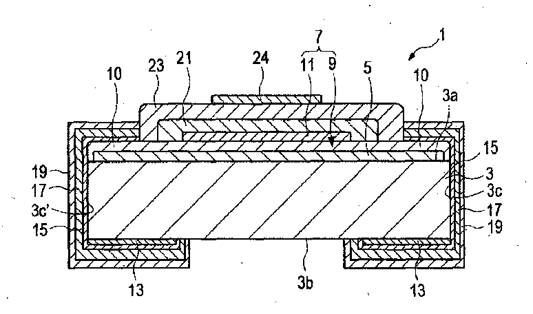
図1は本発明のチップヒューズの実施の形態の一例の断面図である。なお、理解を容易にするため、図1においては各部の厚み寸法を誇張して描いている。図1に示すように、このチップヒューズ1は、ほぼ矩形の絶縁性基板3を有している。本実施の形態では、チップ状の絶縁性基板3を、アルミナ基板(セラミック基板)により形成している。 Figure 1 is a cross-sectional view of one embodiment of the chip fuse of the present invention. Note that for ease of understanding, the thickness dimensions of each part are exaggerated in Figure 1. As shown in Figure 1, this chip fuse 1 has a substantially rectangular insulating substrate 3. In this embodiment, the chip-shaped insulating substrate 3 is formed from an alumina substrate (ceramic substrate).
絶縁性基板3の基板表面3aには、ガラスペーストを用いて絶縁性のアンダーコート5がスクリーン印刷により形成されている。アンダーコート5は、絶縁性基板3の長手方向の両端面に近い部分を除いて、基板表面3aのほぼ全体を覆っている。アンダーコート5の上には、ヒューズ素子7が形成されている。なおこのアンダーコート5は、電圧に応じて使用の可否を決定すればよく。必ず必要なものではない。本実施の形態のヒューズ素子7は、銅を主成分とする厚みが1μm~20μmのメッキ膜からなる第1の金属薄膜9と、第1の金属薄膜9の上に形成された錫を主成分とする厚みが0.5μm~10μmのメッキ膜からなる第2の金属薄膜11とから形成されている。第1の金属薄膜9の両端部分は、一対の表面電極10,10を構成している。言い換えると、本実施の形態のヒューズ素子7は、第2の金属薄膜11とその直下の第1の金属薄膜9の部分によって、構成されている。このような構成のヒューズ素子7は、溶断性能に優れ、且つ溶融金属の溜まりを形成し易いという性質を示すことが分かっている。On the substrate surface 3a of the insulating substrate 3, an insulating undercoat 5 is formed by screen printing using glass paste. The undercoat 5 covers almost the entire substrate surface 3a, except for the portions close to both ends of the insulating substrate 3 in the longitudinal direction. A fuse element 7 is formed on the undercoat 5. The undercoat 5 can be used or not depending on the voltage. It is not necessarily required. The fuse element 7 of this embodiment is formed from a first metal thin film 9 made of a plating film mainly composed of copper and having a thickness of 1 μm to 20 μm, and a second metal thin film 11 made of a plating film mainly composed of tin and having a thickness of 0.5 μm to 10 μm formed on the first metal thin film 9. Both ends of the first metal thin film 9 form a pair of surface electrodes 10, 10. In other words, the fuse element 7 of this embodiment is formed from the second metal thin film 11 and the portion of the first metal thin film 9 directly below it. It has been found that the fuse element 7 having such a configuration has excellent melting performance and exhibits the property of easily forming a pool of molten metal.
また絶縁性基板3の裏面3bの両端部分には、第1の金属薄膜9と同様の銅を主成分とする金属成分を含むメッキ膜からなる一対の裏面電極13,13が形成されている。 In addition, a pair of rear electrodes 13, 13 made of a plating film containing a metal component mainly composed of copper, similar to the first metal thin film 9, are formed on both ends of the rear surface 3b of the insulating substrate 3.
側面電極15,15は、ニッケルメッキ層(内部メッキ)17,17により全体的に覆われている。そしてニッケルメッキ層17,17は、Snのメッキ層19,19(外部メッキ)により全体的に覆われている。The side electrodes 15, 15 are entirely covered with nickel plating layers (internal plating) 17, 17. The nickel plating layers 17, 17 are entirely covered with Sn plating layers 19, 19 (external plating).
図2は、絶縁性基板3上にヒューズ素子7を形成する際に形成するL字形の2本のトリミング溝TSの形成例を示している。2本のトリミング溝TSは、一対の表面電極10,10とヒューズ素子7とに跨って形成されており、2本のトリミング溝TSの間に、実際のヒューズ素子7が形成される。図2において、符号25で指した領域が、ヒューズ素子7に遮断電流が流れたときに溶断する溶断部である。 Figure 2 shows an example of the formation of two L-shaped trimming grooves TS formed when forming a fuse element 7 on an insulating substrate 3. The two trimming grooves TS are formed across a pair of surface electrodes 10, 10 and the fuse element 7, and the actual fuse element 7 is formed between the two trimming grooves TS. In Figure 2, the area indicated by the symbol 25 is the fusion portion that melts when an interruption current flows through the fuse element 7.
さらに本実施の形態では、ヒューズ素子7の一部を構成する第2の金属薄膜11を全体的に覆うように厚膜により形成された絶縁性を有する高柔軟性の第1の保護膜21と、第1の保護膜21を覆うように厚膜により形成された、絶縁性を有する高硬度の第2の保護膜23を備えている。本実施の形態では、第1の保護膜21として高柔軟性のシリコーンゴムを用いている。第2の保護膜23は、第1の保護膜21を形成する高柔軟性のシリコーンゴムとの接合性及び保護特性を考慮して、高硬度のエポキシまたはシリコーン系の樹脂材料によって形成されている。第2の保護膜23の上には捺印24が印刷されている。 Furthermore, in this embodiment, a first protective film 21 having high flexibility and insulating properties is formed as a thick film so as to entirely cover the second thin metal film 11 constituting a part of the fuse element 7, and a second protective film 23 having high hardness and insulating properties is formed as a thick film so as to cover the first protective film 21. In this embodiment, a highly flexible silicone rubber is used as the first protective film 21. The second protective film 23 is formed of a highly hard epoxy or silicone-based resin material, taking into consideration the bonding property and protective properties with the highly flexible silicone rubber that forms the first protective film 21. A stamp 24 is printed on the second protective film 23.
本実施の形態では、第1の保護膜21を形成するシリコーンゴムとして、ヒューズ素子が溶断したときに、ヒューズ素子7の溶断部25(図2参照)の両側に金属薄膜の溶融金属の溜まり部が形成されることを可能にするせん断強度及びゴム硬度を有する高柔軟性のシリコーンゴムを用いている。第1の保護膜21及び第2の保護膜23は、それぞれスクリーン印刷により形成されている。第1の保護膜21は、第2の保護膜23を形成する際の焼成温度においても、高柔軟性は実質的に影響を受けることがないものである。In this embodiment, the silicone rubber forming the first protective film 21 is a highly flexible silicone rubber having a shear strength and rubber hardness that allows a pool of molten metal of the metal thin film to be formed on both sides of the fuse element 7's melting portion 25 (see FIG. 2) when the fuse element melts. The first protective film 21 and the second protective film 23 are each formed by screen printing. The high flexibility of the first protective film 21 is not substantially affected even at the baking temperature when the second protective film 23 is formed.
第1の保護膜21を形成する具体的なシリコーンゴムは、従来、消弧用として用いられているシリコーンゴムではなく、接着剤として用いられているシリコーンゴムの中で、ヒューズ素子が溶断したときに、アークの消弧性を発揮し且つヒューズ素子の溶断部の両側に金属薄膜の溶融金属の溜まり部を保持できるものである。本実施の形態で用いた具体的なシリコーンゴムは、接着材の材料として用いられるものの中で、せん断接着強度が3.1MPa以上3.9MPa以下であり且つデュロメータタイプAの硬度計で測定したゴム硬度が約66のシリコーンゴムである。従来のチップヒューズ素子で用いていたシリコーンゴムは、絶縁性基板とヒューズ素子長さの寸法が小さくなるほど、遮断時にアークが切れにくくなるが、本実施の形態で用いたシリコーンゴムは、ヒューズ素子の長さ寸法が小さくなったときでも、ヒューズ素子が溶断したときに、シリコーンゴム自身が消弧性能を発揮するとともに、ヒューズ素子の溶断部の両側に金属薄膜の溶融金属の溜まり部が形成された後に、その溜まり部を保持する機能がある。すなわち発明者は、ヒューズ素子とシリコーンゴムとを強く密着させることでシリコーンゴムの消弧効果を高くし、しかも溶融金属の溜まり部を保持する機能を高めることを可能にするせん断接着強度及びゴム硬度を有するシリコーンゴムを第1の保護膜に用いることにより、目的を達成できることを見出したのである。発明者は、寸法が小さい絶縁性基板を用いる場合において、遮断時のアークの発生を抑制するためには第1の保護膜の柔らかさと、ヒューズ素子及びその周囲にある基板面とシリコーンゴムとの密着性を高めることが重要であることを見出して本発明を完成したのである。本発明のように特定の性質を有する第1の保護膜を用いると、ヒューズ素子が溶断した後に、第1の保護膜が変形することによって、溶断部の両側に確実に金属薄膜の溶融溜まりが形成されて保持され、アークの発生と持続を抑制できる。The specific silicone rubber forming the first protective film 21 is not the silicone rubber conventionally used for arc extinguishing, but is a silicone rubber used as an adhesive that exhibits arc extinguishing properties when the fuse element melts and can hold a pool of molten metal of the metal thin film on both sides of the melted part of the fuse element. The specific silicone rubber used in this embodiment is a silicone rubber used as an adhesive material that has a shear adhesive strength of 3.1 MPa to 3.9 MPa and a rubber hardness of about 66 measured with a durometer type A hardness tester. The silicone rubber used in the conventional chip fuse element is such that the arc is less likely to be cut off when the insulating substrate and the fuse element length are smaller, but the silicone rubber used in this embodiment exhibits arc extinguishing properties when the fuse element melts, even when the length of the fuse element is smaller, and has the function of holding the pool after the pool of molten metal of the metal thin film is formed on both sides of the melted part of the fuse element. That is, the inventor found that the object can be achieved by using silicone rubber for the first protective film, which has a shear adhesion strength and rubber hardness that can enhance the arc-extinguishing effect of the silicone rubber by strongly adhering the fuse element and the silicone rubber, and also enhances the function of holding the pool of molten metal. The inventor found that in order to suppress the generation of an arc during interruption when using an insulating substrate with small dimensions, it is important to improve the softness of the first protective film and the adhesion between the fuse element and the substrate surface around it and the silicone rubber, and thus completed the present invention. When the first protective film having specific properties is used as in the present invention, after the fuse element melts, the first protective film deforms, and a molten pool of metal thin film is reliably formed and held on both sides of the melted part, thereby suppressing the generation and continuation of an arc.
なお、せん断接着強度は、理論的に上限はないものの、実用上入手可能なシリコーンゴムのせん断接着強度は5MPa以下であり、発明者が確認した好ましいせん断接着強度は3.1MPa以上3.9MPa以下であった。またデュロメータタイプAの硬度計で測定したゴム硬度は、柔らかいほど金属薄膜の溶断部の溶融溜まり部が広がり易く、硬いほど溶融溜まり部は広がり難くなる。発明者の研究によると、実用上入手可能なシリコーンゴムの中で、デュロメータタイプAの硬度計で測定したゴム硬度が約66のシリコーンゴムの硬度であれば、必要な溶融溜まり部の広がりと高い消弧効果を得ることができることを確認できた。なお第1の保護膜21の厚みは、10μm~50μmであれば、本発明の効果が得られることも発明者は確認した。これらの特性を有するシリコーンゴムであれば、第1の保護膜21に必要な変形を可能にすることができる。これらの数値は、試験を行うことによって確認されたものであり、実用上の観点から決定された。Although there is no theoretical upper limit to the shear adhesive strength, the shear adhesive strength of silicone rubber available in practice is 5 MPa or less, and the preferred shear adhesive strength confirmed by the inventor is 3.1 MPa or more and 3.9 MPa or less. The softer the rubber hardness measured with a durometer type A hardness tester, the easier it is for the molten pool of the fused part of the metal thin film to spread, and the harder it is, the harder the molten pool spreads. According to the inventor's research, it was confirmed that among the silicone rubbers available in practice, if the silicone rubber has a rubber hardness measured with a durometer type A hardness tester of about 66, the necessary molten pool spread and a high arc-extinguishing effect can be obtained. The inventor also confirmed that the effect of the present invention can be obtained if the thickness of the first protective film 21 is 10 μm to 50 μm. If the silicone rubber has these characteristics, it is possible to make the necessary deformation of the first protective film 21. These values were confirmed by conducting tests and were determined from a practical viewpoint.
図3は、本実施の形態の実施例1及び2で用いる第1の保護膜21に利用可能なシリコーンゴムを選択するためにシリコーン材料のメーカから入手したシリコーンゴムの特性と、第1の保護膜21としてその他のシリコーンゴムを用いる比較例1乃至3で用いるシリコーンゴムの特性を示すものである。比較例1乃至3のシリコーンゴムも接着剤として用いるものである。 Figure 3 shows the characteristics of silicone rubber obtained from a silicone material manufacturer to select silicone rubber usable for the first protective film 21 used in Examples 1 and 2 of this embodiment, and the characteristics of silicone rubber used in Comparative Examples 1 to 3, which use other silicone rubber as the first protective film 21. The silicone rubbers in Comparative Examples 1 to 3 are also used as adhesives.
図3のシリコーンゴムを用いた実施例1及び2及び比較例1乃至3においては、長さ寸法が2.0mmで且つ幅寸法が1.2mmのセラミック基板からなる絶縁性基板3を用いた。そして銅を主成分する厚みが5μmのメッキ膜からなる第1の金属薄膜9と、第1の金属薄膜9の上に錫を主成分とする厚みが1μmのメッキ膜からなる第2の金属薄膜11からなるヒューズ素子7を構成した。また実施例1及び2で用いた第1の保護膜21は、せん断接着強度が3.1MPaと3.9MPaであり且つデュロメータタイプAの硬度計で測定したゴム硬度が約66のシリコーンゴムであった。第1の保護膜21の厚みは約30μmであった。更に第1の保護膜21を覆うように、硬度3Hのシリコーン系の樹脂材料により形成された厚みが80μmの第2の保護膜23を形成した。そして比較例1乃至3のチップヒューズについては、第1の保護膜21を形成するシリコーンゴムの材質を除いては、実施例1及び2と同じ構成で製造した。In Examples 1 and 2 and Comparative Examples 1 to 3 using the silicone rubber of FIG. 3, an insulating substrate 3 was used, which was a ceramic substrate having a length of 2.0 mm and a width of 1.2 mm. A fuse element 7 was formed, which was composed of a first metal thin film 9 made of a plating film mainly composed of copper and having a thickness of 5 μm, and a second metal thin film 11 made of a plating film mainly composed of tin and having a thickness of 1 μm on the first metal thin film 9. The first protective film 21 used in Examples 1 and 2 was silicone rubber having shear adhesive strengths of 3.1 MPa and 3.9 MPa and a rubber hardness of about 66 measured with a durometer type A hardness tester. The thickness of the first protective film 21 was about 30 μm. A second protective film 23 was formed to cover the first protective film 21, and was made of a silicone-based resin material having a hardness of 3H and a thickness of 80 μm. The chip fuses of Comparative Examples 1 to 3 were manufactured in the same configuration as Examples 1 and 2, except for the silicone rubber material that formed the first protective film 21.
図4は、実施例1及び2並びに比較例1乃至3の構成で定格電流が1.25Aのチップヒューズを作り、これらのチップヒューズについて行った遮断容量試験の試験結果を示している。この試験結果では、溶断電流を4Aとして、100Vから200Vの回復電圧が印加されたときに、実施例1及び2と比較例1乃至3のチップヒューズがアークの持続によって焼損する確率を確認した。その結果、実施例1及び2のチップヒューズでは、実質的にアークの発生はなかった。特に、実施例1及び2のチップヒューズでは、定格電圧75Vで、最大遮断電流が50Aの遮断特性が得られることが確認された。これに対して、比較例1乃至3のチップヒューズでは、同じ条件で遮断容量試験を行った結果、焼損に結びつくアークが発生することを確認した。 Figure 4 shows the results of a breaking capacity test performed on chip fuses with a rated current of 1.25 A made with the configurations of Examples 1 and 2 and Comparative Examples 1 to 3. In this test, the probability of the chip fuses of Examples 1 and 2 and Comparative Examples 1 to 3 burning out due to a sustained arc was confirmed when a recovery voltage of 100 V to 200 V was applied with a melting current of 4 A. As a result, there was practically no arc generation in the chip fuses of Examples 1 and 2. In particular, it was confirmed that the chip fuses of Examples 1 and 2 have a breaking characteristic of a maximum breaking current of 50 A at a rated voltage of 75 V. In contrast, the chip fuses of Comparative Examples 1 to 3 were subjected to a breaking capacity test under the same conditions, and it was confirmed that an arc leading to burning out was generated.
なお第2の保護膜23の材料は、特に限定されないが、シリコーンゴムとの接合性及び保護特性を考慮すると、厚みが10μm~100μmのエポキシまたはシリコーン系の樹脂材料によって形成されているのが望ましいことも発明者の試験により確認されている。The material of the second protective film 23 is not particularly limited, but the inventors' tests have confirmed that, taking into consideration the bonding properties with silicone rubber and the protective properties, it is desirable for the film to be formed from an epoxy or silicone-based resin material with a thickness of 10 μm to 100 μm.
本発明によれば、第1の保護膜を形成するシリコーンゴムとして、ヒューズ素子が溶断したときに、ヒューズ素子の溶断部の両側に金属薄膜の溶融金属の溜まり部が形成されることを可能にするゴム硬度及びせん断接着強度を有するものを用いることにより、ヒューズ素子が溶断した後に、第1の保護膜が変形することによって、溶断部の両側に確実に金属薄膜の溶融溜まりが形成され、ヒューズ素子と強く密着させることでシリコーンゴムの消弧効果を高く維持して、アークの発生を抑制できる長さ寸法が2.0mm以下で且つ幅寸法が1.2mm以下のセラミック基板等の絶縁性基板を用いたチップヒューズを提供できる。According to the present invention, by using silicone rubber for forming the first protective film that has a rubber hardness and shear adhesion strength that enables pools of molten metal from the metal thin film to be formed on both sides of the fusion portion of the fuse element when the fuse element melts, the first protective film deforms after the fuse element melts, reliably forming pools of molten metal from the metal thin film on both sides of the fusion portion, and by strongly adhering to the fuse element, the arc-extinguishing effect of the silicone rubber is maintained at a high level, thereby providing a chip fuse that uses an insulating substrate such as a ceramic substrate with a length dimension of 2.0 mm or less and a width dimension of 1.2 mm or less that can suppress the generation of an arc.
1 チップヒューズ
3 絶縁性基板
5 アンダーコート
7 ヒューズ素子
9 第1の金属薄膜
10 表面電極
11 第2の金属薄
13 裏面電極
15 側面電極
17 内部メッキ
19 外部メッキ
21 第1の保護膜
23 第2の保護膜
24 捺印
25 溶断部
REFERENCE SIGNS LIST 1 chip fuse 3 insulating substrate 5 undercoat 7 fuse element 9 first metal thin film 10 surface electrode 11 second metal thin film 13 back electrode 15 side electrode 17 internal plating 19 external plating 21 first protective film 23 second protective film 24 marking 25 fusion portion
Claims (7)
前記絶縁性基板の上に金属薄膜により形成されたヒューズ素子と、
せん断接着強度が3.1MPa以上3.9MPa以下であり且つデュロメータタイプAの硬度計で測定したゴム硬度が約66のシリコーンゴムにより、前記ヒューズ素子を覆うように形成された第1の保護膜と、
前記第1の保護膜を覆うように、樹脂材料により形成された第2の保護膜とを備えていることを特徴とするチップヒューズ。 an insulating substrate made of a ceramic substrate having a length dimension of 2.0 mm or less and a width dimension of 1.2 mm or less;
a fuse element formed of a metal thin film on the insulating substrate;
a first protective film formed to cover the fuse element and made of silicone rubber having a shear adhesive strength of 3.1 MPa to 3.9 MPa and a rubber hardness of about 66 as measured by a durometer type A hardness tester;
a second protective film formed of a resin material so as to cover the first protective film.
前記ヒューズ素子は前記アンダーコートの上に形成されている請求項1または2に記載のチップヒューズ。 an insulating undercoat is formed on the insulating substrate;
3. The chip fuse according to claim 1, wherein the fuse element is formed on the undercoat.
前記絶縁性基板の上に金属薄膜により形成されたヒューズ素子と、
前記ヒューズ素子を覆うように厚膜により形成された、絶縁性を有する第1の保護膜と、
前記第1の保護膜を覆うように厚膜により形成された、絶縁性を有する第2の保護膜を備えたチップヒューズにおいて、
前記第1の保護膜としてシリコーンゴムが用いられ、
前記シリコーンゴムとして、前記ヒューズ素子が溶断したときに、アークの消弧性を発揮し且つ前記ヒューズ素子の溶断部の両側に前記金属薄膜の溶融金属の溜まり部を保持できるせん断接着強度及びゴム硬度を有するものが用いられていることを特徴とするチップヒューズ。 an insulating substrate such as a ceramic substrate having a length dimension of 2.0 mm or less and a width dimension of 1.2 mm or less;
a fuse element formed of a metal thin film on the insulating substrate;
a first protective film having insulating properties and formed of a thick film so as to cover the fuse element;
A chip fuse including a second protective film having insulating properties and formed of a thick film so as to cover the first protective film,
Silicone rubber is used as the first protective film,
A chip fuse, characterized in that the silicone rubber used has a shear adhesive strength and rubber hardness sufficient to extinguish an arc when the fuse element melts and to hold reservoirs of molten metal in the metal thin film on both sides of the melted portion of the fuse element.
Applications Claiming Priority (3)
| Application Number | Priority Date | Filing Date | Title |
|---|---|---|---|
| JP2021186471 | 2021-11-16 | ||
| JP2021186471 | 2021-11-16 | ||
| JP2022042398 | 2022-11-15 |
Publications (1)
| Publication Number | Publication Date |
|---|---|
| JP3248564U true JP3248564U (en) | 2024-10-03 |
Family
ID=92902674
Family Applications (1)
| Application Number | Title | Priority Date | Filing Date |
|---|---|---|---|
| JP2024600091U Active JP3248564U (en) | 2021-11-16 | 2022-11-15 | Chip fuse |
Country Status (1)
| Country | Link |
|---|---|
| JP (1) | JP3248564U (en) |
-
2022
- 2022-11-15 JP JP2024600091U patent/JP3248564U/en active Active
Similar Documents
| Publication | Publication Date | Title |
|---|---|---|
| TWI398894B (en) | Protection element | |
| US8767368B2 (en) | Protective element and method for producing the same | |
| US20100134235A1 (en) | Esd protector and method of manufacturing the same | |
| EP1041597A2 (en) | Protective device | |
| JP2004214033A (en) | Protection element | |
| US20220199346A1 (en) | Protective element | |
| JP2004265617A (en) | Protective element | |
| TWI500063B (en) | Circuit protection device including resistor and fuse element | |
| CN107359033A (en) | Chip resistor and manufacturing method thereof | |
| WO2006030705A1 (en) | Chip-shaped electronic part | |
| WO2011043233A1 (en) | Chip fuse | |
| US10763018B2 (en) | Chip resistor | |
| WO2023090320A1 (en) | Chip fuse | |
| JPH09306319A (en) | Overvoltage-overcurrent protective device | |
| JP4037248B2 (en) | Circuit protection element and manufacturing method thereof | |
| JP2013197002A (en) | Circuit protection element | |
| JP2001345035A (en) | Protecting element | |
| CN204167243U (en) | Circuit protecting element | |
| JP3853418B2 (en) | Overvoltage / overcurrent protection device | |
| JPH10308160A (en) | fuse | |
| JPH09306317A (en) | Overvoltage-overcurrent protective device | |
| CN116569286A (en) | Chip Resistors | |
| JP2014096272A (en) | Circuit protection element | |
| JP2001222938A (en) | Protection element | |
| JPH10308161A (en) | fuse |
Legal Events
| Date | Code | Title | Description |
|---|---|---|---|
| R150 | Certificate of patent or registration of utility model |
Ref document number: 3248564 Country of ref document: JP Free format text: JAPANESE INTERMEDIATE CODE: R150 |