JP3141579U - LED lighting fixtures - Google Patents
LED lighting fixtures Download PDFInfo
- Publication number
- JP3141579U JP3141579U JP2008001075U JP2008001075U JP3141579U JP 3141579 U JP3141579 U JP 3141579U JP 2008001075 U JP2008001075 U JP 2008001075U JP 2008001075 U JP2008001075 U JP 2008001075U JP 3141579 U JP3141579 U JP 3141579U
- Authority
- JP
- Japan
- Prior art keywords
- substrate
- ceiling
- led lighting
- board
- lighting apparatus
- Prior art date
- Legal status (The legal status is an assumption and is not a legal conclusion. Google has not performed a legal analysis and makes no representation as to the accuracy of the status listed.)
- Expired - Fee Related
Links
Images


Classifications
-
- F—MECHANICAL ENGINEERING; LIGHTING; HEATING; WEAPONS; BLASTING
- F21—LIGHTING
- F21K—NON-ELECTRIC LIGHT SOURCES USING LUMINESCENCE; LIGHT SOURCES USING ELECTROCHEMILUMINESCENCE; LIGHT SOURCES USING CHARGES OF COMBUSTIBLE MATERIAL; LIGHT SOURCES USING SEMICONDUCTOR DEVICES AS LIGHT-GENERATING ELEMENTS; LIGHT SOURCES NOT OTHERWISE PROVIDED FOR
- F21K9/00—Light sources using semiconductor devices as light-generating elements, e.g. using light-emitting diodes [LED] or lasers
- F21K9/20—Light sources comprising attachment means
- F21K9/23—Retrofit light sources for lighting devices with a single fitting for each light source, e.g. for substitution of incandescent lamps with bayonet or threaded fittings
- F21K9/232—Retrofit light sources for lighting devices with a single fitting for each light source, e.g. for substitution of incandescent lamps with bayonet or threaded fittings specially adapted for generating an essentially omnidirectional light distribution, e.g. with a glass bulb
-
- F—MECHANICAL ENGINEERING; LIGHTING; HEATING; WEAPONS; BLASTING
- F21—LIGHTING
- F21V—FUNCTIONAL FEATURES OR DETAILS OF LIGHTING DEVICES OR SYSTEMS THEREOF; STRUCTURAL COMBINATIONS OF LIGHTING DEVICES WITH OTHER ARTICLES, NOT OTHERWISE PROVIDED FOR
- F21V3/00—Globes; Bowls; Cover glasses
-
- F—MECHANICAL ENGINEERING; LIGHTING; HEATING; WEAPONS; BLASTING
- F21—LIGHTING
- F21Y—INDEXING SCHEME ASSOCIATED WITH SUBCLASSES F21K, F21L, F21S and F21V, RELATING TO THE FORM OR THE KIND OF THE LIGHT SOURCES OR OF THE COLOUR OF THE LIGHT EMITTED
- F21Y2107/00—Light sources with three-dimensionally disposed light-generating elements
- F21Y2107/40—Light sources with three-dimensionally disposed light-generating elements on the sides of polyhedrons, e.g. cubes or pyramids
-
- F—MECHANICAL ENGINEERING; LIGHTING; HEATING; WEAPONS; BLASTING
- F21—LIGHTING
- F21Y—INDEXING SCHEME ASSOCIATED WITH SUBCLASSES F21K, F21L, F21S and F21V, RELATING TO THE FORM OR THE KIND OF THE LIGHT SOURCES OR OF THE COLOUR OF THE LIGHT EMITTED
- F21Y2115/00—Light-generating elements of semiconductor light sources
- F21Y2115/10—Light-emitting diodes [LED]
Landscapes
- Engineering & Computer Science (AREA)
- Physics & Mathematics (AREA)
- Microelectronics & Electronic Packaging (AREA)
- Optics & Photonics (AREA)
- General Engineering & Computer Science (AREA)
- Fastening Of Light Sources Or Lamp Holders (AREA)
- Non-Portable Lighting Devices Or Systems Thereof (AREA)
Abstract
【課題】低消費電力タイプのチップLEDを用いて所望の輝度を確保することのできるLED照明器具を提供する。
【解決手段】基板構造体の複数の側面基板と天井基板の各々に複数のチップLEDが実装されている。側面基板及び天井基板の互いに隣接するチップLEDで挟まれたほぼ全領域に回路パターンが設けられ、回路パターンの一部を構成する配線導体16が側面基板及び天井基板の縁まで延びて、互いに隣接する側面基板及び/又は天井基板の縁に位置する配線導体16を半田付けにより接続することにより各チップLEDが電気的に接続されると共に側面基板及び天井基板が互いに固定される。
【選択図】図5An LED lighting apparatus capable of ensuring a desired luminance using a low power consumption type chip LED is provided.
A plurality of chip LEDs are mounted on each of a plurality of side substrates and a ceiling substrate of a substrate structure. A circuit pattern is provided in almost the entire region sandwiched between the chip LEDs adjacent to each other on the side board and the ceiling board, and the wiring conductor 16 constituting a part of the circuit pattern extends to the edge of the side board and the ceiling board and is adjacent to each other. By connecting the wiring conductors 16 positioned at the edges of the side board and / or the ceiling board to be connected by soldering, the respective chip LEDs are electrically connected and the side board and the ceiling board are fixed to each other.
[Selection] Figure 5
Description
本発明は、多数のチップLEDを光源とするLED照明器具に関する。 The present invention relates to an LED lighting apparatus using a large number of chip LEDs as light sources.
LED(Light Emitting Diode)は既に様々な分野で活用されているが、白色LEDが実用化された今日、白熱灯や蛍光灯に代わる照明器具として検討されている。LEDは白熱灯や蛍光灯に比べて長寿命であり且つ消費エネルギーも少ないため、地球温暖化が叫ばれている今日、LEDを採用した照明器具が普及する傾向にある。 LEDs (Light Emitting Diodes) have already been used in various fields, but today, when white LEDs are put into practical use, they are being considered as lighting fixtures that can replace incandescent and fluorescent lamps. Since LEDs have a longer life and consume less energy than incandescent lamps and fluorescent lamps, lighting fixtures that employ LEDs tend to become popular today when global warming is screaming.
特許文献1は、複数のLEDを配置した照明基板を同一平面上に複数配置した照明器具を提案している。また、特許文献2は、汎用ソケットに螺合可能な口金を備え、半球状の保持ユニットに複数のLED素子を装着した照明器具を提案している。より具体的には、特許文献2は、LED素子は、プラス及びマイナスの脚端子が同軸上に上下に設けられ、他方、半球状の保持ユニットには、絶縁層を介して極性の異なる2つ送電皮膜が設けられ、各LED素子の脚端子を保持ユニットに挿入することで各LED素子に電源が供給されるようになっている。
ところで、現在入手可能なLEDは、超輝度タイプ、高輝度タイプ、低消費電力タイプなどに分類して製造販売され、また、形状として、砲弾型LED、表面実装型LED(チップLED)などに分類して製造販売されている。 By the way, currently available LEDs are classified and manufactured as super-brightness type, high-brightness type, low power consumption type, etc., and the shape is classified into bullet type LED, surface mount type LED (chip LED), etc. Are manufactured and sold.
LED照明の場合、大電流を使用する超高輝度LEDや高輝度LEDを利用すれば、所望の輝度のLED照明器具を作るのにLEDの使用数は少なくてすむが、発熱対策と価格に難点がある。また、砲弾型LEDを採用するとLED照明器具の小型化に難点がある。 In the case of LED lighting, if you use ultra-bright LEDs or high-brightness LEDs that use a large current, you can use fewer LEDs to make LED lighting fixtures with the desired brightness. There is. In addition, when a bullet-type LED is employed, there is a difficulty in miniaturizing the LED lighting apparatus.
本考案の目的は、低消費電力タイプのチップLEDを用いて所望の輝度を確保することのできるLED照明器具を提供することにある。 The objective of this invention is providing the LED lighting fixture which can ensure desired brightness | luminance using the low power consumption type chip | tip LED.
本発明の更なる目的は、小型チップLEDの配線、組立を効率化することのできるLED照明器具を提供することにある。 It is a further object of the present invention to provide an LED lighting apparatus that can improve the efficiency of wiring and assembly of small chip LEDs.
上記の技術的課題は、本発明によれば、
多角柱状又は切頭多角錐状の基板構造体の側面を構成する複数の側面基板と、前記多角柱状又は切頭多角錐状の基板構造体の天井面を構成する多角形の天井基板の各々に複数のチップLEDが実装されていることを特徴とするLED照明器具を提供することにより達成される。
According to the present invention, the above technical problem is
A plurality of side substrates constituting the side surface of the polygonal columnar or truncated polygonal pyramid substrate structure, and a polygonal ceiling substrate constituting the ceiling surface of the polygonal columnar or truncated polygonal pyramid substrate structure This is achieved by providing an LED luminaire characterized in that a plurality of chip LEDs are mounted.
本発明の好ましい実施の形態によれば、チップLEDを複数個搭載した側面基板及び天井基板の組合せにより多角柱を構成し、数多くのLEDを立体的に配置する。また、側面基板と天井基板の構造的固定と電気的接続は、各基板の縁に設けた配線導体の半田付けを行うことにより同時に行う。 According to a preferred embodiment of the present invention, a polygonal column is formed by a combination of a side substrate and a ceiling substrate on which a plurality of chip LEDs are mounted, and a large number of LEDs are arranged three-dimensionally. Further, the structural fixing and electrical connection between the side board and the ceiling board are simultaneously performed by soldering the wiring conductors provided on the edges of the respective boards.
また、側面基板及び天井基板の回路パターンを極力大きく設定すると共に回路パターンを側面基板及び天井基板の表面と裏面に設けて、この両面の回路パターンを接続してLEDが発する熱を各基板の表面の回路パターンだけでなく裏面の回路パターンを使って放熱できるため放熱効果を向上させることができる。 Also, the circuit patterns of the side board and the ceiling board are set as large as possible, and the circuit patterns are provided on the front and back surfaces of the side board and the ceiling board, and the heat generated by the LEDs is generated by connecting the circuit patterns on both sides. Since heat can be radiated using not only the circuit pattern but also the circuit pattern on the back surface, the heat radiation effect can be improved.
また、側面基板及び天井基板の表面の回路パターンの表面にメッキ処理を施して反射鏡の機能を付与することで、LEDが発する光を効率的に照明に寄与させる。 Moreover, the surface of the circuit pattern on the surface of the side board and the ceiling board is plated to give the function of a reflecting mirror, so that the light emitted from the LED can efficiently contribute to illumination.
多角柱又は切頭多角錐の基板構造体を構成する側面基板及び天井基板は、これらをVカット加工して面付けした基板から切り離すことで形成され、そして、このVカット加工のライン上に長孔状の透孔を設けて、この透孔の周縁に配線導体を設けることで、この透孔の部分を半田付けすることで、互いに隣接する側面基板同士及び天井基板と側面基板とが固定されると共に各LEDが電気的に接続される。勿論、Vカット加工により面付けする基板に対してチップLEDを作業ロボットにより実装することができる。また、従来ならば反射板は別部品となるが、本考案では基板自体が反射板の役目も果たす。 The side substrate and the ceiling substrate constituting the substrate structure of the polygonal column or the truncated polygonal pyramid are formed by separating them from the substrate that has been subjected to V-cut processing and imposing, and long on the V-cut processing line. By providing a hole-shaped through-hole and providing a wiring conductor at the periphery of the through-hole, by soldering the through-hole portion, the side boards adjacent to each other and the ceiling board and the side board are fixed. In addition, each LED is electrically connected. Of course, the chip LED can be mounted on the substrate to be impositioned by V-cut processing by the work robot. In addition, the reflection plate is a separate component in the past, but in the present invention, the substrate itself also serves as the reflection plate.
図1は実施例の電球型LED照明器具を示す。図1を参照して、電球型LED照明器具1は、電極口金2を有し、この電極口金2を汎用のソケットに螺合することにより商用電源を使って照明することができる。
FIG. 1 shows a light bulb type LED lighting apparatus of the embodiment. Referring to FIG. 1, a light bulb type
電球型LED照明器具1は電極口金2の近傍に配設された不透明プラスチックケース3を有し、このプラスチックケース3内に電源回路(図示せず)が収容されている。不透明プラスチックケース3の上方に光透過性のカバー4が設けられ、このカバー4内に、基板構造体5が収容されている。光透過性カバー4は、プラスチック製であってもよいしガラス製であってもよい。
The bulb-type
図2は、電球型LED照明器具1から光透過性カバー4を取り除いて基板構造体5を露出させた図である。図2を参照して、基板構造体5は、六枚の側面基板6と、一枚の天井基板7とで構成された六角柱の形状を有しており、各基板6、7には複数のチップLED10が配列されている。ここに、チップLED10は比較的低輝度の低消費電力タイプのLEDが採用される。
FIG. 2 is a view in which the
側面基板6は、長方形の形状を有し、その長手方向に四個のチップLED10が直列に且つ互いに間隔を隔てて実装されている。また、天井基板7は平面視六角形の形状を有し、この天井基板7に三個のチップLED10が直列に且つ互いに間隔を隔てて実装されている。なお、六角柱は例示に過ぎず、四角形、五角形、八角形などの多角柱の形状を任意に採用することができる。勿論、多角形の天井面を備えた切頭多角錐の形状を採用してもよい。
The
上述した複数の側面基板6が一枚の基板11に面付けされ、そして、側面基板6が分離される前の状態を図3に示す。なお、同じ一枚の基板11に天井基板7を含めて面付けしてもよいし、この天板基板7については別の基板に面付けしてもよい。
FIG. 3 shows a state before the plurality of
図3を参照して、基板11には、縦線12と横線13によって複数の側面基板6が区分され、縦線12及び横線13に沿って切断することにより各側面基板6を形成することができる。ここに、縦線12と横線13は断面V字状のVカット加工が施されている。縦線12、横線13には、長孔形状の透孔14を有する。図3の参照符号15は回路パターンを示す。この回路パターン15は、隣接するチップLED10、10を電気的に接続するものであり、図3から理解できるように、各側面基板6の隣接するチップLED10、10の間のほぼ全領域を使って回路パターン15が形成されている。そして、このチップLED10及び回路パターン15が設けられている側面基端6の表面には、ニッケルなどの光反射メッキが施されている。また、基板11の表面を保護するレジスト塗料として透明な材料が採用され、これにより回路パターン15は反射鏡の機能が付与されている。天井基板7についても、側面基板6と実質的に同じ構成が採用されている。
Referring to FIG. 3, a plurality of
上記の長孔形状の透孔14のうち、適宜の透孔14には、図4に示すように、透孔14の周縁部にも配線導体16が塗布され、配線導体16によって隣接する側面基板6及び天井基板7が互いに電気的に接続される。
As shown in FIG. 4, among the long hole-shaped through
側面基板6及び天井基板7の裏面には、上述した回路パターン15及び配線導体16と同じ導電性材料が塗布されている(図示せず)。そして、側面基板6及び天井基板7の表と裏の回路パターン15及び配線導体16は透孔14の部位で互いに半田付けにより接続されている。これにより、チップLED10が発する熱は、基板6、7の両面においてチップLED10、10間のほぼ全領域に塗布された導電性材料からなる回路パターン15を使って効率的に放熱することができる。
The same conductive material as that of the
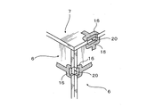
図5は基板11から切り離した各面の基板6、7の組立を示し、各面の基板6、7の回路パターン15は、透孔14の周縁部の配線導体16を半田付けすることにより電気的に接続される。半田付けする部位を参照符号20で示してある。
FIG. 5 shows the assembly of the
実施例のLED照明器具1によれば、複数のチップLED10を実装した側面基板6及び天井基板7を透孔14の周縁部の配線基板16を半田付けすることにより、各基板6、7のLED10を電気的に接続し且つ電源回路にも接続されるだけでなく、天井基板7及び複数の側面基板6同士が互いに固定されて構造的に一体化された六角柱の発光源となる。したがって、多数のチップLED10を組み込んだ基板構造体5の組立作業を効率化することができる。
According to the
また、実施例のLED照明器具1によれば、側面基板6及び天井基板7の表面において互いに隣接するチップLED10、10間のほぼ全領域を使って回路パターン15が形成されており、また、裏面においても回路パターン15と同様に導電性材料が塗布されており、導電性材料は一般的に熱伝導性が優れているため、LEDが発生した熱を基板構造体5の側面基板6及び天井基板7の表面及び裏面のほぼ全領域を使って効率的に放熱することができる。
Further, according to the
また、多角柱の基板構造体6各側面及び天井に数多くのチップLED10を配設することができるだけでなく、チップLED10が発する光は、反射鏡として機能する回路パターン15によって反射され、チップLED10が発する光を効率的に照明に寄与させることができる。
In addition, a large number of
1 電球型LED照明器具
2 電極口金
5 基板構造体
6 側面基板
7 天井基板
10 チップLED
11 面付けした基板
12、13 Vカット加工ライン
14 透孔
15 回路パターン
16 配線導体
20 半田付けする部位
DESCRIPTION OF
DESCRIPTION OF
Claims (7)
Priority Applications (1)
| Application Number | Priority Date | Filing Date | Title |
|---|---|---|---|
| JP2008001075U JP3141579U (en) | 2008-02-27 | 2008-02-27 | LED lighting fixtures |
Applications Claiming Priority (1)
| Application Number | Priority Date | Filing Date | Title |
|---|---|---|---|
| JP2008001075U JP3141579U (en) | 2008-02-27 | 2008-02-27 | LED lighting fixtures |
Publications (1)
| Publication Number | Publication Date |
|---|---|
| JP3141579U true JP3141579U (en) | 2008-05-08 |
Family
ID=43291632
Family Applications (1)
| Application Number | Title | Priority Date | Filing Date |
|---|---|---|---|
| JP2008001075U Expired - Fee Related JP3141579U (en) | 2008-02-27 | 2008-02-27 | LED lighting fixtures |
Country Status (1)
| Country | Link |
|---|---|
| JP (1) | JP3141579U (en) |
Cited By (11)
| Publication number | Priority date | Publication date | Assignee | Title |
|---|---|---|---|---|
| WO2010053147A1 (en) * | 2008-11-06 | 2010-05-14 | ローム株式会社 | Led lamp |
| JP2010141290A (en) * | 2008-12-11 | 2010-06-24 | Advance Connectek Inc | Light emitting diode light source module |
| WO2010117027A1 (en) * | 2009-04-10 | 2010-10-14 | 東芝ライテック株式会社 | Light emitting module and lighting apparatus |
| JP2011040364A (en) * | 2009-07-16 | 2011-02-24 | Pearl Lighting Co Ltd | Led lamp |
| JP2011054577A (en) * | 2008-11-06 | 2011-03-17 | Rohm Co Ltd | Led lamp |
| JP2011070986A (en) * | 2009-09-28 | 2011-04-07 | Wu Tsu Yao | Improvement of led light heat-radiation structure |
| BE1018931A5 (en) * | 2008-08-26 | 2011-11-08 | Stephane Verstraete | ILLUMINATION DEVICE AND IN PARTICULAR BULB OR TUBE FOR LED LAMP (LED). |
| JP2011243512A (en) * | 2010-05-20 | 2011-12-01 | Birumen Kagoshima:Kk | Led lighting tool |
| JP2012181953A (en) * | 2011-02-28 | 2012-09-20 | Toshiba Corp | Lighting system |
| JP2013191424A (en) * | 2012-03-14 | 2013-09-26 | Formolight Technologies Inc | Reflection type high ceiling light |
| WO2022028022A1 (en) * | 2020-08-04 | 2022-02-10 | 东莞市瑞拓科技有限公司 | Novel led stereoscopic light source |
-
2008
- 2008-02-27 JP JP2008001075U patent/JP3141579U/en not_active Expired - Fee Related
Cited By (12)
| Publication number | Priority date | Publication date | Assignee | Title |
|---|---|---|---|---|
| BE1018931A5 (en) * | 2008-08-26 | 2011-11-08 | Stephane Verstraete | ILLUMINATION DEVICE AND IN PARTICULAR BULB OR TUBE FOR LED LAMP (LED). |
| WO2010053147A1 (en) * | 2008-11-06 | 2010-05-14 | ローム株式会社 | Led lamp |
| JP2011054577A (en) * | 2008-11-06 | 2011-03-17 | Rohm Co Ltd | Led lamp |
| JP2010141290A (en) * | 2008-12-11 | 2010-06-24 | Advance Connectek Inc | Light emitting diode light source module |
| WO2010117027A1 (en) * | 2009-04-10 | 2010-10-14 | 東芝ライテック株式会社 | Light emitting module and lighting apparatus |
| US8439521B2 (en) | 2009-04-10 | 2013-05-14 | Toshiba Lighting & Technology Corporation | Light-emitting module and luminaire |
| JP2011040364A (en) * | 2009-07-16 | 2011-02-24 | Pearl Lighting Co Ltd | Led lamp |
| JP2011070986A (en) * | 2009-09-28 | 2011-04-07 | Wu Tsu Yao | Improvement of led light heat-radiation structure |
| JP2011243512A (en) * | 2010-05-20 | 2011-12-01 | Birumen Kagoshima:Kk | Led lighting tool |
| JP2012181953A (en) * | 2011-02-28 | 2012-09-20 | Toshiba Corp | Lighting system |
| JP2013191424A (en) * | 2012-03-14 | 2013-09-26 | Formolight Technologies Inc | Reflection type high ceiling light |
| WO2022028022A1 (en) * | 2020-08-04 | 2022-02-10 | 东莞市瑞拓科技有限公司 | Novel led stereoscopic light source |
Similar Documents
| Publication | Publication Date | Title |
|---|---|---|
| JP3141579U (en) | LED lighting fixtures | |
| JP2009277586A (en) | Electric lamp type led luminaire | |
| US8556462B2 (en) | LED lighting device | |
| CN100573939C (en) | The LED illuminating lamp of LED unit and use LED unit | |
| JP3171487U (en) | LED lighting device | |
| EP2392851A1 (en) | LED lighting device | |
| US9228724B2 (en) | Modular LED lamp structure with replaceable modules | |
| EP2261550A2 (en) | Knock-down led lighting fixtures | |
| US20050078477A1 (en) | Light emitting diode lamp | |
| US20130279164A1 (en) | Led lighting fixtures | |
| TW201317502A (en) | Light bar structure | |
| WO2017124784A1 (en) | Wide-angle light emitting led filament lamp | |
| KR100828299B1 (en) | An easy detachable light emitting diode lamp and socket | |
| CN102278612A (en) | Light emitting diode (LED) illumination lamp | |
| JP3163443U (en) | LED lighting device | |
| JP2016512921A (en) | LED lighting device | |
| US8833976B2 (en) | LED lighting device | |
| US20130062631A1 (en) | Light emitting structure, light emitting module, and light emitting device | |
| EP2354629A1 (en) | LED lamp for wide area lighting | |
| US20150009662A1 (en) | Light-Emitting Module and Luminaire | |
| KR20100044632A (en) | Lighting apparatus having led and circuit module therefor | |
| JP2011096649A (en) | Illumination device | |
| US20170097125A1 (en) | Light-emitting diode (led) lighting fixture solutions and methods | |
| US20110181164A1 (en) | Led lamp for wide area lighting | |
| JP2013201041A (en) | Light-emitting module, lighting device, and lighting fixture |
Legal Events
| Date | Code | Title | Description |
|---|---|---|---|
| R150 | Certificate of patent or registration of utility model |
Free format text: JAPANESE INTERMEDIATE CODE: R150 |
|
| FPAY | Renewal fee payment (event date is renewal date of database) |
Free format text: PAYMENT UNTIL: 20110416 Year of fee payment: 3 |
|
| LAPS | Cancellation because of no payment of annual fees |