JP3112546U - Semiconductor device package - Google Patents
Semiconductor device package Download PDFInfo
- Publication number
- JP3112546U JP3112546U JP2005003397U JP2005003397U JP3112546U JP 3112546 U JP3112546 U JP 3112546U JP 2005003397 U JP2005003397 U JP 2005003397U JP 2005003397 U JP2005003397 U JP 2005003397U JP 3112546 U JP3112546 U JP 3112546U
- Authority
- JP
- Japan
- Prior art keywords
- semiconductor device
- desiccant
- space
- storage container
- reel
- Prior art date
- Legal status (The legal status is an assumption and is not a legal conclusion. Google has not performed a legal analysis and makes no representation as to the accuracy of the status listed.)
- Expired - Fee Related
Links
Images


Abstract
【課題】 半導体装置の収納容器と乾燥剤を脱気梱包用袋に同梱した場合、半導体装置の破損や脱気梱包用袋の破損を防止することができる半導体装置梱包体を提供する。
【解決手段】 脱気梱包用袋の内部に半導体装置のリールやトレイ等の収納容器とともに乾燥剤が封入された半導体装置梱包体において、リールの外周部やトレイの間隙等の収納容器の一部に乾燥剤を収納するスペースを備え、このスペースに嵌合する形状の乾燥剤が装着されている。
【選択図】 図1
PROBLEM TO BE SOLVED: To provide a semiconductor device package capable of preventing damage to a semiconductor device and degassing packaging bag when a storage container and desiccant for the semiconductor device are packaged in a degassing packaging bag.
In a semiconductor device package in which a desiccant is enclosed together with a storage container such as a reel or tray of a semiconductor device inside a deaeration packing bag, a part of the storage container such as an outer peripheral portion of a reel or a gap between trays. A space for storing the desiccant is provided, and a desiccant having a shape that fits into this space is mounted.
[Selection] Figure 1
Description
本考案は、半導体装置の梱包、保管、輸送の際に用いられる脱気梱包用袋の内部にリールまたはトレイなどの収納容器とともに乾燥剤が封入された半導体装置梱包体に関する。 The present invention relates to a semiconductor device package in which a desiccant is sealed together with a storage container such as a reel or a tray inside a deaeration packing bag used for packing, storing and transporting a semiconductor device.
半導体製品が製造部門から組み立て部門(ユーザ)に渡るまでの梱包、保管、輸送などの流通過程において、吸湿、帯電などを防止する目的で、防湿性が高く、機械的な衝撃にも強い複合フィルムからなる脱気梱包用袋に、シリカゲルなどの乾燥剤と半導体装置の収納容器(リール、トレイ、マガジンなど)を封入した梱包が行われている。図3、4は従来の半導体装置梱包体について、半導体装置が収納された収納容器と乾燥剤を脱気梱包用袋に収納し、脱気した後、熱シールを行って密封するまでの過程と梱包完了後の状態(斜視図および側面図)を模式的に示したものである。 A composite film that is highly moisture-proof and resistant to mechanical shocks in order to prevent moisture absorption and electrification in the distribution process of semiconductor products from the manufacturing department to the assembly department (user). The deaeration packing bag is made of a desiccant such as silica gel and a semiconductor device storage container (reel, tray, magazine, or the like). 3 and 4 show a conventional semiconductor device package in which a storage container containing a semiconductor device and a desiccant are stored in a degassing packaging bag, degassed, and then sealed by heat sealing. The state (perspective view and side view) after completion of packing is schematically shown.
図3は半導体装置の収納容器としてリール2を用いた場合で、リール2には半導体装置が封入されたキャリアテープ7が巻き取られており、乾燥剤1とともに脱気梱包用袋3に収納される。収納後は脱気し、開口部を熱シールすることによって密封される。図において斜線部が熱シール部4である。このような梱包構造では、乾燥剤1をリール2上に載せ、脱気するため、図3に示すように、乾燥剤が突出した突起部5が残ることになる。
FIG. 3 shows a case where a
さらに図4は半導体装置の収納容器としてトレイ6を用いた場合で、半導体装置が載置されたトレイ6は乾燥剤1とともに脱気梱包用袋3に収納され、脱気、熱シールされる。この場合においても、密封された梱包構造は、乾燥剤1をトレイ6上に載せ、脱気するため、図4に示すように、乾燥剤が突出した突起部5が残ることになる。この種の梱包構造は、たとえば特許文献1に開示されている。
従来の梱包構造では、乾燥剤によって突起部5が残り、収納容器が局所的に圧迫され変形することにより半導体装置が破損してしまう場合がある。また、突起部5の脱気梱包用袋3に大きな圧力がかかるため、破損し、密封包装が破れてしまうという重大な問題が発生してしまう。本考案は、半導体装置の収納容器と乾燥剤を脱気梱包用袋に同梱した場合、半導体装置の破損や脱気梱包用袋の破損を防止することができる半導体装置梱包体を提供することを目的とする。
In the conventional packing structure, the
請求項1に係る考案は、脱気梱包用袋の内部に半導体装置を収納した収納容器とともに乾燥剤が封入された半導体装置梱包体において、前記収納容器内に前記乾燥剤を収納するスペースを備え、該スペースに嵌合する形状の乾燥剤が装着されていることを特徴とするものである。
The device according to
請求項2に係る考案は、請求項1記載の半導体装置梱包体において、前記収納容器が半導体装置を封入したキャリアテープを巻き取るリールであって、該リールの前記キャリアテープ巻き取り部に、巻き取られた前記キャリアテープに沿って、前記乾燥剤を収納する円弧状のスペースを備え、該スペースに嵌合する形状の前記乾燥剤が装着されていることを特徴とするものである。
The invention according to
請求項3に係る考案は、請求項1記載の半導体装置梱包体において、前記収納容器が半導体装置を載置したトレイであって、該トレイと蓋部との間隙あるいは蓋部上に短冊状のスペースを設け、このスペースに嵌合する形状の前記乾燥剤が装着されていることを特徴とするものである。
The invention according to
本考案ではシリカゲルなどの乾燥剤を半導体装置収納容器の内部にスペースを設けて装着しているので、これを脱気梱包用袋に収容し、脱気した際、乾燥剤がリールやトレイ上に突出し、脱気梱包用袋の外面を押し上げることはない。したがって、半導体装置が局所的に圧迫され破損したり、輸送時に圧力がかかり脱気包装用袋が破損することがない。また乾燥剤による突起部がないため、梱包サイズを全体として縮小することができるという利点もある。 In the present invention, since a desiccant such as silica gel is installed in the semiconductor device storage container with a space, the desiccant is placed on a reel or tray when it is stored in a degassing packaging bag and degassed. It does not protrude and push up the outer surface of the degassing packaging bag. Therefore, the semiconductor device is not locally pressed and damaged, and pressure is not applied during transportation to damage the deaeration packaging bag. Moreover, since there is no protrusion part by a desiccant, there also exists an advantage that a package size can be reduced as a whole.
本考案の半導体装置梱包体は、収納容器がどのような形状であっても、その収納容器の内部に乾燥剤を収納するためのスペースを設け、このスペースに嵌合する乾燥剤を装着する構造とするものである。以下、収納容器にリールおよびトレイを使用した場合の具体的な実施例について図1、図2を用いて説明する。 The semiconductor device package of the present invention has a structure in which a space for storing a desiccant is provided inside the storage container regardless of the shape of the storage container, and the desiccant that fits into this space is mounted. It is what. Hereinafter, a specific embodiment in which a reel and a tray are used for the storage container will be described with reference to FIGS.
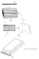
図1は半導体装置の収納容器がリールである場合の実施例を示した模式図で、乾燥剤1、リール2およびキャリアテープ7を脱気梱包用袋3に収容し密封する各過程と、梱包完了後の状態(斜視図および側面図)を示したものである。
FIG. 1 is a schematic view showing an embodiment in which the storage container of a semiconductor device is a reel. Each process of housing and sealing the
本実施例では、半導体装置が封入されたキャリアテープ7をリール巻き取り部に巻き取る際、キャリアテープ7をリール2の外周まで巻き取らずに、乾燥剤1が入るスペースを残しておく。そして、予め用意した短冊状(リールのフランジ間の寸法に相当する幅のもの)に包装された乾燥剤1をその残されたスペースに嵌合するように、円弧上に変形させて装着する。
In this embodiment, when the
乾燥剤を装着したリール2を脱気梱包用袋3に収容した後は、従来例と同じく脱気し、開口部を熱シールすることによって気密性のある半導体装置梱包体が得られる。なお、図1下左図の斜線部は熱シール部4である。出来上がった半導体装置梱包体は、梱包体側面図(図1下右図)が示すように上下面が平坦になっており、突起部はなく、保管、輸送に適した形状となっている。
After the
図2は半導体装置の収納容器がトレイである場合の実施例を示した模式図で、乾燥剤1と複数個のトレイ6を脱気梱包用袋3に収容し封入する各過程と、梱包完了後の状態(斜視図および側面図)を示したものである。
FIG. 2 is a schematic view showing an embodiment in which the storage container of the semiconductor device is a tray. Each process of storing and encapsulating the
本考案は、半導体装置の載置されたトレイ6と、その上に積層した(蓋部に相当する)別のトレイ6上の端部に乾燥剤1が載る凹部状のスペースを設けておき、このスペースに図示するような短冊状に包装された乾燥剤1を装着している。乾燥剤1の形状は、予めトレイの間隙に収まる幅で、必要な長さを有するものを用意しておけばよい。
The present invention provides a recessed space in which the
また、乾燥剤1を装着した上にさらに別の半導体装置の載置されたトレイ6を重ねる構造とすることもできる。即ち、トレイ6と別のトレイ6との間隙に乾燥剤1が載るスペースを設け、このスペースに短冊状の包装された乾燥剤1を装着する構造とすることもできる。
Further, a structure in which a
乾燥剤1を装着したトレイ6を脱気梱包用袋3に収容した後は、従来例と同じく脱気し、開口部を熱シールすることによって気密性のある半導体装置梱包体を形成することができる。なお、図の斜線部は熱シール部4である。出来上がった半導体装置梱包体は、図1の場合と同じく、梱包体の上下面が平坦になっており、保管、輸送に適した形状となっている。
After the
以上説明したように、半導体装置を収納する収納容器に、乾燥剤を装着するスペースを設けると共に、そのスペースに嵌合するように乾燥剤を装着することで、半導体装置や脱気梱包用袋の破損がなく、梱包サイズも小さい半導体装置梱包体を得ることができた。 As described above, a space for mounting the desiccant is provided in the storage container for storing the semiconductor device, and the desiccant is mounted so as to fit in the space, so that the semiconductor device and the deaeration packing bag It was possible to obtain a semiconductor device package having no damage and a small packing size.
1;乾燥剤、2;リール、3;脱気梱包用袋、4;熱シール部、5;突起部、
6;トレイ、7;キャリアテープ
DESCRIPTION OF
6; tray, 7; carrier tape
Claims (3)
前記収納容器内に前記乾燥剤を収納するスペースを備え、該スペースに嵌合する形状の乾燥剤が装着されていることを特徴とする半導体装置梱包体。 In the semiconductor device package body in which the desiccant is enclosed together with the storage container storing the semiconductor device inside the degassing packaging bag,
A package for a semiconductor device, comprising: a space for storing the desiccant in the storage container; and a desiccant having a shape that fits into the space.
前記収納容器が半導体装置を封入したキャリアテープを巻き取るリールであって、該リールの前記キャリアテープ巻き取り部に、巻き取られた前記キャリアテープに沿って、前記乾燥剤を収納する円弧状のスペースを備え、該スペースに嵌合する形状の前記乾燥剤が装着されていることを特徴とする半導体装置梱包体。 The semiconductor device package according to claim 1,
The storage container is a reel that winds up a carrier tape enclosing a semiconductor device, and the carrier tape winding portion of the reel has an arc shape that stores the desiccant along the wound carrier tape. A semiconductor device package comprising a space, and the desiccant having a shape fitting into the space.
前記収納容器が半導体装置を載置したトレイであって、該トレイと蓋部との間隙あるいは蓋部上に短冊状のスペースを設け、このスペースに嵌合する形状の前記乾燥剤が装着されていることを特徴とする半導体装置梱包体。
The semiconductor device package according to claim 1,
The storage container is a tray on which a semiconductor device is placed, and a gap between the tray and the lid or a strip-shaped space is provided on the lid, and the desiccant having a shape that fits into the space is mounted. A package for a semiconductor device.
Priority Applications (1)
| Application Number | Priority Date | Filing Date | Title |
|---|---|---|---|
| JP2005003397U JP3112546U (en) | 2005-05-19 | 2005-05-19 | Semiconductor device package |
Applications Claiming Priority (1)
| Application Number | Priority Date | Filing Date | Title |
|---|---|---|---|
| JP2005003397U JP3112546U (en) | 2005-05-19 | 2005-05-19 | Semiconductor device package |
Publications (1)
| Publication Number | Publication Date |
|---|---|
| JP3112546U true JP3112546U (en) | 2005-08-18 |
Family
ID=43274957
Family Applications (1)
| Application Number | Title | Priority Date | Filing Date |
|---|---|---|---|
| JP2005003397U Expired - Fee Related JP3112546U (en) | 2005-05-19 | 2005-05-19 | Semiconductor device package |
Country Status (1)
| Country | Link |
|---|---|
| JP (1) | JP3112546U (en) |
Cited By (1)
| Publication number | Priority date | Publication date | Assignee | Title |
|---|---|---|---|---|
| CN112996734A (en) * | 2018-11-14 | 2021-06-18 | 电化株式会社 | Package for containing heat radiation substrate and packing box |
-
2005
- 2005-05-19 JP JP2005003397U patent/JP3112546U/en not_active Expired - Fee Related
Cited By (2)
| Publication number | Priority date | Publication date | Assignee | Title |
|---|---|---|---|---|
| CN112996734A (en) * | 2018-11-14 | 2021-06-18 | 电化株式会社 | Package for containing heat radiation substrate and packing box |
| US11912489B2 (en) | 2018-11-14 | 2024-02-27 | Denka Company Limited | Package accommodating heat dissipation substrate and packing box |
Similar Documents
| Publication | Publication Date | Title |
|---|---|---|
| US7780004B2 (en) | Package for stick electrodes | |
| JP3046010B2 (en) | Storage container and storage method | |
| US8770840B2 (en) | Airbag structure with inner shade cover and manufacturing method thereof | |
| JP2007269391A (en) | Packaging unit and packaging method for glass substrate having electric conductive section formed therein | |
| JP3112546U (en) | Semiconductor device package | |
| JP2006290411A (en) | Semiconductor device storage body, packaging bag made of aluminum foil, and semiconductor device storage structure using it | |
| JP2001240138A (en) | Package and manufacturing method therefor | |
| JP2004269026A (en) | Packing method | |
| JP2008074451A (en) | Package and manufacturing method therefor | |
| JP2003034363A (en) | Packaging method | |
| JP2006306403A (en) | Manufacturing method of semiconductor device | |
| JPH0245368A (en) | Wrapping member for semiconductor device | |
| CN111252333A (en) | Single-flange packaging box and packaging method thereof | |
| KR200401579Y1 (en) | Package | |
| JP5542455B2 (en) | Packing equipment | |
| JP6068096B2 (en) | Package of wafer cassette | |
| JP2001055274A (en) | Packing container, semiconductor device, and manufacture of semiconductor device | |
| CN209906112U (en) | Cable shaft of unmanned submersible and packaging structure of unmanned submersible | |
| CN111319870A (en) | Carrier band for packaging electronic element and packaging method thereof | |
| JP2009298446A (en) | Storage container for optical device | |
| KR200227679Y1 (en) | Container with projection members for separation | |
| JPS61152576A (en) | Method of packaging lead frame | |
| JP6467702B2 (en) | Reel package | |
| JPH10250773A (en) | Moisture-proof packaging method and device | |
| CN114906486A (en) | Packaging material and method for manufacturing packaging material |
Legal Events
| Date | Code | Title | Description |
|---|---|---|---|
| R150 | Certificate of patent or registration of utility model |
Free format text: JAPANESE INTERMEDIATE CODE: R150 |
|
| FPAY | Renewal fee payment (event date is renewal date of database) |
Free format text: PAYMENT UNTIL: 20080706 Year of fee payment: 3 |
|
| FPAY | Renewal fee payment (event date is renewal date of database) |
Free format text: PAYMENT UNTIL: 20110706 Year of fee payment: 6 |
|
| FPAY | Renewal fee payment (event date is renewal date of database) |
Free format text: PAYMENT UNTIL: 20130706 Year of fee payment: 8 |
|
| R250 | Receipt of annual fees |
Free format text: JAPANESE INTERMEDIATE CODE: R250 |
|
| LAPS | Cancellation because of no payment of annual fees |