JP2025079110A - Method for producing circuit connection structure, adhesive film for circuit connection, and circuit connection structure - Google Patents
Method for producing circuit connection structure, adhesive film for circuit connection, and circuit connection structure Download PDFInfo
- Publication number
- JP2025079110A JP2025079110A JP2023191576A JP2023191576A JP2025079110A JP 2025079110 A JP2025079110 A JP 2025079110A JP 2023191576 A JP2023191576 A JP 2023191576A JP 2023191576 A JP2023191576 A JP 2023191576A JP 2025079110 A JP2025079110 A JP 2025079110A
- Authority
- JP
- Japan
- Prior art keywords
- circuit connection
- adhesive layer
- component
- circuit
- adhesive film
- Prior art date
- Legal status (The legal status is an assumption and is not a legal conclusion. Google has not performed a legal analysis and makes no representation as to the accuracy of the status listed.)
- Pending
Links
Images


Classifications
-
- C—CHEMISTRY; METALLURGY
- C09—DYES; PAINTS; POLISHES; NATURAL RESINS; ADHESIVES; COMPOSITIONS NOT OTHERWISE PROVIDED FOR; APPLICATIONS OF MATERIALS NOT OTHERWISE PROVIDED FOR
- C09J—ADHESIVES; NON-MECHANICAL ASPECTS OF ADHESIVE PROCESSES IN GENERAL; ADHESIVE PROCESSES NOT PROVIDED FOR ELSEWHERE; USE OF MATERIALS AS ADHESIVES
- C09J11/00—Features of adhesives not provided for in group C09J9/00, e.g. additives
- C09J11/02—Non-macromolecular additives
- C09J11/04—Non-macromolecular additives inorganic
-
- C—CHEMISTRY; METALLURGY
- C09—DYES; PAINTS; POLISHES; NATURAL RESINS; ADHESIVES; COMPOSITIONS NOT OTHERWISE PROVIDED FOR; APPLICATIONS OF MATERIALS NOT OTHERWISE PROVIDED FOR
- C09J—ADHESIVES; NON-MECHANICAL ASPECTS OF ADHESIVE PROCESSES IN GENERAL; ADHESIVE PROCESSES NOT PROVIDED FOR ELSEWHERE; USE OF MATERIALS AS ADHESIVES
- C09J163/00—Adhesives based on epoxy resins; Adhesives based on derivatives of epoxy resins
-
- C—CHEMISTRY; METALLURGY
- C09—DYES; PAINTS; POLISHES; NATURAL RESINS; ADHESIVES; COMPOSITIONS NOT OTHERWISE PROVIDED FOR; APPLICATIONS OF MATERIALS NOT OTHERWISE PROVIDED FOR
- C09J—ADHESIVES; NON-MECHANICAL ASPECTS OF ADHESIVE PROCESSES IN GENERAL; ADHESIVE PROCESSES NOT PROVIDED FOR ELSEWHERE; USE OF MATERIALS AS ADHESIVES
- C09J7/00—Adhesives in the form of films or foils
- C09J7/30—Adhesives in the form of films or foils characterised by the adhesive composition
- C09J7/35—Heat-activated
-
- C—CHEMISTRY; METALLURGY
- C09—DYES; PAINTS; POLISHES; NATURAL RESINS; ADHESIVES; COMPOSITIONS NOT OTHERWISE PROVIDED FOR; APPLICATIONS OF MATERIALS NOT OTHERWISE PROVIDED FOR
- C09J—ADHESIVES; NON-MECHANICAL ASPECTS OF ADHESIVE PROCESSES IN GENERAL; ADHESIVE PROCESSES NOT PROVIDED FOR ELSEWHERE; USE OF MATERIALS AS ADHESIVES
- C09J9/00—Adhesives characterised by their physical nature or the effects produced, e.g. glue sticks
- C09J9/02—Electrically-conducting adhesives
-
- H—ELECTRICITY
- H01—ELECTRIC ELEMENTS
- H01R—ELECTRICALLY-CONDUCTIVE CONNECTIONS; STRUCTURAL ASSOCIATIONS OF A PLURALITY OF MUTUALLY-INSULATED ELECTRICAL CONNECTING ELEMENTS; COUPLING DEVICES; CURRENT COLLECTORS
- H01R11/00—Individual connecting elements providing two or more spaced connecting locations for conductive members which are, or may be, thereby interconnected, e.g. end pieces for wires or cables supported by the wire or cable and having means for facilitating electrical connection to some other wire, terminal, or conductive member, blocks of binding posts
- H01R11/01—Individual connecting elements providing two or more spaced connecting locations for conductive members which are, or may be, thereby interconnected, e.g. end pieces for wires or cables supported by the wire or cable and having means for facilitating electrical connection to some other wire, terminal, or conductive member, blocks of binding posts characterised by the form or arrangement of the conductive interconnection between the connecting locations
-
- H—ELECTRICITY
- H05—ELECTRIC TECHNIQUES NOT OTHERWISE PROVIDED FOR
- H05K—PRINTED CIRCUITS; CASINGS OR CONSTRUCTIONAL DETAILS OF ELECTRIC APPARATUS; MANUFACTURE OF ASSEMBLAGES OF ELECTRICAL COMPONENTS
- H05K1/00—Printed circuits
- H05K1/02—Details
- H05K1/14—Structural association of two or more printed circuits
-
- H—ELECTRICITY
- H05—ELECTRIC TECHNIQUES NOT OTHERWISE PROVIDED FOR
- H05K—PRINTED CIRCUITS; CASINGS OR CONSTRUCTIONAL DETAILS OF ELECTRIC APPARATUS; MANUFACTURE OF ASSEMBLAGES OF ELECTRICAL COMPONENTS
- H05K3/00—Apparatus or processes for manufacturing printed circuits
- H05K3/30—Assembling printed circuits with electric components, e.g. with resistors
- H05K3/32—Assembling printed circuits with electric components, e.g. with resistors electrically connecting electric components or wires to printed circuits
-
- H—ELECTRICITY
- H05—ELECTRIC TECHNIQUES NOT OTHERWISE PROVIDED FOR
- H05K—PRINTED CIRCUITS; CASINGS OR CONSTRUCTIONAL DETAILS OF ELECTRIC APPARATUS; MANUFACTURE OF ASSEMBLAGES OF ELECTRICAL COMPONENTS
- H05K3/00—Apparatus or processes for manufacturing printed circuits
- H05K3/36—Assembling printed circuits with other printed circuits
Landscapes
- Engineering & Computer Science (AREA)
- Chemical & Material Sciences (AREA)
- Organic Chemistry (AREA)
- Microelectronics & Electronic Packaging (AREA)
- Manufacturing & Machinery (AREA)
- Inorganic Chemistry (AREA)
- Adhesives Or Adhesive Processes (AREA)
- Adhesive Tapes (AREA)
- Combinations Of Printed Boards (AREA)
Abstract
Description
本開示は、回路接続構造体の製造方法、回路接続用接着剤フィルム、及び回路接続構造体に関する。 The present disclosure relates to a method for manufacturing a circuit connection structure, an adhesive film for circuit connection, and a circuit connection structure.
従来、テレビ、PCモニタ、携帯電話、スマートホン等の各種表示手段として、液晶表示パネル、有機ELパネル等が用いられている。このような表示装置においては、ファインピッチ化、軽量薄型化等の観点から、駆動用ICを直接表示パネルのガラス基板上に実装するいわゆるCOG(chip on glass)実装が採用されている。 Conventionally, liquid crystal display panels, organic EL panels, etc. have been used as various display means for televisions, PC monitors, mobile phones, smartphones, etc. In such display devices, from the viewpoints of fine pitch, light weight and thinness, so-called COG (chip on glass) mounting is adopted in which a driving IC is mounted directly on the glass substrate of the display panel.
COG実装方式が採用された液晶表示パネルにおいては、例えば、透明電極(ITO(酸化インジウムスズ)等)を複数有する透明基板(ガラス基板等)上に、液晶駆動用IC等の半導体素子が接続される。半導体素子の電極端子と透明電極との接続のための接着材料として、接着剤中に導電粒子が分散された異方導電性を有する回路接続用接着剤フィルムが使用されている。例えば、半導体素子として液晶駆動用ICを実装する場合、液晶駆動用ICは、その実装面に透明電極に対応した複数の電極端子を有しており、異方導電性を有する回路接続用接着剤フィルムを介して液晶駆動用ICを透明基板上に熱圧着することによって、電極端子と透明電極とが接続されて、回路接続構造体を得ることができる。 In a liquid crystal display panel that employs the COG mounting method, for example, a semiconductor element such as a liquid crystal driving IC is connected to a transparent substrate (such as a glass substrate) having a plurality of transparent electrodes (such as ITO (indium tin oxide)). An adhesive film for circuit connection having anisotropic conductivity in which conductive particles are dispersed in the adhesive is used as an adhesive material for connecting the electrode terminals of the semiconductor element to the transparent electrodes. For example, when mounting a liquid crystal driving IC as a semiconductor element, the liquid crystal driving IC has a plurality of electrode terminals corresponding to the transparent electrodes on its mounting surface, and the electrode terminals and the transparent electrodes are connected by thermocompression bonding the liquid crystal driving IC onto the transparent substrate via the circuit connection adhesive film having anisotropic conductivity, thereby obtaining a circuit connection structure.
近年、POELD(Plasitic Organic Electro-Luminescence Diode:有機発光ダイオード)ディスプレイなどの曲面を有するディスプレイ(フレキシブルディスプレイ)が提案されている。このようなフレキシブルディスプレイでは、基板としてガラス基板に替えて可撓性を有するプラスチック基板(ポリイミド基板等)が用いられるため、駆動用IC等の各種電子部品もプラスチック基板に実装されることとなる。そのような実装の方法として、異方導電性を有する回路接続用接着剤フィルムを用いるCOP(chip on plastic)実装が検討されている(例えば、特許文献1参照)。 In recent years, displays with curved surfaces (flexible displays), such as POELD (Plastic Organic Electro-Luminescence Diode) displays, have been proposed. In such flexible displays, flexible plastic substrates (polyimide substrates, etc.) are used instead of glass substrates, and various electronic components such as driving ICs are also mounted on the plastic substrates. As a method of such mounting, COP (chip on plastic) mounting using an anisotropically conductive circuit connection adhesive film is being considered (see, for example, Patent Document 1).
電流駆動であるOELDにおいては対向する電極間の接続抵抗をより低減することが求められている。一方で、異方導電性を有する回路接続用接着剤フィルムを用いて実装する場合には、短時間の実装条件で充分な接着強度を発現できることも要求される。 In current-driven OELDs, there is a demand for further reduction in the connection resistance between opposing electrodes. On the other hand, when mounting using an adhesive film for circuit connection with anisotropic conductivity, there is also a demand for sufficient adhesive strength to be achieved under short mounting conditions.
回路接続構造体の接続抵抗を低減する手法としては、電極と導電粒子との接触を良好にする目的で、導電粒子の粒子硬度の調整や接着剤フィルムの最低溶融粘度を低くすることなどが知られている。しかしながら、これらの手法のみでは、短時間実装によって、信頼性試験後においても接続抵抗値が上昇にしにくい回路接続構造体を得ることは難しい。 Known methods for reducing the connection resistance of a circuit connection structure include adjusting the particle hardness of the conductive particles and lowering the minimum melt viscosity of the adhesive film in order to improve contact between the electrodes and the conductive particles. However, using these methods alone, it is difficult to obtain a circuit connection structure in which the connection resistance value is unlikely to increase even after reliability testing through short-time mounting.
そこで、本開示は、対向電極間の接続抵抗値の低減を図りつつ、充分な接着強度で接続され、優れた接続信頼性を有する回路接続構造体を得ることを可能とする回路接続構造体の製造方法及び回路接続用接着剤フィルムを提供することを主な目的とする。 Therefore, the main objective of the present disclosure is to provide a method for producing a circuit connection structure and an adhesive film for circuit connection that can reduce the connection resistance between opposing electrodes while providing a circuit connection structure that is connected with sufficient adhesive strength and has excellent connection reliability.
本開示の一側面は、下記の[1]~[12]に関する。 One aspect of the present disclosure relates to the following [1] to [12].
[1] 第1の電極を有する第1の回路部材と、第2の電極を有する第2の回路部材との間に、導電粒子を含有する回路接続用接着剤フィルムを介在させ、前記第1の回路部材及び前記第2の回路部材を熱圧着して、前記第1の電極及び前記第2の電極を互いに電気的に接続する工程を備え、前記回路接続用接着剤フィルムが、導電粒子及び第1の熱硬化性樹脂成分を含有する第1の接着剤層と、前記第1の接着剤層上に設けられた、第2の熱硬化性樹脂成分を含有する第2の接着剤層と、を有し、前記回路接続用接着剤フィルムは、示差走査熱量曲線から得られる反応開始温度T1と反応ピーク温度Tmaxとの差(Tmax-T1)が20℃以下である、回路接続構造体の製造方法。
[2] 前記反応開始温度T1が、100~110℃である、[1]に記載の回路接続構造体の製造方法。
[3] 前記第1の回路部材及び前記第2の回路部材を熱圧着するときの接続温度が、170~220℃であり、加熱開始時から1秒後に前記接続温度の80%以上の温度となるように前記第1の回路部材及び前記第2の回路部材を熱圧着する、[1]又は[2]に記載の回路接続構造体の製造方法。
[4] 前記第1の熱硬化性樹脂成分及び前記第2の熱硬化性樹脂成分が、カチオン重合性化合物及び熱カチオン重合開始剤を含み、前記第1の接着剤層が光硬化性樹脂成分の硬化物を更に含有し、前記光硬化性樹脂成分がラジカル重合性化合物及び光ラジカル重合開始剤を含む、[1]~[3]のいずれかに記載の回路接続構造体の製造方法。
[5] 前記カチオン重合性化合物が、オキセタン化合物及び脂環式エポキシ化合物からなる群より選ばれる少なくとも1種の化合物である、[4]に記載の回路接続構造体の製造方法。
[6] 前記第1の接着剤層の厚さが5.0μm以下である、[1]~[5]のいずれかに記載の回路接続構造体の製造方法。
[7] 導電粒子及び第1の熱硬化性樹脂成分を含有する第1の接着剤層と、前記第1の接着剤層上に設けられた、第2の熱硬化性樹脂成分を含有する第2の接着剤層と、を有し、示差走査熱量曲線から得られる反応開始温度T1と反応ピーク温度Tmaxとの差(Tmax-T1)が20℃以下である、回路接続用接着剤フィルム。
[8] 前記反応開始温度T1が、100~110℃である、[7]に記載の回路接続用接着剤フィルム。
[9] 前記第1の熱硬化性樹脂成分及び前記第2の熱硬化性樹脂成分が、カチオン重合性化合物及び熱カチオン重合開始剤を含み、前記第1の接着剤層が光硬化性樹脂成分の硬化物を更に含有し、前記光硬化性樹脂成分がラジカル重合性化合物及び光ラジカル重合開始剤を含む、「7」又は[8]に記載の回路接続用接着剤フィルム。
[10] 前記カチオン重合性化合物が、オキセタン化合物及び脂環式エポキシ化合物からなる群より選ばれる少なくとも1種の化合物である、[9]に記載の回路接続用接着剤フィルム。
[11] 前記第1の接着剤層の厚さが5.0μm以下である、[7]~[10]のいずれかに記載の回路接続用接着剤フィルム。
[12] 第1の電極を有する第1の回路部材と、第2の電極を有する第2の回路部材と、前記第1の回路部材及び前記第2の回路部材の間に配置され、前記第1の電極及び前記第2の電極を互いに電気的に接続する回路接続部と、を備え、前記回路接続部が、[7]~[11]のいずれか一項に記載の回路接続用接着剤フィルムの硬化体を含む、回路接続構造体。
[1] A method for producing a circuit connection structure, comprising the steps of: interposing an adhesive film for circuit connection containing conductive particles between a first circuit member having a first electrode and a second circuit member having a second electrode; and thermocompression bonding the first circuit member and the second circuit member to electrically connect the first electrode and the second electrode to each other; the adhesive film for circuit connection has a first adhesive layer containing conductive particles and a first thermosetting resin component, and a second adhesive layer containing a second thermosetting resin component provided on the first adhesive layer; and the adhesive film for circuit connection has a difference (Tmax-T1) between a reaction start temperature T1 and a reaction peak temperature Tmax obtained from a differential scanning calorimetry curve of 20°C or less.
[2] The method for producing a circuit connection structure according to [1], wherein the reaction initiation temperature T1 is 100 to 110° C.
[3] The method for producing a circuit connection structure according to [1] or [2], wherein the connection temperature when the first circuit member and the second circuit member are thermocompression-bonded is 170 to 220°C, and the first circuit member and the second circuit member are thermocompression-bonded so that the temperature becomes 80% or more of the
[4] The method for producing a circuit connection structure according to any one of [1] to [3], wherein the first thermosetting resin component and the second thermosetting resin component contain a cationic polymerizable compound and a thermal cationic polymerization initiator, the first adhesive layer further contains a cured product of a photocurable resin component, and the photocurable resin component contains a radical polymerizable compound and a photoradical polymerization initiator.
[5] The method for producing a circuit connection structure according to [4], wherein the cationically polymerizable compound is at least one compound selected from the group consisting of an oxetane compound and an alicyclic epoxy compound.
[6] The method for producing a circuit connection structure according to any one of [1] to [5], wherein the first adhesive layer has a thickness of 5.0 μm or less.
[7] An adhesive film for circuit connection, comprising a first adhesive layer containing conductive particles and a first thermosetting resin component, and a second adhesive layer provided on the first adhesive layer and containing a second thermosetting resin component, wherein the difference (Tmax-T1) between the reaction start temperature T1 and the reaction peak temperature Tmax obtained from a differential scanning calorimetry curve is 20°C or less.
[8] The adhesive film for circuit connection according to [7], wherein the reaction initiation temperature T1 is 100 to 110° C.
[9] The adhesive film for circuit connection described in [7] or [8], wherein the first thermosetting resin component and the second thermosetting resin component contain a cationic polymerizable compound and a thermal cationic polymerization initiator, the first adhesive layer further contains a cured product of a photocurable resin component, and the photocurable resin component contains a radical polymerizable compound and a photoradical polymerization initiator.
[10] The adhesive film for circuit connection according to [9], wherein the cationically polymerizable compound is at least one compound selected from the group consisting of oxetane compounds and alicyclic epoxy compounds.
[11] The adhesive film for circuit connection according to any one of [7] to [10], wherein the first adhesive layer has a thickness of 5.0 μm or less.
[12] A circuit connection structure comprising: a first circuit member having a first electrode; a second circuit member having a second electrode; and a circuit connection portion disposed between the first circuit member and the second circuit member and electrically connecting the first electrode and the second electrode to each other, wherein the circuit connection portion comprises a cured product of the adhesive film for circuit connection according to any one of [7] to [11].
上記[1]に記載の回路接続構造体の製造方法によれば、対向電極間の接続抵抗値の低減を図りつつ、充分な接着強度で接続され、優れた接続信頼性を有する回路接続構造体を得ることができる。このような効果が奏される理由については、Tmax-T1が20℃以下である、すなわち反応開始温度を高めた回路接続用接着剤フィルムを用いることにより、樹脂の排除性が向上して接続ギャップ(接続された対向する電極間の距離)が小さくなり、これにより導電粒子と電極との接触面積を大きくすることができたためと考えられる。 According to the manufacturing method of the circuit connection structure described in [1] above, it is possible to obtain a circuit connection structure that is connected with sufficient adhesive strength and has excellent connection reliability while reducing the connection resistance value between opposing electrodes. The reason for this effect is thought to be that by using a circuit connection adhesive film with Tmax-T1 of 20°C or less, i.e., with an increased reaction start temperature, the resin removal is improved and the connection gap (the distance between the connected opposing electrodes) is reduced, thereby making it possible to increase the contact area between the conductive particles and the electrodes.
本開示によれば、対向電極間の接続抵抗値の低減を図りつつ、充分な接着強度で接続され、優れた接続信頼性を有する回路接続構造体を得ることを可能とする回路接続構造体の製造方法及び回路接続用接着剤フィルムを提供することができる。上記で得られる回路接続構造体は、高温高湿環境下での信頼性試験後であっても対向電極間の接続抵抗値が上昇しにくいものになり得る。 According to the present disclosure, it is possible to provide a manufacturing method for a circuit connection structure and an adhesive film for circuit connection that can obtain a circuit connection structure that is connected with sufficient adhesive strength and has excellent connection reliability while reducing the connection resistance value between opposing electrodes. The circuit connection structure obtained as described above can be one in which the connection resistance value between opposing electrodes is unlikely to increase even after a reliability test in a high-temperature, high-humidity environment.
ところで、近年のディスプレイの高画素化に伴い、ドライバICの電極小面積化、狭ピッチ化が進んでいる。このような場合、導電粒子の捕捉率を高めながら隣り合う電極間の絶縁性能を確保することが難しくなる。これに対し、本開示の回路接続構造体の製造方法及び回路接続用接着剤フィルムによれば、上述した接続ギャップを小さくすることで対向電極間の接続抵抗値の低減を図ることができることから、電極小面積化及び狭ピッチ化へも充分対応することが可能である。 However, in recent years, with displays becoming more pixelated, the electrodes of driver ICs are becoming smaller in area and narrower in pitch. In such cases, it becomes difficult to ensure the insulation performance between adjacent electrodes while increasing the capture rate of conductive particles. In contrast, with the manufacturing method of the circuit connection structure and the adhesive film for circuit connection disclosed herein, the connection gap described above can be reduced to reduce the connection resistance between opposing electrodes, making it possible to fully respond to the trend toward smaller electrode area and narrower pitch.
以下、図面を参照しながら本開示の実施形態について詳細に説明する。以下の説明では、同一又は相当部分には同一符号を付し、重複する説明は省略する。なお、本開示は以下の実施形態に限定されるものではない。 The following describes in detail the embodiments of the present disclosure with reference to the drawings. In the following description, the same or equivalent parts are given the same reference numerals, and duplicate descriptions are omitted. Note that the present disclosure is not limited to the following embodiments.
本明細書中、「~」を用いて示された数値範囲は、「~」の前後に記載される数値をそれぞれ最小値及び最大値として含む範囲を示す。本明細書中に段階的に記載されている数値範囲において、ある段階の数値範囲の上限値又は下限値は、他の段階の数値範囲の上限値又は下限値に置き換えてもよい。また、本明細書中に記載されている数値範囲において、その数値範囲の上限値又は下限値は、実施例に示されている値に置き換えてもよい。また、個別に記載した上限値及び下限値は任意に組み合わせ可能である。数値範囲「A~B」という表記においては、両端の数値A及びBがそれぞれ下限値及び上限値として数値範囲に含まれる。本明細書において、例えば、「10以上」という記載は、「10」と「10を超える数値」とを意味し、数値が異なる場合もこれに準ずる。また、例えば、「10以下」という記載は、「10」と「10未満の数値」とを意味し、数値が異なる場合もこれに準ずる。また、本明細書において、「(メタ)アクリレート」とは、アクリレート、及び、それに対応するメタクリレートの少なくとも一方を意味する。「(メタ)アクリロイル」、「(メタ)アクリル酸」等の他の類似の表現においても同様である。また、「A又はB」とは、A及びBのどちらか一方を含んでいればよく、両方とも含んでいてもよい。また、以下で例示する材料は、特に断らない限り、1種単独で用いてもよく、2種以上を組み合わせて用いてもよい。組成物中の各成分の含有量は、組成物中に各成分に該当する物質が複数存在する場合、特に断らない限り、組成物中に存在する当該複数の物質の合計量を意味する。 In this specification, the numerical range indicated by "~" indicates a range including the numerical values before and after "~" as the minimum and maximum values, respectively. In the numerical ranges described in stages in this specification, the upper or lower limit of a certain numerical range may be replaced with the upper or lower limit of the numerical range of another stage. In addition, in the numerical ranges described in this specification, the upper or lower limit of the numerical range may be replaced with the value shown in the examples. In addition, the upper and lower limits described individually can be arbitrarily combined. In the expression of a numerical range "A~B", the numerical values A and B at both ends are included in the numerical range as the lower and upper limits, respectively. In this specification, for example, the description "10 or more" means "10" and "a numerical value exceeding 10", and this also applies when the numerical values are different. In addition, for example, the description "10 or less" means "10" and "a numerical value less than 10", and this also applies when the numerical values are different. In addition, in this specification, "(meth)acrylate" means at least one of acrylate and the corresponding methacrylate. The same applies to other similar expressions such as "(meth)acryloyl" and "(meth)acrylic acid". Furthermore, "A or B" means that either A or B is included, and both may be included. Furthermore, unless otherwise specified, the materials exemplified below may be used alone or in combination of two or more. When multiple substances corresponding to each component are present in the composition, the content of each component in the composition means the total amount of the multiple substances present in the composition, unless otherwise specified.
[回路接続用接着剤フィルム]
本実施形態の回路接続用接着剤フィルムは、導電粒子及び第1の熱硬化性樹脂成分を含有する第1の接着剤層と、第1の接着剤層上に設けられた、第2の熱硬化性樹脂成分を含有する第2の接着剤層とを備える。第1の接着剤層は、光硬化性樹脂成分を更に含有していてもよい。光硬化性樹脂成分は、ラジカル重合性化合物及び光ラジカル重合開始剤を含むことができる。
[Adhesive film for circuit connection]
The adhesive film for circuit connection of this embodiment includes a first adhesive layer containing conductive particles and a first thermosetting resin component, and a second adhesive layer provided on the first adhesive layer and containing a second thermosetting resin component. The first adhesive layer may further contain a photocurable resin component. The photocurable resin component may include a radical polymerizable compound and a photoradical polymerization initiator.
本実施形態の回路接続用接着剤フィルムは、示差走査熱量曲線から得られる反応開始温度T1と反応ピーク温度Tmaxとの差(Tmax-T1)が20℃以下である。 The circuit connection adhesive film of this embodiment has a difference (Tmax-T1) between the reaction start temperature T1 and the reaction peak temperature Tmax obtained from the differential scanning calorimetry curve of 20°C or less.
接着剤フィルムの示差走査熱量曲線は、接着剤フィルムを10mg秤量し、示差走査熱量分析(DSC)装置を使用し、窒素雰囲気下、昇温速度10℃/分、測定温度範囲0~300℃で測定することにより得ることができる。反応開始温度T1は、物質(接着剤フィルム)に熱を与えた際に、物質(接着剤フィルム)の発熱の開始点として定義される温度である。反応ピーク温度Tmaxは、物質(接着剤フィルム)の発熱量が最大となる点として定義される温度である。 The differential scanning calorimetry curve of the adhesive film can be obtained by weighing out 10 mg of the adhesive film and measuring using a differential scanning calorimetry (DSC) analyzer in a nitrogen atmosphere at a heating rate of 10°C/min and a measurement temperature range of 0 to 300°C. The reaction start temperature T1 is the temperature defined as the temperature at which the substance (adhesive film) starts to generate heat when heat is applied to the substance (adhesive film). The reaction peak temperature Tmax is the temperature defined as the point at which the amount of heat generated by the substance (adhesive film) is maximum.
(Tmax-T1)を20℃以下にする方法としては、第1の熱硬化性樹脂成分及び第2の熱硬化性樹脂成分がカチオン重合系である場合はカチオン安定化剤を併用すること、重合速度の速いカチオン重合性化合物を使用すること等が挙げられる。 Methods for keeping (Tmax-T1) at 20°C or less include using a cationic stabilizer in combination when the first thermosetting resin component and the second thermosetting resin component are cationic polymerization systems, and using a cationic polymerizable compound with a high polymerization rate.
(Tmax-T1)は、接続ギャップを小さくする観点から、14~20℃であってもよく、14~17℃であってもよい。 From the viewpoint of reducing the connection gap, (Tmax-T1) may be 14 to 20°C, or 14 to 17°C.
反応開始温度T1は、接続ギャップを小さくする観点から、100~110℃であってもよく、100~106℃であってもよい。反応開始温度T1は、例えば、第1の熱硬化性樹脂成分及び第2の熱硬化性樹脂成分がカチオン重合系である場合、熱カチオン開始剤の含有量、カチオン重合性化合物の含有量及び種類によって調整することができる。 From the viewpoint of reducing the connection gap, the reaction initiation temperature T1 may be 100 to 110°C or 100 to 106°C. For example, when the first thermosetting resin component and the second thermosetting resin component are cationic polymerization systems, the reaction initiation temperature T1 can be adjusted by the content of the thermal cationic initiator and the content and type of the cationic polymerizable compound.
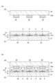
図1は、回路接続用接着剤フィルムの一実施形態を示す模式断面図であり、回路接続用接着剤フィルムの縦断面を模式的に示す図である。図1に示される回路接続用接着剤フィルム10は、複数の導電粒子4及び接着剤成分3を含有する第1の接着剤層1と、第1の接着剤層1上に設けられた第2の接着剤層2とを備える。本明細書において、「縦断面」とは、主面(例えば、回路接続用接着剤フィルム10)に対して直交する断面(厚さ方向の断面)を意味する。
Figure 1 is a schematic cross-sectional view showing one embodiment of an adhesive film for circuit connection, and is a diagram showing a schematic longitudinal section of the adhesive film for circuit connection. The adhesive film for
複数の導電粒子4の少なくとも一部は、回路接続用接着剤フィルム10の縦断面において、隣り合う導電粒子同士が互いに離隔した状態で横方向に並んでいてもよい。ここで、「横方向」とは、回路接続用接着剤フィルムの主面と平行な方向(図1における左右方向)を意味する。なお、図1では、導電粒子4の一部が第1の接着剤層1の表面から露出(例えば、第2の接着剤層2側に突出)しているが、導電粒子4が第1の接着剤層1の表面から露出しないように、導電粒子4の全体が第1の接着剤層1中に埋め込まれていてもよい(導電粒子4が第1の接着剤層1中に分散されていてもよい)。
At least some of the
回路接続用接着剤フィルム10は、異方導電性を有する回路接続用接着剤フィルム(異方導電性接着剤フィルム)であり、第1の電極を有する第1の回路部材と、第2の電極を有する第2の回路部材との間に介在させ、第1の回路部材及び第2の回路部材を熱圧着して、第1の電極及び第2の電極を互いに電気的に接続するために用いられるものであってよい。なお、「異方導電性」とは、加圧方向には導通し、非加圧方向では絶縁性を保つことを意味する。
The circuit connection
次に、第1の接着剤層1及び第2の接着剤層2を構成する各成分について説明する。
Next, we will explain the components that make up the first
<第1の接着剤層>
第1の接着剤層1は、例えば、導電粒子4(以下、「(A)成分」という場合がある。)、光硬化性樹脂成分(以下、「(B)成分」という場合がある。)の硬化物、及び熱硬化性樹脂成分(以下、「(C)成分」という場合がある。)を含有することができる。(B)成分の硬化物は、(B)成分を完全に硬化させた硬化物であってもよく、(B)成分の一部を硬化させた硬化物であってもよい。(C)成分は、接続時に流動可能な成分であり、例えば、未硬化の硬化性成分(例えば、樹脂成分)である。第1の接着剤層1を構成する導電粒子4以外の成分は、例えば、導電性を有しない成分(例えば、絶縁性樹脂成分)である。
<First Adhesive Layer>
The first
[(A)成分:導電粒子]
(A)成分は、導電性を有する粒子であれば特に制限されず、Au、Ag、Pd、Ni、Cu、はんだ等の金属で構成された金属粒子、導電性カーボンで構成された導電性カーボン粒子などであってよい。(A)成分は、非導電性のガラス、セラミック、プラスチック(ポリスチレン等)などを含む核と、上記金属又は上記導電性カーボンを含み、核を被覆する被覆層とを備える被覆導電粒子であってもよい。(A)成分は、各種導電粒子の1種を単独で用いてもよく、複数を組み合わせて用いてもよい。これらの中でも、(A)成分は、好ましくは、プラスチックを含む核と、金属若しくは導電性カーボンを含み、核を被覆する被覆層とを備える被覆導電粒子である。
[Component (A): Conductive particles]
The (A) component is not particularly limited as long as it is a particle having electrical conductivity, and may be a metal particle composed of a metal such as Au, Ag, Pd, Ni, Cu, or solder, or a conductive carbon particle composed of conductive carbon. The (A) component may be a coated conductive particle having a core containing non-conductive glass, ceramic, plastic (polystyrene, etc.), and a coating layer containing the above metal or the above conductive carbon and coating the core. The (A) component may be one of various conductive particles used alone, or a combination of multiple conductive particles. Among these, the (A) component is preferably a coated conductive particle having a core containing plastic and a coating layer containing a metal or conductive carbon and coating the core.
(A)成分が被覆導電粒子である場合、熱硬化性樹脂成分の硬化物を加熱又は加圧により変形させることが容易となるため、電極同士を電気的に接続する際に、電極と(A)成分との接触面積を増加させ、電極間の導電性をより向上させることができる。 When component (A) is a coated conductive particle, the cured product of the thermosetting resin component can be easily deformed by heating or applying pressure, so that when the electrodes are electrically connected to each other, the contact area between the electrodes and component (A) can be increased, and the conductivity between the electrodes can be further improved.
(A)成分の粒子硬度は、接続ギャップを小さくする観点から、1,000~30,000N/mm2であってもよく、3,000~200,000N/mm2であってもよい。なお、粒子硬度とは、微小圧縮試験機(プローブ先端形状:50μm×50μmの正方形)を用いて測定温度25℃で測定される値である。 From the viewpoint of reducing the connection gap, the particle hardness of the (A) component may be 1,000 to 30,000 N/ mm2 , or may be 3,000 to 200,000 N/ mm2 . The particle hardness is a value measured at a measurement temperature of 25°C using a microcompression tester (probe tip shape: 50 μm × 50 μm square).
(A)成分の粒子硬度は、1,000~9,000N/mm2であってもよく、3,000~9,000N/mm2であってもよい。この場合、高温高湿環境下であっても、回路接続構造体の対向電極間の接続抵抗値が上昇しにくくなる。また、(A)成分の粒子硬度は、回路接続構造体の対向電極間の接続抵抗値を低減する観点から、10,000~200,000N/mm2であってもよく、10,000~30,0000N/mm2であってもよい。 The particle hardness of component (A) may be 1,000 to 9,000 N/ mm2 , or may be 3,000 to 9,000 N/ mm2 . In this case, even in a high-temperature and high-humidity environment, the connection resistance between the opposing electrodes of the circuit connection structure is less likely to increase. In addition, from the viewpoint of reducing the connection resistance between the opposing electrodes of the circuit connection structure, the particle hardness of component (A) may be 10,000 to 200,000 N/ mm2 , or may be 10,000 to 30,0000 N/ mm2 .
(A)成分の最大粒径は、電極の最小間隔(隣り合う電極間の最短距離)よりも小さいことが必要である。(A)成分の最大粒径は、分散性及び導電性に優れる観点から、1.0μm以上、2.0μm以上、又は2.5μm以上であってよい。(A)成分の最大粒径は、分散性及び導電性に優れる観点から、30.0μm以下、25.0μm以下、20.0μm以下、15.0μm以下、10.0μm以下、又は5.0μm以下であってよい。本明細書では、第1の接着剤層中の任意の(A)成分300個(pcs)について、走査型電子顕微鏡(SEM)を用いた観察により粒径を測定し、得られた最も大きい値を(A)成分の最大粒径とする。なお、(A)成分が突起を有する場合等、(A)成分が球形ではない場合、(A)成分の粒径は、SEMの画像における導電粒子に外接する円の直径とする。 The maximum particle size of the (A) component must be smaller than the minimum distance between the electrodes (the shortest distance between adjacent electrodes). The maximum particle size of the (A) component may be 1.0 μm or more, 2.0 μm or more, or 2.5 μm or more, from the viewpoint of excellent dispersibility and conductivity. The maximum particle size of the (A) component may be 30.0 μm or less, 25.0 μm or less, 20.0 μm or less, 15.0 μm or less, 10.0 μm or less, or 5.0 μm or less, from the viewpoint of excellent dispersibility and conductivity. In this specification, the particle size of any 300 (pcs) of the (A) component in the first adhesive layer is measured by observation using a scanning electron microscope (SEM), and the largest value obtained is defined as the maximum particle size of the (A) component. Note that when the (A) component has protrusions or the like and is not spherical, the particle size of the (A) component is defined as the diameter of a circle circumscribing the conductive particle in the SEM image.
(A)成分の平均粒径は、分散性及び導電性に優れる観点から、1.0μm以上、2.0μm以上、2.5μm以上、又は3.0μm以上であってよい。(A)成分の平均粒径は、分散性及び導電性に優れる観点から、20.0μm以下、10.0μm以下、7.0μm以下、又は5.0μm以下であってよい。本明細書では、第1の接着剤層中の任意の(A)成分300個(pcs)について、走査型電子顕微鏡(SEM)を用いた観察により粒径を測定し、得られた粒径の平均値を平均粒径とする。 The average particle size of the (A) component may be 1.0 μm or more, 2.0 μm or more, 2.5 μm or more, or 3.0 μm or more, from the viewpoint of excellent dispersibility and conductivity. The average particle size of the (A) component may be 20.0 μm or less, 10.0 μm or less, 7.0 μm or less, or 5.0 μm or less, from the viewpoint of excellent dispersibility and conductivity. In this specification, the particle size of any 300 pieces (pcs) of the (A) component in the first adhesive layer is measured by observation using a scanning electron microscope (SEM), and the average value of the obtained particle sizes is defined as the average particle size.
第1の接着剤層1において、(A)成分は均一に分散されていることが好ましい。回路接続用接着剤フィルム10における(A)成分の粒子密度は、安定した接続抵抗が得られる観点から、100個/mm2以上、1000個/mm2以上、3000個/mm2以上、5000個/mm2以上、7000個/mm2以上、10000個/mm2以上、又は12000個/mm2以上であってよい。回路接続用接着剤フィルム10における(A)成分の粒子密度は、隣り合う電極間の絶縁性を向上する観点から、100000個/mm2以下、70000個/mm2以下、50000個/mm2以下、30000個/mm2以下、又は20000個/mm2以下であってよい。
In the first
回路接続用接着剤フィルム10中の(A)成分の単分散率は、90%以上であってよい。(A)成分の単分散率がこのような範囲であると、隣接回路間のショート不良が起こり難くなり、接続信頼性が充分に高い回路接続構造体が得られ易い傾向にある。(A)成分の単分散率は、92%以上、94%以上、96%以上、97%以上、98%以上、又は99%以上であってよい。単分散率の上限値は、100%である。単分散率は、例えば、金属顕微鏡を用いて、200倍の倍率で回路接続用接着剤フィルム10を第1の接着剤層側から観察し、回路接続用接着剤フィルム10中の(A)成分数を実測し、下記式にしたがって求めることができる。
単分散率(%)=(2500μm2中の単分散状態の導電粒子数/2500μm2中の導電粒子数)×100
The monodispersion ratio of the (A) component in the circuit connection
Monodispersion rate (%)=(number of monodispersed conductive particles in 2500 μm2 /number of conductive particles in 2500 μm2 )×100
(A)成分の含有量は、導電性をより向上させることができる観点から、第1の接着剤層の全質量を基準として、1質量%以上、5質量%以上、又は10質量%以上であってよい。(A)成分の含有量は、短絡を抑制し易い観点から、第1の接着剤層の全質量を基準として、60質量%以下、50質量%以下、又は40質量%以下であってよい。(A)成分の含有量が上記範囲であると、本開示の効果が顕著に奏される傾向にある。なお、組成物又は組成物層中の(A)成分の含有量(組成物又は組成物層の全質量基準)は上記範囲と同様であってよい。 The content of the (A) component may be 1 mass% or more, 5 mass% or more, or 10 mass% or more based on the total mass of the first adhesive layer from the viewpoint of further improving the conductivity. The content of the (A) component may be 60 mass% or less, 50 mass% or less, or 40 mass% or less based on the total mass of the first adhesive layer from the viewpoint of easily suppressing short circuits. When the content of the (A) component is within the above range, the effect of the present disclosure tends to be significantly exhibited. The content of the (A) component in the composition or composition layer (based on the total mass of the composition or composition layer) may be the same as the above range.
[(B)成分:光硬化性樹脂成分]
(B)成分は、光照射によって硬化する樹脂成分であれば特に制限されないが、(C)成分がカチオン硬化性を有する樹脂成分である場合、(B)成分は、接続抵抗がより優れる観点から、ラジカル硬化性を有する樹脂成分であってよい。(B)成分は、例えば、ラジカル重合性化合物(以下、「(B1)成分」という場合がある。)及び光ラジカル重合開始剤(以下、「(B2)成分」という場合がある。)を含んでいてもよい。
[Component (B): Photocurable resin component]
The (B) component is not particularly limited as long as it is a resin component that is cured by light irradiation, but when the (C) component is a resin component having cationic curability, the (B) component may be a resin component having radical curability from the viewpoint of better connection resistance. The (B) component may contain, for example, a radical polymerizable compound (hereinafter sometimes referred to as "(B1) component") and a photoradical polymerization initiator (hereinafter sometimes referred to as "(B2) component").
(B1)成分:ラジカル重合性化合物
(B1)成分は、光(例えば、紫外光)の照射によって(B2)成分から発生したラジカルによって重合する化合物である。(B1)成分は、モノマー、又は、1種若しくは2種以上のモノマーが重合してなるポリマー(又はオリゴマー)のいずれであってもよい。(B1)成分は、1種を単独で用いてもよく、複数を組み合わせて用いてもよい。
Component (B1): Radical Polymerizable Compound Component (B1) is a compound that is polymerized by radicals generated from component (B2) upon irradiation with light (e.g., ultraviolet light). Component (B1) may be either a monomer or a polymer (or oligomer) obtained by polymerizing one or more types of monomers. Component (B1) may be used alone or in combination.
(B1)成分は、ラジカルによって反応するラジカル重合性基を有する化合物である。ラジカル重合性基としては、例えば、例えば、(メタ)アクリロイル基、ビニル基、アリル基、スチリル基、アルケニル基、アルケニレン基、マレイミド基等が挙げられる。(B1)成分が有するラジカル重合性基の数(官能基数)は、重合後、所望の溶融粘度が得られ易く、接続信頼性により優れる観点から、2以上であってよく、接続抵抗の低減効果がより向上し、重合時の硬化収縮を抑制する観点から、10以下、6以下、又は4以下であってよい。また、架橋密度と硬化収縮とのバランスをとるために、ラジカル重合性基の数が上記範囲内にある化合物に加えて、ラジカル重合性基の数が上記範囲外にある化合物を使用してもよい。 The (B1) component is a compound having a radical polymerizable group that reacts with a radical. Examples of the radical polymerizable group include, for example, a (meth)acryloyl group, a vinyl group, an allyl group, a styryl group, an alkenyl group, an alkenylene group, and a maleimide group. The number of radical polymerizable groups (the number of functional groups) possessed by the (B1) component may be 2 or more from the viewpoint of easily obtaining a desired melt viscosity after polymerization and having better connection reliability, and may be 10 or less, 6 or less, or 4 or less from the viewpoint of further improving the effect of reducing the connection resistance and suppressing the cure shrinkage during polymerization. In addition, in order to balance the crosslink density and the cure shrinkage, in addition to the compound having the number of radical polymerizable groups within the above range, a compound having the number of radical polymerizable groups outside the above range may be used.
(B1)成分は、導電粒子の流動を抑制する観点から、多官能(2官能以上)の(メタ)アクリレートを含む。多官能(2官能以上)の(メタ)アクリレートは、2官能又は3官能の(メタ)アクリレートであってよく、2官能の(メタ)アクリレートであることが好ましい。2官能の(メタ)アクリレートは、2官能の芳香族(メタ)アクリレートであってよい。 The (B1) component contains a polyfunctional (two or more functional) (meth)acrylate from the viewpoint of suppressing the flow of the conductive particles. The polyfunctional (two or more functional) (meth)acrylate may be a bifunctional or trifunctional (meth)acrylate, and is preferably a bifunctional (meth)acrylate. The bifunctional (meth)acrylate may be a bifunctional aromatic (meth)acrylate.
多官能の(メタ)アクリレートとしては、例えば、エチレングリコールジ(メタ)アクリレート、ジエチレングリコールジ(メタ)アクリレート、トリエチレングリコールジ(メタ)アクリレート、テトラエチレングリコールジ(メタ)アクリレート、ポリエチレングリコールジ(メタ)アクリレート、プロピレングリコールジ(メタ)アクリレート、ジプロピレングリコールジ(メタ)アクリレート、トリプロピレングリコールジ(メタ)アクリレート、テトラプロピレングリコールジ(メタ)アクリレート、ポリプロピレングリコールジ(メタ)アクリレート、エトキシ化ポリプロピレングリコールジ(メタ)アクリレート、1,3-ブタンジオールジ(メタ)アクリレート、1,4-ブタンジオールジ(メタ)アクリレート、ネオペンチルグリコールジ(メタ)アクリレート、3-メチル-1,5-ペンタンジオールジ(メタ)アクリレート、1,6-ヘキサンジオールジ(メタ)アクリレート、2-ブチル-2-エチル-1,3-プロパンジオールジ(メタ)アクリレート、1,9-ノナンジオールジ(メタ)アクリレート、1,10-デカンジオールジ(メタ)アクリレート、グリセリンジ(メタ)アクリレート、トリシクロデカンジメタノール(メタ)アクリレート、エトキシ化2-メチル-1,3-プロパンジオールジ(メタ)アクリレート等の脂肪族(メタ)アクリレート;エトキシ化ビスフェノールA型ジ(メタ)アクリレート、プロポキシ化ビスフェノールA型ジ(メタ)アクリレート、エトキシ化プロポキシ化ビスフェノールA型ジ(メタ)アクリレート、エトキシ化ビスフェノールF型ジ(メタ)アクリレート、プロポキシ化ビスフェノールF型ジ(メタ)アクリレート、エトキシ化プロポキシ化ビスフェノールF型ジ(メタ)アクリレート、エトキシ化フルオレン型ジ(メタ)アクリレート、プロポキシ化フルオレン型ジ(メタ)アクリレート、エトキシ化プロポキシ化フルオレン型ジ(メタ)アクリレート等の芳香族(メタ)アクリレート、トリメチロールプロパントリ(メタ)アクリレート、エトキシ化トリメチロールプロパントリ(メタ)アクリレート、プロポキシ化トリメチロールプロパントリ(メタ)アクリレート、エトキシ化プロポキシ化トリメチロールプロパントリ(メタ)アクリレート、ペンタエリスリトールトリ(メタ)アクリレート、エトキシ化ペンタエリスリトールトリ(メタ)アクリレート、プロポキシ化ペンタエリスリトールトリ(メタ)アクリレート、エトキシ化プロポキシ化ペンタエリスリトールトリ(メタ)アクリレート、ペンタエリスリトールテトラ(メタ)アクリレート、エトキシ化ペンタエリスリトールテトラ(メタ)アクリレート、プロポキシ化ペンタエリスリトールテトラ(メタ)アクリレート、エトキシ化プロポキシ化ペンタエリスリトールテトラ(メタ)アクリレート、ジトリメチロールプロパンテトラアクリレート、ジペンタエリスリトールヘキサ(メタ)アクリレート等の脂肪族(メタ)アクリレート;ビスフェノール型エポキシ(メタ)アクリレート、フェノールノボラック型エポキシ(メタ)アクリレート、クレゾールノボラック型エポキシ(メタ)アクリレート等の芳香族エポキシ(メタ)アクリレートなどが挙げられる。 Examples of polyfunctional (meth)acrylates include ethylene glycol di(meth)acrylate, diethylene glycol di(meth)acrylate, triethylene glycol di(meth)acrylate, tetraethylene glycol di(meth)acrylate, polyethylene glycol di(meth)acrylate, propylene glycol di(meth)acrylate, dipropylene glycol di(meth)acrylate, tripropylene glycol di(meth)acrylate, tetrapropylene glycol di(meth)acrylate, polypropylene glycol di(meth)acrylate, ethoxylated polypropylene glycol di(meth)acrylate, 1,3-butanediol di(meth)acrylate, 1,4-butanediol di(meth)acrylate, neopentyl glycol di(meth)acrylate, Aliphatic (meth)acrylates such as butyl di(meth)acrylate, 3-methyl-1,5-pentanediol di(meth)acrylate, 1,6-hexanediol di(meth)acrylate, 2-butyl-2-ethyl-1,3-propanediol di(meth)acrylate, 1,9-nonanediol di(meth)acrylate, 1,10-decanediol di(meth)acrylate, glycerin di(meth)acrylate, tricyclodecane dimethanol (meth)acrylate, and ethoxylated 2-methyl-1,3-propanediol di(meth)acrylate; ethoxylated bisphenol A type di(meth)acrylate, propoxylated bisphenol A type di(meth)acrylate, ethoxylated propoxylated bisphenol A type di(meth)acrylate, and ethoxylated bisphenol Aromatic (meth)acrylates such as F-type di(meth)acrylate, propoxylated bisphenol F-type di(meth)acrylate, ethoxylated propoxylated bisphenol F-type di(meth)acrylate, ethoxylated fluorene-type di(meth)acrylate, propoxylated fluorene-type di(meth)acrylate, and ethoxylated propoxylated fluorene-type di(meth)acrylate, trimethylolpropane tri(meth)acrylate, ethoxylated trimethylolpropane tri(meth)acrylate, propoxylated trimethylolpropane tri(meth)acrylate, ethoxylated propoxylated trimethylolpropane tri(meth)acrylate, pentaerythritol tri(meth)acrylate, ethoxylated pentaerythritol tri(meth)acrylate, propoxylated Aliphatic (meth)acrylates such as pentaerythritol tri(meth)acrylate, ethoxylated propoxylated pentaerythritol tri(meth)acrylate, pentaerythritol tetra(meth)acrylate, ethoxylated pentaerythritol tetra(meth)acrylate, propoxylated pentaerythritol tetra(meth)acrylate, ethoxylated propoxylated pentaerythritol tetra(meth)acrylate, ditrimethylolpropane tetraacrylate, and dipentaerythritol hexa(meth)acrylate; aromatic epoxy (meth)acrylates such as bisphenol-type epoxy (meth)acrylate, phenol novolac-type epoxy (meth)acrylate, and cresol novolac-type epoxy (meth)acrylate, etc.
多官能(2官能以上)の(メタ)アクリレートの含有量は、接続抵抗の低減効果と粒子流動の抑制とを両立させる観点から、(B1)成分の全質量を基準として、例えば、50~100質量%、70~100質量%、又は90~100質量%であってよく、100質量%であってもよい。 The content of the polyfunctional (two or more functional) (meth)acrylate may be, for example, 50 to 100 mass%, 70 to 100 mass%, or 90 to 100 mass%, or may be 100 mass%, based on the total mass of component (B1), from the viewpoint of achieving both a reduction in connection resistance and suppression of particle flow.
(B1)成分は、多官能(2官能以上)の(メタ)アクリレートに加えて、単官能の(メタ)アクリレートをさらに含んでいてもよい。単官能の(メタ)アクリレートとしては、例えば、(メタ)アクリル酸;メチル(メタ)アクリレート、エチル(メタ)アクリレート、ブチル(メタ)アクリレート、イソブチル(メタ)アクリレート、tert-ブチル(メタ)アクリレート、ブトキシエチル(メタ)アクリレート、イソアミル(メタ)アクリレート、ヘキシル(メタ)アクリレート、2-エチルヘキシル(メタ)アクリレート、ヘプチル(メタ)アクリレート、オクチルヘプチル(メタ)アクリレート、ノニル(メタ)アクリレート、デシル(メタ)アクリレート2-ヒドロキシエチル(メタ)アクリレート、2-ヒドロキシプロピル(メタ)アクリレート、3-クロロ-2-ヒドロキシプロピル(メタ)アクリレート、2-ヒドロキシブチル(メタ)アクリレート、メトキシポリエチレングリコール(メタ)アクリレート、エトキシポリエチレングリコール(メタ)アクリレート、メトキシポリプロピレングリコール(メタ)アクリレート、エトキシポリプロピレングリコール(メタ)アクリレート、モノ(2-(メタ)アクリロイロキシエチル)スクシネート等の脂肪族(メタ)アクリレート;ベンジル(メタ)アクリレート、フェニル(メタ)アクリレート、o-ビフェニル(メタ)アクリレート、1-ナフチル(メタ)アクリレート、2-ナフチル(メタ)アクリレート、フェノキシエチル(メタ)アクリレート、p-クミルフェノキシエチル(メタ)アクリレート、o-フェニルフェノキシエチル(メタ)アクリレート、1-ナフトキシエチル(メタ)アクリレート、2-ナフトキシエチル(メタ)アクリレート、フェノキシポリエチレングリコール(メタ)アクリレート、ノニルフェノキシポリエチレングリコール(メタ)アクリレート、フェノキシポリプロピレングリコール(メタ)アクリレート、2-ヒドロキシ-3-フェノキシプロピル(メタ)アクリレート、2-ヒドロキシ-3-(o-フェニルフェノキシ)プロピル(メタ)アクリレート、2-ヒドロキシ-3-(1-ナフトキシ)プロピル(メタ)アクリレート、2-ヒドロキシ-3-(2-ナフトキシ)プロピル(メタ)アクリレート等の芳香族(メタ)アクリレート;グリシジル(メタ)アクリレート等のエポキシ基を有する(メタ)アクリレート、3,4-エポキシシクロヘキシルメチル(メタ)アクリレート等の脂環式エポキシ基を有する(メタ)アクリレート、(3-エチルオキセタン-3-イル)メチル(メタ)アクリレート等のオキセタニル基を有する(メタ)アクリレートなどが挙げられる。 The (B1) component may further contain a monofunctional (meth)acrylate in addition to a polyfunctional (two or more functional) (meth)acrylate. Examples of the monofunctional (meth)acrylate include (meth)acrylic acid; methyl (meth)acrylate, ethyl (meth)acrylate, butyl (meth)acrylate, isobutyl (meth)acrylate, tert-butyl (meth)acrylate, butoxyethyl (meth)acrylate, isoamyl (meth)acrylate, hexyl (meth)acrylate, 2-ethylhexyl (meth)acrylate, heptyl (meth)acrylate, octylheptyl (meth)acrylate, nonyl (meth)acrylate, decyl (meth)acrylate, 2-hydroxyethyl ... aliphatic (meth)acrylates such as methoxypropyl (meth)acrylate, 3-chloro-2-hydroxypropyl (meth)acrylate, 2-hydroxybutyl (meth)acrylate, methoxypolyethylene glycol (meth)acrylate, ethoxypolyethylene glycol (meth)acrylate, methoxypolypropylene glycol (meth)acrylate, ethoxypolypropylene glycol (meth)acrylate, and mono(2-(meth)acryloyloxyethyl)succinate; benzyl (meth)acrylate, phenyl (meth)acrylate, o-biphenyl (meth)acrylate, 1 -naphthyl (meth)acrylate, 2-naphthyl (meth)acrylate, phenoxyethyl (meth)acrylate, p-cumylphenoxyethyl (meth)acrylate, o-phenylphenoxyethyl (meth)acrylate, 1-naphthoxyethyl (meth)acrylate, 2-naphthoxyethyl (meth)acrylate, phenoxypolyethylene glycol (meth)acrylate, nonylphenoxypolyethylene glycol (meth)acrylate, phenoxypolypropylene glycol (meth)acrylate, 2-hydroxy-3-phenoxypropyl (meth)acrylate, 2-hydroxy Aromatic (meth)acrylates such as 2-hydroxy-3-(1-naphthoxy)propyl (meth)acrylate and 2-hydroxy-3-(2-naphthoxy)propyl (meth)acrylate; (meth)acrylates having an epoxy group such as glycidyl (meth)acrylate, (meth)acrylates having an alicyclic epoxy group such as 3,4-epoxycyclohexylmethyl (meth)acrylate, and (meth)acrylates having an oxetanyl group such as (3-ethyloxetan-3-yl)methyl (meth)acrylate.
単官能の(メタ)アクリレートの含有量は、(B1)成分の全質量を基準として、例えば、0~50質量%、0~30質量%、又は0~10質量%であってよく、0質量%であってもよい。 The content of the monofunctional (meth)acrylate may be, for example, 0 to 50 mass%, 0 to 30 mass%, or 0 to 10 mass%, based on the total mass of the (B1) component, or may be 0 mass%.
(B)成分の硬化物は、例えば、ラジカル以外によって反応する重合性基を有していてもよい。ラジカル以外によって反応する重合性基は、例えば、カチオンによって反応するカチオン重合性基であってよい。カチオン重合性基としては、例えば、グリシジル基等のエポキシ基、エポキシシクロヘキシルメチル基等の脂環式エポキシ基、エチルオキセタニルメチル基等のオキセタニル基等が挙げられる。ラジカル以外によって反応する重合性基を有する(B)成分の硬化物は、例えば、エポキシ基を有する(メタ)アクリレート、脂環式エポキシ基を有する(メタ)アクリレート、オキセタニル基を有する(メタ)アクリレート等のラジカル以外によって反応する重合性基を有する(メタ)アクリレートを(B)成分として使用することによって導入することができる。(B1)成分の全質量に対するラジカル以外によって反応する重合性基を有する(メタ)アクリレートの質量比(ラジカル以外によって反応する重合性基を有する(メタ)アクリレートの質量(仕込み量)/(B1)成分の全質量(仕込み量))は、信頼性向上の観点から、例えば、0~0.7、0~0.5、又は0~0.3であってよい。 The cured product of component (B) may have, for example, a polymerizable group that reacts with something other than a radical. The polymerizable group that reacts with something other than a radical may be, for example, a cationic polymerizable group that reacts with a cation. Examples of cationic polymerizable groups include epoxy groups such as glycidyl groups, alicyclic epoxy groups such as epoxycyclohexylmethyl groups, and oxetanyl groups such as ethyloxetanylmethyl groups. The cured product of component (B) having a polymerizable group that reacts with something other than a radical can be introduced by using, for example, a (meth)acrylate having an epoxy group, a (meth)acrylate having an alicyclic epoxy group, or a (meth)acrylate having an oxetanyl group as component (B). The mass ratio of the (meth)acrylate having a polymerizable group that reacts with other than radicals to the total mass of the (B1) component (mass (charged amount) of the (meth)acrylate having a polymerizable group that reacts with other than radicals/total mass (charged amount) of the (B1) component) may be, for example, 0 to 0.7, 0 to 0.5, or 0 to 0.3 from the viewpoint of improving reliability.
(B1)成分は、多官能(2官能以上)及び単官能の(メタ)アクリレートに加えて、その他のラジカル重合性化合物を含んでいてもよい。その他のラジカル重合性化合物としては、例えば、マレイミド化合物、ビニルエーテル化合物、アリル化合物、スチレン誘導体、アクリルアミド誘導体、ナジイミド誘導体等が挙げられる。その他のラジカル重合性化合物の含有量は、(B1)成分の全質量を基準として、例えば、0~40質量%であってよい。 The (B1) component may contain other radically polymerizable compounds in addition to polyfunctional (bifunctional or higher) and monofunctional (meth)acrylates. Examples of other radically polymerizable compounds include maleimide compounds, vinyl ether compounds, allyl compounds, styrene derivatives, acrylamide derivatives, and nadimide derivatives. The content of other radically polymerizable compounds may be, for example, 0 to 40% by mass based on the total mass of the (B1) component.
(B2)成分:光ラジカル重合開始剤
(B2)成分は、150~750nmの範囲内の波長を含む光、好ましくは254~405nmの範囲内の波長を含む光、さらに好ましくは365nmの波長を含む光(例えば紫外光)の照射によってラジカルを発生する光重合開始剤である。(B2)成分は、1種を単独で用いてもよく、複数を組み合わせて用いてもよい。
Component (B2): Photoradical Polymerization Initiator The component (B2) is a photopolymerization initiator that generates radicals when irradiated with light having a wavelength in the range of 150 to 750 nm, preferably light having a wavelength in the range of 254 to 405 nm, and more preferably light having a wavelength of 365 nm (e.g., ultraviolet light). The component (B2) may be used alone or in combination of two or more.
(B2)成分は、光により分解して遊離ラジカルを発生する。つまり、(B2)成分は、外部からの光エネルギーの付与によりラジカルを発生する化合物である。(B2)成分は、オキシムエステル構造、ビスイミダゾール構造、アクリジン構造、α-アミノアルキルフェノン構造、アミノベンゾフェノン構造、N-フェニルグリシン構造、アシルホスフィンオキサイド構造、ベンジルジメチルケタール構造、α-ヒドロキシアルキルフェノン構造等の構造を有する化合物であってよい。(B2)成分は、1種を単独で用いてもよく、複数を組み合わせて用いてもよい。(B2)成分は、所望の溶融粘度が得られ易い観点、及び、接続抵抗の低減効果により優れる観点から、オキシムエステル構造、α-アミノアルキルフェノン構造、及びアシルホスフィンオキサイド構造からなる群より選択される少なくとも1種の構造を有する化合物であってもよい。 The (B2) component decomposes with light to generate free radicals. In other words, the (B2) component is a compound that generates radicals when exposed to external light energy. The (B2) component may be a compound having an oxime ester structure, a bisimidazole structure, an acridine structure, an α-aminoalkylphenone structure, an aminobenzophenone structure, an N-phenylglycine structure, an acylphosphine oxide structure, a benzyl dimethyl ketal structure, an α-hydroxyalkylphenone structure, or the like. The (B2) component may be used alone or in combination with a plurality of types. The (B2) component may be a compound having at least one structure selected from the group consisting of an oxime ester structure, an α-aminoalkylphenone structure, and an acylphosphine oxide structure, from the viewpoint of easily obtaining a desired melt viscosity and from the viewpoint of being more effective in reducing connection resistance.
オキシムエステル構造を有する化合物の具体例としては、1-フェニル-1,2-ブタンジオン-2-(o-メトキシカルボニル)オキシム、1-フェニル-1,2-プロパンジオン-2-(o-メトキシカルボニル)オキシム、1-フェニル-1,2-プロパンジオン-2-(o-エトキシカルボニル)オキシム、1-フェニル-1,2-プロパンジオン-2-o-ベンゾイルオキシム、1,3-ジフェニルプロパントリオン-2-(o-エトキシカルボニル)オキシム、1-フェニル-3-エトキシプロパントリオン-2-(o-ベンゾイル)オキシム、1,2-オクタンジオン,1-[4-(フェニルチオ)フェニル-,2-(o-ベンゾイルオキシム)]、エタノン,1-[9-エチル-6-(2-メチルベンゾイル)-9H-カルバゾール-3-イル]-,1-(o-アセチルオキシム)等が挙げられる。 Specific examples of compounds having an oxime ester structure include 1-phenyl-1,2-butanedione-2-(o-methoxycarbonyl)oxime, 1-phenyl-1,2-propanedione-2-(o-methoxycarbonyl)oxime, 1-phenyl-1,2-propanedione-2-(o-ethoxycarbonyl)oxime, 1-phenyl-1,2-propanedione-2-o-benzoyloxime, 1,3-diphenylpropanetrione-2-(o-ethoxycarbonyl)oxime, 1-phenyl-3-ethoxypropanetrione-2-(o-benzoyl)oxime, 1,2-octanedione, 1-[4-(phenylthio)phenyl-, 2-(o-benzoyloxime)], ethanone, 1-[9-ethyl-6-(2-methylbenzoyl)-9H-carbazol-3-yl]-, 1-(o-acetyloxime), and the like.
α-アミノアルキルフェノン構造を有する化合物の具体例としては、2-メチル-1-[4-(メチルチオ)フェニル]-2-モルフォリノプロパン-1-オン、2-ベンジル-2-ジメチルアミノ-1-モルフォリノフェニル)-ブタノン-1等が挙げられる。 Specific examples of compounds having an α-aminoalkylphenone structure include 2-methyl-1-[4-(methylthio)phenyl]-2-morpholinopropan-1-one, 2-benzyl-2-dimethylamino-1-morpholinophenyl)-butanone-1, etc.
アシルホスフィンオキサイド構造を有する化合物の具体例としては、ビス(2,6-ジメトキシベンゾイル)-2,4,4-トリメチル-ペンチルホスフィンオキサイド、ビス(2,4,6,-トリメチルベンゾイル)-フェニルホスフィンオキサイド、2,4,6-トリメチルベンゾイル-ジフェニルホスフィンオキサイド等が挙げられる。 Specific examples of compounds having an acylphosphine oxide structure include bis(2,6-dimethoxybenzoyl)-2,4,4-trimethyl-pentylphosphine oxide, bis(2,4,6-trimethylbenzoyl)-phenylphosphine oxide, and 2,4,6-trimethylbenzoyl-diphenylphosphine oxide.
(B2)成分の含有量は、導電粒子の流動抑制の観点から、(B1)成分の100質量部に対して、例えば、0.1~10質量部、0.3~7質量部、又は0.5~5質量部であってよい。 The content of the (B2) component may be, for example, 0.1 to 10 parts by mass, 0.3 to 7 parts by mass, or 0.5 to 5 parts by mass per 100 parts by mass of the (B1) component, from the viewpoint of suppressing the flow of the conductive particles.
(B)成分の硬化物の含有量は、導電粒子の流動を抑制する観点から、第1の接着剤層の全質量を基準として、1質量%以上、5質量%以上、又は10質量%以上であってよい。(B)成分の硬化物の含有量は、低圧実装において低抵抗を発現させる観点から、第1の接着剤層の全質量を基準として、50質量%以下、40質量%以下、又は30質量%以下であってよい。(B)成分の硬化物の含有量が上記範囲であると、本開示の効果が顕著に奏される傾向にある。なお、組成物又は組成物層中の(B)成分の含有量(組成物又は組成物層の全質量基準)は上記範囲と同様であってよい。 The content of the cured product of the (B) component may be 1 mass% or more, 5 mass% or more, or 10 mass% or more based on the total mass of the first adhesive layer from the viewpoint of suppressing the flow of the conductive particles. The content of the cured product of the (B) component may be 50 mass% or less, 40 mass% or less, or 30 mass% or less based on the total mass of the first adhesive layer from the viewpoint of exhibiting low resistance in low-pressure mounting. When the content of the cured product of the (B) component is within the above range, the effect of the present disclosure tends to be significantly exhibited. The content of the (B) component in the composition or composition layer (based on the total mass of the composition or composition layer) may be the same as the above range.
[(C)成分:熱硬化性樹脂成分]
(C)成分は、熱によって硬化する樹脂成分であれば特に制限されないが、(B)成分がラジカル硬化性を有する樹脂成分である場合、(C)成分は、接続抵抗の点により優れる観点から、カチオン硬化性を有する樹脂成分であってよい。(C)成分は、例えば、カチオン重合性化合物(以下、「(C1)成分」という場合がある。)及び熱カチオン重合開始剤(以下、「(C2)成分」という場合がある。)を含んでいてもよい。なお、第1の熱硬化性樹脂成分及び第2の熱硬化性樹脂成分は、それぞれ第1の接着剤層及び第2の接着剤層に含有される熱硬化性樹脂成分を意味し、第1の熱硬化性樹脂成分及び第2の熱硬化性樹脂成分に含まれる成分(例えば、(C1)成分、(C2)成分等)及び含有量は、互いに同一であってもよく、異なっていてもよい。
[(C) component: thermosetting resin component]
The (C) component is not particularly limited as long as it is a resin component that is cured by heat, but when the (B) component is a resin component having radical curing properties, the (C) component may be a resin component having cationic curing properties from the viewpoint of being superior in terms of connection resistance. The (C) component may contain, for example, a cationic polymerizable compound (hereinafter, sometimes referred to as "(C1) component") and a thermal cationic polymerization initiator (hereinafter, sometimes referred to as "(C2) component"). The first thermosetting resin component and the second thermosetting resin component mean the thermosetting resin components contained in the first adhesive layer and the second adhesive layer, respectively, and the components (e.g., (C1) component, (C2) component, etc.) and the contents contained in the first thermosetting resin component and the second thermosetting resin component may be the same as each other or different from each other.
(C1)成分:カチオン重合性化合物
(C1)成分は、熱によって(C2)成分と反応することによって架橋する化合物である。なお、(C1)成分は、ラジカルによって反応するラジカル重合性基を有しない化合物を意味し、(C1)成分は、(B1)成分に包含されない。(C1)成分としては、例えば、オキセタン化合物、エポキシ化合物等の環状エーテル基を有する化合物が挙げられる。(C1)成分は、1種を単独で用いてもよく、複数を組み合わせて用いてもよい。(C1)成分は、接続抵抗の低減効果がさらに向上し、接続信頼性により優れる観点から、例えば、オキセタン化合物及び脂環式エポキシ化合物からなる群より選ばれる少なくとも1種を含んでいていてもよい。(C1)成分は、所望の溶融粘度が得られ易い観点から、オキセタン化合物の少なくとも1種及び脂環式エポキシ化合物の少なくとも1種の両方を含むことが好ましい。
Component (C1): Cationic Polymerizable Compound Component (C1) is a compound that crosslinks by reacting with component (C2) by heat. Component (C1) means a compound that does not have a radically polymerizable group that reacts with a radical, and component (C1) is not included in component (B1). Component (C1) includes, for example, a compound having a cyclic ether group such as an oxetane compound or an epoxy compound. Component (C1) may be used alone or in combination. Component (C1) may contain, for example, at least one selected from the group consisting of an oxetane compound and an alicyclic epoxy compound, from the viewpoint of further improving the effect of reducing connection resistance and providing better connection reliability. Component (C1) preferably contains both at least one oxetane compound and at least one alicyclic epoxy compound, from the viewpoint of easily obtaining a desired melt viscosity.
(C1)成分としてのオキセタン化合物は、オキセタニル基を有し、かつラジカル重合性基を有しない化合物であれば特に制限なく使用することができる。オキセタン化合物の市販品としては、例えば、ETERNACOLL OXBP(商品名、4,4’-ビス[(3-エチル-3-オキセタニル)メトキシメチル]ビフェニル、宇部興産株式会社製)、OXSQ、OXT-121、OXT-221、OXT-101、OXT-212(商品名、東亜合成株式会社製)等が挙げられる。これらは、1種の化合物を単独で用いてもよく、複数を組み合わせて用いてもよい。 The oxetane compound as component (C1) can be used without any particular restrictions as long as it has an oxetanyl group and does not have a radically polymerizable group. Examples of commercially available oxetane compounds include ETERNACOLL OXBP (product name, 4,4'-bis[(3-ethyl-3-oxetanyl)methoxymethyl]biphenyl, manufactured by Ube Industries, Ltd.), OXSQ, OXT-121, OXT-221, OXT-101, and OXT-212 (product names, manufactured by Toa Gosei Co., Ltd.). These compounds may be used alone or in combination.
(C1)成分としての脂環式エポキシ化合物は、脂環式エポキシ基(例えば、エポキシシクロヘキシル基)を有し、かつラジカル重合性基を有しない化合物であれば特に制限なく使用することができる。脂環式エポキシ化合物の市販品としては、例えば、EHPE3150、EHPE3150CE、セロキサイド8010、セロキサイド2021P、セロキサイド2081(商品名、株式会社ダイセル株式会社製)等が挙げられる。これらは、1種の化合物を単独で用いてもよく、複数を組み合わせて用いてもよい。 The alicyclic epoxy compound as component (C1) can be used without any particular restrictions as long as it has an alicyclic epoxy group (e.g., an epoxycyclohexyl group) and does not have a radically polymerizable group. Commercially available alicyclic epoxy compounds include, for example, EHPE3150, EHPE3150CE, Celloxide 8010, Celloxide 2021P, and Celloxide 2081 (trade names, manufactured by Daicel Corporation). These compounds may be used alone or in combination.
(C2)成分:熱カチオン重合開始剤
(C2)成分は、加熱により酸等を発生して重合を開始する熱重合開始剤である。(C2)成分はカチオンとアニオンとから構成される塩化合物であってよい。(C2)成分は、例えば、BF4
-、BR4
-(Rは、2以上のフッ素原子又は2以上のトリフルオロメチル基で置換されたフェニル基を示す。)、PF6
-、SbF6
-、AsF6
-等のアニオンを有する、スルホニウム塩、ホスホニウム塩、アンモニウム塩、ジアゾニウム塩、ヨードニウム塩、アニリニウム塩、ピリジウム塩等のオニウム塩などが挙げられる。これらは、1種を単独で用いてもよく、複数を組み合わせて用いてもよい。
Component (C2): Thermal Cationic Polymerization Initiator Component (C2) is a thermal polymerization initiator that generates an acid or the like by heating to initiate polymerization. Component (C2) may be a salt compound composed of a cation and an anion. Examples of component (C2) include onium salts such as sulfonium salts, phosphonium salts, ammonium salts, diazonium salts, iodonium salts, anilinium salts, and pyridium salts having anions such as BF 4 - , BR 4 - ( R is a phenyl group substituted with two or more fluorine atoms or two or more trifluoromethyl groups), PF 6 - , SbF 6 - , and AsF 6 - . These may be used alone or in combination.
(C2)成分は、保存安定性の観点から、例えば、構成元素としてホウ素を含むアニオン、すなわち、BF4 -又はBR4 -(Rは、2以上のフッ素原子又は2以上のトリフルオロメチル基で置換されたフェニル基を示す。)を有する塩化合物であってよい。構成元素としてホウ素を含むアニオンは、BR4 -であってよく、より具体的には、テトラキス(ペンタフルオロフェニル)ボレートであってもよい。 From the viewpoint of storage stability, the component (C2) may be, for example, a salt compound having an anion containing boron as a constituent element, that is, BF 4 - or BR 4 - (R represents a phenyl group substituted with two or more fluorine atoms or two or more trifluoromethyl groups). The anion containing boron as a constituent element may be BR 4 - , or more specifically, tetrakis(pentafluorophenyl)borate.
(C2)成分としてのオニウム塩は、カチオン硬化に対する硬化阻害を起こし得る物質に対する耐性を有することから、例えば、アニリニウム塩であってよい。アニリニウム塩化合物としては、例えば、N,N-ジメチルアニリニウム塩、N,N-ジエチルアニリニウム塩等のN,N-ジアルキルアニリニウム塩などが挙げられる。 The onium salt as component (C2) may be, for example, an anilinium salt, since it has resistance to substances that may cause inhibition of cationic curing. Examples of anilinium salt compounds include N,N-dialkylanilinium salts such as N,N-dimethylanilinium salt and N,N-diethylanilinium salt.
(C2)成分は、構成元素としてホウ素を含むアニオンを有するアニリニウム塩であってよい。このような塩化合物の市販品としては、例えば、CXC-1821(商品名、King Industries社製)等が挙げられる。 Component (C2) may be an anilinium salt having an anion containing boron as a constituent element. Commercially available products of such salt compounds include, for example, CXC-1821 (trade name, manufactured by King Industries).
(C2)成分の含有量は、第1の接着剤層の形成性及び硬化性を担保する観点から、(C1)成分の100質量部に対して、例えば、0.1~20質量部、1~18質量部、3~15質量部、又は5~12質量部であってよい。 The content of the (C2) component may be, for example, 0.1 to 20 parts by mass, 1 to 18 parts by mass, 3 to 15 parts by mass, or 5 to 12 parts by mass per 100 parts by mass of the (C1) component, from the viewpoint of ensuring the formability and curability of the first adhesive layer.
(C)成分の含有量は、第1の接着剤層の硬化性を担保する観点から、第1の接着剤層の全質量を基準として、5質量%以上、10質量%以上、15質量%以上、又は20質量%以上であってよい。(C)成分の含有量は、第1の接着剤層の形成性を担保する観点から、第1の接着剤層の全質量を基準として、70質量%以下、60質量%以下、50質量%以下、又は40質量%以下であってよい。(C)成分の含有量が上記範囲であると、本開示の効果が顕著に奏される傾向にある。なお、組成物又は組成物層中の(C)成分の含有量(組成物又は組成物層の全質量基準)は上記範囲と同様であってよい。 The content of the (C) component may be 5% by mass or more, 10% by mass or more, 15% by mass or more, or 20% by mass or more based on the total mass of the first adhesive layer, from the viewpoint of ensuring the curability of the first adhesive layer. The content of the (C) component may be 70% by mass or less, 60% by mass or less, 50% by mass or less, or 40% by mass or less based on the total mass of the first adhesive layer, from the viewpoint of ensuring the formability of the first adhesive layer. When the content of the (C) component is within the above range, the effect of the present disclosure tends to be significantly exhibited. The content of the (C) component in the composition or composition layer (based on the total mass of the composition or composition layer) may be the same as the above range.
[その他の成分]
第1の接着剤層は、(A)成分、(B)成分の硬化物、及び(C)成分以外にその他の成分をさらに含有していてもよい。その他の成分としては、例えば、熱可塑性樹脂(以下、「(D)成分」という場合がある。)、カップリング剤(以下、「(E)成分」という場合がある。)、充填材(以下、「(F)成分」という場合がある。)等が挙げられる。
[Other ingredients]
The first adhesive layer may further contain other components in addition to the component (A), the cured product of the component (B), and the component (C). Examples of the other components include a thermoplastic resin (hereinafter sometimes referred to as the “component (D)”), a coupling agent (hereinafter sometimes referred to as the “component (E)”), and a filler (hereinafter sometimes referred to as the “component (F)”).
(D)成分としては、例えば、フェノキシ樹脂、ポリエステル樹脂、ポリアミド樹脂、ポリウレタン樹脂、ポリエステルウレタン樹脂、アクリルゴム、エポキシ樹脂(25℃で固形)等が挙げられる。これらは、1種を単独で用いてもよく、複数を組み合わせて用いてもよい。(A)成分、(B)成分、及び(C)成分を含有する組成物が(D)成分をさらに含有することによって、当該組成物から組成物層を容易に形成することができる。これらの中でも、(D)成分は、例えば、フェノキシ樹脂であってよい。(D)成分の含有量は、第1の接着剤層の全質量を基準として、1質量%以上、5質量%以上、又は10質量%以上であってよく、70質量%以下、50質量%以下、又は30質量%以下であってよい。なお、組成物又は組成物層中の(D)成分の含有量(組成物又は組成物層の全質量基準)は上記範囲と同様であってよい。 Examples of the (D) component include phenoxy resin, polyester resin, polyamide resin, polyurethane resin, polyester urethane resin, acrylic rubber, and epoxy resin (solid at 25°C). These may be used alone or in combination. By further containing the (D) component in a composition containing the (A), (B), and (C) components, a composition layer can be easily formed from the composition. Among these, the (D) component may be, for example, a phenoxy resin. The content of the (D) component may be 1% by mass or more, 5% by mass or more, or 10% by mass or more, based on the total mass of the first adhesive layer, and may be 70% by mass or less, 50% by mass or less, or 30% by mass or less. The content of the (D) component in the composition or composition layer (based on the total mass of the composition or composition layer) may be the same as the above range.
(E)成分としては、例えば、(メタ)アクリロイル基、メルカプト基、アミノ基、イミダゾール基、エポキシ基等の有機官能基を有するシランカップリング剤、テトラアルコキシシラン等のシラン化合物、テトラアルコキシチタネート誘導体、ポリジアルキルチタネート誘導体などが挙げられる。これらは、1種を単独で用いてもよく、複数を組み合わせて用いてもよい。第1の接着剤層が(E)成分を含有することによって、接着性をさらに向上させることができる。(E)成分は、例えば、シランカップリング剤であってよい。(E)成分の含有量は、第1の接着剤層の全質量を基準として、0.1~10質量%であってよい。なお、組成物又は組成物層中の(E)成分の含有量(組成物又は組成物層の全質量基準)は上記範囲と同様であってよい。 Examples of the (E) component include silane coupling agents having organic functional groups such as (meth)acryloyl groups, mercapto groups, amino groups, imidazole groups, and epoxy groups, silane compounds such as tetraalkoxysilanes, tetraalkoxytitanate derivatives, and polydialkyltitanate derivatives. These may be used alone or in combination. By including the (E) component in the first adhesive layer, the adhesiveness can be further improved. The (E) component may be, for example, a silane coupling agent. The content of the (E) component may be 0.1 to 10% by mass based on the total mass of the first adhesive layer. The content of the (E) component in the composition or composition layer (based on the total mass of the composition or composition layer) may be the same as the above range.
(F)成分としては、例えば、非導電性のフィラー(例えば、非導電粒子)が挙げられる。(F)成分は、無機フィラー及び有機フィラーのいずれであってもよい。無機フィラーとしては、例えば、シリカ微粒子、アルミナ微粒子、シリカ-アルミナ微粒子、チタニア微粒子、ジルコニア微粒子等の金属酸化物微粒子;金属窒化物微粒子などの無機微粒子が挙げられる。有機フィラーとしては、例えば、シリコーン微粒子、メタアクリレート・ブタジエン・スチレン微粒子、アクリル・シリコーン微粒子、ポリアミド微粒子、ポリイミド微粒子等の有機微粒子が挙げられる。これらは、1種を単独で用いてもよく、複数を組み合わせて用いてもよい。(F)成分は、例えば、シリカ微粒子であってよい。(F)成分の含有量は、第1の接着剤層の全質量を基準として、0.1~10質量%であってよい。なお、組成物又は組成物層中の(F)成分の含有量(組成物又は組成物層の全質量基準)は上記範囲と同様であってよい。 Component (F) may be, for example, a non-conductive filler (e.g., non-conductive particles). Component (F) may be either an inorganic filler or an organic filler. Inorganic fillers include inorganic fine particles such as metal oxide fine particles, such as silica fine particles, alumina fine particles, silica-alumina fine particles, titania fine particles, and zirconia fine particles; and metal nitride fine particles. Organic fillers include organic fine particles such as silicone fine particles, methacrylate-butadiene-styrene fine particles, acrylic-silicone fine particles, polyamide fine particles, and polyimide fine particles. These may be used alone or in combination. Component (F) may be, for example, silica fine particles. The content of component (F) may be 0.1 to 10% by mass based on the total mass of the first adhesive layer. The content of component (F) in the composition or composition layer (based on the total mass of the composition or composition layer) may be the same as the above range.
[その他の添加剤]
第1の接着剤層は、軟化剤、促進剤、劣化防止剤、着色剤、難燃化剤、チキソトロピック剤等のその他の添加剤をさらに含有していてもよい。その他の添加剤の含有量は、第1の接着剤層の全質量を基準として、例えば、0.1~10質量%であってよい。なお、組成物又は組成物層中のその他の添加剤の含有量(組成物又は組成物層の全質量基準)は上記範囲と同様であってよい。
[Other additives]
The first adhesive layer may further contain other additives such as softeners, accelerators, anti-degradants, colorants, flame retardants, and thixotropic agents. The content of the other additives may be, for example, 0.1 to 10 mass% based on the total mass of the first adhesive layer. The content of the other additives in the composition or composition layer (based on the total mass of the composition or composition layer) may be the same as the above range.
第1の接着剤層の厚さd1は、例えば、30.0μm以下であってよく、20.0μm以下、15.0μm以下、10.0μm以下、8.0μm以下、5.0μm以下、4.5μm以下、4.0μm以下、3.5μm以下、3.0μm以下、又は2.5μm以下であってもよい。第1の接着剤層1の厚さd1が30.0μm以下であることによって、対向回路間の樹脂分が少なくなり、対向回路間の接続抵抗が上昇することを抑制することができる。このような傾向は、第1の接着剤層1の厚さd1が5.0μm以下であるときにより顕著である。第1の接着剤層1の厚さd1は、例えば、0.1μm以上又は0.7μm以上であってよい。なお、図1に示されるように、導電粒子4の一部が第1の接着剤層1の表面から露出(例えば、第2の接着剤層2側に突出)している場合、第1の接着剤層1における第2の接着剤層2側とは反対側の面1aから、隣り合う導電粒子4,4の離間部分に位置する第1の接着剤層1と第2の接着剤層2との境界Sまでの距離(図1においてd1で示す距離)が第1の接着剤層1の厚さであり、導電粒子4の露出部分は第1の接着剤層1の厚さには含まれない。導電粒子4の露出部分の長さは、例えば、0.1μm以上であってよく、5.0μm以下であってよい。
The thickness d1 of the first adhesive layer may be, for example, 30.0 μm or less, 20.0 μm or less, 15.0 μm or less, 10.0 μm or less, 8.0 μm or less, 5.0 μm or less, 4.5 μm or less, 4.0 μm or less, 3.5 μm or less, 3.0 μm or less, or 2.5 μm or less. By having the thickness d1 of the first
第1の接着剤層1の厚さd1は、例えば、実施例に記載の方法で求めることができる。具体的には、回路接続用接着剤フィルムを2枚のガラス(厚さ:1mm程度)で挟み込み、ビスフェノールA型エポキシ樹脂(商品名:JER811、三菱ケミカル株式会社製)100gと、硬化剤(商品名:エポマウント硬化剤、リファインテック株式会社製)10gとからなる樹脂組成物で注型後に、研磨機を用いて断面研磨を行い、走査型電子顕微鏡(SEM、商品名:SE-8020、株式会社日立ハイテクサイエンス製)を用いることによって測定することができる。このような操作を複数回行い、その平均値を第1の接着剤層1の厚さd1としてもよい。
The thickness d1 of the first
導電粒子4の平均粒径に対する第1の接着剤層1の厚さの比(第1の接着剤層1の厚さ/導電粒子4の平均粒径)は、0.50以上であり、例えば、0.55以上又は0.60以上であってもよい。当該比が0.50以上であることによって、対向回路間の樹脂分が少なくなり、対向回路間の接続抵抗が上昇することを抑制することができる。当該比は、例えば、2.00以下、1.50以下、1.20以下、又は1.00以下であってよい。
The ratio of the thickness of the first
<第2の接着剤層>
第2の接着剤層2は、例えば、導電性を有しない成分(絶縁性樹脂成分)で構成されている絶縁性接着剤層であってよい。第2の接着剤層2は、少なくとも(C)成分を含有する。また、上述した(Tmax-T1)を20℃以下にする観点から、第2の接着剤層2は、(C1)成分及び(C2)成分と、(G)カチオン安定化剤(以下、「(G)成分」という場合がある。)とを含有することができる。
<Second Adhesive Layer>
The second
第2の接着剤層2における(C)成分(すなわち、第2の熱硬化性樹脂成分)で使用される(C1)成分及び(C2)成分は、第1の接着剤層1における(C)成分(すなわち、第1の熱硬化性樹脂成分)で使用される(C1)成分及び(C2)成分と同様であることから、ここでは詳細な説明は省略する。第2の熱硬化性樹脂成分は、第1の熱硬化性樹脂成分と同一であっても、異なっていてもよい。
The (C1) and (C2) components used in the (C) component (i.e., the second thermosetting resin component) in the second
(C)成分の含有量は、信頼性を維持する観点から、第2の接着剤層の全質量を基準として、5質量%以上、10質量%以上、15質量%以上、又は20質量%以上であってよい。(C)成分の含有量は、供給形態の一態様であるリールにおける樹脂染み出し不具合を防止する観点から、第2の接着剤層の全質量を基準として、80質量%以下、70質量%以下、60質量%以下、又は50質量%以下であってよい。 The content of the (C) component may be 5% by mass or more, 10% by mass or more, 15% by mass or more, or 20% by mass or more based on the total mass of the second adhesive layer from the viewpoint of maintaining reliability. The content of the (C) component may be 80% by mass or less, 70% by mass or less, 60% by mass or less, or 50% by mass or less based on the total mass of the second adhesive layer from the viewpoint of preventing resin seepage problems in the reel, which is one aspect of the supply form.
第2の接着剤層2は、第1の接着剤層1におけるその他の成分及びその他の添加剤をさらに含有していてもよい。その他の成分及びその他の添加剤の好ましい態様は、第1の接着剤層1の好ましい態様と同様である。
The second
(D)成分の含有量は、第2の接着剤層の全質量を基準として、1質量%以上、3質量%以上、又は5質量%以上であってよく、60質量%以下、40質量%以下、又は20質量%以下であってよい。 The content of component (D) may be 1% by mass or more, 3% by mass or more, or 5% by mass or more, and may be 60% by mass or less, 40% by mass or less, or 20% by mass or less, based on the total mass of the second adhesive layer.
(E)成分の含有量は、第2の接着剤層の全質量を基準として、0.1~10質量%であってよい。 The content of component (E) may be 0.1 to 10 mass% based on the total mass of the second adhesive layer.
(F)成分の含有量は、第2の接着剤層の全質量を基準として、1質量%以上、10質量%以上、又は30質量%以上であってよく、90質量%以下、70質量%以下、又は50質量%以下であってよい。 The content of component (F) may be 1 mass% or more, 10 mass% or more, or 30 mass% or more, and may be 90 mass% or less, 70 mass% or less, or 50 mass% or less, based on the total mass of the second adhesive layer.
その他の添加剤の含有量は、第2の接着剤層の全質量を基準として、例えば、0.1~10質量%であってよい。 The content of the other additives may be, for example, 0.1 to 10 mass % based on the total mass of the second adhesive layer.
(G)成分は、熱カチオン重合開始剤の熱分解により発生するカチオン種と反応する化合物を用いることができる。そのような化合物としては、チオ尿素化合物、4-アルキルチオフェノール化合物、及び4-ヒドロキシフェニル-ジアルキルスルホニウム塩などが挙げられる。これらは、1種を単独で又は2種以上を組み合わせて用いてもよい。 For component (G), a compound that reacts with the cationic species generated by thermal decomposition of the thermal cationic polymerization initiator can be used. Examples of such compounds include thiourea compounds, 4-alkylthiophenol compounds, and 4-hydroxyphenyl-dialkylsulfonium salts. These may be used alone or in combination of two or more.
チオ尿素化合物としては、エチレンチオ尿素、N,N’-ジエチルチオ尿素、N,N’-ジブチルチオ尿素、及びトリメチルチオ尿素などが挙げられる。 Thiourea compounds include ethylenethiourea, N,N'-diethylthiourea, N,N'-dibutylthiourea, and trimethylthiourea.
4-アルキルチオフェノール化合物としては、4-メチルチオフェノール、4-エチルチオフェノール、及び4-ブチルチオフェノールなどが挙げられる。 Examples of 4-alkylthiophenol compounds include 4-methylthiophenol, 4-ethylthiophenol, and 4-butylthiophenol.
4-ヒドロキシフェニル-ジアルキルスルホニウム塩としては、4-ヒドロキシフェニル-ジメチルスルホニウム-メチルサルフェート、4-ヒドロキシフェニル-ジエチルスルホニウム-メチルサルフェート、4-ヒドロキシフェニル-ジブチルスルホニウム-メチルサルフェートなどが挙げられる。 Examples of 4-hydroxyphenyl-dialkylsulfonium salts include 4-hydroxyphenyl-dimethylsulfonium-methylsulfate, 4-hydroxyphenyl-diethylsulfonium-methylsulfate, and 4-hydroxyphenyl-dibutylsulfonium-methylsulfate.
(G)成分の含有量は、(C2)成分100質量部に対して、5~20質量部であってもよく、5~15質量部であってもよく、5~10質量部であってもよい。 The content of component (G) may be 5 to 20 parts by mass, 5 to 15 parts by mass, or 5 to 10 parts by mass per 100 parts by mass of component (C2).
(G)成分の含有量は、第2の接着剤層の全質量を基準として、0.01質量%以上、0.05質量%以上、又は0.1質量%以上であってよく、2.0質量%以下、1.0質量%以下、又は0.5質量%以下であってよい。 The content of component (G) may be 0.01% by mass or more, 0.05% by mass or more, or 0.1% by mass or more, based on the total mass of the second adhesive layer, and may be 2.0% by mass or less, 1.0% by mass or less, or 0.5% by mass or less.
第2の接着剤層2の厚さd2は、接着する回路部材の電極の高さ等に応じて適宜設定してよい。第2の接着剤層2の厚さd2は、電極間のスペースを充分に充填して電極を封止することができ、より良好な接続信頼性が得られる観点から、5.0μm以上又は7.0μm以上であってよく、30.0μm以下、20.0μm以下、15.0μm以下、又は13.0μm以下であってよい。なお、導電粒子4の一部が第1の接着剤層1の表面から露出(例えば、第2の接着剤層2側に突出)している場合、第2の接着剤層2における第1の接着剤層1側とは反対側の面2aから、隣り合う導電粒子4,4の離間部分に位置する第1の接着剤層1と第2の接着剤層2との境界Sまでの距離(図1においてd2で示す距離)が第2の接着剤層2の厚さである。
The thickness d2 of the second
第2の接着剤層2の厚さd2は、例えば、上記の第1の接着剤層1の厚さd1の測定方法と同様にして求めることができる。
The thickness d2 of the second
回路接続用接着剤フィルム10の厚さ(回路接続用接着剤フィルム10を構成するすべての層の厚さの合計、図1においては、第1の接着剤層1の厚さd1及び第2の接着剤層2の厚さd2の合計)は、例えば、5.0μm以上又は8.0μm以上であってよく、60.0μm以下、40.0μm以下、30.0μm以下、又は20.0μm以下であってよい。
The thickness of the circuit connection adhesive film 10 (the sum of the thicknesses of all layers constituting the circuit connection
回路接続用接着剤フィルム10の最低溶融粘度は、導電粒子の捕捉性の観点から、10Pa・s以上、30Pa・s以上、50Pa・s以上、又は100Pa・s以上であってもよい。回路接続用接着剤フィルム10の最低溶融粘度は、対向電極間の接続性の観点から、2000Pa・s以下、1500Pa・s以下、1000Pa・s以下、500Pa・s以下、400Pa・s以下、又は300Pa・s以下であってもよい。なお、接着剤フィルムの最低溶融粘度は、例えば、下記の方法によって求めることができる。
(最低溶融粘度の測定方法)
各接着剤フィルムを厚さが500μm以上となるようにラミネータで積層して積層体を得る。得られた積層体から離型処理されたPETを剥離し、10.0mm×10.0mmに切り出して測定試料を得る。得られた測定試料を粘弾性測定装置(商品名:ARES-G2、TAインスツルメンツ社製、昇温速度:10℃/min)を用いて最低溶融粘度を測定する。
From the viewpoint of the conductive particle capture property, the minimum melt viscosity of the circuit connection
(Method of measuring minimum melt viscosity)
Each adhesive film is laminated with a laminator to a thickness of 500 μm or more to obtain a laminate. The release-treated PET is peeled off from the obtained laminate, and a measurement sample is obtained by cutting it into a size of 10.0 mm x 10.0 mm. The minimum melt viscosity of the obtained measurement sample is measured using a viscoelasticity measuring device (product name: ARES-G2, manufactured by TA Instruments, heating rate: 10° C./min).
回路接続用接着剤フィルム10は、異方導電性を有していてもよいし、異方導電性を有していなくてもよい。すなわち、回路接続用接着剤フィルムは、異方導電性の接着剤フィルムであっても、非異方導電性(例えば、等方導電性)の接着剤フィルムであってもよい。回路接続用接着剤フィルム10は、第1の電極を有する第1の回路部材(の当該第1の電極が設けられている面)と、第2の電極を有する第2の回路部材(の当該第2の電極が設けられている面)との間に介在させ、第1の回路部材及び第2の回路部材を熱圧着して(第1の回路部材、回路接続用接着剤フィルム10、及び第2の回路部材を含む積層体を積層体の厚さ方向に押圧した状態で加熱して)、第1の電極及び第2の電極を(導電粒子(あるいは導電粒子の溶融固化物)を介して)互いに電気的に接続するために用いられるものであってよい。
The circuit connection
回路接続用接着剤フィルム10によれば、対向電極間の接続抵抗値の低減を図りつつ、充分な接着強度で接続され、優れた接続信頼性を有する回路接続構造体を得ることができる。
The circuit connection
以上、本実施形態の回路接続用接着剤フィルムについて説明したが、本開示は上記実施形態に限定されない。回路接続用接着剤フィルムは、例えば、第1の接着剤層及び第2の接着剤層の二層を含む三層以上から構成されるものであってもよい。その場合、回路接続用接着剤フィルムは、例えば、第1の接着剤層の第2の接着剤層とは反対側に設けられた第3の接着剤層をさらに備えていてもよい。 Although the adhesive film for circuit connection of this embodiment has been described above, the present disclosure is not limited to the above embodiment. The adhesive film for circuit connection may be composed of three or more layers including two layers of a first adhesive layer and a second adhesive layer, for example. In that case, the adhesive film for circuit connection may further include, for example, a third adhesive layer provided on the side of the first adhesive layer opposite to the second adhesive layer.
第3の接着剤層は、少なくとも(C)成分を含有することができる。第3の接着剤層における(C)成分(すなわち、第3の熱硬化性樹脂成分)で使用される(C1)成分及び(C2)成分は、第1の接着剤層における(C)成分(すなわち、第1の熱硬化性樹脂成分)で使用される(C1)成分及び(C2)成分と同様であることから、ここでは詳細な説明は省略する。第3の熱硬化性樹脂成分は、第1の熱硬化性樹脂成分と同一であっても、異なっていてもよい。第3の熱硬化性樹脂成分は、第2の熱硬化性樹脂成分と同一であっても、異なっていてもよい。 The third adhesive layer may contain at least the (C) component. The (C1) and (C2) components used in the (C) component (i.e., the third thermosetting resin component) in the third adhesive layer are similar to the (C1) and (C2) components used in the (C) component (i.e., the first thermosetting resin component) in the first adhesive layer, and therefore detailed description is omitted here. The third thermosetting resin component may be the same as or different from the first thermosetting resin component. The third thermosetting resin component may be the same as or different from the second thermosetting resin component.
(C)成分の含有量は、良好な転写性及び耐剥離性を付与する観点から、第3の接着剤層の全質量を基準として、5質量%以上、10質量%以上、15質量%以上、又は20質量%以上であってよい。(C)成分の含有量は、良好なハーフカット性及び耐ブロッキング性(リールの樹脂染み出し抑制)を付与する観点から、第3の接着剤層の全質量を基準として、70質量%以下、60質量%以下、50質量%以下、又は40質量%以下であってよい。 The content of the (C) component may be 5% by mass or more, 10% by mass or more, 15% by mass or more, or 20% by mass or more based on the total mass of the third adhesive layer, from the viewpoint of imparting good transferability and peel resistance. The content of the (C) component may be 70% by mass or less, 60% by mass or less, 50% by mass or less, or 40% by mass or less based on the total mass of the third adhesive layer, from the viewpoint of imparting good half-cut properties and blocking resistance (suppression of resin seepage from the reel).
第3の接着剤層は、第1の接着剤層1におけるその他の成分及びその他の添加剤をさらに含有していてもよい。その他の成分及びその他の添加剤の好ましい態様は、第1の接着剤層1の好ましい態様と同様である。
The third adhesive layer may further contain other components and other additives than those in the first
(D)成分の含有量は、第3の接着剤層の全質量を基準として、10質量%以上、20質量%以上、又は30質量%以上であってよく、80質量%以下、70質量%以下、又は60質量%以下であってよい。 The content of component (D) may be 10% by mass or more, 20% by mass or more, or 30% by mass or more, and may be 80% by mass or less, 70% by mass or less, or 60% by mass or less, based on the total mass of the third adhesive layer.
(E)成分の含有量は、第3の接着剤層の全質量を基準として、0.1~10質量%であってよい。 The content of component (E) may be 0.1 to 10 mass% based on the total mass of the third adhesive layer.
(F)成分の含有量は、第3の接着剤層の全質量を基準として、1質量%以上、3質量%以上、又は5質量%以上であってよく、50質量%以下、40質量%以下、又は30質量%以下であってよい。 The content of component (F) may be 1 mass% or more, 3 mass% or more, or 5 mass% or more, and may be 50 mass% or less, 40 mass% or less, or 30 mass% or less, based on the total mass of the third adhesive layer.
その他の添加剤の含有量は、第3の接着剤層の全質量を基準として、例えば、0.1~10質量%であってよい。 The content of the other additives may be, for example, 0.1 to 10 mass % based on the total mass of the third adhesive layer.
第3の接着剤層の厚さは、接着する回路部材の電極の高さ等に応じて適宜設定してよい。第3の接着剤層の厚さは、電極間のスペースを充分に充填して電極を封止することができ、より良好な接続信頼性が得られる観点から、0.2μm以上又は0.5μm以上であってよく、5.0μm以下又は2.5μm以下であってよい。第3の接着剤層の厚さは、例えば、上記の第1の接着剤層1の厚さd1の測定方法と同様にして求めることができる。
The thickness of the third adhesive layer may be appropriately set depending on the height of the electrodes of the circuit components to be bonded. The thickness of the third adhesive layer may be 0.2 μm or more or 0.5 μm or more, and 5.0 μm or less or 2.5 μm or less, from the viewpoint of being able to sufficiently fill the space between the electrodes to seal the electrodes and obtain better connection reliability. The thickness of the third adhesive layer may be determined, for example, in the same manner as the method for measuring the thickness d1 of the first
回路接続用接着剤フィルムが第1の接着剤層及び第2の接着剤層以外の層(例えば、第3の接着剤層)を有する場合、回路接続用接着剤フィルムの厚さ(回路接続用接着剤フィルムを構成するすべての層の厚さの合計)は、上記回路接続用接着剤フィルム10の厚さが取り得る範囲と同じであってよい。
When the circuit connection adhesive film has a layer other than the first adhesive layer and the second adhesive layer (e.g., a third adhesive layer), the thickness of the circuit connection adhesive film (the sum of the thicknesses of all layers constituting the circuit connection adhesive film) may be within the range of possible thicknesses of the circuit connection
<回路接続用接着剤フィルムの製造方法>
一実施形態の回路接続用接着剤フィルムの製造方法は、例えば、(A)成分、(B)成分、及び(C)成分(第1の熱硬化性樹脂成分)、並びに必要に応じてその他の成分を含有する組成物からなる組成物層に対して光を照射し、第1の接着剤層を形成する工程(第1の工程)と、第1の接着剤層上に、(C)成分(第2の熱硬化性樹脂成分)、及び必要に応じてその他の成分を含有する第2の接着剤層を積層する工程(第2の工程)とを備えていてもよい。当該製造方法は、第1の接着剤層の第2の接着剤層とは反対側の層上に、(C)成分(第3の熱硬化性樹脂成分)、及び必要に応じてその他の成分を含有する第3の接着剤層を積層する工程(第3の工程)をさらに備えていてもよい。この場合、第2の工程を先に行ってもよく、第3の工程を先に行ってもよい。第3の工程を先に行う場合、第1の接着剤層の第2の接着剤層が積層される予定の側とは反対側に第3の接着剤層を積層される。
<Method of manufacturing an adhesive film for circuit connection>
The manufacturing method of the adhesive film for circuit connection of one embodiment may include, for example, a step (first step) of irradiating a composition layer made of a composition containing the (A) component, the (B) component, and the (C) component (first thermosetting resin component), and other components as necessary, with light to form a first adhesive layer, and a step (second step) of laminating a second adhesive layer containing the (C) component (second thermosetting resin component) and other components as necessary on the first adhesive layer. The manufacturing method may further include a step (third step) of laminating a third adhesive layer containing the (C) component (third thermosetting resin component) and other components as necessary on the layer opposite the second adhesive layer of the first adhesive layer. In this case, the second step may be performed first, or the third step may be performed first. When the third step is performed first, the third adhesive layer is laminated on the side opposite to the side of the first adhesive layer on which the second adhesive layer is to be laminated.
第1の工程では、例えば、まず、(A)成分、(B)成分、及び(C)成分、並びに必要に応じて添加されるその他の成分を含有する組成物を、有機溶媒中で撹拌混合、混錬等を行うことによって、溶解又は分散させ、ワニス組成物(ワニス状の第1の接着剤組成物)を調製する。その後、離型処理を施した基材上に、ワニス組成物をナイフコーター、ロールコーター、アプリケーター、コンマコーター、ダイコーター等を用いて塗布した後、加熱によって有機溶媒を揮発させて、基材上に組成物からなる組成物層を形成する。このとき、ワニス組成物の塗布量を調整することによって、最終的に得られる第1の接着剤層(第1の接着剤フィルム)の厚さを調整することができる。続いて、組成物からなる組成物層に対して光を照射し、組成物層中の(B)成分を硬化させ、基材上に第1の接着剤層を形成する。第1の接着剤層は、第1の接着剤フィルムということができる。 In the first step, for example, first, a composition containing the (A), (B), and (C) components, as well as other components added as necessary, is dissolved or dispersed in an organic solvent by stirring, mixing, kneading, etc., to prepare a varnish composition (a varnish-like first adhesive composition). The varnish composition is then applied to a substrate that has been subjected to a release treatment using a knife coater, roll coater, applicator, comma coater, die coater, etc., and the organic solvent is volatilized by heating to form a composition layer made of the composition on the substrate. At this time, the thickness of the first adhesive layer (first adhesive film) finally obtained can be adjusted by adjusting the amount of the varnish composition applied. Next, the composition layer made of the composition is irradiated with light to harden the (B) component in the composition layer, and a first adhesive layer is formed on the substrate. The first adhesive layer can be called a first adhesive film.
ワニス組成物の調製において使用される有機溶媒は、各成分を均一に溶解又は分散し得る特性を有するものであれば特に制限されない。このような有機溶媒としては、例えば、トルエン、アセトン、メチルエチルケトン、メチルイソブチルケトン、酢酸エチル、酢酸プロピル、酢酸ブチル等が挙げられる。これらの有機溶媒は、単独で又は2種以上を組み合わせて使用することができる。ワニス組成物の調製の際の撹拌混合又は混錬は、例えば、撹拌機、らいかい機、3本ロール、ボールミル、ビーズミル、ホモディスパー等を用いて行うことができる。 The organic solvent used in the preparation of the varnish composition is not particularly limited as long as it has the property of being able to uniformly dissolve or disperse each component. Examples of such organic solvents include toluene, acetone, methyl ethyl ketone, methyl isobutyl ketone, ethyl acetate, propyl acetate, butyl acetate, etc. These organic solvents can be used alone or in combination of two or more. The stirring, mixing, or kneading in the preparation of the varnish composition can be performed using, for example, a stirrer, a grinding machine, a three-roll mill, a ball mill, a bead mill, a homodisper, etc.
基材は、有機溶媒を揮発させる際の加熱条件に耐え得る耐熱性を有するものであれば特に制限されない。このような基材としては、例えば、延伸ポリプロピレン(OPP)、ポリエチレンテレフタレート(PET)、ポリエチレンナフタレート、ポリエチレンイソフタレート、ポリブチレンテレフタレート、ポリオレフィン、ポリアセテート、ポリカーボネート、ポリフェニレンサルファイド、ポリアミド、ポリイミド、セルロース、エチレン・酢酸ビニル共重合体、ポリ塩化ビニル、ポリ塩化ビニリデン、合成ゴム系、液晶ポリマー等からなる基材(例えば、フィルム)を用いることができる。 The substrate is not particularly limited as long as it has heat resistance that can withstand the heating conditions when volatilizing the organic solvent. Examples of such substrates that can be used include substrates (e.g., films) made of oriented polypropylene (OPP), polyethylene terephthalate (PET), polyethylene naphthalate, polyethylene isophthalate, polybutylene terephthalate, polyolefin, polyacetate, polycarbonate, polyphenylene sulfide, polyamide, polyimide, cellulose, ethylene-vinyl acetate copolymer, polyvinyl chloride, polyvinylidene chloride, synthetic rubber, liquid crystal polymer, etc.
基材へ塗布したワニス組成物から有機溶媒を揮発させる際の加熱条件は、使用する有機溶媒等に合わせて適宜設定することができる。加熱条件は、例えば、40~120℃で0.1~10分間であってよい。 The heating conditions for volatilizing the organic solvent from the varnish composition applied to the substrate can be appropriately set according to the organic solvent used. The heating conditions may be, for example, 40 to 120°C for 0.1 to 10 minutes.
第1の接着剤層には、溶剤の一部が除去されずに残っていてもよい。第1の接着剤層における溶剤の含有量は、例えば、第1の接着剤層の全質量を基準として、10質量%以下であってよい。 A portion of the solvent may remain in the first adhesive layer without being removed. The content of the solvent in the first adhesive layer may be, for example, 10% by mass or less based on the total mass of the first adhesive layer.
硬化工程における光照射には、150~750nmの範囲内の波長を含む照射光(例えば、紫外光)を用いることが好ましい。光の照射は、例えば、低圧水銀灯、中圧水銀灯、高圧水銀灯、超高圧水銀灯、キセノンランプ、メタルハライドランプ、LED光源等を使用して行うことができる。光照射の積算光量は、適宜設定することができるが、例えば、500~3000mJ/cm2であってよい。 For the light irradiation in the curing step, it is preferable to use irradiation light (e.g., ultraviolet light) having a wavelength in the range of 150 to 750 nm. The light irradiation can be performed using, for example, a low pressure mercury lamp, a medium pressure mercury lamp, a high pressure mercury lamp, an ultra-high pressure mercury lamp, a xenon lamp, a metal halide lamp, an LED light source, etc. The integrated light amount of the light irradiation can be appropriately set, but may be, for example, 500 to 3000 mJ/ cm2 .
第2の工程は、第1の接着剤層上に第2の接着剤層を積層する工程である。第2の工程では、例えば、まず、(C1)成分及び(C2)成分等の(C)成分、(G)成分、及び必要に応じて添加されるその他の成分を用いること及び光照射を行わないこと以外は、第1の工程と同様にして、基材上に第2の接着剤層を形成し、第2の接着剤フィルムを得る。次いで、第1の接着剤フィルムと第2の接着剤フィルムとを貼り合わせることによって第1の接着剤層上に第2の接着剤層を積層することができる。また、第2の工程では、例えば、第1の接着剤層上に、(C1)成分及び(C2)成分等の(C)成分、(G)成分、及び必要に応じて添加されるその他の成分を用いて得られるワニス組成物(ワニス状の第2の接着剤組成物)を塗布し、有機溶媒を揮発させることによっても、第1の接着剤層上に第2の接着剤層を積層することができる。 The second step is a step of laminating a second adhesive layer on the first adhesive layer. In the second step, for example, first, a second adhesive layer is formed on a substrate in the same manner as in the first step, except that (C) component such as (C1) component and (C2) component, (G) component, and other components added as necessary are used, and light irradiation is not performed, to obtain a second adhesive film. Next, the first adhesive film and the second adhesive film are bonded together to laminate the second adhesive layer on the first adhesive layer. In addition, in the second step, for example, a varnish composition (a varnish-like second adhesive composition) obtained using (C) component such as (C1) component and (C2) component, (G) component, and other components added as necessary is applied onto the first adhesive layer, and the organic solvent is volatilized, so that the second adhesive layer can also be laminated on the first adhesive layer.
第1の接着剤フィルムと第2の接着剤フィルムとを貼り合わせる方法としては、例えば、加熱プレス、ロールラミネート、真空ラミネート等の方法が挙げられる。ラミネートは、例えば、0~80℃の温度条件下で行うことができる。 Methods for bonding the first adhesive film and the second adhesive film include, for example, hot pressing, roll lamination, and vacuum lamination. Lamination can be performed, for example, under temperature conditions of 0 to 80°C.
第2の接着剤層には、溶剤の一部が除去されずに残っていてもよい。第2の接着剤層における溶剤の含有量は、例えば、第2の接着剤層の全質量を基準として、10質量%以下であってよい。 A portion of the solvent may remain in the second adhesive layer without being removed. The content of the solvent in the second adhesive layer may be, for example, 10% by mass or less based on the total mass of the second adhesive layer.
第3の工程は、第1の接着剤層の第2の接着剤層とは反対側の層上に、第3の接着剤層を積層する工程である。第3の工程では、例えば、まず、第2の工程と同様にして、基材上に第3の接着剤層を形成し、第3の接着剤フィルムを得る。次いで、第1の接着剤フィルムの第2の接着剤フィルムとは反対側に、第3の接着剤フィルムを貼り合わせることによって、第1の接着剤層の第2の接着剤層とは反対側の層上に第3の接着剤層を積層することができる。また、第3の工程では、例えば、第2の工程と同様にして、第1の接着剤層の第2の接着剤層とは反対側の層上に、ワニス組成物(ワニス状の第3の接着剤組成物)を塗布し、有機溶媒を揮発させることによっても、第1の接着剤層上に第3の接着剤層を積層することができる。貼り合わせる方法及びその条件は、第2の工程と同様である。 The third step is a step of laminating a third adhesive layer on the layer of the first adhesive layer opposite the second adhesive layer. In the third step, for example, first, a third adhesive layer is formed on a substrate in the same manner as in the second step to obtain a third adhesive film. Next, the third adhesive layer can be laminated on the layer of the first adhesive layer opposite the second adhesive layer by laminating the third adhesive film on the side of the first adhesive film opposite the second adhesive film. In the third step, for example, a varnish composition (a varnish-like third adhesive composition) can be applied on the layer of the first adhesive layer opposite the second adhesive layer, and the organic solvent can be volatilized, in the same manner as in the second step, to laminate the third adhesive layer on the first adhesive layer. The lamination method and conditions are the same as in the second step.
第3の接着剤層には、溶剤の一部が除去されずに残っていてもよい。第3の接着剤層における溶剤の含有量は、例えば、第3の接着剤層の全質量を基準として、10質量%以下であってよい。 A portion of the solvent may remain in the third adhesive layer without being removed. The content of the solvent in the third adhesive layer may be, for example, 10% by mass or less based on the total mass of the third adhesive layer.
<回路接続構造体及びその製造方法>
以下、回路接続材料として上記回路接続用接着剤フィルム10を用いる態様を例に挙げて、回路接続構造体及びその製造方法について説明する。
<Circuit connection structure and method for producing same>
The circuit connection structure and the method for producing the same will be described below by taking as an example an embodiment in which the above-mentioned adhesive film for
図2は、回路接続構造体の一実施形態を示す模式断面図である。図2に示すように、回路接続構造体100は、第1の回路基板21及び第1の回路基板21の主面21a上に形成された第1の電極22を有する第1の回路部材23と、第2の回路基板24及び第2の回路基板24の主面24a上に形成された第2の電極25を有する第2の回路部材26と、回路接続用接着剤フィルム10の硬化体を含み、第1の回路部材23及び第2の回路部材26の間に配置され、第1の電極22と第2の電極25とを導電粒子4(あるいは導電粒子4の溶融固化物)を介して互いに電気的に接続し、第1の回路部材23と第2の回路部材26とを接着する回路接続部27とを備えている。
2 is a schematic cross-sectional view showing one embodiment of a circuit connection structure. As shown in FIG. 2, the
第1の回路部材23及び第2の回路部材26は、互いに同一であっても異なっていてもよい。第1の回路部材23及び第2の回路部材26は、電極が形成されているガラス基板又はプラスチック基板、プリント配線板、セラミック配線板、フレキシブル配線板、ICチップ等であってよい。第1の回路基板21及び第2の回路基板24は、半導体、ガラス、セラミック等の無機物、ポリイミド、ポリカーボネート等の有機物、ガラス/エポキシ等の複合物などで形成されていてよい。これらの中でも、回路接続用接着剤フィルム10AがCOP実装に好適に用いることができることから、第1の回路部材23は、例えば、ポリイミド、ポリカーボネート、ポリエチレンテレフタレート、シクロオレフィンポリマー等の有機物からなるプラスチック基板であってよく、第2の回路基板24は、例えば、ICチップであってよい。
The
第1の電極22及び第2の電極25は、金、銀、錫、ルテニウム、ロジウム、パラジウム、オスミウム、イリジウム、白金、銅、アルミ、モリブデン、チタン等の金属、インジウム錫酸化物(ITO)、インジウム亜鉛酸化物(IZO)、インジウムガリウム亜鉛酸化物(IGZO)等の酸化物などを含む電極であってよい。第1の電極22及び第2の電極25は、これら金属、酸化物等の2種以上を積層してなる電極であってもよい。2種以上を積層してなる電極は、2層以上であってよく、3層以上であってよい。第1の回路部材23がプラスチック基板である場合、第1の電極22は、最表面にチタン層を有する電極であってよい。第1の電極22及び第2の電極25は回路電極であってよく、バンプ電極であってもよい。第1の電極22及び第2の電極25の少なくとも一方は、バンプ電極であってよい。図2で示される回路接続構造体は、第1の電極22が回路電極であり、第2の電極25がバンプ電極である態様である。
The
回路接続部27は、回路接続用接着剤フィルム10の硬化体を含む。回路接続部27は、回路接続用接着剤フィルム10の硬化体からなっていてもよい。回路接続部27は、例えば、第1の回路部材23と第2の回路部材26とが互いに対向する方向(以下「対向方向」)における第1の回路部材23側に位置し、導電粒子4以外の第1の接着剤層に由来する硬化体からなる第1の硬化体領域28と、対向方向における第2の回路部材26側に位置し、第2の接着剤層に由来する硬化体からなる第2の硬化体領域29と、少なくとも第1の電極22及び第2の電極25の間に介在して第1の電極22及び第2の電極25を互いに電気的に接続する導電粒子4とを有している。回路接続部27は、図2に示されるように、第1の硬化体領域28と第2の硬化体領域29との二つの明確な硬化体領域を有していなくてもよく、第1の接着剤層に由来する硬化体と第2の接着剤層に由来する硬化体とが混在して一つの硬化体領域を有していてもよい。
The
図3は、回路接続構造体の製造方法の一実施形態を示す模式断面図である。図3(a)及び図3(b)は、各工程を示す模式断面図である。図3に示すように、回路接続構造体100の製造方法は、第1の電極22を有する第1の回路部材23と、第2の電極25を有する第2の回路部材26との間に、回路接続用接着剤フィルム10を介在させ、第1の回路部材23及び第2の回路部材26を熱圧着して、第1の電極22及び第2の電極25を互いに電気的に接続する工程を備える。
Figure 3 is a schematic cross-sectional view showing one embodiment of a method for manufacturing a circuit connection structure. Figures 3(a) and 3(b) are schematic cross-sectional views showing each step. As shown in Figure 3, the method for manufacturing a
具体的には、まず、第1の回路基板21及び第1の回路基板21の主面21a上に形成された第1の電極22を備える第1の回路部材23と、第2の回路基板24及び第2の回路基板24の主面24a上に形成された第2の電極25を備える第2の回路部材26とを準備する。
Specifically, first, a
次に、第1の回路部材23及び第2の回路部材26を、第1の電極22及び第2の電極25が互いに対向するように配置し、第1の回路部材23と第2の回路部材26との間に回路接続用接着剤フィルム10を配置する。例えば、図3(a)に示すように、第1の接着剤層1側が第1の回路基板21の主面21aと対向するようにして回路接続用接着剤フィルム10を第1の回路部材23上にラミネートする。次に、第1の回路基板21上の第1の電極22と、第2の回路基板24上の第2の電極25とが互いに対向するように、回路接続用接着剤フィルム10がラミネートされた第1の回路部材23上に第2の回路部材26を配置する。
Next, the
そして、図3(b)に示すように、第1の回路部材23、回路接続用接着剤フィルム10A、及び第2の回路部材26を加熱しながら、第1の回路部材23と第2の回路部材26とを厚さ方向に加圧することで、第1の回路部材23と第2の回路部材26とを互いに熱圧着する。この際、図3(b)において矢印で示すように、第2の接着剤層2は、流動可能な未硬化の熱硬化性樹脂成分を有していることから、第2の電極25間同士の空隙を埋めるように流動するとともに、熱圧着の加熱によって硬化する。これにより、第1の電極22及び第2の電極25が導電粒子4を介して互いに電気的に接続され、また、第1の回路部材23及び第2の回路部材26が互いに接着されて、図2に示す回路接続構造体100を得ることができる。
3(b), the
本実施形態の回路接続構造体100の製造方法では、光照射によって第1の接着剤層1の一部が硬化された層といえるため、導電粒子4が第1の接着剤層1中に固定されており、また、第1の接着剤層1が熱圧着時にほとんど流動せず、導電粒子が効率的に対向する電極間で捕捉されるため、対向する第1の電極22及び第2の電極25間の接続抵抗が低減される。また、Tmax-T1が20℃以下である、すなわち反応開始温度を高めた回路接続用接着剤フィルム10を用いることにより、樹脂の排除性が向上して接続ギャップ(接続された対向する電極間の距離)(図2におけるCG)が小さくなり、これにより導電粒子と電極との接触面積を大きくすることができ、対向する第1の電極22及び第2の電極25間の接続抵抗が一層低減される。更に、第1の接着剤層の厚さが5.0μm以下であれば、対向回路間の樹脂分が少なくなり、対向回路間の接続抵抗が上昇することを更に抑制することができる。
In the manufacturing method of the
熱圧着する場合の加熱温度は、適宜設定することができるが、例えば、50~250℃あってよい。加圧は、被着体に損傷を与えない範囲であれば特に制限されないが、COP実装の場合、例えば、バンプ電極での面積換算圧力10~50MPaであってよく、0.1~40MPaであってもよい。また、COG実装の場合は、例えば、バンプ電極での面積換算圧力10~100MPaであってよい。これらの加熱及び加圧の時間は、0.5~120秒間の範囲であってよい。 The heating temperature for thermocompression bonding can be set appropriately, but may be, for example, 50 to 250°C. The pressure is not particularly limited as long as it is within a range that does not damage the adherend, but in the case of COP mounting, for example, the surface area equivalent pressure at the bump electrode may be 10 to 50 MPa, or may be 0.1 to 40 MPa. In addition, in the case of COG mounting, for example, the surface area equivalent pressure at the bump electrode may be 10 to 100 MPa. The heating and pressurizing time may be in the range of 0.5 to 120 seconds.
また、良好な接続特性を確保する観点から、第1の回路部材及び第2の回路部材を熱圧着するときの接続温度が、170~220℃であり、加熱開始時から1秒後に接続温度の80%以上の温度となるように熱圧着してもよい。このような場合であっても、回路接続用接着剤フィルム10を用いることにより、接続ギャップCGを充分小さくすることができ、接続抵抗の低減と、良好な接続信頼性及び接着強度とを両立することができる。
In addition, from the viewpoint of ensuring good connection characteristics, the connection temperature when the first circuit member and the second circuit member are thermocompression bonded may be 170 to 220°C, and may be 80% or more of the
以下、本開示について実施例を挙げてより具体的に説明する。ただし、本開示はこれら実施例に限定されるものではない。 The present disclosure will be described in more detail below with reference to examples. However, the present disclosure is not limited to these examples.
実施例及び比較例では、以下に示す材料を、(A)成分、(B1)成分、(B2)成分、(C1)成分、(C2)成分、(D)成分、(E)成分、(F)成分、及び(G)成分として用いた。 In the examples and comparative examples, the following materials were used as components (A), (B1), (B2), (C1), (C2), (D), (E), (F), and (G).
(A)成分:導電粒子
導電粒子A-1:プラスチック核体の表面にNiめっきを施し、最表面をPdで置換めっきを施した、平均粒径3.2μmの粒子。粒子硬度10,000~18,000N/mm2
導電粒子A-2:プラスチック核体の表面にNiめっきを施し、最表面をPdで置換めっきを施した、平均粒径3.2μmの粒子。粒子硬度5,000~9,000N/mm2
Component (A): Conductive particles Conductive particles A-1: Particles with an average particle size of 3.2 μm, in which the surface of a plastic core is Ni-plated and the outermost surface is subjected to displacement plating with Pd. Particle hardness: 10,000 to 18,000 N/ mm2
Conductive particle A-2: Particles with an average particle size of 3.2 μm, in which the surface of the plastic core is Ni-plated and the outermost surface is substituted with Pd. Particle hardness: 5,000 to 9,000 N/ mm2
(B)成分:光硬化性樹脂成分
(B1)成分:ラジカル重合性化合物
ラジカル重合性化合物B1-1:VR-90(ビスフェノールA型エポキシ(メタ)アクリレート(2官能)(ビニルエステル樹脂)、株式会社レゾナック製)
ラジカル重合性化合物B1-2:A-1000(ポリエチレングリコールジアクリレート(2官能)、新中村化学工業株式会社製)
(B2)成分:光ラジカル重合開始剤
光ラジカル重合開始剤B2-1:「Omnirad 907(α-アミノアルキルフェノン構造を有する化合物、IGM Resins社製)」
Component (B): Photocurable resin component Component (B1): Radical polymerizable compound Radical polymerizable compound B1-1: VR-90 (bisphenol A type epoxy (meth)acrylate (bifunctional) (vinyl ester resin), manufactured by Resonac Co., Ltd.)
Radical polymerizable compound B1-2: A-1000 (polyethylene glycol diacrylate (bifunctional), manufactured by Shin-Nakamura Chemical Co., Ltd.)
Component (B2): Photoradical polymerization initiator Photoradical polymerization initiator B2-1: "Omnirad 907 (a compound having an α-aminoalkylphenone structure, manufactured by IGM Resins)"
(C)成分:熱硬化性樹脂成分
(C1)成分:カチオン重合性化合物
カチオン重合性化合物C1-1:ETERNACOLL OXBP(オキセタン化合物、宇部興産株式会社製)
カチオン重合性化合物C1-2:EHPE3150(脂環式エポキシ化合物、株式会社ダイセル株式会社製)
カチオン重合性化合物C1-3:セロキサイド2021P(脂環式エポキシ化合物、株式会社ダイセル株式会社製)
カチオン重合性化合物C1-4:jER1007(エポキシ化合物、三菱ケミカル株式会社製)
(C2)成分:熱カチオン重合開始剤
熱カチオン重合開始剤C2-1:CXC-1821(N-(p-メトキシベンジル)-N,N-ジメチルアニリウム テトラキス(ペンタフルオロフェニル)ボレート、King Industries社製)
Component (C): Thermosetting resin component Component (C1): Cationic polymerizable compound Cationic polymerizable compound C1-1: ETERNACOLL OXBP (oxetane compound, manufactured by Ube Industries, Ltd.)
Cationic polymerizable compound C1-2: EHPE3150 (alicyclic epoxy compound, manufactured by Daicel Corporation)
Cationic polymerizable compound C1-3: Celloxide 2021P (alicyclic epoxy compound, manufactured by Daicel Corporation)
Cationic polymerizable compound C1-4: jER1007 (epoxy compound, manufactured by Mitsubishi Chemical Corporation)
Component (C2): Thermal cationic polymerization initiator Thermal cationic polymerization initiator C2-1: CXC-1821 (N-(p-methoxybenzyl)-N,N-dimethylanilium tetrakis(pentafluorophenyl)borate, manufactured by King Industries)
(D)成分:熱可塑性樹脂
熱可塑性樹脂D-1:フェノトートFX-293(フェノキシ樹脂、日鉄ケミカル&マテリアル株式会社製)
熱可塑性樹脂D-2:フェノトートYP-70(フェノキシ樹脂、日鉄ケミカル&マテリアル株式会社製)
Component (D): Thermoplastic resin Thermoplastic resin D-1: Phenototo FX-293 (phenoxy resin, manufactured by Nippon Steel Chemical & Material Co., Ltd.)
Thermoplastic resin D-2: Phenototo YP-70 (phenoxy resin, manufactured by Nippon Steel Chemical & Material Co., Ltd.)
(E)成分:カップリング剤
カップリング剤E-1:SH-6040(3-グリシドキシプロピルトリメトキシシラン、東レ・ダウコーニング株式会社製)
Component (E): Coupling agent Coupling agent E-1: SH-6040 (3-glycidoxypropyltrimethoxysilane, manufactured by Dow Corning Toray Co., Ltd.)
(F)成分:充填材
フィラーF-1:アドマファインSE2050(シリカ微粒子、株式会社アドマテックス製)
フィラーF-2:アエロジルR805(シリカ微粒子、Evonik Industries AG社製)
Component (F): Filler Filler F-1: ADMAFINE SE2050 (silica fine particles, manufactured by ADMATECHS Co., Ltd.)
Filler F-2: Aerosil R805 (silica fine particles, manufactured by Evonik Industries AG)
(G)成分:カチオン安定化剤
安定化剤G-1:4-ヒドロキシフェニル-ジメチルスルホニウム-メチルサルフェート(シーカ・ハマタイト株式会社製)
Component (G): Cationic stabilizer Stabilizer G-1: 4-hydroxyphenyl-dimethylsulfonium-methylsulfate (manufactured by Sika Hamatite Co., Ltd.)
<第1の接着剤層の作製>
(接着剤層P-1及びP-2)
MEKに、表1に示す材料を表1に示す組成比(表1の数値は不揮発分量を意味する。)で混合したワニス組成物(不揮発分濃度:50質量%)を得た後、離型処理されたPET(ポリエチレンテレフタレート)フィルムの上に磁場を掛けながら塗工し、有機溶媒等を70℃で5分間熱風乾燥することによって、各成分を含有する組成物からなる組成物層をそれぞれ得た。組成物層は、乾燥後の厚さがそれぞれ3.5μmとなるように塗工した。その後、組成物層に対してそれぞれ光照射することによって(UV照射:メタルハライドランプ、積算光量:1500~2500mJ/cm2)、導電粒子が分散した第1の接着剤層を作製した。ここでの厚さは接触式厚み計を用いて測定した。
<Preparation of First Adhesive Layer>
(Adhesive Layers P-1 and P-2)
A varnish composition (non-volatile content concentration: 50% by mass) was obtained by mixing the materials shown in Table 1 in MEK in the composition ratio shown in Table 1 (the numerical values in Table 1 indicate the non-volatile content). The composition was then coated on a release-treated PET (polyethylene terephthalate) film while applying a magnetic field, and the organic solvent was dried with hot air at 70°C for 5 minutes to obtain a composition layer made of a composition containing each component. The composition layers were coated so that the thickness after drying was 3.5 μm. Then, the composition layers were irradiated with light (UV irradiation: metal halide lamp, accumulated light amount: 1500 to 2500 mJ/cm 2 ) to produce a first adhesive layer in which conductive particles are dispersed. The thickness here was measured using a contact thickness meter.
なお、第1の接着剤層の厚さが、導電粒子の厚さ(直径)より小さい場合、接触式厚み計を用いて層の厚さを測定すると、導電粒子の厚さが反映され、導電粒子が存在する領域の厚さが測定される。そのため、第1の接着剤層と第2の接着剤層とが積層された二層構成の接着剤フィルムを作製した後に、下記の方法により、走査型電子顕微鏡を用いて、隣り合う導電粒子の離間部分に位置する第1の接着剤層の厚さを測定した。結果を表1に示す。
[測定方法]
接着剤フィルムを2枚のガラス(厚さ:1mm程度)で挟み込み、ビスフェノールA型エポキシ樹脂(商品名:JER811、三菱ケミカル株式会社製)100gと、硬化剤(商品名:エポマウント硬化剤、リファインテック株式会社製)10gとからなる樹脂組成物で注型後に、研磨機を用いて断面研磨を行い、走査型電子顕微鏡(SEM、商品名:SE-8020、株式会社日立ハイテクサイエンス製)を用いて各層の厚さを測定した。
In addition, when the thickness of the first adhesive layer is smaller than the thickness (diameter) of the conductive particles, the thickness of the layer is measured using a contact thickness meter, which reflects the thickness of the conductive particles and measures the thickness of the area where the conductive particles are present. Therefore, after preparing a two-layer adhesive film in which the first adhesive layer and the second adhesive layer are laminated, the thickness of the first adhesive layer located in the space between adjacent conductive particles was measured using a scanning electron microscope by the following method. The results are shown in Table 1.
[Measurement method]
The adhesive film was sandwiched between two pieces of glass (thickness: approximately 1 mm) and a resin composition consisting of 100 g of bisphenol A type epoxy resin (product name: JER811, manufactured by Mitsubishi Chemical Corporation) and 10 g of a curing agent (product name: Epomount Curing Agent, manufactured by Refine Tech Co., Ltd.) was poured into the mold. The cross section was then polished using a polishing machine, and the thickness of each layer was measured using a scanning electron microscope (SEM, product name: SE-8020, manufactured by Hitachi High-Tech Science Corporation).
第1の接着剤層について、投影の粒子密度を計測したところ、いずれも約18000個/mm2であった。 The projected particle density of the first adhesive layer was measured and was found to be approximately 18,000 particles/ mm2 .

<第2の接着剤層の作製>
MEKに、表2に示す材料を表2に示す組成比(表2の数値は不揮発分量を意味する。)で混合したワニス組成物(不揮発分濃度:60質量%)を得た後、離型処理されたPET(ポリエチレンテレフタレート)フィルムの上に塗工し、有機溶媒等を70℃で5分間熱風乾燥することによって、各成分を含有する組成物からなる第2の組成物層をそれぞれ作製した。組成物層は、乾燥後の厚さがそれぞれ表2に示す厚さとなるように塗工した。ここでの厚さは接触式厚み計を用いて測定した。
<Preparation of second adhesive layer>
A varnish composition (non-volatile content concentration: 60% by mass) was obtained by mixing the materials shown in Table 2 in MEK in the composition ratios shown in Table 2 (the values in Table 2 indicate the non-volatile content), and then the varnish composition was coated on a release-treated PET (polyethylene terephthalate) film, and the organic solvent, etc. were dried with hot air at 70° C. for 5 minutes to produce a second composition layer made of a composition containing each component. The composition layers were coated so that the thicknesses after drying were each shown in Table 2. The thicknesses here were measured using a contact thickness meter.

(実施例1~4及び比較例1~4)
[接着剤フィルムの作製]
上記で作製した第1の接着剤層及び第2の接着剤層を用いて、表3に示す構成の接着剤フィルムを作製した。例えば、実施例1の接着剤フィルムにおいては、組成物S-1によって形成した第2の接着剤層に、組成物P-1によって形成した第1の接着剤層を50~60℃の温度をかけながら張り合わせて、実施例1の接着剤フィルムを得た。実施例2~4及び比較例1~4の接着剤フィルムについては、実施例1と同様にして、表3に示す構成の接着剤フィルムを作製した。
(Examples 1 to 4 and Comparative Examples 1 to 4)
[Preparation of adhesive film]
Using the first adhesive layer and second adhesive layer prepared above, adhesive films having the configurations shown in Table 3 were prepared. For example, in the adhesive film of Example 1, the first adhesive layer formed from Composition P-1 was attached to the second adhesive layer formed from Composition S-1 while applying a temperature of 50 to 60°C to obtain the adhesive film of Example 1. For the adhesive films of Examples 2 to 4 and Comparative Examples 1 to 4, adhesive films having the configurations shown in Table 3 were prepared in the same manner as in Example 1.
[反応開始温度T1及び反応ピーク温度Tmaxの測定]
接着剤フィルムを10mg秤量し、示差走査熱量分析(DSC)装置を使用し、窒素雰囲気下、昇温速度10℃/分、測定温度範囲0~300℃で測定することにより示差走査熱量曲線を得た。得られた曲線から、接着剤フィルムに熱を与えた際に、接着剤フィルムの発熱の開始点として定義される反応開始温度T1と、接着剤フィルムの発熱量が最大となる点として定義される反応ピーク温度Tmaxとを求めた。
[Measurement of reaction initiation temperature T1 and reaction peak temperature Tmax]
A differential scanning calorimeter curve was obtained by weighing out 10 mg of the adhesive film and measuring using a differential scanning calorimeter (DSC) in a nitrogen atmosphere at a heating rate of 10° C./min in a measurement temperature range of 0 to 300° C. From the obtained curve, a reaction initiation temperature T1, defined as the starting point of heat generation in the adhesive film when heat is applied to the adhesive film, and a reaction peak temperature Tmax, defined as the point at which the amount of heat generated by the adhesive film is maximum, were determined.
[最低溶融粘度の測定]
接着剤フィルムを厚さが500μm以上となるようにラミネータで積層して積層体を得た。得られた積層体から離型処理されたPETを剥離し、10.0mm×10.0mmに切り出して測定試料を得た。得られた測定試料を粘弾性測定装置(商品名:ARES-G2、TAインスツルメンツ社製、昇温速度:10℃/min)を用いて最低溶融粘度を測定した。
[Measurement of minimum melt viscosity]
The adhesive film was laminated with a laminator to a thickness of 500 μm or more to obtain a laminate. The release-treated PET was peeled off from the obtained laminate, and a measurement sample was obtained by cutting it into a size of 10.0 mm x 10.0 mm. The minimum melt viscosity of the obtained measurement sample was measured using a viscoelasticity measuring device (product name: ARES-G2, manufactured by TA Instruments, heating rate: 10° C./min).
[回路接続構造体の作製]
実施例1~4及び比較例1~4の各回路接続用接着剤フィルムを用いて以下の手順で回路接続構造体の作製を行った。
[Preparation of circuit connection structure]
Using each of the adhesive films for circuit connection in Examples 1 to 4 and Comparative Examples 1 to 4, a circuit connection structure was produced in the following manner.
先ず、第1の回路部材として、Ti/Al/Ti回路付きプラスチック基板(厚さ:0.05mm)を準備し、第2の回路部材として、金バンプ付きICチップ(バンプ電極の面積:840μm2、バンプ電極間のスペース(ピッチ):24μm、バンプ電極の高さ:8μm)を準備した。 First, a plastic substrate with a Ti/Al/Ti circuit (thickness: 0.05 mm) was prepared as the first circuit member, and an IC chip with gold bumps (area of bump electrodes: 840 μm 2 , space (pitch) between bump electrodes: 24 μm, height of bump electrodes: 8 μm) was prepared as the second circuit member.
回路接続用接着剤フィルムを2.0mm幅に切り出し、第1の接着剤層と第1の回路部材とが接するように、回路接続用接着剤フィルムを第1の回路部材上に配置した。セラミックヒータからなるステージとツール(8mm×50mm)とから構成される熱仮圧着装置(LD-06、株式会社大橋製作所製)を用いて、70℃、0.98MPa(10kgf/cm2)の条件で2秒間加熱及び加圧して、第1の回路部材に回路接続用接着剤フィルムを貼り付け、回路接続用接着剤フィルムの第1の回路部材とは反対側の離型フィルムを剥離した。次いで、第1の回路部材の回路電極と第2の回路部材のバンプ電極との位置合わせを行った後、ヒートツールを8mm×45mmで用い、緩衝材として厚さ50μmのテフロン(登録商標)を介し、接続温度180℃、バンプ電極での面積換算圧力20MPaの条件で5秒間加熱及び加圧して、回路接続構造体を作製した。 The circuit connection adhesive film was cut to a width of 2.0 mm, and the circuit connection adhesive film was placed on the first circuit member so that the first adhesive layer and the first circuit member were in contact. Using a thermal temporary pressure bonding device (LD-06, manufactured by Ohashi Seisakusho Co., Ltd.) consisting of a stage made of a ceramic heater and a tool (8 mm x 50 mm), heating and pressing were performed for 2 seconds under conditions of 70 ° C. and 0.98 MPa (10 kgf / cm 2 ), and the circuit connection adhesive film was attached to the first circuit member, and the release film on the opposite side of the circuit connection adhesive film from the first circuit member was peeled off. Next, after aligning the circuit electrodes of the first circuit member and the bump electrodes of the second circuit member, a heat tool of 8 mm x 45 mm was used, and a circuit connection structure was produced by heating and pressing for 5 seconds under conditions of a connection temperature of 180 ° C. and an area conversion pressure of 20 MPa at the bump electrodes through Teflon (registered trademark) having a thickness of 50 μm as a buffer material.
(接続ギャップの測定)
上記で作製した回路接続構造体の全体を、ビスA型エポキシ樹脂(商品名:JER811、三菱ケミカル株式会社製)100質量部と硬化剤(商品名:エポマウント硬化剤、リファインテック株式会社製)10質量部とからなる注型樹脂で封止して、注型サンプルを作製した。注型サンプルを研磨機(リファインテック株式会社製)によって研磨し、回路接続構造体の横断面を確認できる断面サンプルを作製した。作製した断面サンプルについて、走査電子顕微鏡(SU8000、株式会社日立ハイテク社製)を用い、倍率を10000倍に設定し、バンプ電極と回路電極との距離を測定した。
(Connection Gap Measurement)
The entire circuit connection structure prepared above was sealed with a casting resin consisting of 100 parts by mass of a bis-A type epoxy resin (product name: JER811, manufactured by Mitsubishi Chemical Corporation) and 10 parts by mass of a curing agent (product name: Epomount curing agent, manufactured by Refine Tech Co., Ltd.) to prepare a casting sample. The casting sample was polished with a polishing machine (manufactured by Refine Tech Co., Ltd.) to prepare a cross-sectional sample that allows the cross-section of the circuit connection structure to be confirmed. The prepared cross-sectional sample was measured using a scanning electron microscope (SU8000, manufactured by Hitachi High-Tech Corporation) with a magnification set to 10,000 times, and the distance between the bump electrode and the circuit electrode was measured.
(接続抵抗の評価:初期)
作製した回路接続構造体について、初期の接続抵抗(導通抵抗)を4端子法によって測定した。測定には、株式会社アドバンテスト製の定電流電源装置R-6145を用いて、一定電流(1mA)を回路接続構造体の第1の回路部材の回路電極-第2の回路部材の回路電極間(接続部)に印加した。電流の印加時における接続部の電位差を、株式会社アドバンテスト製のデジタルマルチメーター(R-6557)を用いて測定した。電位差を任意の14点で測定し、その平均値を求め、下記の基準に基づき評価した。
A:0.8Ω未満
B:0.8Ω以上1.0Ω未満
C:1.0Ω以上
(Evaluation of connection resistance: initial)
The initial connection resistance (conduction resistance) of the produced circuit connection structure was measured by a four-terminal method. For the measurement, a constant current (1 mA) was applied between the circuit electrode of the first circuit member and the circuit electrode of the second circuit member (connection portion) of the circuit connection structure using a constant current power supply R-6145 manufactured by Advantest Corporation. The potential difference of the connection portion when the current was applied was measured using a digital multimeter (R-6557) manufactured by Advantest Corporation. The potential difference was measured at any 14 points, the average value was calculated, and the results were evaluated based on the following criteria.
A: Less than 0.8 Ω B: 0.8 Ω or more but less than 1.0 Ω C: 1.0 Ω or more
(接続抵抗の評価:信頼性試験後)
作製した回路接続構造体を、110℃、85%RHの環境下で64時間保存した。その後、上記と同様にして接続部の電位差の平均値を求め、下記の基準に基づき評価した。
A:0.8Ω未満
B:0.8Ω以上1.2Ω未満
C:1.2Ω以上
(Evaluation of connection resistance: after reliability test)
The produced circuit connection structure was stored for 64 hours in an environment of 110° C. and 85% RH. Thereafter, the average value of the potential difference of the connection portion was determined in the same manner as above, and evaluated based on the following criteria.
A: Less than 0.8 Ω B: 0.8 Ω or more but less than 1.2 Ω C: 1.2 Ω or more
[接着強度]
第1の回路部材として、SiN(窒化ケイ素)付きガラス基板(厚さ:0.5mm)を準備し、第2の回路部材として、金バンプ付きICチップ(バンプ電極の面積:840μm2、バンプ電極間のスペース(ピッチ):24μm、バンプ電極の高さ:8μm)を準備した。
[Adhesive strength]
As the first circuit member, a glass substrate with SiN (silicon nitride) (thickness: 0.5 mm) was prepared, and as the second circuit member, an IC chip with gold bumps (area of bump electrodes: 840 μm 2 , space (pitch) between bump electrodes: 24 μm, height of bump electrodes: 8 μm) was prepared.
回路接続用接着剤フィルムを2.0mm幅に切り出し、第1の接着剤層と第1の回路部材とが接するように、回路接続用接着剤フィルムを第1の回路部材上に配置した。セラミックヒータからなるステージとツール(8mm×50mm)とから構成される熱仮圧着装置(LD-06、株式会社大橋製作所製)を用いて、70℃、0.98MPa(10kgf/cm2)の条件で2秒間加熱及び加圧して、第1の回路部材に回路接続用接着剤フィルムを貼り付け、回路接続用接着剤フィルムの第1の回路部材とは反対側の離型フィルムを剥離した。次いで、第1の回路部材の回路電極と第2の回路部材のバンプ電極との位置合わせを行った後、ヒートツールを8mm×45mmで用い、緩衝材として厚さ50μmのテフロン(登録商標)を介し、接続温度180℃、バンプ電極での面積換算圧力20MPaの条件で5秒間加熱及び加圧して、回路接続構造体を作製した。 The circuit connection adhesive film was cut to a width of 2.0 mm, and the circuit connection adhesive film was placed on the first circuit member so that the first adhesive layer and the first circuit member were in contact. Using a thermal temporary pressure bonding device (LD-06, manufactured by Ohashi Seisakusho Co., Ltd.) consisting of a stage made of a ceramic heater and a tool (8 mm x 50 mm), heating and pressing were performed for 2 seconds under conditions of 70 ° C. and 0.98 MPa (10 kgf / cm 2 ), and the circuit connection adhesive film was attached to the first circuit member, and the release film on the opposite side of the circuit connection adhesive film from the first circuit member was peeled off. Next, after aligning the circuit electrodes of the first circuit member and the bump electrodes of the second circuit member, a heat tool of 8 mm x 45 mm was used, and a circuit connection structure was produced by heating and pressing for 5 seconds under conditions of a connection temperature of 180 ° C. and an area conversion pressure of 20 MPa at the bump electrodes through Teflon (registered trademark) having a thickness of 50 μm as a buffer material.
作製した回路接続構造体について、せん断接着力試験機(ノードソン・アドバンスド・テクノロジー製、4000Plus)を使用して、ガラス基板からICチップを引きはがす際(剥離速度:16μm/s、温度:25℃)のシェア強度を測定し、下記の基準に基づき評価した。
A:シェア強度が35MPa以上
B:シェア強度が30MPa以上35MPa未満
C:シェア強度が30MPa未満
For the produced circuit connection structure, a shear adhesion tester (4000Plus, manufactured by Nordson Advanced Technology) was used to measure the shear strength when peeling the IC chip from the glass substrate (peel speed: 16 μm/s, temperature: 25° C.), and the results were evaluated based on the following criteria.
A: Shear strength is 35 MPa or more. B: Shear strength is 30 MPa or more and less than 35 MPa. C: Shear strength is less than 30 MPa.
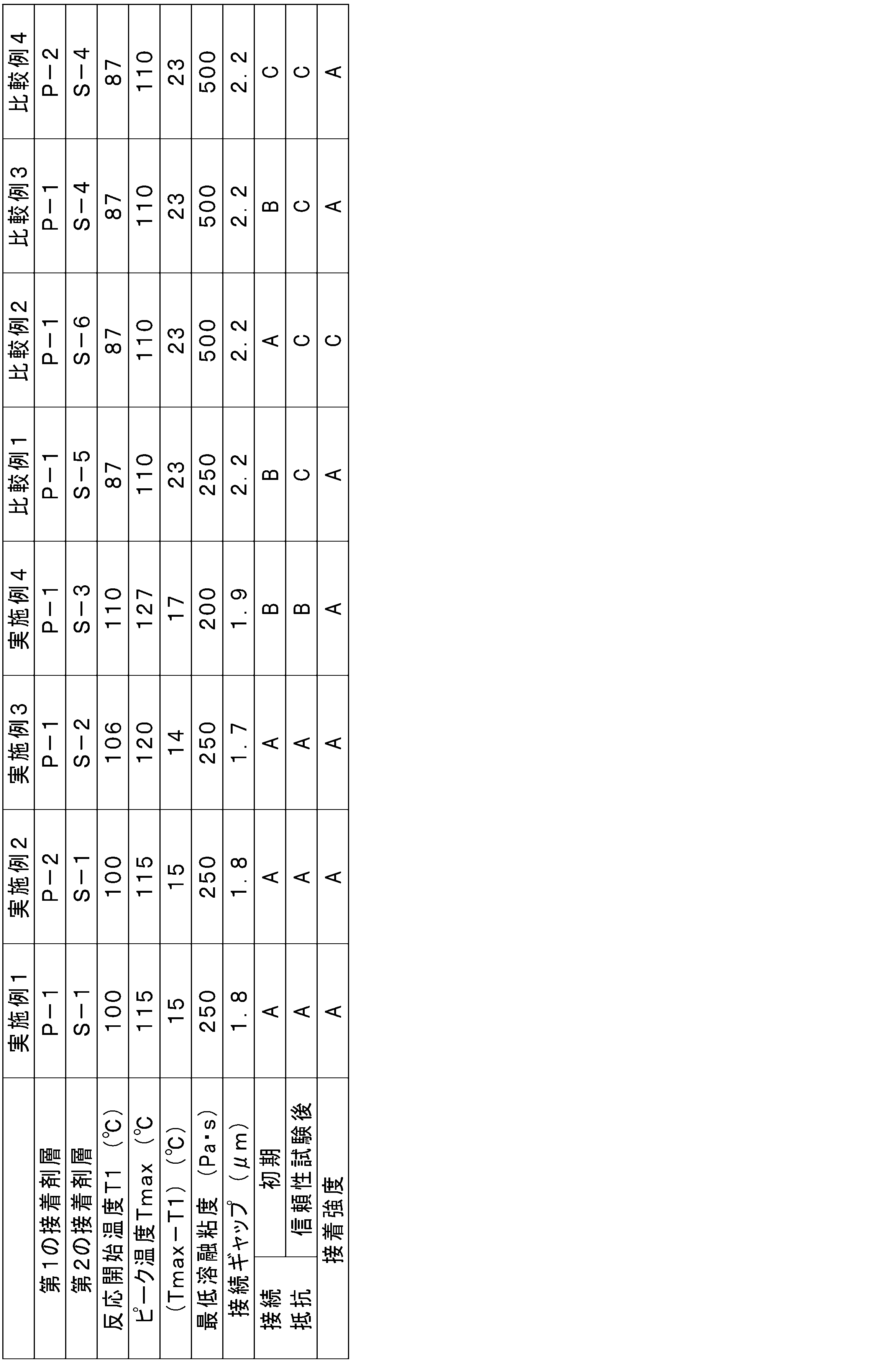
1…第1の接着剤層、2…第2の接着剤層、3…接着剤成分、4…導電粒子、10…回路接続用接着剤フィルム、21…第1の回路基板、22…第1の電極(回路電極)、23…第1の回路部材、24…第2の回路基板、25…第2の電極(バンプ電極)、26…第2の回路部材、27…回路接続部、100…回路接続構造体。 1...first adhesive layer, 2...second adhesive layer, 3...adhesive component, 4...conductive particles, 10...adhesive film for circuit connection, 21...first circuit board, 22...first electrode (circuit electrode), 23...first circuit member, 24...second circuit board, 25...second electrode (bump electrode), 26...second circuit member, 27...circuit connection portion, 100...circuit connection structure.
Claims (12)
前記回路接続用接着剤フィルムが、導電粒子及び第1の熱硬化性樹脂成分を含有する第1の接着剤層と、前記第1の接着剤層上に設けられた、第2の熱硬化性樹脂成分を含有する第2の接着剤層と、を有し、
前記回路接続用接着剤フィルムは、示差走査熱量曲線から得られる反応開始温度T1と反応ピーク温度Tmaxとの差(Tmax-T1)が20℃以下である、回路接続構造体の製造方法。 a step of interposing an adhesive film for circuit connection containing conductive particles between a first circuit member having a first electrode and a second circuit member having a second electrode, and thermocompressing the first circuit member and the second circuit member to electrically connect the first electrode and the second electrode to each other,
the adhesive film for circuit connection has a first adhesive layer containing conductive particles and a first thermosetting resin component, and a second adhesive layer provided on the first adhesive layer and containing a second thermosetting resin component,
A method for producing a circuit connection structure, wherein the adhesive film for circuit connection has a difference (Tmax-T1) between a reaction initiation temperature T1 and a reaction peak temperature Tmax obtained from a differential scanning calorimetry curve of 20° C. or less.
加熱開始時から1秒後に前記接続温度の80%以上の温度となるように前記第1の回路部材及び前記第2の回路部材を熱圧着する、請求項1に記載の回路接続構造体の製造方法。 a connection temperature when the first circuit member and the second circuit member are thermocompression-bonded is 170 to 220° C.;
2. The method for producing a circuit connection structure according to claim 1, wherein the first circuit member and the second circuit member are thermocompression bonded so that the temperature reaches 80% or more of the connection temperature 1 second after heating is started.
前記第1の接着剤層が光硬化性樹脂成分の硬化物を更に含有し、
前記光硬化性樹脂成分がラジカル重合性化合物及び光ラジカル重合開始剤を含む、請求項1に記載の回路接続構造体の製造方法。 the first thermosetting resin component and the second thermosetting resin component contain a cationic polymerizable compound and a thermal cationic polymerization initiator,
The first adhesive layer further contains a cured product of a photocurable resin component,
The method for producing a circuit connection structure according to claim 1 , wherein the photocurable resin component contains a radically polymerizable compound and a photoradical polymerization initiator.
示差走査熱量曲線から得られる反応開始温度T1と反応ピーク温度Tmaxとの差(Tmax-T1)が20℃以下である、回路接続用接着剤フィルム。 A first adhesive layer containing conductive particles and a first thermosetting resin component, and a second adhesive layer provided on the first adhesive layer and containing a second thermosetting resin component,
An adhesive film for circuit connection, in which the difference (Tmax-T1) between the reaction initiation temperature T1 and the reaction peak temperature Tmax obtained from a differential scanning calorimetry curve is 20°C or less.
前記第1の接着剤層が光硬化性樹脂成分の硬化物を更に含有し、
前記光硬化性樹脂成分がラジカル重合性化合物及び光ラジカル重合開始剤を含む、請求項7に記載の回路接続用接着剤フィルム。 the first thermosetting resin component and the second thermosetting resin component contain a cationic polymerizable compound and a thermal cationic polymerization initiator,
The first adhesive layer further contains a cured product of a photocurable resin component,
8. The adhesive film for circuit connection according to claim 7, wherein the photocurable resin component comprises a radical polymerizable compound and a photoradical polymerization initiator.
第2の電極を有する第2の回路部材と、
前記第1の回路部材及び前記第2の回路部材の間に配置され、前記第1の電極及び前記第2の電極を互いに電気的に接続する回路接続部と、
を備え、
前記回路接続部が、請求項7~11のいずれか一項に記載の回路接続用接着剤フィルムの硬化体を含む、
回路接続構造体。 a first circuit member having a first electrode;
a second circuit member having a second electrode;
a circuit connection portion disposed between the first circuit member and the second circuit member, the circuit connection portion electrically connecting the first electrode and the second electrode to each other;
Equipped with
The circuit connection portion comprises a cured product of the adhesive film for circuit connection according to any one of claims 7 to 11.
Circuit connection structure.
Priority Applications (4)
| Application Number | Priority Date | Filing Date | Title |
|---|---|---|---|
| JP2023191576A JP2025079110A (en) | 2023-11-09 | 2023-11-09 | Method for producing circuit connection structure, adhesive film for circuit connection, and circuit connection structure |
| CN202480069649.0A CN122123125A (en) | 2023-11-09 | 2024-10-02 | Method for manufacturing circuit connection structure, adhesive film for circuit connection, and circuit connection structure |
| PCT/JP2024/035287 WO2025100135A1 (en) | 2023-11-09 | 2024-10-02 | Manufacturing method for circuit connection structure, adhesive film for circuit connection, and circuit connection structure |
| KR1020267016753A KR20260109845A (en) | 2023-11-09 | 2024-10-02 | Method for manufacturing a circuit connection structure, adhesive film for circuit connection, and circuit connection structure |
Applications Claiming Priority (1)
| Application Number | Priority Date | Filing Date | Title |
|---|---|---|---|
| JP2023191576A JP2025079110A (en) | 2023-11-09 | 2023-11-09 | Method for producing circuit connection structure, adhesive film for circuit connection, and circuit connection structure |
Publications (1)
| Publication Number | Publication Date |
|---|---|
| JP2025079110A true JP2025079110A (en) | 2025-05-21 |
Family
ID=95695334
Family Applications (1)
| Application Number | Title | Priority Date | Filing Date |
|---|---|---|---|
| JP2023191576A Pending JP2025079110A (en) | 2023-11-09 | 2023-11-09 | Method for producing circuit connection structure, adhesive film for circuit connection, and circuit connection structure |
Country Status (4)
| Country | Link |
|---|---|
| JP (1) | JP2025079110A (en) |
| KR (1) | KR20260109845A (en) |
| CN (1) | CN122123125A (en) |
| WO (1) | WO2025100135A1 (en) |
Family Cites Families (3)
| Publication number | Priority date | Publication date | Assignee | Title |
|---|---|---|---|---|
| JP2010121007A (en) * | 2008-11-18 | 2010-06-03 | Sumitomo Electric Ind Ltd | Anisotropic electroconductive film |
| JP5768454B2 (en) * | 2011-04-14 | 2015-08-26 | デクセリアルズ株式会社 | Anisotropic conductive film |
| JPWO2023106410A1 (en) * | 2021-12-10 | 2023-06-15 |
-
2023
- 2023-11-09 JP JP2023191576A patent/JP2025079110A/en active Pending
-
2024
- 2024-10-02 WO PCT/JP2024/035287 patent/WO2025100135A1/en active Pending
- 2024-10-02 CN CN202480069649.0A patent/CN122123125A/en active Pending
- 2024-10-02 KR KR1020267016753A patent/KR20260109845A/en active Pending
Also Published As
| Publication number | Publication date |
|---|---|
| KR20260109845A (en) | 2026-07-13 |
| CN122123125A (en) | 2026-05-29 |
| WO2025100135A1 (en) | 2025-05-15 |
Similar Documents
| Publication | Publication Date | Title |
|---|---|---|
| JP7736001B2 (en) | Adhesive film for circuit connection, circuit connection structure and method for manufacturing the same | |
| JP7859314B2 (en) | Adhesive film for circuit connection, circuit connection structure, and method for manufacturing the same. | |
| WO2023106410A1 (en) | Adhesive film for circuit connection, and circuit connection structure and method for producing same | |
| CN116601250A (en) | Adhesive film for circuit connection, circuit connection structure and manufacturing method thereof | |
| WO2022102573A1 (en) | Circuit-connection adhesive film and method for producing same, and circuit connection structure and method for producing same | |
| JP7800429B2 (en) | Adhesive film for circuit connection, adhesive composition for circuit connection, circuit connection structure and method for producing the same | |
| WO2024034464A1 (en) | Adhesive film for circuit connection, circuit connection structure, and manufacturing method therefor | |
| WO2023106400A1 (en) | Adhesive film for circuit connection, and circuit connection structure and manufacturing method therefor | |
| WO2025100135A1 (en) | Manufacturing method for circuit connection structure, adhesive film for circuit connection, and circuit connection structure | |
| JP2025079120A (en) | Method for producing circuit connection structure, adhesive film for circuit connection, and circuit connection structure | |
| JP2023086476A (en) | Adhesive film for circuit connection, circuit connection structure and method for producing the same | |
| WO2022075370A1 (en) | Adhesive film for circuit connection, material for circuit connection, circuit connection structure, and method for manufacturing circuit connection structure | |
| JP7622448B2 (en) | Method for producing circuit connection adhesive and connection structure | |
| JP2022061623A (en) | Adhesive film for circuit connection as well as circuit connection structure and manufacturing method thereof | |
| JP2025034613A (en) | Adhesive film for circuit connection, circuit connection structure and method for producing same | |
| JP2025034640A (en) | Adhesive film for circuit connection, circuit connection structure and method for producing same | |
| CN116348563B (en) | Adhesive film for circuit connection, composition containing inorganic filler, circuit connection structure and method for producing the same |